KR20210007845A - Copper foil for flexible printed substrate - Google Patents
Copper foil for flexible printed substrate Download PDFInfo
- Publication number
- KR20210007845A KR20210007845A KR1020200076302A KR20200076302A KR20210007845A KR 20210007845 A KR20210007845 A KR 20210007845A KR 1020200076302 A KR1020200076302 A KR 1020200076302A KR 20200076302 A KR20200076302 A KR 20200076302A KR 20210007845 A KR20210007845 A KR 20210007845A
- Authority
- KR
- South Korea
- Prior art keywords
- copper foil
- copper
- orientation
- flexible printed
- less
- Prior art date
Links
Images

Classifications
-
- C—CHEMISTRY; METALLURGY
- C22—METALLURGY; FERROUS OR NON-FERROUS ALLOYS; TREATMENT OF ALLOYS OR NON-FERROUS METALS
- C22C—ALLOYS
- C22C9/00—Alloys based on copper
-
- B—PERFORMING OPERATIONS; TRANSPORTING
- B21—MECHANICAL METAL-WORKING WITHOUT ESSENTIALLY REMOVING MATERIAL; PUNCHING METAL
- B21B—ROLLING OF METAL
- B21B1/00—Metal-rolling methods or mills for making semi-finished products of solid or profiled cross-section; Sequence of operations in milling trains; Layout of rolling-mill plant, e.g. grouping of stands; Succession of passes or of sectional pass alternations
- B21B1/40—Metal-rolling methods or mills for making semi-finished products of solid or profiled cross-section; Sequence of operations in milling trains; Layout of rolling-mill plant, e.g. grouping of stands; Succession of passes or of sectional pass alternations for rolling foils which present special problems, e.g. because of thinness
-
- C—CHEMISTRY; METALLURGY
- C22—METALLURGY; FERROUS OR NON-FERROUS ALLOYS; TREATMENT OF ALLOYS OR NON-FERROUS METALS
- C22F—CHANGING THE PHYSICAL STRUCTURE OF NON-FERROUS METALS AND NON-FERROUS ALLOYS
- C22F1/00—Changing the physical structure of non-ferrous metals or alloys by heat treatment or by hot or cold working
- C22F1/08—Changing the physical structure of non-ferrous metals or alloys by heat treatment or by hot or cold working of copper or alloys based thereon
-
- H—ELECTRICITY
- H05—ELECTRIC TECHNIQUES NOT OTHERWISE PROVIDED FOR
- H05K—PRINTED CIRCUITS; CASINGS OR CONSTRUCTIONAL DETAILS OF ELECTRIC APPARATUS; MANUFACTURE OF ASSEMBLAGES OF ELECTRICAL COMPONENTS
- H05K1/00—Printed circuits
- H05K1/02—Details
- H05K1/09—Use of materials for the conductive, e.g. metallic pattern
Abstract
Description
본 발명은 플렉시블 프린트 기판 등의 배선 부재에 사용하기에 적합한 구리박에 관한 것이다.The present invention relates to a copper foil suitable for use in wiring members such as flexible printed circuit boards.
전자 기기의 소형, 박형, 고성능화에 수반하여, 플렉시블 프린트 기판(플렉시블 배선판, 이하, 「FPC」라고 칭함)이 널리 사용되고 있다.Along with the miniaturization, thinness, and high performance of electronic devices, flexible printed circuit boards (flexible wiring boards, hereinafter referred to as "FPC") are widely used.
FPC는 구리박과 수지를 적층한 Copper Clad Laminate(동장 적층체, 이하 CCL이라고 칭함)를 에칭함으로써 배선을 형성하고, 그 위를 커버 레이라고 불리는 수지층에 의해 피복한 것이다.In FPC, wiring is formed by etching a Copper Clad Laminate (copper clad laminate, hereinafter referred to as CCL) in which copper foil and resin are laminated, and the top is covered with a resin layer called a coverlay.
그런데, FPC의 도체인 구리박에는, 굴곡성과 함께, 절곡을 반복해도 파단하기 어려운 내절곡 특성이 요구되고, 또한 고속 전송 특성도 요구되고 있다.By the way, the copper foil, which is a conductor of the FPC, is required not only to have bendability, but also to have a bending resistance that is difficult to break even if bending is repeated, and a high speed transmission characteristic is also required.
통상, FPC용 구리박에는 표면에 조화 입자라고 칭해지는 미세한 금속 입자를 형성시키는 조화 처리가 실시되고, 또한 내열성이나 내약품성, 접착성을 부여하기 위하여 각종 표면 처리가 실시된다. 그리고, 이 구리박을, 필름상의 절연성 수지 기재와 가압 라미네이트하는 공법이나, 절연성 수지 기재를 구리박에 도포 후, 건조 또는 고온 처리하는 공법 등에 의해, CCL이 형성되고, 마지막으로 구리박 부분을 에칭하여 회로 형성하여 FPC가 제조된다.Usually, the FPC copper foil is subjected to a roughening treatment to form fine metal particles called roughened particles on the surface, and various surface treatments are performed to impart heat resistance, chemical resistance, and adhesiveness. Then, CCL is formed by a method of pressure-laminating this copper foil with a film-like insulating resin substrate, or a method of applying the insulating resin substrate to the copper foil and then drying or high temperature treatment, etc. to form CCL, and finally, the copper foil portion is etched. By forming a circuit, the FPC is manufactured.
그리고, 압연 구리박의 절곡성을 향상시키는 방법으로서, 최종 압하율을 높게 하여 재결정 집합 조직의 Cube(큐브) 방위인 입방체 집합 조직을 발달시키는 것이 알려져 있지만, 최종 압하율이 높으면, 변형이 축적되어서 연화 온도가 낮아진다는 문제가 있다.And, as a method of improving the bendability of the rolled copper foil, it is known to increase the final reduction ratio to develop a cubic texture, which is the cube orientation of the recrystallized texture, but when the final reduction ratio is high, deformation is accumulated. There is a problem that the softening temperature is lowered.
그래서, 최종 압하율을 높게 하지 않아도, 압연 구리박의 절곡성을 향상시키는 방책으로서, Copper(구리) 방위의 결정 방위 밀도를 10 이상으로 하고, Brass(황동) 방위의 결정 방위 밀도를 20 이상으로 하는 기술이 개발되어 있다(특허문헌 1).Therefore, as a measure to improve the bendability of the rolled copper foil without increasing the final reduction ratio, the crystal orientation density of the copper (copper) orientation is set to 10 or more, and the crystal orientation density of the brass (brass) orientation is set to 20 or more. A technique has been developed (Patent Document 1).
그런데, 단체의 구리박을 한번 절곡하면, 절곡 개소가 가공 경화하고, 다음번의 절곡 시에 가공 경화한 개소를 피하여 절곡된다. 이에 비해, 구리박을 지지체(수지)과 적층시킨 CCL을 절곡하면, 절곡 개소가 수지에 의해 구속되기 때문에, 동일 개소가 절곡되어, 구리박 단체보다도 엄격한 절곡 시험이 된다.By the way, when the single copper foil is bent once, the bending point is work-hardened, and it is bent while avoiding the work-hardened part at the time of the next bending. On the other hand, when the CCL obtained by laminating the copper foil with the support (resin) is bent, the bent position is constrained by the resin, so that the same position is bent, resulting in a more severe bending test than the copper foil alone.
그리고, 특허문헌 1에 기재된 기술과 같이, Copper 방위의 결정 방위 밀도를 높게 하면, 재결정 집합 조직에 있어서 Cube 방위가 발달하고, 재결정 입경이 커지기 때문에, CCL의 절곡성이 저하되는 것이 판명되었다.And, as in the technique described in Patent Document 1, when the crystal orientation density of the copper orientation is increased, the cube orientation develops in the recrystallized texture, and the recrystallization grain size increases, so that the bendability of CCL is deteriorated.
또한, Brass 방위의 결정 방위 밀도가 높으면, 재결정 집합 조직에 있어서 Brass 방위로 이루어지는 집합 조직이 발달한다. Brass 방위는 변형을 갖기 쉬운 방위이고, 절곡 시에 변형이 해방되어서 크랙이 발생하기 쉬워, CCL의 절곡성이 떨어진다.In addition, when the crystal orientation density of the brass orientation is high, an aggregate structure made of the brass orientation develops in the recrystallized texture. Brass orientation is an orientation that tends to have deformation, and the deformation is released at the time of bending and cracks are likely to occur, and the bendability of CCL is poor.
본 발명은 상기의 과제를 해결하기 위하여 이루어진 것이고, CCL의 절곡성을 향상시킨 플렉시블 프린트 기판용 구리박의 제공을 목적으로 한다.The present invention has been made in order to solve the above problems, and an object of the present invention is to provide a copper foil for a flexible printed circuit board having improved bendability of CCL.
본 발명자들은 여러가지 검토한 결과, CCL의 절곡성을 향상시키기 위해서는, 재결정 후의 Cube 방위의 발달을 억제하는, 즉 압연 조직의 단계에서 Copper 방위의 존재 비율을 억제할 필요가 있는 것을 발견하였다. 또한, CCL의 절곡성을 열화시키는 Brass 방위의 결정 방위 밀도도 저감하기로 하였다.As a result of various studies, the present inventors found that in order to improve the bendability of CCL, it is necessary to suppress the development of the cube orientation after recrystallization, that is, to suppress the proportion of the copper orientation at the stage of the rolling structure. In addition, it was decided to reduce the crystal orientation density of the brass orientation which deteriorates the bendability of CCL.
즉, 본 발명의 플렉시블 프린트 기판용 구리박은, 99.9질량% 이상의 Cu와, 첨가 원소로서 0.0005 내지 0.0220질량%의 P를 함유하고, 잔부 불가피적 불순물을 포함하는 압연 구리박이며, Copper 방위의 결정 방위 밀도가 10 미만이고, Brass 방위의 결정 방위 밀도가 20 미만이다.That is, the copper foil for flexible printed circuit boards of the present invention is a rolled copper foil containing 99.9% by mass or more of Cu and 0.0005 to 0.0220% by mass of P as an additive element, and remaining unavoidable impurities. The density is less than 10, and the crystal orientation density of the Brass orientation is less than 20.
Copper 방위와 Brass 방위는 각각, {112} <111>, {110} <112>로 정의된다.Copper orientation and Brass orientation are defined as {112} <111> and {110} <112>, respectively.
본 발명의 플렉시블 프린트 기판용 구리박은, JIS-H3100(C1100)에 규격하는 터프 피치 구리 또는 JIS-H3100(C1020)의 무산소 구리에, 첨가 원소로서 0.0005 내지 0.0220질량%의 P를 함유해도 된다.The copper foil for flexible printed circuit boards of the present invention may contain 0.0005 to 0.0220% by mass of P as an additive element in tough pitch copper according to JIS-H3100 (C1100) or oxygen-free copper according to JIS-H3100 (C1020).
본 발명의 플렉시블 프린트 기판용 구리박은, 표면 조도 Sa가 0.2㎛ 미만이면 된다.The copper foil for flexible printed circuit boards of the present invention may have a surface roughness Sa of less than 0.2 µm.
본 발명의 플렉시블 프린트 기판용 구리박은, 두께가 12㎛ 이하이면 된다.The copper foil for flexible printed circuit boards of the present invention may have a thickness of 12 µm or less.
본 발명에 따르면, CCL의 절곡성을 향상시킨 플렉시블 프린트 기판용 구리박이 얻어진다.According to the present invention, a copper foil for flexible printed circuit boards with improved bendability of CCL is obtained.
도 1은, 구리조를 최종 어닐링하기 위한 열처리 온도를 구하는 방법을 도시하는 도면이다.
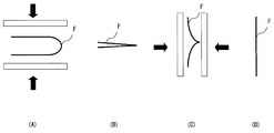
도 2는, 절곡 시험을 도시하는 도면이다.1 is a diagram showing a method of obtaining a heat treatment temperature for final annealing a copper bath.
2 is a diagram illustrating a bending test.
이하, 본 발명에 따른 구리박의 실시 형태에 대하여 설명한다. 또한, 본 발명에 있어서 %는 특별히 언급하지 않는 한, 질량%를 나타내는 것으로 한다.Hereinafter, an embodiment of the copper foil according to the present invention will be described. In addition, in the present invention,% is assumed to represent mass% unless otherwise specified.
<조성><Composition>
본 발명에 따른 구리박은, 99.9질량% 이상의 Cu와, 첨가 원소로서 0.0005 내지 0.0220질량%의 P를 함유하고, 잔부 불가피적 불순물을 포함한다. Cu가 99.96질량% 이상이면 바람직하다.The copper foil according to the present invention contains 99.9% by mass or more of Cu and 0.0005 to 0.0220% by mass of P as an additive element, and the remainder contains inevitable impurities. It is preferable that Cu is 99.96 mass% or more.
첨가 원소로서 P를 함유하면, Copper 방위의 결정 방위 밀도를 10 미만으로 할 수 있다.When P is contained as an additional element, the crystal orientation density of the copper orientation can be made less than 10.
P의 함유량이 0.0005질량%(5질량ppm) 미만이면, Copper 방위의 결정 방위 밀도가 10 이상으로 되고, CCL의 절곡성이 저하된다. P의 함유량이 0.0220질량%(220질량ppm)를 초과하면, 도전율이 저하되어, 플렉시블 프린트 기판에 적합하지 않다.When the P content is less than 0.0005 mass% (5 mass ppm), the crystal orientation density of the copper orientation becomes 10 or more, and the bendability of CCL is deteriorated. When the P content exceeds 0.0220 mass% (220 mass ppm), the electrical conductivity is lowered, which is not suitable for a flexible printed circuit board.
본 발명에 따른 구리박을, JIS-H3100(C1100)에 규격하는 터프 피치 구리 또는 JIS-H3100(C1020)의 무산소 구리에, 첨가 원소로서 0.0005 내지 0.0220질량%의 P를 함유하여 이루어지는 조성으로 해도 된다.The copper foil according to the present invention may be a composition comprising 0.0005 to 0.0220% by mass of P as an additional element in tough pitch copper according to JIS-H3100 (C1100) or oxygen-free copper according to JIS-H3100 (C1020). .
<결정 방위 밀도><Crystal orientation density>
구리박의 Copper 방위의 결정 방위 밀도가 10 미만이다. 상술한 바와 같이, CCL의 절곡성을 향상시키기 위해서는, 재결정 후의 Cube 방위의 발달을 억제하는, 즉 압연 조직의 단계에서 Copper 방위의 존재 비율을 억제할 필요가 있다.The crystal orientation density of the copper orientation of the copper foil is less than 10. As described above, in order to improve the bendability of CCL, it is necessary to suppress the development of the cube orientation after recrystallization, that is, to suppress the presence ratio of the copper orientation at the stage of the rolling structure.
Copper 방위의 결정 방위 밀도가 10 이상이 되면, 재결정 후에 Cube 방위가 발달하고, 재결정 입경이 커져서 CCL의 절곡성이 저하된다.If the crystal orientation density of the copper orientation is more than 10, the cube orientation develops after recrystallization, and the recrystallization grain size increases, resulting in a decrease in the bendability of CCL.
구리박의 Brass 방위의 결정 방위 밀도가 20 미만이다. Brass 방위는 변형을 갖기 쉽고, Brass 방위의 결정 방위 밀도가 20 이상이면, 절곡 시에 변형이 해방되어서 크랙이 발생하기 쉬워, CCL의 절곡성이 저하된다.The crystal orientation density of the brass orientation of copper foil is less than 20. The brass orientation is easy to have deformation, and if the crystal orientation density of the brass orientation is 20 or more, the deformation is released at the time of bending and cracks are liable to occur, and the bendability of CCL is deteriorated.
결정 방위 밀도는, 완전 극점도를 사용하여 산출하였다. 완전 극점도는, 불완전 극점도를 사용하여 산출하였다. 불완전 극점도는, 압연 집합 조직의 X선 극도형 측정에 의해 얻을 수 있다. X선 극도형 측정에는 리가쿠제 RINT2500(상품명)을 사용하고, 구리박의 (111), (200), (220)의 면에 대해서, Schultz의 반사법의 조건으로 X선 극도형 측정을 행하였다. 측정 조건은, 입사 X선원: Co, 관전압: 30kV, 관전류: 100mA, 발산 슬릿: 1°, 산란 슬릿: 0.05mm, 수광 슬릿: 0.05mm, 발산 세로 제한 슬릿: 1.2mm, 주사 속도: 360°/min, 스텝 폭: 5°의 조건에서 행한다. 각 면에 있어서 회절 강도를 측정한 2θ의 범위(θ는 회절 각도)는, (111): 48.0 내지 54.0°, (200): 56.5 내지 62.5°, (220): 86.0 내지 92.0°이다.The crystal orientation density was calculated using the complete pole figure. The complete pole figure was calculated using the incomplete pole figure. The incomplete pole figure can be obtained by X-ray extreme-type measurement of the rolled texture. RINT2500 (brand name) manufactured by Rigaku was used for the X-ray extreme measurement, and X-ray extreme measurement was performed on the (111), (200), and (220) surfaces of the copper foil under the conditions of Schultz's reflection method. Measurement conditions are incident X-ray source: Co, tube voltage: 30kV, tube current: 100mA, divergence slit: 1°, scattering slit: 0.05mm, light receiving slit: 0.05mm, divergence vertical limiting slit: 1.2mm, scanning speed: 360°/ min, step width: 5°. The range of 2θ in which the diffraction intensity was measured on each side (θ is the diffraction angle) is (111): 48.0 to 54.0°, (200): 56.5 to 62.5°, and (220): 86.0 to 92.0°.
X선 극도형 측정으로 얻어진 불완전 극점도의 데이터 처리에는, 리가쿠제 RINT2500 부속 정극 점 데이터 처리 소프트웨어를 사용하였다. 처리 조건은, RD 보정, 스무싱, 백그라운드 처리, random 규격화이다. 처리한 데이터는 리가쿠제 ASC 변환 소프트웨어를 사용하여 텍스트 변환하였다.For data processing of the incomplete pole figure obtained by X-ray extreme type measurement, the positive pole data processing software attached to RINT2500 manufactured by Rigaku was used. The processing conditions are RD correction, smoothing, background processing, and random standardization. The processed data was converted into text using Rigaku's ASC conversion software.
텍스트 데이터화한 불완전 극점도로부터 완전 극점도로의 변환과 결정 방위 분포 함수의 추출에는 Standard ODF Ver2.4를 사용하였다. 또한, Copper 방위 및 Brass 방위는 오일러각 공간 상에 복수 개소 나타나기 때문에, 본 발명에서는 결정 방위 밀도 함수 f(gCopper) 및 f(gBrass)의 오일러각은, gCopper=(90°, 35°, 45°) 및 gBrass=(35°, 45°, 90°)를 채용하였다.Standard ODF Ver2.4 was used for the conversion from text data-generated incomplete pole map to perfect pole figure and extraction of the crystal orientation distribution function. In addition, since the copper orientation and the brass orientation appear in plural places on the Euler angle space, in the present invention, the Euler angles of the crystal orientation density functions f (gCopper) and f (gBrass) are gCopper = (90 °, 35 °, 45 ° ) And gBrass=(35°, 45°, 90°) were employed.
구리박의 표면 조도 Sa가 0.2㎛ 미만인 것이 바람직하다. 표면 조도 Sa가 0.2㎛ 미만이면, 구리박을 FPC로 했을 때의 전송 손실을 억제할 수 있다.It is preferable that the surface roughness Sa of the copper foil is less than 0.2 µm. When the surface roughness Sa is less than 0.2 µm, transmission loss when the copper foil is used as FPC can be suppressed.
표면 조도 Sa는 ISO25178로 규정된다.The surface roughness S a is specified by ISO25178.
구리박의 두께는, JISC6515에 규정되는 공칭 두께로 12㎛ 이하가 바람직하다. 두께가 얇을수록, 구리박에 가하는 응력이 작아지기 때문에 절곡성의 향상에 이바지함과 함께 포터블 기기의 소형화, 박형화, 경량화에도 이바지한다.The thickness of the copper foil is preferably 12 µm or less in terms of the nominal thickness specified in JIS C6515. The thinner the thickness, the smaller the stress applied to the copper foil, thus contributing to the improvement of bendability and contributing to miniaturization, reduction in thickness, and weight reduction of portable devices.
본 발명의 구리박은, 예를 들어 이하와 같이 하여 제조할 수 있다. 먼저, 구리 잉곳에 P를 첨가하여 용해, 주조한 후, 열간 압연하고, 냉간 압연과 어닐링을 반복하여 행함으로써 박을 제조할 수 있다. 또한, 어닐링은 1회여도 된다.The copper foil of this invention can be manufactured as follows, for example. First, P is added to a copper ingot, melted and cast, and then hot-rolled, cold-rolling and annealing are repeatedly performed, whereby a foil can be manufactured. In addition, annealing may be performed once.
여기서, 어닐링 중 마지막으로 행하는 것을 최종 어닐링이라고 칭하고, 최종 어닐링 전후의 냉간 압연을 각각 최종 어닐링 전 냉간 압연, 최종 어닐링 후 냉간 압연이라고 칭한다.Here, what is performed last during annealing is called final annealing, and cold rolling before and after final annealing is called cold rolling before final annealing and cold rolling after final annealing, respectively.
여기서, 최종 어닐링 전 냉간 압연의 압하율은, 80% 이상으로 하는 것이 바람직하다. 구리조에 충분한 변형을 축적시키기 위해서이다.Here, it is preferable that the rolling reduction ratio of cold rolling before final annealing is 80% or more. This is to accumulate sufficient strain in the copper bath.
최종 어닐링 후 냉간 압연의 압하율(최종 압하율)은 95% 이상이 바람직하고, 더욱 바람직하게는 99% 이상이다. 압하율이 95% 이하이면, 구리박에 축적되는 변형이 불균일하기 때문에, 압연 조직이 불균일해진다. 또한, 압하율이 95% 이상이면 Copper 방위의 성장이 억제되기 때문이다.The rolling reduction ratio (final reduction ratio) of cold rolling after the final annealing is preferably 95% or more, more preferably 99% or more. If the reduction ratio is 95% or less, since the strain accumulated in the copper foil is uneven, the rolling structure becomes uneven. Moreover, this is because the growth of the copper orientation is suppressed when the reduction ratio is 95% or more.
압하율(R)은, 압연 전의 박 두께를 T0, 압연 후의 박 두께 T1로 하고, 압하율 R={(T0-T1)/T0}×100으로 표시된다.The reduction ratio R is represented by the reduction ratio R={(T 0 -T 1 )/T 0 }×100, with the foil thickness before rolling as T 0 and the thickness T 1 after rolling.
최종 어닐링의 열처리 조건을 제어함으로써, Copper 방위 및 Brass 방위를 억제할 수 있다.By controlling the heat treatment conditions of the final annealing, copper orientation and brass orientation can be suppressed.
여기서, 최종 어닐링의 열처리 온도로서는, 「재결정」 영역의 온도로 한다. 최종 어닐링의 열처리 온도를 「회복」 상태의 온도로 하면, 최종 어닐링 후 냉간 압연에 의해 Brass 방위가 발달해 버린다. 「회복」 상태보다도 고온이 되도록, 최종 어닐링의 열처리 온도를 「입성장」 상태의 온도로 하면, 최종 어닐링 후 냉간 압연에 의해 Copper 방위가 발달해 버린다. 이 때문에, 최종 어닐링의 열처리 온도를 「재결정」 영역이 되도록 설정한다.Here, as the heat treatment temperature of the final annealing, the temperature in the "recrystallization" region is used. If the heat treatment temperature of the final annealing is set to a temperature in the "recovery" state, the brass orientation will develop by cold rolling after the final annealing. When the heat treatment temperature of the final annealing is set to the temperature of the "grain growth" state so that it becomes higher than the "recovery" state, the copper orientation will develop by cold rolling after the final annealing. For this reason, the heat treatment temperature of final annealing is set so that it may become a "recrystallization" region.
「재결정」 영역 온도는, 이하의 방법에 의해 결정할 수 있다.The "recrystallization" region temperature can be determined by the following method.
먼저, 최종 어닐링 전 냉간 압연 후에 최종 어닐링 전의 구리조를, 25, 100, 150℃, 200 내지 260℃까지 10℃ 간격, 280, 300, 350, 380, 400℃까지 온도를 변화시키고, 30분간, 질소 분위기 하에서 열처리를 행했을 때의 항장력(N/㎟)을 JISZ2241에 준거하여 각각 측정한다.First, after cold rolling before the final annealing, the copper bath before the final annealing was changed to 25, 100, 150°C, 200 to 260°C at 10°C intervals, 280, 300, 350, 380, 400°C, and 30 minutes, The tensile strength (N/mm 2) when heat treatment is performed in a nitrogen atmosphere is measured in accordance with JISZ2241, respectively.
이어서, 도 1에 도시한 바와 같이, 열처리 온도를 X축, 항장력을 Y축으로 한 그래프에 측정 데이터를 플롯한다. 저온측(25℃)으로부터 고온측을 향하여, 인접하는 플롯 간에서 항장력이 10MPa/10℃ 이상으로 급격하게 저하되는 점을 변곡점 1이라 한다. 변곡점 1로부터 고온측을 향하여, 인접하는 플롯 간에서 항장력이 10MPa/10℃ 미만이 된 점을 변곡점 2라 한다. 변곡점 2로부터 고온측을 향하여, 인접하는 플롯 간에서 항장력이 5% 이상으로 저하된 점을 변곡점 3이라 한다.Next, as shown in Fig. 1, the measurement data is plotted on a graph in which the heat treatment temperature is the X axis and the tensile strength is the Y axis. From the low temperature side (25°C) toward the high temperature side, the point in which the tensile strength rapidly decreases to 10 MPa/10°C or more between adjacent plots is referred to as inflection point 1. The point where the tensile strength between adjacent plots from the inflection point 1 toward the high temperature side becomes less than 10 MPa/10°C is referred to as the inflection point 2. The point at which the tensile strength decreased to 5% or more between adjacent plots from the inflection point 2 toward the high temperature side is referred to as the inflection point 3.
변곡점 2보다 저온을 「회복 영역」, 변곡점 2 이상 또한 변곡점 3 미만의 온도를 「재결정 영역」, 변곡점 3 이상의 고온을 「입성장 영역」이라 한다.A lower temperature than the inflection point 2 is referred to as a "recovery region", a temperature equal to or higher than the inflection point 2 and lower than the inflection point 3 is referred to as a "recrystallization region", and a high temperature higher than the inflection point 3 is referred to as a "grain growth region".
이와 같이, 최종 어닐링의 열처리 온도를 「재결정 영역」이 되도록 설정하고, 최종 어닐링을 질소 분위기 하에서, 유지 시간이 1분 내지 30분으로 행하는 것이 바람직하다.In this way, it is preferable that the heat treatment temperature of the final annealing is set to be a "recrystallized region", and the final annealing is performed in a nitrogen atmosphere and the holding time is 1 to 30 minutes.
또한, 본 발명은, 상기 실시 형태에 한정되지 않는다. 또한, 본 발명의 작용 효과를 발휘하는 한, 상기 실시 형태에 있어서의 구리 합금이 그 밖의 성분을 함유해도 된다.In addition, this invention is not limited to the said embodiment. In addition, the copper alloy in the above embodiment may contain other components as long as the effects of the present invention are exhibited.
예를 들어, 구리박의 표면에, 조화 처리, 방청 처리, 내열 처리 또는 이들의 조합에 의한 표면 처리를 실시해도 된다.For example, you may perform surface treatment by roughening treatment, rust prevention treatment, heat resistance treatment, or a combination thereof on the surface of the copper foil.
[실시예][Example]
이어서, 실시예를 들어 본 발명을 더욱 상세하게 설명하지만, 본 발명은 이들에 한정되는 것은 아니다.Next, the present invention will be described in more detail with reference to examples, but the present invention is not limited thereto.
무산소 구리(JIS-H3100C1020)에 대하여, 표 1에 기재된 원소를 첨가한 잉곳을 제작하였다. 이 잉곳을 900℃ 전후에서 열간 압연, 냉간 압연이 가해진 후에, 어닐링을 가하여 표면의 산화 스케일 제거를 위한 면삭을 행하였다. 그 후에, 다단식의 냉간 압연기에 의해 압연 구리조의 두께가 2.0mm가 될 때까지 최종 어닐링 전 냉간 압연하였다. 그 후, 상기한 방법으로 결정한 최종 어닐링의 열처리 온도(도 1의 재결정 영역의 최저 온도인 변곡점 2의 온도)에서, 질소 분위기 하에서 30분간의 최종 어닐링을 행하였다. 그 후, 최종 구리박 두께인 12㎛까지 압하율 99.4%로 최종 어닐링 후 냉간 압연을 행하였다.For oxygen-free copper (JIS-H3100C1020), an ingot to which the elements shown in Table 1 were added was produced. The ingot was subjected to hot rolling and cold rolling at around 900°C, followed by annealing to perform chamfering to remove oxide scale from the surface. After that, cold-rolling was performed before the final annealing until the thickness of the rolled copper bath became 2.0 mm by a multistage cold rolling mill. Thereafter, the final annealing was performed for 30 minutes in a nitrogen atmosphere at the heat treatment temperature of the final annealing determined by the above method (the temperature of the inflection point 2, which is the lowest temperature in the recrystallization region in Fig. 1). Then, cold rolling was performed after final annealing at a reduction ratio of 99.4% to the final copper foil thickness of 12 µm.
<구리박 샘플의 평가><Evaluation of copper foil sample>
1. 도전율1. Conductivity
상기 최종 냉간 압연 후의 각 구리박 샘플에 대해서, JIS H 0505에 기초하여 4단자법에 의해, 20℃의 도전율(%IACS)을 측정하였다.For each copper foil sample after the final cold rolling, the electrical conductivity (%IACS) at 20°C was measured by a four-terminal method based on JIS H 0505.
도전율이 80% IACS보다 크면 도전성이 양호하다.If the conductivity is greater than 80% IACS, the conductivity is good.
2. 구리박의 표면 조도 Sa2. Surface roughness Sa of copper foil
상기 최종 냉간 압연 후의 각 구리박 샘플에 대해서, 표면 조도 Sa를 ISO25178을 따라서 측정하였다.For each copper foil sample after the final cold rolling, the surface roughness S a was measured according to ISO25178.
각 실시예 및 비교예의 구리박의 표면 조도 Sa는 0.1이었다.The surface roughness Sa of the copper foil of each Example and the comparative example was 0.1.
3. 결정 방위 밀도(Copper 방위 및 Brass 방위)3. Crystal orientation density (Copper orientation and Brass orientation)
상술한 바와 같이 하여 측정하였다.It was measured as described above.
4. 내절곡 특성4. Bending resistance
상기 최종 냉간 압연 후의 각 구리박 샘플로부터 플렉시블 프린트 배선판을 제작하고, 절곡 시험하여 내절곡 특성을 평가하였다.A flexible printed wiring board was prepared from each copper foil sample after the final cold rolling, and a bending test was performed to evaluate the bending resistance.
플렉시블 프린트 배선판은 하기와 같이 제작하였다. 폴리이미드 수지 필름(가부시키가이샤 가네카제 FRS-142#SW; 두께 25um)의 양면에 각각 구리박 샘플을 적층하고, 진공 열 프레스로 360℃에서 5분간 가열하여 동장 적층판을 제작하였다. 이 동장 적층판의 편측의 구리박을 전체면 에칭으로 제거하고, 다른 측의 구리박에는, MD(압연 평행 방향)에 평행해지도록 L(라인)/S(스페이스)=300㎛/300㎛의 회로를 8개 형성하여 플렉시블 프린트 배선판으로 하였다.The flexible printed wiring board was produced as follows. Copper foil samples were laminated on both sides of a polyimide resin film (FRS-142#SW manufactured by Kaneka, Inc.; thickness 25um), respectively, and heated at 360°C for 5 minutes by a vacuum hot press to prepare a copper clad laminate. The copper foil on one side of the copper clad laminate was removed by etching the entire surface, and the copper foil on the other side was subjected to a circuit of L (line)/S (space) = 300 µm/300 µm so as to be parallel to MD (rolling parallel direction). Eight were formed to obtain a flexible printed wiring board.
도 2에 도시하는 바와 같이 하여 절곡 시험을 행하였다. 먼저, (A)에 도시하는 바와 같이, 플렉시블 프린트 배선판 F를 절곡하여 지그에 의해 구리측이 외측이 되도록 하고, (B)와 같이 절곡하였다. 계속해서, 절곡한 플렉시블 프린트 배선판 F를 되돌려 지그를 사용하여 개방하고(C), 개방한 굽힘부를 평탄하게 되돌렸다(D). (A) 내지 (D)를 1회의 180° 밀착 굽힘으로 하고, 이것을 반복하였다.As shown in Fig. 2, a bending test was performed. First, as shown in (A), the flexible printed wiring board F was bent so that the copper side was outside by a jig, and it was bent as in (B). Subsequently, the bent flexible printed wiring board F was returned and opened using a jig (C), and the opened bent portion was returned flat (D). (A) to (D) were made one 180° close bending, and this was repeated.
절곡 횟수는 이하와 같이 판정하였다. 즉, 1회의 180° 밀착 굽힘마다, 플렉시블 프린트 배선판의 구리박 회로에 일정 전류를 흘리고, 당해 전류를 흘리기 위하여 필요한 전압값을 측정하고, 측정한 전압값으로부터 플렉시블 프린트 배선판의 구리박 회로의 저항값을 산출하였다. 산출한 저항값이 초기값(상기 절곡 전의 저항값)의 120% 이상으로 되었을 때에, 파단이 발생했다고 판정하였다.The number of bending was determined as follows. That is, for each 180° close bending, a constant current is passed through the copper foil circuit of the flexible printed wiring board, the voltage value required to pass the current is measured, and the resistance value of the copper foil circuit of the flexible printed wiring board from the measured voltage value Was calculated. When the calculated resistance value became 120% or more of the initial value (the resistance value before bending), it was determined that fracture occurred.
절곡 횟수는, 파단한 직전까지의 180° 밀착 굽힘의 횟수로 하였다.The number of bendings was taken as the number of 180° close-contact bending until just before fracture.
또한, 절곡 시험은, 각 구리박 샘플에 대해서, 플렉시블 프린트 배선판을 5매 제작해서 n=5로 행하고, 각 시험에서의 절곡 횟수의 평균값을 채용하였다. 절곡 횟수가 5회 이상이면 양호하다.In addition, in the bending test, for each copper foil sample, five flexible printed wiring boards were produced, n = 5, and the average value of the number of times of bending in each test was adopted. It is good if the number of bending is 5 or more.
얻어진 결과를 표 1에 나타내었다.Table 1 shows the obtained results.

표 1로부터 명백해진 바와 같이, Copper 방위의 결정 방위 밀도가 10 미만, 또한 Brass 방위의 결정 방위 밀도가 20 미만인 각 실시예의 경우, 내절곡 특성이 우수하고, 구리박 단체보다 가혹한 CCL의 절곡성이 향상되었다.As apparent from Table 1, in the case of each example in which the crystal orientation density of the copper orientation is less than 10, and the crystal orientation density of the brass orientation is less than 20, the bending resistance is excellent, and the bending property of CCL, which is harsher than the copper foil alone, is Improved.
한편, 최종 어닐링 온도를 「회복」 상태의 온도로 한 비교예 1, 2의 경우, 최종 냉간 압연에 의해 Brass 방위가 발달하고, Brass 방위의 결정 방위 밀도가 20 이상으로 되고, 내절곡 특성이 떨어졌다. 또한, 비교예 1의 경우, P가 첨가되어 있지 않으므로 Copper 방위가 성장하기 쉬워지고, 그의 결정 방위 밀도가 10 이상이 되었다.On the other hand, in the case of Comparative Examples 1 and 2 in which the final annealing temperature was the temperature in the ``recovery'' state, the brass orientation was developed by the final cold rolling, the crystal orientation density of the brass orientation became 20 or more, and the bending resistance was poor. lost. Moreover, in the case of Comparative Example 1, since P was not added, the copper orientation became easy to grow, and the crystal orientation density thereof became 10 or more.
P의 함유량이 0.0005질량%(5질량ppm) 미만인 비교예 3의 경우, Copper 방위의 결정 방위 밀도가 10 이상으로 되고, 내절곡 특성이 떨어졌다.In the case of Comparative Example 3 in which the P content was less than 0.0005 mass% (5 mass ppm), the crystal orientation density of the copper orientation was 10 or more, and the bending resistance was inferior.
최종 어닐링 온도를 「회복」 상태보다도 고온인 「입성장」 상태의 온도로 한 비교예 4, 5의 경우, 최종 냉간 압연에 의해 Copper 방위가 발달하고, 그의 결정 방위 밀도가 10 이상으로 되고, 내절곡 특성이 떨어졌다.In the case of Comparative Examples 4 and 5 in which the final annealing temperature was a temperature in the "grain growth" state higher than the "recovery" state, the copper orientation was developed by the final cold rolling, and the crystal orientation density thereof became 10 or more. The bending properties were poor.
Claims (4)
Copper 방위의 결정 방위 밀도가 10 미만이고, Brass 방위의 결정 방위 밀도가 20 미만인 플렉시블 프린트 기판용 구리박.It is a rolled copper foil containing 99.9 mass% or more of Cu, and 0.0005 to 0.0220 mass% of P as an additive element, and remaining unavoidable impurities,
Copper foil for flexible printed circuit boards with a crystal orientation density of less than 10 in a copper orientation and less than 20 in a brass orientation.
Priority Applications (1)
| Application Number | Priority Date | Filing Date | Title |
|---|---|---|---|
| KR1020220048908A KR20220054767A (en) | 2019-07-10 | 2022-04-20 | Copper foil for flexible printed substrate |
Applications Claiming Priority (2)
| Application Number | Priority Date | Filing Date | Title |
|---|---|---|---|
| JPJP-P-2019-128145 | 2019-07-10 | ||
| JP2019128145A JP7186141B2 (en) | 2019-07-10 | 2019-07-10 | Copper foil for flexible printed circuit boards |
Related Child Applications (1)
| Application Number | Title | Priority Date | Filing Date |
|---|---|---|---|
| KR1020220048908A Division KR20220054767A (en) | 2019-07-10 | 2022-04-20 | Copper foil for flexible printed substrate |
Publications (1)
| Publication Number | Publication Date |
|---|---|
| KR20210007845A true KR20210007845A (en) | 2021-01-20 |
Family
ID=74058821
Family Applications (2)
| Application Number | Title | Priority Date | Filing Date |
|---|---|---|---|
| KR1020200076302A KR20210007845A (en) | 2019-07-10 | 2020-06-23 | Copper foil for flexible printed substrate |
| KR1020220048908A KR20220054767A (en) | 2019-07-10 | 2022-04-20 | Copper foil for flexible printed substrate |
Family Applications After (1)
| Application Number | Title | Priority Date | Filing Date |
|---|---|---|---|
| KR1020220048908A KR20220054767A (en) | 2019-07-10 | 2022-04-20 | Copper foil for flexible printed substrate |
Country Status (4)
| Country | Link |
|---|---|
| JP (2) | JP7186141B2 (en) |
| KR (2) | KR20210007845A (en) |
| CN (1) | CN112210689B (en) |
| TW (1) | TWI747330B (en) |
Families Citing this family (1)
| Publication number | Priority date | Publication date | Assignee | Title |
|---|---|---|---|---|
| US20240072108A1 (en) | 2021-02-01 | 2024-02-29 | Rohm Co., Ltd. | Sic semiconductor device |
Citations (1)
| Publication number | Priority date | Publication date | Assignee | Title |
|---|---|---|---|---|
| JPH0142020Y2 (en) | 1984-06-18 | 1989-12-11 |
Family Cites Families (14)
| Publication number | Priority date | Publication date | Assignee | Title |
|---|---|---|---|---|
| GB2091634B (en) * | 1981-01-22 | 1984-12-05 | Gen Electric | Transfer lamination of vapour deposited copper thin sheets and films |
| JPH01319641A (en) * | 1988-06-21 | 1989-12-25 | Hitachi Cable Ltd | Soft rolled copper foil and flexible printed board |
| JP4118832B2 (en) * | 2004-04-14 | 2008-07-16 | 三菱伸銅株式会社 | Copper alloy and manufacturing method thereof |
| JP4992940B2 (en) * | 2009-06-22 | 2012-08-08 | 日立電線株式会社 | Rolled copper foil |
| JP5752536B2 (en) * | 2011-08-23 | 2015-07-22 | Jx日鉱日石金属株式会社 | Rolled copper foil |
| CN107046763B (en) * | 2016-02-05 | 2019-12-24 | Jx金属株式会社 | Copper foil for flexible printed board and copper-clad laminate using same |
| CN107046768B (en) * | 2016-02-05 | 2019-12-31 | Jx金属株式会社 | Copper foil for flexible printed board, copper-clad laminate using same, flexible printed board, and electronic device |
| JP6328679B2 (en) * | 2016-03-28 | 2018-05-23 | Jx金属株式会社 | Copper foil for flexible printed circuit board, copper-clad laminate using the same, flexible printed circuit board, and electronic device |
| JP2016211077A (en) * | 2016-07-26 | 2016-12-15 | Jx金属株式会社 | Titanium copper |
| JP6617313B2 (en) * | 2017-08-03 | 2019-12-11 | Jx金属株式会社 | Copper foil for flexible printed circuit board, copper-clad laminate using the same, flexible printed circuit board, and electronic device |
| JP6647253B2 (en) * | 2017-08-03 | 2020-02-14 | Jx金属株式会社 | Copper foil for flexible printed circuit board, copper-clad laminate using the same, flexible printed circuit board, and electronic device |
| JP6643287B2 (en) * | 2017-08-03 | 2020-02-12 | Jx金属株式会社 | Copper foil for flexible printed circuit board, copper-clad laminate using the same, flexible printed circuit board, and electronic device |
| JP6442020B1 (en) * | 2017-10-12 | 2018-12-19 | 福田金属箔粉工業株式会社 | Hard rolled copper foil and method for producing the hard rolled copper foil |
| CN108246804B (en) * | 2018-01-12 | 2019-11-05 | 中色奥博特铜铝业有限公司 | A kind of preparation method of high bending performance rolled copper foil |
-
2019
- 2019-07-10 JP JP2019128145A patent/JP7186141B2/en active Active
-
2020
- 2020-06-16 TW TW109120157A patent/TWI747330B/en active
- 2020-06-23 KR KR1020200076302A patent/KR20210007845A/en not_active Application Discontinuation
- 2020-07-10 CN CN202010662207.0A patent/CN112210689B/en active Active
-
2022
- 2022-04-11 JP JP2022064896A patent/JP2022095855A/en not_active Ceased
- 2022-04-20 KR KR1020220048908A patent/KR20220054767A/en active Application Filing
Patent Citations (1)
| Publication number | Priority date | Publication date | Assignee | Title |
|---|---|---|---|---|
| JPH0142020Y2 (en) | 1984-06-18 | 1989-12-11 |
Also Published As
| Publication number | Publication date |
|---|---|
| CN112210689A (en) | 2021-01-12 |
| JP2021014603A (en) | 2021-02-12 |
| TW202106885A (en) | 2021-02-16 |
| JP7186141B2 (en) | 2022-12-08 |
| JP2022095855A (en) | 2022-06-28 |
| KR20220054767A (en) | 2022-05-03 |
| TWI747330B (en) | 2021-11-21 |
| CN112210689B (en) | 2021-12-14 |
Similar Documents
| Publication | Publication Date | Title |
|---|---|---|
| JP4716520B2 (en) | Rolled copper foil | |
| JP4672515B2 (en) | Rolled copper alloy foil for bending | |
| KR101935128B1 (en) | Copper foil for flexible printed wiring board, copper-clad laminate using the same, flexible printed wiring board and electronic device | |
| KR102098479B1 (en) | Copper foil for flexible printed circuit, copper clad laminate using the same, flexible printed circuit and electronic device | |
| JP6294257B2 (en) | Copper alloy foil for flexible printed circuit board, copper-clad laminate using the same, flexible printed circuit board, and electronic device | |
| JP3824593B2 (en) | Rolled copper foil with high elongation | |
| KR102470725B1 (en) | Copper foil for flexible printed circuit, and copper clad laminate, flexible printed circuit and electronic device using copper foil | |
| JP6781562B2 (en) | Copper foil for flexible printed circuit boards, copper-clad laminates using it, flexible printed circuit boards, and electronic devices | |
| KR20210007845A (en) | Copper foil for flexible printed substrate | |
| KR20170113104A (en) | Copper foil for flexible printed wiring board, copper-clad laminate using the same, flexible printed wiring board and electronic device | |
| JP2015175005A (en) | Rolled copper foil, copper-clad laminate sheet and flexible printed wiring board and electronic equipment | |
| CN107046763B (en) | Copper foil for flexible printed board and copper-clad laminate using same | |
| JP5753115B2 (en) | Rolled copper foil for printed wiring boards | |
| KR102227339B1 (en) | Hard-rolled copper foil and manufacturing method of the hard-rolled copper foil | |
| KR20190133736A (en) | Rolled copper foil | |
| KR102136096B1 (en) | Copper foil for flexible printed substrate, and copper clad laminate using the same, flexible printed substrate and electronic equipment | |
| JP6647253B2 (en) | Copper foil for flexible printed circuit board, copper-clad laminate using the same, flexible printed circuit board, and electronic device | |
| KR101721314B1 (en) | Rolled copper foil, copper clad laminate, and flexible printed board and electronic device | |
| JP4427044B2 (en) | Conductor for flexible substrate, method for producing the same, and flexible substrate | |
| CN111757599A (en) | Copper foil for flexible printed board, copper-clad laminate using same, flexible printed board, and electronic device | |
| JP2019214793A (en) | Rolled copper foil, copper-clad laminate, flexible printed wiring board, electronic equipment, and method for manufacturing rolled copper foil | |
| JP6030325B2 (en) | Rolled copper foil, copper-clad laminate, flexible printed wiring board, and electronic equipment | |
| KR20200038410A (en) | Copper foil for flexible printed substrate, copper-clad laminate using the same, flexible printed substrate, and electronic equipment | |
| Kuwako et al. | A new very low profile electrodeposited copper foil | |
| JP2009302562A (en) | Conductor for flexible board, its production process and flexible board |
Legal Events
| Date | Code | Title | Description |
|---|---|---|---|
| E902 | Notification of reason for refusal | ||
| E601 | Decision to refuse application | ||
| J201 | Request for trial against refusal decision | ||
| J301 | Trial decision |
Free format text: TRIAL NUMBER: 2022101000908; TRIAL DECISION FOR APPEAL AGAINST DECISION TO DECLINE REFUSAL REQUESTED 20220420 Effective date: 20221122 |