KR20210002345A - 마이크로리소그래피용 마스크를 측정하기 위한 장치 및 오토포커싱 방법 - Google Patents
마이크로리소그래피용 마스크를 측정하기 위한 장치 및 오토포커싱 방법 Download PDFInfo
- Publication number
- KR20210002345A KR20210002345A KR1020200078351A KR20200078351A KR20210002345A KR 20210002345 A KR20210002345 A KR 20210002345A KR 1020200078351 A KR1020200078351 A KR 1020200078351A KR 20200078351 A KR20200078351 A KR 20200078351A KR 20210002345 A KR20210002345 A KR 20210002345A
- Authority
- KR
- South Korea
- Prior art keywords
- mask
- imaging
- focal
- focusing
- plane
- Prior art date
- Legal status (The legal status is an assumption and is not a legal conclusion. Google has not performed a legal analysis and makes no representation as to the accuracy of the status listed.)
- Ceased
Links
Images

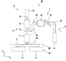


Classifications
-
- G—PHYSICS
- G03—PHOTOGRAPHY; CINEMATOGRAPHY; ANALOGOUS TECHNIQUES USING WAVES OTHER THAN OPTICAL WAVES; ELECTROGRAPHY; HOLOGRAPHY
- G03F—PHOTOMECHANICAL PRODUCTION OF TEXTURED OR PATTERNED SURFACES, e.g. FOR PRINTING, FOR PROCESSING OF SEMICONDUCTOR DEVICES; MATERIALS THEREFOR; ORIGINALS THEREFOR; APPARATUS SPECIALLY ADAPTED THEREFOR
- G03F9/00—Registration or positioning of originals, masks, frames, photographic sheets or textured or patterned surfaces, e.g. automatically
- G03F9/70—Registration or positioning of originals, masks, frames, photographic sheets or textured or patterned surfaces, e.g. automatically for microlithography
- G03F9/7003—Alignment type or strategy, e.g. leveling, global alignment
- G03F9/7023—Aligning or positioning in direction perpendicular to substrate surface
- G03F9/7026—Focusing
-
- G—PHYSICS
- G03—PHOTOGRAPHY; CINEMATOGRAPHY; ANALOGOUS TECHNIQUES USING WAVES OTHER THAN OPTICAL WAVES; ELECTROGRAPHY; HOLOGRAPHY
- G03F—PHOTOMECHANICAL PRODUCTION OF TEXTURED OR PATTERNED SURFACES, e.g. FOR PRINTING, FOR PROCESSING OF SEMICONDUCTOR DEVICES; MATERIALS THEREFOR; ORIGINALS THEREFOR; APPARATUS SPECIALLY ADAPTED THEREFOR
- G03F1/00—Originals for photomechanical production of textured or patterned surfaces, e.g., masks, photo-masks, reticles; Mask blanks or pellicles therefor; Containers specially adapted therefor; Preparation thereof
- G03F1/68—Preparation processes not covered by groups G03F1/20 - G03F1/50
- G03F1/82—Auxiliary processes, e.g. cleaning or inspecting
- G03F1/84—Inspecting
-
- H—ELECTRICITY
- H04—ELECTRIC COMMUNICATION TECHNIQUE
- H04N—PICTORIAL COMMUNICATION, e.g. TELEVISION
- H04N23/00—Cameras or camera modules comprising electronic image sensors; Control thereof
- H04N23/60—Control of cameras or camera modules
- H04N23/67—Focus control based on electronic image sensor signals
-
- G—PHYSICS
- G02—OPTICS
- G02B—OPTICAL ELEMENTS, SYSTEMS OR APPARATUS
- G02B21/00—Microscopes
- G02B21/0004—Microscopes specially adapted for specific applications
- G02B21/002—Scanning microscopes
- G02B21/0024—Confocal scanning microscopes (CSOMs) or confocal "macroscopes"; Accessories which are not restricted to use with CSOMs, e.g. sample holders
- G02B21/0052—Optical details of the image generation
- G02B21/006—Optical details of the image generation focusing arrangements; selection of the plane to be imaged
-
- G—PHYSICS
- G02—OPTICS
- G02B—OPTICAL ELEMENTS, SYSTEMS OR APPARATUS
- G02B21/00—Microscopes
- G02B21/24—Base structure
- G02B21/241—Devices for focusing
- G02B21/244—Devices for focusing using image analysis techniques
-
- G—PHYSICS
- G02—OPTICS
- G02B—OPTICAL ELEMENTS, SYSTEMS OR APPARATUS
- G02B21/00—Microscopes
- G02B21/24—Base structure
- G02B21/241—Devices for focusing
- G02B21/245—Devices for focusing using auxiliary sources, detectors
-
- G—PHYSICS
- G02—OPTICS
- G02B—OPTICAL ELEMENTS, SYSTEMS OR APPARATUS
- G02B7/00—Mountings, adjusting means, or light-tight connections, for optical elements
- G02B7/28—Systems for automatic generation of focusing signals
-
- G—PHYSICS
- G02—OPTICS
- G02B—OPTICAL ELEMENTS, SYSTEMS OR APPARATUS
- G02B7/00—Mountings, adjusting means, or light-tight connections, for optical elements
- G02B7/28—Systems for automatic generation of focusing signals
- G02B7/36—Systems for automatic generation of focusing signals using image sharpness techniques, e.g. image processing techniques for generating autofocus signals
- G02B7/38—Systems for automatic generation of focusing signals using image sharpness techniques, e.g. image processing techniques for generating autofocus signals measured at different points on the optical axis, e.g. focussing on two or more planes and comparing image data
-
- G—PHYSICS
- G06—COMPUTING OR CALCULATING; COUNTING
- G06T—IMAGE DATA PROCESSING OR GENERATION, IN GENERAL
- G06T7/00—Image analysis
- G06T7/0002—Inspection of images, e.g. flaw detection
- G06T7/0004—Industrial image inspection
-
- G—PHYSICS
- G06—COMPUTING OR CALCULATING; COUNTING
- G06T—IMAGE DATA PROCESSING OR GENERATION, IN GENERAL
- G06T7/00—Image analysis
- G06T7/60—Analysis of geometric attributes
-
- G—PHYSICS
- G06—COMPUTING OR CALCULATING; COUNTING
- G06T—IMAGE DATA PROCESSING OR GENERATION, IN GENERAL
- G06T2207/00—Indexing scheme for image analysis or image enhancement
- G06T2207/10—Image acquisition modality
- G06T2207/10141—Special mode during image acquisition
- G06T2207/10148—Varying focus
-
- G—PHYSICS
- G06—COMPUTING OR CALCULATING; COUNTING
- G06T—IMAGE DATA PROCESSING OR GENERATION, IN GENERAL
- G06T2207/00—Indexing scheme for image analysis or image enhancement
- G06T2207/30—Subject of image; Context of image processing
- G06T2207/30108—Industrial image inspection
- G06T2207/30148—Semiconductor; IC; Wafer
Landscapes
- Physics & Mathematics (AREA)
- General Physics & Mathematics (AREA)
- Engineering & Computer Science (AREA)
- Optics & Photonics (AREA)
- Computer Vision & Pattern Recognition (AREA)
- Chemical & Material Sciences (AREA)
- Analytical Chemistry (AREA)
- Theoretical Computer Science (AREA)
- Quality & Reliability (AREA)
- Geometry (AREA)
- Signal Processing (AREA)
- Multimedia (AREA)
- Automatic Focus Adjustment (AREA)
- Exposure And Positioning Against Photoresist Photosensitive Materials (AREA)
- Microscoopes, Condenser (AREA)
- Length Measuring Devices By Optical Means (AREA)
- Focusing (AREA)
- Preparing Plates And Mask In Photomechanical Process (AREA)
- Exposure Of Semiconductors, Excluding Electron Or Ion Beam Exposure (AREA)
- Studio Devices (AREA)
Applications Claiming Priority (2)
| Application Number | Priority Date | Filing Date | Title |
|---|---|---|---|
| DE102019117293.4 | 2019-06-27 | ||
| DE102019117293.4A DE102019117293B3 (de) | 2019-06-27 | 2019-06-27 | Vorrichtung zur Vermessung von Masken für die Mikrolithographie und Autofokussierverfahren |
Publications (1)
| Publication Number | Publication Date |
|---|---|
| KR20210002345A true KR20210002345A (ko) | 2021-01-07 |
Family
ID=72839203
Family Applications (1)
| Application Number | Title | Priority Date | Filing Date |
|---|---|---|---|
| KR1020200078351A Ceased KR20210002345A (ko) | 2019-06-27 | 2020-06-26 | 마이크로리소그래피용 마스크를 측정하기 위한 장치 및 오토포커싱 방법 |
Country Status (6)
| Country | Link |
|---|---|
| US (1) | US11647288B2 (https=) |
| JP (1) | JP7382904B2 (https=) |
| KR (1) | KR20210002345A (https=) |
| CN (1) | CN112147858B (https=) |
| DE (1) | DE102019117293B3 (https=) |
| TW (1) | TWI794612B (https=) |
Cited By (1)
| Publication number | Priority date | Publication date | Assignee | Title |
|---|---|---|---|---|
| KR20230062412A (ko) * | 2021-10-29 | 2023-05-09 | 칼 짜이스 에스엠티 게엠베하 | 반도체 리소그라피용 기판 측정 방법 |
Families Citing this family (1)
| Publication number | Priority date | Publication date | Assignee | Title |
|---|---|---|---|---|
| DE102023119683B4 (de) * | 2023-07-25 | 2025-12-18 | Carl Zeiss Smt Gmbh | Verfahren zur Bestimmung einer Lage einer Objektoberfläche |
Family Cites Families (18)
| Publication number | Priority date | Publication date | Assignee | Title |
|---|---|---|---|---|
| US6677565B1 (en) * | 1998-08-18 | 2004-01-13 | Veeco Tucson Inc. | High speed autofocus and tilt for an optical imaging system |
| US6124924A (en) * | 1998-12-24 | 2000-09-26 | Applied Materials, Inc. | Focus error correction method and apparatus |
| JP3688185B2 (ja) * | 2000-05-08 | 2005-08-24 | 株式会社東京精密 | 焦点検出装置及び自動焦点顕微鏡 |
| DE10153113A1 (de) * | 2001-08-15 | 2003-03-13 | Aglaia Ges Fuer Bildverarbeitu | Verfahren und Vorrichtung zur Entfernungsbestimmung |
| US6688565B1 (en) | 2002-10-01 | 2004-02-10 | Kupo Co., Ltd. | Multi-leg stand |
| US7142315B1 (en) * | 2004-01-16 | 2006-11-28 | Kla-Tencor Technologies Corporation | Slit confocal autofocus system |
| JP2009031169A (ja) * | 2007-07-28 | 2009-02-12 | Nikon Corp | 位置検出装置、露光装置、及びデバイスの製造方法 |
| US9229209B2 (en) * | 2008-01-21 | 2016-01-05 | Carl Zeiss Smt Gmbh | Autofocus device and autofocusing method for an imaging device |
| JPWO2009093594A1 (ja) * | 2008-01-24 | 2011-05-26 | 株式会社ニコン | 面位置検出装置、露光装置、およびデバイス製造方法 |
| JP5498044B2 (ja) | 2009-03-26 | 2014-05-21 | 株式会社東芝 | 自動焦点調節機構及び光学画像取得装置 |
| JP5757099B2 (ja) * | 2010-02-15 | 2015-07-29 | 株式会社ニコン | 焦点調節装置、及び焦点調節プログラム |
| JP5293782B2 (ja) | 2011-07-27 | 2013-09-18 | 三星ダイヤモンド工業株式会社 | 合焦位置調整方法、合焦位置調整装置、およびレーザー加工装置 |
| DE102011082414A1 (de) | 2011-09-09 | 2013-03-14 | Carl Zeiss Sms Gmbh | Autofokuseinrichtung und Autofokussierverfahren für eine Abbildungsvorrichtung |
| DE102012223128B4 (de) * | 2012-12-13 | 2022-09-01 | Carl Zeiss Microscopy Gmbh | Autofokusverfahren für Mikroskop und Mikroskop mit Autofokuseinrichtung |
| DE102014114864B4 (de) * | 2014-10-14 | 2016-06-02 | Carl Zeiss Sms Gmbh | Verfahren und Vorrichtung zum Ermitteln eines lateralen Versatzes eines Musters auf einem Substrat relativ zu einer Sollposition |
| CN106772923B (zh) | 2015-11-24 | 2021-01-01 | 睿励科学仪器(上海)有限公司 | 基于倾斜狭缝的自动对焦方法和系统 |
| DE102016120730A1 (de) | 2016-10-31 | 2018-02-08 | Carl Zeiss Smt Gmbh | Autofokussiereinrichtung für eine Abbildungsvorrichtung sowie Autofokussierverfahren |
| JP7079569B2 (ja) * | 2017-04-21 | 2022-06-02 | 株式会社ニューフレアテクノロジー | 検査方法 |
-
2019
- 2019-06-27 DE DE102019117293.4A patent/DE102019117293B3/de active Active
-
2020
- 2020-06-24 CN CN202010593805.7A patent/CN112147858B/zh active Active
- 2020-06-24 TW TW109121561A patent/TWI794612B/zh active
- 2020-06-26 KR KR1020200078351A patent/KR20210002345A/ko not_active Ceased
- 2020-06-26 US US16/912,837 patent/US11647288B2/en active Active
- 2020-06-26 JP JP2020110384A patent/JP7382904B2/ja active Active
Cited By (1)
| Publication number | Priority date | Publication date | Assignee | Title |
|---|---|---|---|---|
| KR20230062412A (ko) * | 2021-10-29 | 2023-05-09 | 칼 짜이스 에스엠티 게엠베하 | 반도체 리소그라피용 기판 측정 방법 |
Also Published As
| Publication number | Publication date |
|---|---|
| JP7382904B2 (ja) | 2023-11-17 |
| JP2021006903A (ja) | 2021-01-21 |
| CN112147858B (zh) | 2023-11-10 |
| US11647288B2 (en) | 2023-05-09 |
| US20200412939A1 (en) | 2020-12-31 |
| TW202107227A (zh) | 2021-02-16 |
| DE102019117293B3 (de) | 2020-11-05 |
| CN112147858A (zh) | 2020-12-29 |
| TWI794612B (zh) | 2023-03-01 |
Similar Documents
| Publication | Publication Date | Title |
|---|---|---|
| KR101625695B1 (ko) | 측정 장치를 구비한 마이크로리소그래피용 투영 노광 시스템 | |
| JP2924344B2 (ja) | 投影露光装置 | |
| US9268240B2 (en) | Exposure apparatus, exposure method, and device fabrication method | |
| KR102288614B1 (ko) | 특히 마이크로리소그라피용 광학 시스템에서 요소의 노광 동안 노광 에너지를 결정하기 위한 디바이스 | |
| US11947185B2 (en) | Autofocusing method for an imaging device | |
| KR20210002345A (ko) | 마이크로리소그래피용 마스크를 측정하기 위한 장치 및 오토포커싱 방법 | |
| JP5434352B2 (ja) | 表面検査装置および表面検査方法 | |
| US11898970B2 (en) | EUV mask inspection device using multilayer reflection zone plate | |
| JP2021006903A5 (https=) | ||
| US8988752B2 (en) | Beam control apparatus for an illumination beam and metrology system comprising an optical system containing such a beam control apparatus | |
| JP3518826B2 (ja) | 面位置検出方法及び装置並びに露光装置 | |
| JP2001077004A (ja) | 露光装置および電子線露光装置 | |
| KR20000011676A (ko) | 노출된시료의표면상에부분적인불균일이있는경우에도고도로정밀한노출을할수있는대전입자빔노출장치및노출방법 | |
| CN111443577B (zh) | 用于曝光设备的调整装置、方法及曝光设备 | |
| JPH10189428A (ja) | 照明光学装置 | |
| JP3003694B2 (ja) | 投影露光装置 | |
| JP6522529B2 (ja) | マスク検査方法およびマスク検査装置 | |
| JP2011064829A (ja) | パターン描画装置および描画方法 | |
| WO2026093151A1 (en) | Device for capturing images of structures on photolithographic masks | |
| WO2026093150A1 (en) | Device for capturing images of structures on photolithographic masks | |
| JP3202707B2 (ja) | 縮小投影露光装置を用いた計測方法及びその縮小投影露光装置 | |
| JP3673625B2 (ja) | 微細パターンの形成方法 | |
| KR101368601B1 (ko) | 결상 오차 결정부를 갖춘 광학 결상 장치 | |
| JPS6390825A (ja) | 自動焦点合わせ装置 | |
| JPH08162400A (ja) | 露光装置 |
Legal Events
| Date | Code | Title | Description |
|---|---|---|---|
| PA0109 | Patent application |
Patent event code: PA01091R01D Comment text: Patent Application Patent event date: 20200626 |
|
| PA0201 | Request for examination | ||
| AMND | Amendment | ||
| PG1501 | Laying open of application | ||
| E902 | Notification of reason for refusal | ||
| PE0902 | Notice of grounds for rejection |
Comment text: Notification of reason for refusal Patent event date: 20211028 Patent event code: PE09021S01D |
|
| AMND | Amendment | ||
| E601 | Decision to refuse application | ||
| PE0601 | Decision on rejection of patent |
Patent event date: 20220726 Comment text: Decision to Refuse Application Patent event code: PE06012S01D Patent event date: 20211028 Comment text: Notification of reason for refusal Patent event code: PE06011S01I |
|
| X091 | Application refused [patent] | ||
| PX0901 | Re-examination |
Patent event code: PX09011S01I Patent event date: 20220726 Comment text: Decision to Refuse Application Patent event code: PX09012R01I Patent event date: 20220228 Comment text: Amendment to Specification, etc. Patent event code: PX09012R01I Patent event date: 20200713 Comment text: Amendment to Specification, etc. |
|
| E601 | Decision to refuse application | ||
| E801 | Decision on dismissal of amendment | ||
| PE0601 | Decision on rejection of patent |
Patent event date: 20221118 Comment text: Decision to Refuse Application Patent event code: PE06012S01D Patent event date: 20211028 Comment text: Notification of reason for refusal Patent event code: PE06011S01I |
|
| PE0801 | Dismissal of amendment |
Patent event code: PE08012E01D Comment text: Decision on Dismissal of Amendment Patent event date: 20221118 Patent event code: PE08011R01I Comment text: Amendment to Specification, etc. Patent event date: 20221020 Patent event code: PE08011R01I Comment text: Amendment to Specification, etc. Patent event date: 20220228 Patent event code: PE08011R01I Comment text: Amendment to Specification, etc. Patent event date: 20200713 |