KR20200088449A - 플래너 폴리머 스택을 제조하는 방법 - Google Patents
플래너 폴리머 스택을 제조하는 방법 Download PDFInfo
- Publication number
- KR20200088449A KR20200088449A KR1020207018083A KR20207018083A KR20200088449A KR 20200088449 A KR20200088449 A KR 20200088449A KR 1020207018083 A KR1020207018083 A KR 1020207018083A KR 20207018083 A KR20207018083 A KR 20207018083A KR 20200088449 A KR20200088449 A KR 20200088449A
- Authority
- KR
- South Korea
- Prior art keywords
- layer
- block copolymer
- polymer
- top coat
- prepolymer
- Prior art date
- Legal status (The legal status is an assumption and is not a legal conclusion. Google has not performed a legal analysis and makes no representation as to the accuracy of the status listed.)
- Ceased
Links
- 229920000642 polymer Polymers 0.000 title claims abstract description 172
- 239000000203 mixture Substances 0.000 claims abstract description 153
- 238000004132 cross linking Methods 0.000 claims abstract description 120
- 238000000034 method Methods 0.000 claims abstract description 114
- 239000000178 monomer Substances 0.000 claims abstract description 83
- 239000007788 liquid Substances 0.000 claims abstract description 61
- 238000006243 chemical reaction Methods 0.000 claims abstract description 58
- 229920001577 copolymer Polymers 0.000 claims abstract description 53
- 239000000539 dimer Substances 0.000 claims abstract description 38
- 238000010438 heat treatment Methods 0.000 claims abstract description 28
- 238000004519 manufacturing process Methods 0.000 claims abstract description 15
- 229920001400 block copolymer Polymers 0.000 claims description 367
- 239000000758 substrate Substances 0.000 claims description 83
- 239000002904 solvent Substances 0.000 claims description 73
- 239000000463 material Substances 0.000 claims description 64
- 239000000126 substance Substances 0.000 claims description 57
- 230000009477 glass transition Effects 0.000 claims description 38
- -1 hydroxyalkyl acrylate Chemical compound 0.000 claims description 36
- 230000007935 neutral effect Effects 0.000 claims description 36
- LFQSCWFLJHTTHZ-UHFFFAOYSA-N Ethanol Chemical compound CCO LFQSCWFLJHTTHZ-UHFFFAOYSA-N 0.000 claims description 34
- 239000003054 catalyst Substances 0.000 claims description 34
- 239000007787 solid Substances 0.000 claims description 30
- 239000000470 constituent Substances 0.000 claims description 28
- 238000000151 deposition Methods 0.000 claims description 28
- 238000005329 nanolithography Methods 0.000 claims description 27
- 125000000524 functional group Chemical group 0.000 claims description 25
- 229920001651 Cyanoacrylate Polymers 0.000 claims description 24
- 239000002253 acid Substances 0.000 claims description 24
- IAZDPXIOMUYVGZ-UHFFFAOYSA-N Dimethylsulphoxide Chemical compound CS(C)=O IAZDPXIOMUYVGZ-UHFFFAOYSA-N 0.000 claims description 20
- 150000001412 amines Chemical class 0.000 claims description 20
- 238000000137 annealing Methods 0.000 claims description 20
- 239000003153 chemical reaction reagent Substances 0.000 claims description 19
- 150000001875 compounds Chemical class 0.000 claims description 19
- 230000008021 deposition Effects 0.000 claims description 19
- OKKJLVBELUTLKV-UHFFFAOYSA-N Methanol Chemical compound OC OKKJLVBELUTLKV-UHFFFAOYSA-N 0.000 claims description 18
- XUIMIQQOPSSXEZ-UHFFFAOYSA-N Silicon Chemical compound [Si] XUIMIQQOPSSXEZ-UHFFFAOYSA-N 0.000 claims description 18
- NAQMVNRVTILPCV-UHFFFAOYSA-N hexane-1,6-diamine Chemical compound NCCCCCCN NAQMVNRVTILPCV-UHFFFAOYSA-N 0.000 claims description 18
- 229910052710 silicon Inorganic materials 0.000 claims description 18
- 239000010703 silicon Substances 0.000 claims description 18
- 239000004593 Epoxy Substances 0.000 claims description 17
- CERQOIWHTDAKMF-UHFFFAOYSA-M Methacrylate Chemical compound CC(=C)C([O-])=O CERQOIWHTDAKMF-UHFFFAOYSA-M 0.000 claims description 16
- WEVYAHXRMPXWCK-UHFFFAOYSA-N Acetonitrile Chemical compound CC#N WEVYAHXRMPXWCK-UHFFFAOYSA-N 0.000 claims description 15
- LYCAIKOWRPUZTN-UHFFFAOYSA-N Ethylene glycol Chemical compound OCCO LYCAIKOWRPUZTN-UHFFFAOYSA-N 0.000 claims description 15
- ZMXDDKWLCZADIW-UHFFFAOYSA-N N,N-Dimethylformamide Chemical compound CN(C)C=O ZMXDDKWLCZADIW-UHFFFAOYSA-N 0.000 claims description 15
- DNIAPMSPPWPWGF-UHFFFAOYSA-N Propylene glycol Chemical compound CC(O)CO DNIAPMSPPWPWGF-UHFFFAOYSA-N 0.000 claims description 15
- ARXJGSRGQADJSQ-UHFFFAOYSA-N 1-methoxypropan-2-ol Chemical compound COCC(C)O ARXJGSRGQADJSQ-UHFFFAOYSA-N 0.000 claims description 14
- 150000003573 thiols Chemical class 0.000 claims description 14
- MWCLLHOVUTZFKS-UHFFFAOYSA-N Methyl cyanoacrylate Chemical compound COC(=O)C(=C)C#N MWCLLHOVUTZFKS-UHFFFAOYSA-N 0.000 claims description 13
- 239000002585 base Substances 0.000 claims description 13
- KFZMGEQAYNKOFK-UHFFFAOYSA-N Isopropanol Chemical compound CC(C)O KFZMGEQAYNKOFK-UHFFFAOYSA-N 0.000 claims description 12
- BMWDUGHMODRTLU-UHFFFAOYSA-N azanium;trifluoromethanesulfonate Chemical compound [NH4+].[O-]S(=O)(=O)C(F)(F)F BMWDUGHMODRTLU-UHFFFAOYSA-N 0.000 claims description 12
- LZCLXQDLBQLTDK-UHFFFAOYSA-N ethyl 2-hydroxypropanoate Chemical compound CCOC(=O)C(C)O LZCLXQDLBQLTDK-UHFFFAOYSA-N 0.000 claims description 12
- FPYJFEHAWHCUMM-UHFFFAOYSA-N maleic anhydride Chemical compound O=C1OC(=O)C=C1 FPYJFEHAWHCUMM-UHFFFAOYSA-N 0.000 claims description 12
- 238000006116 polymerization reaction Methods 0.000 claims description 12
- 125000000391 vinyl group Chemical group [H]C([*])=C([H])[H] 0.000 claims description 12
- 229920002554 vinyl polymer Polymers 0.000 claims description 12
- 238000007259 addition reaction Methods 0.000 claims description 11
- 239000000654 additive Substances 0.000 claims description 11
- 239000013626 chemical specie Substances 0.000 claims description 11
- 238000000407 epitaxy Methods 0.000 claims description 11
- 150000002989 phenols Chemical class 0.000 claims description 11
- 230000008569 process Effects 0.000 claims description 11
- YEJRWHAVMIAJKC-UHFFFAOYSA-N 4-Butyrolactone Chemical compound O=C1CCCO1 YEJRWHAVMIAJKC-UHFFFAOYSA-N 0.000 claims description 10
- MQJKPEGWNLWLTK-UHFFFAOYSA-N Dapsone Chemical compound C1=CC(N)=CC=C1S(=O)(=O)C1=CC=C(N)C=C1 MQJKPEGWNLWLTK-UHFFFAOYSA-N 0.000 claims description 10
- RPNUMPOLZDHAAY-UHFFFAOYSA-N Diethylenetriamine Chemical compound NCCNCCN RPNUMPOLZDHAAY-UHFFFAOYSA-N 0.000 claims description 10
- QIGBRXMKCJKVMJ-UHFFFAOYSA-N Hydroquinone Chemical compound OC1=CC=C(O)C=C1 QIGBRXMKCJKVMJ-UHFFFAOYSA-N 0.000 claims description 10
- DGAQECJNVWCQMB-PUAWFVPOSA-M Ilexoside XXIX Chemical compound C[C@@H]1CC[C@@]2(CC[C@@]3(C(=CC[C@H]4[C@]3(CC[C@@H]5[C@@]4(CC[C@@H](C5(C)C)OS(=O)(=O)[O-])C)C)[C@@H]2[C@]1(C)O)C)C(=O)O[C@H]6[C@@H]([C@H]([C@@H]([C@H](O6)CO)O)O)O.[Na+] DGAQECJNVWCQMB-PUAWFVPOSA-M 0.000 claims description 10
- YRKCREAYFQTBPV-UHFFFAOYSA-N acetylacetone Chemical compound CC(=O)CC(C)=O YRKCREAYFQTBPV-UHFFFAOYSA-N 0.000 claims description 10
- QGBSISYHAICWAH-UHFFFAOYSA-N dicyandiamide Chemical compound NC(N)=NC#N QGBSISYHAICWAH-UHFFFAOYSA-N 0.000 claims description 10
- GHMLBKRAJCXXBS-UHFFFAOYSA-N resorcinol Chemical compound OC1=CC=CC(O)=C1 GHMLBKRAJCXXBS-UHFFFAOYSA-N 0.000 claims description 10
- 229910052708 sodium Inorganic materials 0.000 claims description 10
- 239000011734 sodium Substances 0.000 claims description 10
- NIXOWILDQLNWCW-UHFFFAOYSA-M Acrylate Chemical compound [O-]C(=O)C=C NIXOWILDQLNWCW-UHFFFAOYSA-M 0.000 claims description 9
- WSMYVTOQOOLQHP-UHFFFAOYSA-N Malondialdehyde Chemical compound O=CCC=O WSMYVTOQOOLQHP-UHFFFAOYSA-N 0.000 claims description 9
- 150000003863 ammonium salts Chemical class 0.000 claims description 9
- 229920000768 polyamine Polymers 0.000 claims description 9
- CIWBSHSKHKDKBQ-JLAZNSOCSA-N Ascorbic acid Chemical compound OC[C@H](O)[C@H]1OC(=O)C(O)=C1O CIWBSHSKHKDKBQ-JLAZNSOCSA-N 0.000 claims description 8
- OKTJSMMVPCPJKN-UHFFFAOYSA-N Carbon Chemical compound [C] OKTJSMMVPCPJKN-UHFFFAOYSA-N 0.000 claims description 8
- FYYHWMGAXLPEAU-UHFFFAOYSA-N Magnesium Chemical compound [Mg] FYYHWMGAXLPEAU-UHFFFAOYSA-N 0.000 claims description 8
- 238000006482 condensation reaction Methods 0.000 claims description 8
- 229910052749 magnesium Inorganic materials 0.000 claims description 8
- 239000011777 magnesium Substances 0.000 claims description 8
- 229920006295 polythiol Polymers 0.000 claims description 8
- XLYOFNOQVPJJNP-UHFFFAOYSA-N water Substances O XLYOFNOQVPJJNP-UHFFFAOYSA-N 0.000 claims description 8
- YCNIBOIOWCTRCL-UHFFFAOYSA-N azane;2,2,2-trifluoroacetic acid Chemical compound [NH4+].[O-]C(=O)C(F)(F)F YCNIBOIOWCTRCL-UHFFFAOYSA-N 0.000 claims description 7
- 125000002091 cationic group Chemical group 0.000 claims description 7
- 238000005530 etching Methods 0.000 claims description 7
- 150000004693 imidazolium salts Chemical class 0.000 claims description 7
- 230000002269 spontaneous effect Effects 0.000 claims description 7
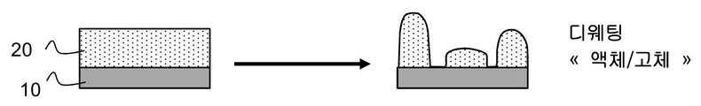
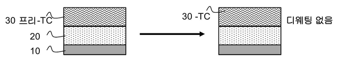
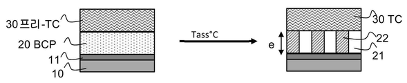
- 238000009736 wetting Methods 0.000 claims description 7
- PPBRXRYQALVLMV-UHFFFAOYSA-N Styrene Chemical compound C=CC1=CC=CC=C1 PPBRXRYQALVLMV-UHFFFAOYSA-N 0.000 claims description 6
- NIXOWILDQLNWCW-UHFFFAOYSA-N acrylic acid group Chemical group C(C=C)(=O)O NIXOWILDQLNWCW-UHFFFAOYSA-N 0.000 claims description 6
- 230000005494 condensation Effects 0.000 claims description 6
- 238000001312 dry etching Methods 0.000 claims description 6
- 229940116333 ethyl lactate Drugs 0.000 claims description 6
- 238000011065 in-situ storage Methods 0.000 claims description 6
- 239000012948 isocyanate Substances 0.000 claims description 6
- 150000002513 isocyanates Chemical class 0.000 claims description 6
- 230000003287 optical effect Effects 0.000 claims description 6
- DBSABEYSGXPBTA-RXSVEWSESA-N (2r)-2-[(1s)-1,2-dihydroxyethyl]-3,4-dihydroxy-2h-furan-5-one;phosphoric acid Chemical compound OP(O)(O)=O.OC[C@H](O)[C@H]1OC(=O)C(O)=C1O DBSABEYSGXPBTA-RXSVEWSESA-N 0.000 claims description 5
- BYEAHWXPCBROCE-UHFFFAOYSA-N 1,1,1,3,3,3-hexafluoropropan-2-ol Chemical compound FC(F)(F)C(O)C(F)(F)F BYEAHWXPCBROCE-UHFFFAOYSA-N 0.000 claims description 5
- FALRKNHUBBKYCC-UHFFFAOYSA-N 2-(chloromethyl)pyridine-3-carbonitrile Chemical compound ClCC1=NC=CC=C1C#N FALRKNHUBBKYCC-UHFFFAOYSA-N 0.000 claims description 5
- DKIDEFUBRARXTE-UHFFFAOYSA-M 3-mercaptopropionate Chemical compound [O-]C(=O)CCS DKIDEFUBRARXTE-UHFFFAOYSA-M 0.000 claims description 5
- QGZKDVFQNNGYKY-UHFFFAOYSA-O Ammonium Chemical compound [NH4+] QGZKDVFQNNGYKY-UHFFFAOYSA-O 0.000 claims description 5
- NVXLIZQNSVLKPO-UHFFFAOYSA-N Glucosereductone Chemical compound O=CC(O)C=O NVXLIZQNSVLKPO-UHFFFAOYSA-N 0.000 claims description 5
- FXHOOIRPVKKKFG-UHFFFAOYSA-N N,N-Dimethylacetamide Chemical compound CN(C)C(C)=O FXHOOIRPVKKKFG-UHFFFAOYSA-N 0.000 claims description 5
- LEHOTFFKMJEONL-UHFFFAOYSA-N Uric Acid Chemical compound N1C(=O)NC(=O)C2=C1NC(=O)N2 LEHOTFFKMJEONL-UHFFFAOYSA-N 0.000 claims description 5
- TVWHNULVHGKJHS-UHFFFAOYSA-N Uric acid Natural products N1C(=O)NC(=O)C2NC(=O)NC21 TVWHNULVHGKJHS-UHFFFAOYSA-N 0.000 claims description 5
- 150000008065 acid anhydrides Chemical class 0.000 claims description 5
- 150000007513 acids Chemical class 0.000 claims description 5
- 125000000129 anionic group Chemical group 0.000 claims description 5
- 229940071097 ascorbyl phosphate Drugs 0.000 claims description 5
- RHDGNLCLDBVESU-UHFFFAOYSA-N but-3-en-4-olide Chemical compound O=C1CC=CO1 RHDGNLCLDBVESU-UHFFFAOYSA-N 0.000 claims description 5
- 150000002009 diols Chemical class 0.000 claims description 5
- 150000002460 imidazoles Chemical class 0.000 claims description 5
- 238000001459 lithography Methods 0.000 claims description 5
- 230000001404 mediated effect Effects 0.000 claims description 5
- 239000012528 membrane Substances 0.000 claims description 5
- 230000003472 neutralizing effect Effects 0.000 claims description 5
- NFHFRUOZVGFOOS-UHFFFAOYSA-N palladium;triphenylphosphane Chemical compound [Pd].C1=CC=CC=C1P(C=1C=CC=CC=1)C1=CC=CC=C1.C1=CC=CC=C1P(C=1C=CC=CC=1)C1=CC=CC=C1.C1=CC=CC=C1P(C=1C=CC=CC=1)C1=CC=CC=C1.C1=CC=CC=C1P(C=1C=CC=CC=1)C1=CC=CC=C1 NFHFRUOZVGFOOS-UHFFFAOYSA-N 0.000 claims description 5
- 238000001020 plasma etching Methods 0.000 claims description 5
- 150000008442 polyphenolic compounds Chemical class 0.000 claims description 5
- 235000013824 polyphenols Nutrition 0.000 claims description 5
- 230000005855 radiation Effects 0.000 claims description 5
- 239000011877 solvent mixture Substances 0.000 claims description 5
- 229940014800 succinic anhydride Drugs 0.000 claims description 5
- ITMCEJHCFYSIIV-UHFFFAOYSA-M triflate Chemical compound [O-]S(=O)(=O)C(F)(F)F ITMCEJHCFYSIIV-UHFFFAOYSA-M 0.000 claims description 5
- 229940116269 uric acid Drugs 0.000 claims description 5
- HBAQYPYDRFILMT-UHFFFAOYSA-N 8-[3-(1-cyclopropylpyrazol-4-yl)-1H-pyrazolo[4,3-d]pyrimidin-5-yl]-3-methyl-3,8-diazabicyclo[3.2.1]octan-2-one Chemical class C1(CC1)N1N=CC(=C1)C1=NNC2=C1N=C(N=C2)N1C2C(N(CC1CC2)C)=O HBAQYPYDRFILMT-UHFFFAOYSA-N 0.000 claims description 4
- 229920001730 Moisture cure polyurethane Polymers 0.000 claims description 4
- 230000002378 acidificating effect Effects 0.000 claims description 4
- 150000001350 alkyl halides Chemical class 0.000 claims description 4
- 235000010323 ascorbic acid Nutrition 0.000 claims description 4
- 239000011668 ascorbic acid Substances 0.000 claims description 4
- 229960005070 ascorbic acid Drugs 0.000 claims description 4
- 229910052799 carbon Inorganic materials 0.000 claims description 4
- 125000003636 chemical group Chemical group 0.000 claims description 4
- 239000003638 chemical reducing agent Substances 0.000 claims description 4
- 238000000576 coating method Methods 0.000 claims description 4
- 238000009472 formulation Methods 0.000 claims description 4
- 229910021389 graphene Inorganic materials 0.000 claims description 4
- 150000002429 hydrazines Chemical class 0.000 claims description 4
- 239000007943 implant Substances 0.000 claims description 4
- 150000002734 metacrylic acid derivatives Chemical class 0.000 claims description 4
- 238000004377 microelectronic Methods 0.000 claims description 4
- 230000005693 optoelectronics Effects 0.000 claims description 4
- 150000001451 organic peroxides Chemical class 0.000 claims description 4
- 230000008520 organization Effects 0.000 claims description 4
- 239000003973 paint Substances 0.000 claims description 4
- 150000003839 salts Chemical class 0.000 claims description 4
- PSGCQDPCAWOCSH-UHFFFAOYSA-N (4,7,7-trimethyl-3-bicyclo[2.2.1]heptanyl) prop-2-enoate Chemical compound C1CC2(C)C(OC(=O)C=C)CC1C2(C)C PSGCQDPCAWOCSH-UHFFFAOYSA-N 0.000 claims description 3
- BGJSXRVXTHVRSN-UHFFFAOYSA-N 1,3,5-trioxane Chemical compound C1OCOCO1 BGJSXRVXTHVRSN-UHFFFAOYSA-N 0.000 claims description 3
- PHPRWKJDGHSJMI-UHFFFAOYSA-N 1-adamantyl prop-2-enoate Chemical compound C1C(C2)CC3CC2CC1(OC(=O)C=C)C3 PHPRWKJDGHSJMI-UHFFFAOYSA-N 0.000 claims description 3
- OXBLVCZKDOZZOJ-UHFFFAOYSA-N 2,3-Dihydrothiophene Chemical compound C1CC=CS1 OXBLVCZKDOZZOJ-UHFFFAOYSA-N 0.000 claims description 3
- JECYNCQXXKQDJN-UHFFFAOYSA-N 2-(2-methylhexan-2-yloxymethyl)oxirane Chemical compound CCCCC(C)(C)OCC1CO1 JECYNCQXXKQDJN-UHFFFAOYSA-N 0.000 claims description 3
- IQDPHMACOQAPBQ-UHFFFAOYSA-N 2-ethoxyethyl 2-cyanoprop-2-enoate Chemical compound CCOCCOC(=O)C(=C)C#N IQDPHMACOQAPBQ-UHFFFAOYSA-N 0.000 claims description 3
- KBKNKFIRGXQLDB-UHFFFAOYSA-N 2-fluoroethenylbenzene Chemical compound FC=CC1=CC=CC=C1 KBKNKFIRGXQLDB-UHFFFAOYSA-N 0.000 claims description 3
- IEJYPTHGJFYJPV-UHFFFAOYSA-N 3,3,3-trifluoropropyl 2-cyanoprop-2-enoate Chemical compound FC(F)(F)CCOC(=O)C(=C)C#N IEJYPTHGJFYJPV-UHFFFAOYSA-N 0.000 claims description 3
- GSVKAZKMKQOQGZ-UHFFFAOYSA-N C(#N)C(C(=O)OC1=C(C=CC=C1)CC)=C Chemical compound C(#N)C(C(=O)OC1=C(C=CC=C1)CC)=C GSVKAZKMKQOQGZ-UHFFFAOYSA-N 0.000 claims description 3
- BVKZGUZCCUSVTD-UHFFFAOYSA-L Carbonate Chemical compound [O-]C([O-])=O BVKZGUZCCUSVTD-UHFFFAOYSA-L 0.000 claims description 3
- PXGOKWXKJXAPGV-UHFFFAOYSA-N Fluorine Chemical compound FF PXGOKWXKJXAPGV-UHFFFAOYSA-N 0.000 claims description 3
- BLRPTPMANUNPDV-UHFFFAOYSA-N Silane Chemical compound [SiH4] BLRPTPMANUNPDV-UHFFFAOYSA-N 0.000 claims description 3
- QYKIQEUNHZKYBP-UHFFFAOYSA-N Vinyl ether Chemical compound C=COC=C QYKIQEUNHZKYBP-UHFFFAOYSA-N 0.000 claims description 3
- 150000001252 acrylic acid derivatives Chemical class 0.000 claims description 3
- 239000005456 alcohol based solvent Substances 0.000 claims description 3
- 150000001299 aldehydes Chemical class 0.000 claims description 3
- 125000001931 aliphatic group Chemical group 0.000 claims description 3
- 125000005250 alkyl acrylate group Chemical group 0.000 claims description 3
- 150000001454 anthracenes Chemical class 0.000 claims description 3
- 239000003963 antioxidant agent Substances 0.000 claims description 3
- 235000006708 antioxidants Nutrition 0.000 claims description 3
- 125000003118 aryl group Chemical group 0.000 claims description 3
- 125000004432 carbon atom Chemical group C* 0.000 claims description 3
- 238000009833 condensation Methods 0.000 claims description 3
- 125000004386 diacrylate group Chemical group 0.000 claims description 3
- JJJFUHOGVZWXNQ-UHFFFAOYSA-N enbucrilate Chemical compound CCCCOC(=O)C(=C)C#N JJJFUHOGVZWXNQ-UHFFFAOYSA-N 0.000 claims description 3
- 229950010048 enbucrilate Drugs 0.000 claims description 3
- 150000002148 esters Chemical class 0.000 claims description 3
- FGBJXOREULPLGL-UHFFFAOYSA-N ethyl cyanoacrylate Chemical compound CCOC(=O)C(=C)C#N FGBJXOREULPLGL-UHFFFAOYSA-N 0.000 claims description 3
- 229940053009 ethyl cyanoacrylate Drugs 0.000 claims description 3
- 239000012530 fluid Substances 0.000 claims description 3
- 229910052731 fluorine Inorganic materials 0.000 claims description 3
- 239000011737 fluorine Substances 0.000 claims description 3
- ZYMKZMDQUPCXRP-UHFFFAOYSA-N fluoro prop-2-enoate Chemical compound FOC(=O)C=C ZYMKZMDQUPCXRP-UHFFFAOYSA-N 0.000 claims description 3
- XUCNUKMRBVNAPB-UHFFFAOYSA-N fluoroethene Chemical compound FC=C XUCNUKMRBVNAPB-UHFFFAOYSA-N 0.000 claims description 3
- 229910052732 germanium Inorganic materials 0.000 claims description 3
- GNPVGFCGXDBREM-UHFFFAOYSA-N germanium atom Chemical group [Ge] GNPVGFCGXDBREM-UHFFFAOYSA-N 0.000 claims description 3
- 125000004356 hydroxy functional group Chemical group O* 0.000 claims description 3
- 230000000977 initiatory effect Effects 0.000 claims description 3
- 239000000976 ink Substances 0.000 claims description 3
- MGFYSGNNHQQTJW-UHFFFAOYSA-N iodonium Chemical compound [IH2+] MGFYSGNNHQQTJW-UHFFFAOYSA-N 0.000 claims description 3
- 229940119545 isobornyl methacrylate Drugs 0.000 claims description 3
- 150000002576 ketones Chemical class 0.000 claims description 3
- 150000003951 lactams Chemical class 0.000 claims description 3
- 150000002596 lactones Chemical class 0.000 claims description 3
- 150000002689 maleic acids Chemical class 0.000 claims description 3
- 125000002950 monocyclic group Chemical group 0.000 claims description 3
- 150000002848 norbornenes Chemical class 0.000 claims description 3
- ZRZKTJRBDZGDOG-UHFFFAOYSA-N octadecyl 2-cyanoprop-2-enoate Chemical compound CCCCCCCCCCCCCCCCCCOC(=O)C(=C)C#N ZRZKTJRBDZGDOG-UHFFFAOYSA-N 0.000 claims description 3
- RPQUGMLCZLGZTG-UHFFFAOYSA-N octyl cyanoacrylate Chemical compound CCCCCCCCOC(=O)C(=C)C#N RPQUGMLCZLGZTG-UHFFFAOYSA-N 0.000 claims description 3
- 150000001282 organosilanes Chemical class 0.000 claims description 3
- 239000005022 packaging material Substances 0.000 claims description 3
- 150000004714 phosphonium salts Chemical class 0.000 claims description 3
- 239000004014 plasticizer Substances 0.000 claims description 3
- 229920001228 polyisocyanate Polymers 0.000 claims description 3
- 239000005056 polyisocyanate Substances 0.000 claims description 3
- 229920001296 polysiloxane Polymers 0.000 claims description 3
- 229910000077 silane Inorganic materials 0.000 claims description 3
- 230000000638 stimulation Effects 0.000 claims description 3
- LVLANIHJQRZTPY-UHFFFAOYSA-N vinyl carbamate Chemical class NC(=O)OC=C LVLANIHJQRZTPY-UHFFFAOYSA-N 0.000 claims description 3
- 239000000080 wetting agent Substances 0.000 claims description 3
- 125000001971 neopentyl group Chemical group [H]C([*])([H])C(C([H])([H])[H])(C([H])([H])[H])C([H])([H])[H] 0.000 claims description 2
- 125000000466 oxiranyl group Chemical group 0.000 claims description 2
- VOVUARRWDCVURC-UHFFFAOYSA-N thiirane Chemical compound C1CS1 VOVUARRWDCVURC-UHFFFAOYSA-N 0.000 claims description 2
- RTZKZFJDLAIYFH-UHFFFAOYSA-N Diethyl ether Chemical compound CCOCC RTZKZFJDLAIYFH-UHFFFAOYSA-N 0.000 claims 2
- 125000004122 cyclic group Chemical group 0.000 claims 1
- 150000002118 epoxides Chemical class 0.000 claims 1
- QEWYKACRFQMRMB-UHFFFAOYSA-M fluoroacetate Chemical compound [O-]C(=O)CF QEWYKACRFQMRMB-UHFFFAOYSA-M 0.000 claims 1
- 150000002238 fumaric acids Chemical class 0.000 claims 1
- 125000005641 methacryl group Chemical group 0.000 claims 1
- 150000002825 nitriles Chemical class 0.000 claims 1
- 150000003460 sulfonic acids Chemical class 0.000 claims 1
- 238000002203 pretreatment Methods 0.000 abstract 1
- 239000010408 film Substances 0.000 description 66
- 239000000243 solution Substances 0.000 description 41
- 238000004528 spin coating Methods 0.000 description 26
- 238000002408 directed self-assembly Methods 0.000 description 17
- 239000004793 Polystyrene Substances 0.000 description 14
- IJGRMHOSHXDMSA-UHFFFAOYSA-N Atomic nitrogen Chemical compound N#N IJGRMHOSHXDMSA-UHFFFAOYSA-N 0.000 description 12
- LLHKCFNBLRBOGN-UHFFFAOYSA-N propylene glycol methyl ether acetate Chemical compound COCC(C)OC(C)=O LLHKCFNBLRBOGN-UHFFFAOYSA-N 0.000 description 11
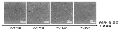
- 238000004626 scanning electron microscopy Methods 0.000 description 11
- 238000009792 diffusion process Methods 0.000 description 9
- OZAIFHULBGXAKX-UHFFFAOYSA-N 2-(2-cyanopropan-2-yldiazenyl)-2-methylpropanenitrile Chemical compound N#CC(C)(C)N=NC(C)(C)C#N OZAIFHULBGXAKX-UHFFFAOYSA-N 0.000 description 8
- 229920001519 homopolymer Polymers 0.000 description 8
- 230000003993 interaction Effects 0.000 description 7
- 238000002156 mixing Methods 0.000 description 7
- 229910052757 nitrogen Inorganic materials 0.000 description 7
- 239000013557 residual solvent Substances 0.000 description 7
- 229920006301 statistical copolymer Polymers 0.000 description 7
- NTIZESTWPVYFNL-UHFFFAOYSA-N Methyl isobutyl ketone Chemical compound CC(C)CC(C)=O NTIZESTWPVYFNL-UHFFFAOYSA-N 0.000 description 6
- UIHCLUNTQKBZGK-UHFFFAOYSA-N Methyl isobutyl ketone Natural products CCC(C)C(C)=O UIHCLUNTQKBZGK-UHFFFAOYSA-N 0.000 description 6
- 125000003055 glycidyl group Chemical group C(C1CO1)* 0.000 description 6
- 229920006254 polymer film Polymers 0.000 description 6
- 238000003786 synthesis reaction Methods 0.000 description 6
- 229920002818 (Hydroxyethyl)methacrylate Polymers 0.000 description 5
- 238000009826 distribution Methods 0.000 description 5
- 230000000694 effects Effects 0.000 description 5
- 238000003384 imaging method Methods 0.000 description 5
- ZDYVRSLAEXCVBX-UHFFFAOYSA-N pyridinium p-toluenesulfonate Chemical compound C1=CC=[NH+]C=C1.CC1=CC=C(S([O-])(=O)=O)C=C1 ZDYVRSLAEXCVBX-UHFFFAOYSA-N 0.000 description 5
- 241000894007 species Species 0.000 description 5
- 235000012431 wafers Nutrition 0.000 description 5
- VZCYOOQTPOCHFL-OWOJBTEDSA-N Fumaric acid Chemical compound OC(=O)\C=C\C(O)=O VZCYOOQTPOCHFL-OWOJBTEDSA-N 0.000 description 4
- 229920000028 Gradient copolymer Polymers 0.000 description 4
- JUJWROOIHBZHMG-UHFFFAOYSA-N Pyridine Chemical class C1=CC=NC=C1 JUJWROOIHBZHMG-UHFFFAOYSA-N 0.000 description 4
- 239000012298 atmosphere Substances 0.000 description 4
- 150000005829 chemical entities Chemical class 0.000 description 4
- 239000013078 crystal Substances 0.000 description 4
- 239000007789 gas Substances 0.000 description 4
- 239000001257 hydrogen Substances 0.000 description 4
- 229910052739 hydrogen Inorganic materials 0.000 description 4
- 150000002924 oxiranes Chemical class 0.000 description 4
- 229920001343 polytetrafluoroethylene Polymers 0.000 description 4
- 239000004810 polytetrafluoroethylene Substances 0.000 description 4
- 238000012545 processing Methods 0.000 description 4
- 230000007928 solubilization Effects 0.000 description 4
- 238000005063 solubilization Methods 0.000 description 4
- 241000446313 Lamella Species 0.000 description 3
- 239000002671 adjuvant Substances 0.000 description 3
- 150000001298 alcohols Chemical class 0.000 description 3
- 238000004458 analytical method Methods 0.000 description 3
- 230000015572 biosynthetic process Effects 0.000 description 3
- 230000008859 change Effects 0.000 description 3
- 239000007809 chemical reaction catalyst Substances 0.000 description 3
- 230000007547 defect Effects 0.000 description 3
- 230000006866 deterioration Effects 0.000 description 3
- 238000010586 diagram Methods 0.000 description 3
- 239000000428 dust Substances 0.000 description 3
- 238000001704 evaporation Methods 0.000 description 3
- 238000000605 extraction Methods 0.000 description 3
- VOZRXNHHFUQHIL-UHFFFAOYSA-N glycidyl methacrylate Chemical compound CC(=C)C(=O)OCC1CO1 VOZRXNHHFUQHIL-UHFFFAOYSA-N 0.000 description 3
- 239000003999 initiator Substances 0.000 description 3
- 239000011572 manganese Substances 0.000 description 3
- 239000002245 particle Substances 0.000 description 3
- 238000005191 phase separation Methods 0.000 description 3
- 239000002861 polymer material Substances 0.000 description 3
- 238000002360 preparation method Methods 0.000 description 3
- 238000001338 self-assembly Methods 0.000 description 3
- ODHXBMXNKOYIBV-UHFFFAOYSA-N triphenylamine Chemical compound C1=CC=CC=C1N(C=1C=CC=CC=1)C1=CC=CC=C1 ODHXBMXNKOYIBV-UHFFFAOYSA-N 0.000 description 3
- QTKPMCIBUROOGY-UHFFFAOYSA-N 2,2,2-trifluoroethyl 2-methylprop-2-enoate Chemical compound CC(=C)C(=O)OCC(F)(F)F QTKPMCIBUROOGY-UHFFFAOYSA-N 0.000 description 2
- QGZKDVFQNNGYKY-UHFFFAOYSA-N Ammonia Chemical compound N QGZKDVFQNNGYKY-UHFFFAOYSA-N 0.000 description 2
- IAYPIBMASNFSPL-UHFFFAOYSA-N Ethylene oxide Chemical group C1CO1 IAYPIBMASNFSPL-UHFFFAOYSA-N 0.000 description 2
- OAKJQQAXSVQMHS-UHFFFAOYSA-N Hydrazine Chemical compound NN OAKJQQAXSVQMHS-UHFFFAOYSA-N 0.000 description 2
- 238000006845 Michael addition reaction Methods 0.000 description 2
- 229920005603 alternating copolymer Polymers 0.000 description 2
- 230000003321 amplification Effects 0.000 description 2
- 238000013459 approach Methods 0.000 description 2
- 239000007864 aqueous solution Substances 0.000 description 2
- 230000008901 benefit Effects 0.000 description 2
- 238000007796 conventional method Methods 0.000 description 2
- 150000004292 cyclic ethers Chemical class 0.000 description 2
- 238000006731 degradation reaction Methods 0.000 description 2
- 230000001419 dependent effect Effects 0.000 description 2
- 229920001971 elastomer Polymers 0.000 description 2
- 238000000572 ellipsometry Methods 0.000 description 2
- 230000008020 evaporation Effects 0.000 description 2
- 238000002474 experimental method Methods 0.000 description 2
- 239000001530 fumaric acid Substances 0.000 description 2
- 230000005484 gravity Effects 0.000 description 2
- 150000002500 ions Chemical class 0.000 description 2
- 230000007246 mechanism Effects 0.000 description 2
- 229910052751 metal Inorganic materials 0.000 description 2
- 239000002184 metal Substances 0.000 description 2
- 238000003199 nucleic acid amplification method Methods 0.000 description 2
- BASFCYQUMIYNBI-UHFFFAOYSA-N platinum Chemical compound [Pt] BASFCYQUMIYNBI-UHFFFAOYSA-N 0.000 description 2
- 239000003880 polar aprotic solvent Substances 0.000 description 2
- 229920002223 polystyrene Polymers 0.000 description 2
- 229920005604 random copolymer Polymers 0.000 description 2
- 230000009257 reactivity Effects 0.000 description 2
- 230000003381 solubilizing effect Effects 0.000 description 2
- 238000010561 standard procedure Methods 0.000 description 2
- 238000003860 storage Methods 0.000 description 2
- 150000003457 sulfones Chemical class 0.000 description 2
- 229920001187 thermosetting polymer Polymers 0.000 description 2
- 239000010409 thin film Substances 0.000 description 2
- VZCYOOQTPOCHFL-UHFFFAOYSA-N trans-butenedioic acid Natural products OC(=O)C=CC(O)=O VZCYOOQTPOCHFL-UHFFFAOYSA-N 0.000 description 2
- YNLJHXFENQDVSS-UHFFFAOYSA-N 2,2-dimethylpropyl 2-cyanoprop-2-enoate Chemical compound CC(C)(C)COC(=O)C(=C)C#N YNLJHXFENQDVSS-UHFFFAOYSA-N 0.000 description 1
- VHUUQVKOLVNVRT-UHFFFAOYSA-N Ammonium hydroxide Chemical compound [NH4+].[OH-] VHUUQVKOLVNVRT-UHFFFAOYSA-N 0.000 description 1
- 208000037170 Delayed Emergence from Anesthesia Diseases 0.000 description 1
- UFHFLCQGNIYNRP-UHFFFAOYSA-N Hydrogen Chemical compound [H][H] UFHFLCQGNIYNRP-UHFFFAOYSA-N 0.000 description 1
- WOBHKFSMXKNTIM-UHFFFAOYSA-N Hydroxyethyl methacrylate Chemical compound CC(=C)C(=O)OCCO WOBHKFSMXKNTIM-UHFFFAOYSA-N 0.000 description 1
- PWHULOQIROXLJO-UHFFFAOYSA-N Manganese Chemical compound [Mn] PWHULOQIROXLJO-UHFFFAOYSA-N 0.000 description 1
- ISWSIDIOOBJBQZ-UHFFFAOYSA-N Phenol Chemical compound OC1=CC=CC=C1 ISWSIDIOOBJBQZ-UHFFFAOYSA-N 0.000 description 1
- 230000001133 acceleration Effects 0.000 description 1
- 239000003929 acidic solution Substances 0.000 description 1
- 230000009471 action Effects 0.000 description 1
- 238000001994 activation Methods 0.000 description 1
- 230000004913 activation Effects 0.000 description 1
- 230000000996 additive effect Effects 0.000 description 1
- 239000000443 aerosol Substances 0.000 description 1
- 229910021529 ammonia Inorganic materials 0.000 description 1
- 239000000908 ammonium hydroxide Substances 0.000 description 1
- 238000004873 anchoring Methods 0.000 description 1
- 238000010539 anionic addition polymerization reaction Methods 0.000 description 1
- 230000003078 antioxidant effect Effects 0.000 description 1
- QVGXLLKOCUKJST-UHFFFAOYSA-N atomic oxygen Chemical compound [O] QVGXLLKOCUKJST-UHFFFAOYSA-N 0.000 description 1
- 239000003637 basic solution Substances 0.000 description 1
- 238000004364 calculation method Methods 0.000 description 1
- 230000015556 catabolic process Effects 0.000 description 1
- 230000003197 catalytic effect Effects 0.000 description 1
- 238000005229 chemical vapour deposition Methods 0.000 description 1
- 238000004320 controlled atmosphere Methods 0.000 description 1
- 238000012937 correction Methods 0.000 description 1
- 229920006037 cross link polymer Polymers 0.000 description 1
- 238000000354 decomposition reaction Methods 0.000 description 1
- 230000007812 deficiency Effects 0.000 description 1
- 230000003111 delayed effect Effects 0.000 description 1
- 238000011161 development Methods 0.000 description 1
- 150000004985 diamines Chemical class 0.000 description 1
- 208000037265 diseases, disorders, signs and symptoms Diseases 0.000 description 1
- 239000006185 dispersion Substances 0.000 description 1
- 238000004090 dissolution Methods 0.000 description 1
- 230000002708 enhancing effect Effects 0.000 description 1
- 125000004185 ester group Chemical group 0.000 description 1
- 125000001495 ethyl group Chemical group [H]C([H])([H])C([H])([H])* 0.000 description 1
- 238000002270 exclusion chromatography Methods 0.000 description 1
- 125000001153 fluoro group Chemical group F* 0.000 description 1
- 125000003784 fluoroethyl group Chemical group [H]C([H])(F)C([H])([H])* 0.000 description 1
- 238000007306 functionalization reaction Methods 0.000 description 1
- 230000036541 health Effects 0.000 description 1
- 125000004836 hexamethylene group Chemical group [H]C([H])([*:2])C([H])([H])C([H])([H])C([H])([H])C([H])([H])C([H])([H])[*:1] 0.000 description 1
- 125000002887 hydroxy group Chemical group [H]O* 0.000 description 1
- 125000002768 hydroxyalkyl group Chemical group 0.000 description 1
- 238000003711 image thresholding Methods 0.000 description 1
- 239000012535 impurity Substances 0.000 description 1
- 238000009616 inductively coupled plasma Methods 0.000 description 1
- 238000002329 infrared spectrum Methods 0.000 description 1
- 239000011872 intimate mixture Substances 0.000 description 1
- 238000010884 ion-beam technique Methods 0.000 description 1
- 239000011344 liquid material Substances 0.000 description 1
- 210000003141 lower extremity Anatomy 0.000 description 1
- 229940074358 magnesium ascorbate Drugs 0.000 description 1
- AIOKQVJVNPDJKA-ZZMNMWMASA-L magnesium;(2r)-2-[(1s)-1,2-dihydroxyethyl]-4-hydroxy-5-oxo-2h-furan-3-olate Chemical compound [Mg+2].OC[C@H](O)[C@H]1OC(=O)C(O)=C1[O-].OC[C@H](O)[C@H]1OC(=O)C(O)=C1[O-] AIOKQVJVNPDJKA-ZZMNMWMASA-L 0.000 description 1
- VZCYOOQTPOCHFL-UPHRSURJSA-N maleic acid Chemical group OC(=O)\C=C/C(O)=O VZCYOOQTPOCHFL-UPHRSURJSA-N 0.000 description 1
- 229910052748 manganese Inorganic materials 0.000 description 1
- 239000002086 nanomaterial Substances 0.000 description 1
- 238000006386 neutralization reaction Methods 0.000 description 1
- JFNLZVQOOSMTJK-KNVOCYPGSA-N norbornene Chemical compound C1[C@@H]2CC[C@H]1C=C2 JFNLZVQOOSMTJK-KNVOCYPGSA-N 0.000 description 1
- 230000006911 nucleation Effects 0.000 description 1
- 238000010899 nucleation Methods 0.000 description 1
- TWNQGVIAIRXVLR-UHFFFAOYSA-N oxo(oxoalumanyloxy)alumane Chemical compound O=[Al]O[Al]=O TWNQGVIAIRXVLR-UHFFFAOYSA-N 0.000 description 1
- FNVQIYPKWVVQID-UHFFFAOYSA-N oxolan-2-ylmethyl 2-cyanoprop-2-enoate Chemical compound N#CC(=C)C(=O)OCC1CCCO1 FNVQIYPKWVVQID-UHFFFAOYSA-N 0.000 description 1
- 239000001301 oxygen Substances 0.000 description 1
- 229910052760 oxygen Inorganic materials 0.000 description 1
- 238000002161 passivation Methods 0.000 description 1
- 238000000206 photolithography Methods 0.000 description 1
- 229910052697 platinum Inorganic materials 0.000 description 1
- 229920003229 poly(methyl methacrylate) Polymers 0.000 description 1
- 229920000193 polymethacrylate Polymers 0.000 description 1
- 239000004926 polymethyl methacrylate Substances 0.000 description 1
- ULWHHBHJGPPBCO-UHFFFAOYSA-N propane-1,1-diol Chemical compound CCC(O)O ULWHHBHJGPPBCO-UHFFFAOYSA-N 0.000 description 1
- 238000000425 proton nuclear magnetic resonance spectrum Methods 0.000 description 1
- 238000003908 quality control method Methods 0.000 description 1
- 230000035484 reaction time Effects 0.000 description 1
- 230000009467 reduction Effects 0.000 description 1
- 238000009877 rendering Methods 0.000 description 1
- 238000001878 scanning electron micrograph Methods 0.000 description 1
- 238000001350 scanning transmission electron microscopy Methods 0.000 description 1
- 238000005204 segregation Methods 0.000 description 1
- 238000010187 selection method Methods 0.000 description 1
- 239000004065 semiconductor Substances 0.000 description 1
- 238000000926 separation method Methods 0.000 description 1
- 150000003384 small molecules Chemical class 0.000 description 1
- 239000012453 solvate Substances 0.000 description 1
- 238000001228 spectrum Methods 0.000 description 1
- 238000001330 spinodal decomposition reaction Methods 0.000 description 1
- 230000006641 stabilisation Effects 0.000 description 1
- 238000011105 stabilization Methods 0.000 description 1
- 230000000087 stabilizing effect Effects 0.000 description 1
- 230000002194 synthesizing effect Effects 0.000 description 1
- 238000007725 thermal activation Methods 0.000 description 1
- 238000012719 thermal polymerization Methods 0.000 description 1
- 230000007704 transition Effects 0.000 description 1
- 239000011345 viscous material Substances 0.000 description 1
- 238000005406 washing Methods 0.000 description 1
- 238000013316 zoning Methods 0.000 description 1
Images


Classifications
-
- G—PHYSICS
- G03—PHOTOGRAPHY; CINEMATOGRAPHY; ANALOGOUS TECHNIQUES USING WAVES OTHER THAN OPTICAL WAVES; ELECTROGRAPHY; HOLOGRAPHY
- G03F—PHOTOMECHANICAL PRODUCTION OF TEXTURED OR PATTERNED SURFACES, e.g. FOR PRINTING, FOR PROCESSING OF SEMICONDUCTOR DEVICES; MATERIALS THEREFOR; ORIGINALS THEREFOR; APPARATUS SPECIALLY ADAPTED THEREFOR
- G03F7/00—Photomechanical, e.g. photolithographic, production of textured or patterned surfaces, e.g. printing surfaces; Materials therefor, e.g. comprising photoresists; Apparatus specially adapted therefor
- G03F7/0002—Lithographic processes using patterning methods other than those involving the exposure to radiation, e.g. by stamping
-
- G—PHYSICS
- G03—PHOTOGRAPHY; CINEMATOGRAPHY; ANALOGOUS TECHNIQUES USING WAVES OTHER THAN OPTICAL WAVES; ELECTROGRAPHY; HOLOGRAPHY
- G03F—PHOTOMECHANICAL PRODUCTION OF TEXTURED OR PATTERNED SURFACES, e.g. FOR PRINTING, FOR PROCESSING OF SEMICONDUCTOR DEVICES; MATERIALS THEREFOR; ORIGINALS THEREFOR; APPARATUS SPECIALLY ADAPTED THEREFOR
- G03F7/00—Photomechanical, e.g. photolithographic, production of textured or patterned surfaces, e.g. printing surfaces; Materials therefor, e.g. comprising photoresists; Apparatus specially adapted therefor
- G03F7/004—Photosensitive materials
- G03F7/09—Photosensitive materials characterised by structural details, e.g. supports, auxiliary layers
- G03F7/095—Photosensitive materials characterised by structural details, e.g. supports, auxiliary layers having more than one photosensitive layer
-
- G—PHYSICS
- G03—PHOTOGRAPHY; CINEMATOGRAPHY; ANALOGOUS TECHNIQUES USING WAVES OTHER THAN OPTICAL WAVES; ELECTROGRAPHY; HOLOGRAPHY
- G03F—PHOTOMECHANICAL PRODUCTION OF TEXTURED OR PATTERNED SURFACES, e.g. FOR PRINTING, FOR PROCESSING OF SEMICONDUCTOR DEVICES; MATERIALS THEREFOR; ORIGINALS THEREFOR; APPARATUS SPECIALLY ADAPTED THEREFOR
- G03F1/00—Originals for photomechanical production of textured or patterned surfaces, e.g., masks, photo-masks, reticles; Mask blanks or pellicles therefor; Containers specially adapted therefor; Preparation thereof
- G03F1/38—Masks having auxiliary features, e.g. special coatings or marks for alignment or testing; Preparation thereof
- G03F1/48—Protective coatings
-
- C—CHEMISTRY; METALLURGY
- C08—ORGANIC MACROMOLECULAR COMPOUNDS; THEIR PREPARATION OR CHEMICAL WORKING-UP; COMPOSITIONS BASED THEREON
- C08F—MACROMOLECULAR COMPOUNDS OBTAINED BY REACTIONS ONLY INVOLVING CARBON-TO-CARBON UNSATURATED BONDS
- C08F287/00—Macromolecular compounds obtained by polymerising monomers on to block polymers
-
- G—PHYSICS
- G03—PHOTOGRAPHY; CINEMATOGRAPHY; ANALOGOUS TECHNIQUES USING WAVES OTHER THAN OPTICAL WAVES; ELECTROGRAPHY; HOLOGRAPHY
- G03F—PHOTOMECHANICAL PRODUCTION OF TEXTURED OR PATTERNED SURFACES, e.g. FOR PRINTING, FOR PROCESSING OF SEMICONDUCTOR DEVICES; MATERIALS THEREFOR; ORIGINALS THEREFOR; APPARATUS SPECIALLY ADAPTED THEREFOR
- G03F1/00—Originals for photomechanical production of textured or patterned surfaces, e.g., masks, photo-masks, reticles; Mask blanks or pellicles therefor; Containers specially adapted therefor; Preparation thereof
- G03F1/68—Preparation processes not covered by groups G03F1/20 - G03F1/50
- G03F1/80—Etching
-
- G—PHYSICS
- G03—PHOTOGRAPHY; CINEMATOGRAPHY; ANALOGOUS TECHNIQUES USING WAVES OTHER THAN OPTICAL WAVES; ELECTROGRAPHY; HOLOGRAPHY
- G03F—PHOTOMECHANICAL PRODUCTION OF TEXTURED OR PATTERNED SURFACES, e.g. FOR PRINTING, FOR PROCESSING OF SEMICONDUCTOR DEVICES; MATERIALS THEREFOR; ORIGINALS THEREFOR; APPARATUS SPECIALLY ADAPTED THEREFOR
- G03F7/00—Photomechanical, e.g. photolithographic, production of textured or patterned surfaces, e.g. printing surfaces; Materials therefor, e.g. comprising photoresists; Apparatus specially adapted therefor
- G03F7/004—Photosensitive materials
- G03F7/0045—Photosensitive materials with organic non-macromolecular light-sensitive compounds not otherwise provided for, e.g. dissolution inhibitors
-
- G—PHYSICS
- G03—PHOTOGRAPHY; CINEMATOGRAPHY; ANALOGOUS TECHNIQUES USING WAVES OTHER THAN OPTICAL WAVES; ELECTROGRAPHY; HOLOGRAPHY
- G03F—PHOTOMECHANICAL PRODUCTION OF TEXTURED OR PATTERNED SURFACES, e.g. FOR PRINTING, FOR PROCESSING OF SEMICONDUCTOR DEVICES; MATERIALS THEREFOR; ORIGINALS THEREFOR; APPARATUS SPECIALLY ADAPTED THEREFOR
- G03F7/00—Photomechanical, e.g. photolithographic, production of textured or patterned surfaces, e.g. printing surfaces; Materials therefor, e.g. comprising photoresists; Apparatus specially adapted therefor
- G03F7/004—Photosensitive materials
- G03F7/027—Non-macromolecular photopolymerisable compounds having carbon-to-carbon double bonds, e.g. ethylenic compounds
- G03F7/028—Non-macromolecular photopolymerisable compounds having carbon-to-carbon double bonds, e.g. ethylenic compounds with photosensitivity-increasing substances, e.g. photoinitiators
-
- G—PHYSICS
- G03—PHOTOGRAPHY; CINEMATOGRAPHY; ANALOGOUS TECHNIQUES USING WAVES OTHER THAN OPTICAL WAVES; ELECTROGRAPHY; HOLOGRAPHY
- G03F—PHOTOMECHANICAL PRODUCTION OF TEXTURED OR PATTERNED SURFACES, e.g. FOR PRINTING, FOR PROCESSING OF SEMICONDUCTOR DEVICES; MATERIALS THEREFOR; ORIGINALS THEREFOR; APPARATUS SPECIALLY ADAPTED THEREFOR
- G03F7/00—Photomechanical, e.g. photolithographic, production of textured or patterned surfaces, e.g. printing surfaces; Materials therefor, e.g. comprising photoresists; Apparatus specially adapted therefor
- G03F7/004—Photosensitive materials
- G03F7/027—Non-macromolecular photopolymerisable compounds having carbon-to-carbon double bonds, e.g. ethylenic compounds
- G03F7/032—Non-macromolecular photopolymerisable compounds having carbon-to-carbon double bonds, e.g. ethylenic compounds with binders
- G03F7/033—Non-macromolecular photopolymerisable compounds having carbon-to-carbon double bonds, e.g. ethylenic compounds with binders the binders being polymers obtained by reactions only involving carbon-to-carbon unsaturated bonds, e.g. vinyl polymers
-
- G—PHYSICS
- G03—PHOTOGRAPHY; CINEMATOGRAPHY; ANALOGOUS TECHNIQUES USING WAVES OTHER THAN OPTICAL WAVES; ELECTROGRAPHY; HOLOGRAPHY
- G03F—PHOTOMECHANICAL PRODUCTION OF TEXTURED OR PATTERNED SURFACES, e.g. FOR PRINTING, FOR PROCESSING OF SEMICONDUCTOR DEVICES; MATERIALS THEREFOR; ORIGINALS THEREFOR; APPARATUS SPECIALLY ADAPTED THEREFOR
- G03F7/00—Photomechanical, e.g. photolithographic, production of textured or patterned surfaces, e.g. printing surfaces; Materials therefor, e.g. comprising photoresists; Apparatus specially adapted therefor
- G03F7/004—Photosensitive materials
- G03F7/038—Macromolecular compounds which are rendered insoluble or differentially wettable
-
- G—PHYSICS
- G03—PHOTOGRAPHY; CINEMATOGRAPHY; ANALOGOUS TECHNIQUES USING WAVES OTHER THAN OPTICAL WAVES; ELECTROGRAPHY; HOLOGRAPHY
- G03F—PHOTOMECHANICAL PRODUCTION OF TEXTURED OR PATTERNED SURFACES, e.g. FOR PRINTING, FOR PROCESSING OF SEMICONDUCTOR DEVICES; MATERIALS THEREFOR; ORIGINALS THEREFOR; APPARATUS SPECIALLY ADAPTED THEREFOR
- G03F7/00—Photomechanical, e.g. photolithographic, production of textured or patterned surfaces, e.g. printing surfaces; Materials therefor, e.g. comprising photoresists; Apparatus specially adapted therefor
- G03F7/004—Photosensitive materials
- G03F7/075—Silicon-containing compounds
- G03F7/0757—Macromolecular compounds containing Si-O, Si-C or Si-N bonds
-
- G—PHYSICS
- G03—PHOTOGRAPHY; CINEMATOGRAPHY; ANALOGOUS TECHNIQUES USING WAVES OTHER THAN OPTICAL WAVES; ELECTROGRAPHY; HOLOGRAPHY
- G03F—PHOTOMECHANICAL PRODUCTION OF TEXTURED OR PATTERNED SURFACES, e.g. FOR PRINTING, FOR PROCESSING OF SEMICONDUCTOR DEVICES; MATERIALS THEREFOR; ORIGINALS THEREFOR; APPARATUS SPECIALLY ADAPTED THEREFOR
- G03F7/00—Photomechanical, e.g. photolithographic, production of textured or patterned surfaces, e.g. printing surfaces; Materials therefor, e.g. comprising photoresists; Apparatus specially adapted therefor
- G03F7/004—Photosensitive materials
- G03F7/09—Photosensitive materials characterised by structural details, e.g. supports, auxiliary layers
- G03F7/091—Photosensitive materials characterised by structural details, e.g. supports, auxiliary layers characterised by antireflection means or light filtering or absorbing means, e.g. anti-halation, contrast enhancement
-
- G—PHYSICS
- G03—PHOTOGRAPHY; CINEMATOGRAPHY; ANALOGOUS TECHNIQUES USING WAVES OTHER THAN OPTICAL WAVES; ELECTROGRAPHY; HOLOGRAPHY
- G03F—PHOTOMECHANICAL PRODUCTION OF TEXTURED OR PATTERNED SURFACES, e.g. FOR PRINTING, FOR PROCESSING OF SEMICONDUCTOR DEVICES; MATERIALS THEREFOR; ORIGINALS THEREFOR; APPARATUS SPECIALLY ADAPTED THEREFOR
- G03F7/00—Photomechanical, e.g. photolithographic, production of textured or patterned surfaces, e.g. printing surfaces; Materials therefor, e.g. comprising photoresists; Apparatus specially adapted therefor
- G03F7/004—Photosensitive materials
- G03F7/09—Photosensitive materials characterised by structural details, e.g. supports, auxiliary layers
- G03F7/095—Photosensitive materials characterised by structural details, e.g. supports, auxiliary layers having more than one photosensitive layer
- G03F7/0955—Photosensitive materials characterised by structural details, e.g. supports, auxiliary layers having more than one photosensitive layer one of the photosensitive systems comprising a non-macromolecular photopolymerisable compound having carbon-to-carbon double bonds, e.g. ethylenic compounds
-
- G—PHYSICS
- G03—PHOTOGRAPHY; CINEMATOGRAPHY; ANALOGOUS TECHNIQUES USING WAVES OTHER THAN OPTICAL WAVES; ELECTROGRAPHY; HOLOGRAPHY
- G03F—PHOTOMECHANICAL PRODUCTION OF TEXTURED OR PATTERNED SURFACES, e.g. FOR PRINTING, FOR PROCESSING OF SEMICONDUCTOR DEVICES; MATERIALS THEREFOR; ORIGINALS THEREFOR; APPARATUS SPECIALLY ADAPTED THEREFOR
- G03F7/00—Photomechanical, e.g. photolithographic, production of textured or patterned surfaces, e.g. printing surfaces; Materials therefor, e.g. comprising photoresists; Apparatus specially adapted therefor
- G03F7/004—Photosensitive materials
- G03F7/09—Photosensitive materials characterised by structural details, e.g. supports, auxiliary layers
- G03F7/11—Photosensitive materials characterised by structural details, e.g. supports, auxiliary layers having cover layers or intermediate layers, e.g. subbing layers
-
- G—PHYSICS
- G03—PHOTOGRAPHY; CINEMATOGRAPHY; ANALOGOUS TECHNIQUES USING WAVES OTHER THAN OPTICAL WAVES; ELECTROGRAPHY; HOLOGRAPHY
- G03F—PHOTOMECHANICAL PRODUCTION OF TEXTURED OR PATTERNED SURFACES, e.g. FOR PRINTING, FOR PROCESSING OF SEMICONDUCTOR DEVICES; MATERIALS THEREFOR; ORIGINALS THEREFOR; APPARATUS SPECIALLY ADAPTED THEREFOR
- G03F7/00—Photomechanical, e.g. photolithographic, production of textured or patterned surfaces, e.g. printing surfaces; Materials therefor, e.g. comprising photoresists; Apparatus specially adapted therefor
- G03F7/20—Exposure; Apparatus therefor
- G03F7/2051—Exposure without an original mask, e.g. using a programmed deflection of a point source, by scanning, by drawing with a light beam, using an addressed light or corpuscular source
- G03F7/2059—Exposure without an original mask, e.g. using a programmed deflection of a point source, by scanning, by drawing with a light beam, using an addressed light or corpuscular source using a scanning corpuscular radiation beam, e.g. an electron beam
-
- G—PHYSICS
- G03—PHOTOGRAPHY; CINEMATOGRAPHY; ANALOGOUS TECHNIQUES USING WAVES OTHER THAN OPTICAL WAVES; ELECTROGRAPHY; HOLOGRAPHY
- G03F—PHOTOMECHANICAL PRODUCTION OF TEXTURED OR PATTERNED SURFACES, e.g. FOR PRINTING, FOR PROCESSING OF SEMICONDUCTOR DEVICES; MATERIALS THEREFOR; ORIGINALS THEREFOR; APPARATUS SPECIALLY ADAPTED THEREFOR
- G03F7/00—Photomechanical, e.g. photolithographic, production of textured or patterned surfaces, e.g. printing surfaces; Materials therefor, e.g. comprising photoresists; Apparatus specially adapted therefor
- G03F7/26—Processing photosensitive materials; Apparatus therefor
- G03F7/42—Stripping or agents therefor
- G03F7/422—Stripping or agents therefor using liquids only
Landscapes
- Physics & Mathematics (AREA)
- General Physics & Mathematics (AREA)
- Spectroscopy & Molecular Physics (AREA)
- Engineering & Computer Science (AREA)
- Structural Engineering (AREA)
- Architecture (AREA)
- Chemical & Material Sciences (AREA)
- Health & Medical Sciences (AREA)
- Chemical Kinetics & Catalysis (AREA)
- Toxicology (AREA)
- Organic Chemistry (AREA)
- Polymers & Plastics (AREA)
- Medicinal Chemistry (AREA)
- Application Of Or Painting With Fluid Materials (AREA)
- Exposure Of Semiconductors, Excluding Electron Or Ion Beam Exposure (AREA)
- Macromolecular Compounds Obtained By Forming Nitrogen-Containing Linkages In General (AREA)
- Laminated Bodies (AREA)
Applications Claiming Priority (3)
| Application Number | Priority Date | Filing Date | Title |
|---|---|---|---|
| FR1761180 | 2017-11-24 | ||
| FR1761180A FR3074179B1 (fr) | 2017-11-24 | 2017-11-24 | Procede de controle de la planeite d'un empilement polymerique |
| PCT/FR2018/052964 WO2019102160A1 (fr) | 2017-11-24 | 2018-11-23 | Procede de fabrication d'un empilement polymerique plan |
Publications (1)
| Publication Number | Publication Date |
|---|---|
| KR20200088449A true KR20200088449A (ko) | 2020-07-22 |
Family
ID=61003217
Family Applications (1)
| Application Number | Title | Priority Date | Filing Date |
|---|---|---|---|
| KR1020207018083A Ceased KR20200088449A (ko) | 2017-11-24 | 2018-11-23 | 플래너 폴리머 스택을 제조하는 방법 |
Country Status (9)
Families Citing this family (6)
| Publication number | Priority date | Publication date | Assignee | Title |
|---|---|---|---|---|
| FR3101354A1 (fr) * | 2019-10-01 | 2021-04-02 | Arkema France | Sous-couche neutre pour copolymère à blocs et empilement polymérique comprenant une telle sous-couche recouverte d’un film de copolymère à blocs |
| FR3101355A1 (fr) * | 2019-10-01 | 2021-04-02 | Arkema France | Sous-couche neutre pour copolymère à blocs et empilement polymérique comprenant une telle sous-couche recouverte d’un film de copolymère à blocs |
| FR3105786A1 (fr) | 2019-12-31 | 2021-07-02 | Arkema France | Procédé de nanostructuration d’un substrat |
| FR3105755A1 (fr) | 2019-12-31 | 2021-07-02 | Arkema France | Procédé de fabrication d’une couche d’arrêt de gravure pour nanolithographie par autoassemblage dirigé |
| FR3105793B1 (fr) * | 2019-12-31 | 2023-11-17 | Arkema France | Composition prepolymere destinee a former une couche de contraste et procede de structuration d’un materiau d’interface |
| CN114551225B (zh) * | 2020-11-25 | 2025-07-25 | 浙江大学 | 一种手性导向的嵌段共聚物自组装光刻的方法 |
Family Cites Families (13)
| Publication number | Priority date | Publication date | Assignee | Title |
|---|---|---|---|---|
| US6258514B1 (en) * | 1999-03-10 | 2001-07-10 | Lsi Logic Corporation | Top surface imaging technique using a topcoat delivery system |
| US6917399B2 (en) * | 2001-02-22 | 2005-07-12 | 3M Innovative Properties Company | Optical bodies containing cholesteric liquid crystal material and methods of manufacture |
| US20070254244A1 (en) * | 2006-05-01 | 2007-11-01 | Taiwan Semiconductor Manufacturing Co., | Method of forming a resist structure |
| JP5719514B2 (ja) * | 2009-02-08 | 2015-05-20 | ローム アンド ハース エレクトロニック マテリアルズ エルエルシーRohm and Haas Electronic Materials LLC | 上塗りフォトレジストと共に使用するのに好適なコーティング組成物 |
| CN104303103B (zh) | 2012-02-10 | 2019-04-26 | 得克萨斯大学体系董事会 | 用于薄膜嵌段共聚物的取向控制的酸酐共聚物的面涂层 |
| US9802400B2 (en) * | 2013-06-24 | 2017-10-31 | Dow Global Technologies Llc | Orientation control layer formed on a free top surface of a first block copolymer from a mixture of first and second block copolymers |
| JP6249714B2 (ja) * | 2013-10-25 | 2017-12-20 | 東京応化工業株式会社 | 相分離構造を含む構造体の製造方法 |
| TWI648320B (zh) * | 2014-01-23 | 2019-01-21 | 東京應化工業股份有限公司 | 含相分離結構之結構體之製造方法、圖型形成方法、微細圖型形成方法 |
| JP6650879B2 (ja) * | 2014-03-15 | 2020-02-19 | ボード・オブ・リージエンツ,ザ・ユニバーシテイ・オブ・テキサス・システム | ブロックコポリマーの秩序化 |
| JP6298691B2 (ja) * | 2014-04-09 | 2018-03-20 | 東京応化工業株式会社 | 相分離構造を含む構造体の製造方法及びトップコート膜の成膜方法 |
| CN104817713B (zh) * | 2015-05-21 | 2017-11-21 | 西安工业大学 | 一种聚合物混合加工的方法 |
| FR3037071B1 (fr) | 2015-06-02 | 2019-06-21 | Arkema France | Procede de reduction de la defectivite d'un film de copolymere a blocs |
| FR3037070B1 (fr) * | 2015-06-02 | 2019-05-31 | Arkema France | Procede de controle de l'energie de surface a l'interface entre un copolymere a blocs et un autre compose |
-
2017
- 2017-11-24 FR FR1761180A patent/FR3074179B1/fr not_active Expired - Fee Related
-
2018
- 2018-10-30 TW TW107138304A patent/TWI806914B/zh not_active IP Right Cessation
- 2018-11-23 CN CN201880086931.4A patent/CN111615666B/zh active Active
- 2018-11-23 SG SG11202004857VA patent/SG11202004857VA/en unknown
- 2018-11-23 KR KR1020207018083A patent/KR20200088449A/ko not_active Ceased
- 2018-11-23 WO PCT/FR2018/052964 patent/WO2019102160A1/fr unknown
- 2018-11-23 JP JP2020528373A patent/JP2021504113A/ja active Pending
- 2018-11-23 EP EP18822429.9A patent/EP3714328A1/fr active Pending
- 2018-11-23 US US16/766,491 patent/US11454880B2/en active Active
Also Published As
| Publication number | Publication date |
|---|---|
| JP2021504113A (ja) | 2021-02-15 |
| TW202004334A (zh) | 2020-01-16 |
| FR3074179A1 (fr) | 2019-05-31 |
| WO2019102160A1 (fr) | 2019-05-31 |
| SG11202004857VA (en) | 2020-06-29 |
| CN111615666B (zh) | 2024-02-06 |
| CN111615666A (zh) | 2020-09-01 |
| FR3074179B1 (fr) | 2021-01-01 |
| TWI806914B (zh) | 2023-07-01 |
| US11454880B2 (en) | 2022-09-27 |
| US20200379339A1 (en) | 2020-12-03 |
| EP3714328A1 (fr) | 2020-09-30 |
Similar Documents
| Publication | Publication Date | Title |
|---|---|---|
| US11454880B2 (en) | Method for producing a planar polymer stack | |
| KR20200088881A (ko) | 플래너 폴리머 스택을 제조하는 방법 | |
| WO2013069544A1 (ja) | パターン形成用自己組織化組成物及びパターン形成方法 | |
| WO2014003023A1 (ja) | パターン形成用組成物及びパターン形成方法 | |
| JP2018538382A (ja) | ブロックコポリマーの自己組織化のための組成物及び方法 | |
| EP3500637B1 (en) | Polymer compositions for self-assembly applications | |
| TWI838599B (zh) | 將基材奈米結構化之方法 | |
| US11868044B2 (en) | Prepolymer composition intended to form a contrast layer and method for structuring an interface material | |
| FR3105755A1 (fr) | Procédé de fabrication d’une couche d’arrêt de gravure pour nanolithographie par autoassemblage dirigé | |
| TW201920323A (zh) | 用於控制嵌段共聚物的奈米域定向之方法 | |
| TWI834925B (zh) | 定向自組裝微影方法及利用該方法獲得之微影堆疊體 | |
| WO2020234549A1 (fr) | Procédé de préparation d'un film de copolymère à blocs destiné à la création d'un masque de nanolithographie | |
| KR20200020846A (ko) | 블록 공중합체의 나노도메인들의 배향을 제어하기 위한 방법 |
Legal Events
| Date | Code | Title | Description |
|---|---|---|---|
| PA0105 | International application |
Patent event date: 20200622 Patent event code: PA01051R01D Comment text: International Patent Application |
|
| PG1501 | Laying open of application | ||
| A201 | Request for examination | ||
| PA0201 | Request for examination |
Patent event code: PA02012R01D Patent event date: 20211025 Comment text: Request for Examination of Application |
|
| E902 | Notification of reason for refusal | ||
| PE0902 | Notice of grounds for rejection |
Comment text: Notification of reason for refusal Patent event date: 20240219 Patent event code: PE09021S01D |
|
| PE0601 | Decision on rejection of patent |