KR20180098578A - 코발트-함유 막 형성 조성물, 이의 합성, 및 막 증착에서의 용도 - Google Patents
코발트-함유 막 형성 조성물, 이의 합성, 및 막 증착에서의 용도 Download PDFInfo
- Publication number
- KR20180098578A KR20180098578A KR1020187020024A KR20187020024A KR20180098578A KR 20180098578 A KR20180098578 A KR 20180098578A KR 1020187020024 A KR1020187020024 A KR 1020187020024A KR 20187020024 A KR20187020024 A KR 20187020024A KR 20180098578 A KR20180098578 A KR 20180098578A
- Authority
- KR
- South Korea
- Prior art keywords
- forming composition
- sime
- film forming
- containing film
- precursor
- Prior art date
- Legal status (The legal status is an assumption and is not a legal conclusion. Google has not performed a legal analysis and makes no representation as to the accuracy of the status listed.)
- Granted
Links
Images


Classifications
-
- C—CHEMISTRY; METALLURGY
- C23—COATING METALLIC MATERIAL; COATING MATERIAL WITH METALLIC MATERIAL; CHEMICAL SURFACE TREATMENT; DIFFUSION TREATMENT OF METALLIC MATERIAL; COATING BY VACUUM EVAPORATION, BY SPUTTERING, BY ION IMPLANTATION OR BY CHEMICAL VAPOUR DEPOSITION, IN GENERAL; INHIBITING CORROSION OF METALLIC MATERIAL OR INCRUSTATION IN GENERAL
- C23C—COATING METALLIC MATERIAL; COATING MATERIAL WITH METALLIC MATERIAL; SURFACE TREATMENT OF METALLIC MATERIAL BY DIFFUSION INTO THE SURFACE, BY CHEMICAL CONVERSION OR SUBSTITUTION; COATING BY VACUUM EVAPORATION, BY SPUTTERING, BY ION IMPLANTATION OR BY CHEMICAL VAPOUR DEPOSITION, IN GENERAL
- C23C16/00—Chemical coating by decomposition of gaseous compounds, without leaving reaction products of surface material in the coating, i.e. chemical vapour deposition [CVD] processes
- C23C16/06—Chemical coating by decomposition of gaseous compounds, without leaving reaction products of surface material in the coating, i.e. chemical vapour deposition [CVD] processes characterised by the deposition of metallic material
- C23C16/18—Chemical coating by decomposition of gaseous compounds, without leaving reaction products of surface material in the coating, i.e. chemical vapour deposition [CVD] processes characterised by the deposition of metallic material from metallo-organic compounds
-
- C—CHEMISTRY; METALLURGY
- C23—COATING METALLIC MATERIAL; COATING MATERIAL WITH METALLIC MATERIAL; CHEMICAL SURFACE TREATMENT; DIFFUSION TREATMENT OF METALLIC MATERIAL; COATING BY VACUUM EVAPORATION, BY SPUTTERING, BY ION IMPLANTATION OR BY CHEMICAL VAPOUR DEPOSITION, IN GENERAL; INHIBITING CORROSION OF METALLIC MATERIAL OR INCRUSTATION IN GENERAL
- C23C—COATING METALLIC MATERIAL; COATING MATERIAL WITH METALLIC MATERIAL; SURFACE TREATMENT OF METALLIC MATERIAL BY DIFFUSION INTO THE SURFACE, BY CHEMICAL CONVERSION OR SUBSTITUTION; COATING BY VACUUM EVAPORATION, BY SPUTTERING, BY ION IMPLANTATION OR BY CHEMICAL VAPOUR DEPOSITION, IN GENERAL
- C23C16/00—Chemical coating by decomposition of gaseous compounds, without leaving reaction products of surface material in the coating, i.e. chemical vapour deposition [CVD] processes
- C23C16/22—Chemical coating by decomposition of gaseous compounds, without leaving reaction products of surface material in the coating, i.e. chemical vapour deposition [CVD] processes characterised by the deposition of inorganic material, other than metallic material
- C23C16/30—Deposition of compounds, mixtures or solid solutions, e.g. borides, carbides, nitrides
- C23C16/34—Nitrides
-
- C—CHEMISTRY; METALLURGY
- C23—COATING METALLIC MATERIAL; COATING MATERIAL WITH METALLIC MATERIAL; CHEMICAL SURFACE TREATMENT; DIFFUSION TREATMENT OF METALLIC MATERIAL; COATING BY VACUUM EVAPORATION, BY SPUTTERING, BY ION IMPLANTATION OR BY CHEMICAL VAPOUR DEPOSITION, IN GENERAL; INHIBITING CORROSION OF METALLIC MATERIAL OR INCRUSTATION IN GENERAL
- C23C—COATING METALLIC MATERIAL; COATING MATERIAL WITH METALLIC MATERIAL; SURFACE TREATMENT OF METALLIC MATERIAL BY DIFFUSION INTO THE SURFACE, BY CHEMICAL CONVERSION OR SUBSTITUTION; COATING BY VACUUM EVAPORATION, BY SPUTTERING, BY ION IMPLANTATION OR BY CHEMICAL VAPOUR DEPOSITION, IN GENERAL
- C23C16/00—Chemical coating by decomposition of gaseous compounds, without leaving reaction products of surface material in the coating, i.e. chemical vapour deposition [CVD] processes
- C23C16/22—Chemical coating by decomposition of gaseous compounds, without leaving reaction products of surface material in the coating, i.e. chemical vapour deposition [CVD] processes characterised by the deposition of inorganic material, other than metallic material
- C23C16/30—Deposition of compounds, mixtures or solid solutions, e.g. borides, carbides, nitrides
- C23C16/42—Silicides
-
- C—CHEMISTRY; METALLURGY
- C23—COATING METALLIC MATERIAL; COATING MATERIAL WITH METALLIC MATERIAL; CHEMICAL SURFACE TREATMENT; DIFFUSION TREATMENT OF METALLIC MATERIAL; COATING BY VACUUM EVAPORATION, BY SPUTTERING, BY ION IMPLANTATION OR BY CHEMICAL VAPOUR DEPOSITION, IN GENERAL; INHIBITING CORROSION OF METALLIC MATERIAL OR INCRUSTATION IN GENERAL
- C23C—COATING METALLIC MATERIAL; COATING MATERIAL WITH METALLIC MATERIAL; SURFACE TREATMENT OF METALLIC MATERIAL BY DIFFUSION INTO THE SURFACE, BY CHEMICAL CONVERSION OR SUBSTITUTION; COATING BY VACUUM EVAPORATION, BY SPUTTERING, BY ION IMPLANTATION OR BY CHEMICAL VAPOUR DEPOSITION, IN GENERAL
- C23C16/00—Chemical coating by decomposition of gaseous compounds, without leaving reaction products of surface material in the coating, i.e. chemical vapour deposition [CVD] processes
- C23C16/44—Chemical coating by decomposition of gaseous compounds, without leaving reaction products of surface material in the coating, i.e. chemical vapour deposition [CVD] processes characterised by the method of coating
- C23C16/448—Chemical coating by decomposition of gaseous compounds, without leaving reaction products of surface material in the coating, i.e. chemical vapour deposition [CVD] processes characterised by the method of coating characterised by the method used for generating reactive gas streams, e.g. by evaporation or sublimation of precursor materials
- C23C16/4481—Chemical coating by decomposition of gaseous compounds, without leaving reaction products of surface material in the coating, i.e. chemical vapour deposition [CVD] processes characterised by the method of coating characterised by the method used for generating reactive gas streams, e.g. by evaporation or sublimation of precursor materials by evaporation using carrier gas in contact with the source material
-
- C—CHEMISTRY; METALLURGY
- C23—COATING METALLIC MATERIAL; COATING MATERIAL WITH METALLIC MATERIAL; CHEMICAL SURFACE TREATMENT; DIFFUSION TREATMENT OF METALLIC MATERIAL; COATING BY VACUUM EVAPORATION, BY SPUTTERING, BY ION IMPLANTATION OR BY CHEMICAL VAPOUR DEPOSITION, IN GENERAL; INHIBITING CORROSION OF METALLIC MATERIAL OR INCRUSTATION IN GENERAL
- C23C—COATING METALLIC MATERIAL; COATING MATERIAL WITH METALLIC MATERIAL; SURFACE TREATMENT OF METALLIC MATERIAL BY DIFFUSION INTO THE SURFACE, BY CHEMICAL CONVERSION OR SUBSTITUTION; COATING BY VACUUM EVAPORATION, BY SPUTTERING, BY ION IMPLANTATION OR BY CHEMICAL VAPOUR DEPOSITION, IN GENERAL
- C23C16/00—Chemical coating by decomposition of gaseous compounds, without leaving reaction products of surface material in the coating, i.e. chemical vapour deposition [CVD] processes
- C23C16/44—Chemical coating by decomposition of gaseous compounds, without leaving reaction products of surface material in the coating, i.e. chemical vapour deposition [CVD] processes characterised by the method of coating
- C23C16/455—Chemical coating by decomposition of gaseous compounds, without leaving reaction products of surface material in the coating, i.e. chemical vapour deposition [CVD] processes characterised by the method of coating characterised by the method used for introducing gases into reaction chamber or for modifying gas flows in reaction chamber
- C23C16/45523—Pulsed gas flow or change of composition over time
- C23C16/45525—Atomic layer deposition [ALD]
- C23C16/45527—Atomic layer deposition [ALD] characterized by the ALD cycle, e.g. different flows or temperatures during half-reactions, unusual pulsing sequence, use of precursor mixtures or auxiliary reactants or activations
- C23C16/45536—Use of plasma, radiation or electromagnetic fields
-
- C—CHEMISTRY; METALLURGY
- C23—COATING METALLIC MATERIAL; COATING MATERIAL WITH METALLIC MATERIAL; CHEMICAL SURFACE TREATMENT; DIFFUSION TREATMENT OF METALLIC MATERIAL; COATING BY VACUUM EVAPORATION, BY SPUTTERING, BY ION IMPLANTATION OR BY CHEMICAL VAPOUR DEPOSITION, IN GENERAL; INHIBITING CORROSION OF METALLIC MATERIAL OR INCRUSTATION IN GENERAL
- C23C—COATING METALLIC MATERIAL; COATING MATERIAL WITH METALLIC MATERIAL; SURFACE TREATMENT OF METALLIC MATERIAL BY DIFFUSION INTO THE SURFACE, BY CHEMICAL CONVERSION OR SUBSTITUTION; COATING BY VACUUM EVAPORATION, BY SPUTTERING, BY ION IMPLANTATION OR BY CHEMICAL VAPOUR DEPOSITION, IN GENERAL
- C23C16/00—Chemical coating by decomposition of gaseous compounds, without leaving reaction products of surface material in the coating, i.e. chemical vapour deposition [CVD] processes
- C23C16/44—Chemical coating by decomposition of gaseous compounds, without leaving reaction products of surface material in the coating, i.e. chemical vapour deposition [CVD] processes characterised by the method of coating
- C23C16/455—Chemical coating by decomposition of gaseous compounds, without leaving reaction products of surface material in the coating, i.e. chemical vapour deposition [CVD] processes characterised by the method of coating characterised by the method used for introducing gases into reaction chamber or for modifying gas flows in reaction chamber
- C23C16/45523—Pulsed gas flow or change of composition over time
- C23C16/45525—Atomic layer deposition [ALD]
- C23C16/45553—Atomic layer deposition [ALD] characterized by the use of precursors specially adapted for ALD
-
- H01L21/02697—
-
- H01L21/28556—
-
- H01L21/28568—
-
- H01L21/76841—
-
- H—ELECTRICITY
- H10—SEMICONDUCTOR DEVICES; ELECTRIC SOLID-STATE DEVICES NOT OTHERWISE PROVIDED FOR
- H10P—GENERIC PROCESSES OR APPARATUS FOR THE MANUFACTURE OR TREATMENT OF DEVICES COVERED BY CLASS H10
- H10P14/00—Formation of materials, e.g. in the shape of layers or pillars
- H10P14/40—Formation of materials, e.g. in the shape of layers or pillars of conductive or resistive materials
- H10P14/418—Formation of materials, e.g. in the shape of layers or pillars of conductive or resistive materials the conductive layers comprising transition metals
-
- H—ELECTRICITY
- H10—SEMICONDUCTOR DEVICES; ELECTRIC SOLID-STATE DEVICES NOT OTHERWISE PROVIDED FOR
- H10P—GENERIC PROCESSES OR APPARATUS FOR THE MANUFACTURE OR TREATMENT OF DEVICES COVERED BY CLASS H10
- H10P14/00—Formation of materials, e.g. in the shape of layers or pillars
- H10P14/40—Formation of materials, e.g. in the shape of layers or pillars of conductive or resistive materials
- H10P14/42—Formation of materials, e.g. in the shape of layers or pillars of conductive or resistive materials using a gas or vapour
- H10P14/43—Chemical deposition, e.g. chemical vapour deposition [CVD]
-
- H—ELECTRICITY
- H10—SEMICONDUCTOR DEVICES; ELECTRIC SOLID-STATE DEVICES NOT OTHERWISE PROVIDED FOR
- H10W—GENERIC PACKAGES, INTERCONNECTIONS, CONNECTORS OR OTHER CONSTRUCTIONAL DETAILS OF DEVICES COVERED BY CLASS H10
- H10W20/00—Interconnections in chips, wafers or substrates
- H10W20/01—Manufacture or treatment
- H10W20/031—Manufacture or treatment of conductive parts of the interconnections
- H10W20/032—Manufacture or treatment of conductive parts of the interconnections of conductive barrier, adhesion or liner layers
-
- H—ELECTRICITY
- H10—SEMICONDUCTOR DEVICES; ELECTRIC SOLID-STATE DEVICES NOT OTHERWISE PROVIDED FOR
- H10D—INORGANIC ELECTRIC SEMICONDUCTOR DEVICES
- H10D64/00—Electrodes of devices having potential barriers
- H10D64/01—Manufacture or treatment
- H10D64/011—Manufacture or treatment of electrodes ohmically coupled to a semiconductor
- H10D64/0111—Manufacture or treatment of electrodes ohmically coupled to a semiconductor to Group IV semiconductors
- H10D64/0112—Manufacture or treatment of electrodes ohmically coupled to a semiconductor to Group IV semiconductors using conductive layers comprising silicides
-
- H—ELECTRICITY
- H10—SEMICONDUCTOR DEVICES; ELECTRIC SOLID-STATE DEVICES NOT OTHERWISE PROVIDED FOR
- H10W—GENERIC PACKAGES, INTERCONNECTIONS, CONNECTORS OR OTHER CONSTRUCTIONAL DETAILS OF DEVICES COVERED BY CLASS H10
- H10W20/00—Interconnections in chips, wafers or substrates
- H10W20/01—Manufacture or treatment
- H10W20/021—Manufacture or treatment of interconnections within wafers or substrates
- H10W20/023—Manufacture or treatment of interconnections within wafers or substrates the interconnections being through-semiconductor vias
-
- H—ELECTRICITY
- H10—SEMICONDUCTOR DEVICES; ELECTRIC SOLID-STATE DEVICES NOT OTHERWISE PROVIDED FOR
- H10W—GENERIC PACKAGES, INTERCONNECTIONS, CONNECTORS OR OTHER CONSTRUCTIONAL DETAILS OF DEVICES COVERED BY CLASS H10
- H10W20/00—Interconnections in chips, wafers or substrates
- H10W20/01—Manufacture or treatment
- H10W20/031—Manufacture or treatment of conductive parts of the interconnections
- H10W20/032—Manufacture or treatment of conductive parts of the interconnections of conductive barrier, adhesion or liner layers
- H10W20/033—Manufacture or treatment of conductive parts of the interconnections of conductive barrier, adhesion or liner layers in openings in dielectrics
Landscapes
- Chemical & Material Sciences (AREA)
- Engineering & Computer Science (AREA)
- General Chemical & Material Sciences (AREA)
- Chemical Kinetics & Catalysis (AREA)
- Metallurgy (AREA)
- Mechanical Engineering (AREA)
- Materials Engineering (AREA)
- Organic Chemistry (AREA)
- Inorganic Chemistry (AREA)
- Physics & Mathematics (AREA)
- Electromagnetism (AREA)
- Plasma & Fusion (AREA)
- Chemical Vapour Deposition (AREA)
- Crystallography & Structural Chemistry (AREA)
- Electrodes Of Semiconductors (AREA)
Abstract
Description

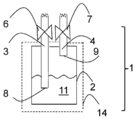
도 1은 Co-함유 막 형성 조성물 전달 장치(1)의 일 구현예의 측단면도이다.
도 2는 Co-함유 막 형성 조성물 전달 장치(1)의 제2 구현예의 측단면도이다.
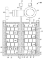
도 3은 고체 Co-함유 막 형성 조성물을 승화시키기 위한 고체 전구체 승화기(100)의 예시적 구현예의 측단면도이다.
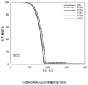
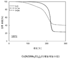
도 4는 Co[N(SiMe3)2]2(THF), Co[N(SiMe2Et)2]2(THF), Co[N(SiMe3)2]2(py), Co[N(SiMe3)2]2(NMe2Et), Co[N(SiMe3)2]2(NMeEt2), Co[N(SiMe3)2]2(NEt3), Co[N(SiMe3)2]2(Me-피롤리딘), 및 Co[N(SiMe2Et)2]2(NMe2Et)의 온도 증가에 따른 중량 손실의 백분율을 나타낸, 1010 mbar 하에서의 비교 개방 컵 열중량 측정 분석(TGA) 그래프이다.
도 5는 Co[N(SiMe2Et)2]2(THF), Co[N(SiMe3)2]2(py), Co[N(SiMe3)2]2(NMeEt2), Co[N(SiMe3)2]2(NEt3), Co[N(SiMe3)2]2(Me-피롤리딘), 및 Co[N(SiMe2Et)2]2(NMe2Et)의 온도 증가에 따른 중량 손실의 백분율을 나타낸, 20 mbar 하에서의 비교 개방 컵 TGA 그래프이다.
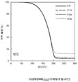
도 6은 안정성 시험 전 및 150℃에서 1주의 안정성 시험 후에, Co[N(SiMe3)2]2(py)의 온도 증가에 따른 중량 손실의 백분율을 나타낸 TGA 그래프이다.
도 7은 안정성 시험 전 및 90℃에서 1주, 2주, 및 3주, 및 1개월 및 2개월의 안정성 시험 후에, Co[N(SiMe3)2]2(NMe2Et)의 온도 증가에 따른 중량 손실의 백분율을 나타낸 TGA 그래프이다.
도 8은 안정성 시험 전 및 80℃에서 1주, 2주, 및 3주의 안정성 시험 후에, Co[N(SiMe3)2]2(NMeEt2)의 온도 증가에 따른 중량 손실의 백분율을 나타낸 TGA 그래프이다.
도 9는 안정성 시험 전 및 110℃에서 1주 및 2주의 안정성 시험 후에, Co[N(SiMe3)2]2(1-Me-피롤리딘)의 온도 증가에 따른 중량 손실의 백분율을 나타낸 TGA 그래프이다.
도 10은 안정성 시험 전 및 120℃에서 1주 및 2주의 안정성 시험 후에, Co[N(SiMe2Et)2]2(NMe2Et)의 온도 증가에 따른 중량 손실의 백분율을 나타낸 TGA 그래프이다.
Claims (15)
- 기판 상에 Co-함유 층을 증착하는 방법으로서, Co-함유 막 형성 조성물의 증기를 그 안에 배치된 기판을 갖는 반응기내로 도입하는 단계로서, Co-함유 막 형성 조성물이 Co[N(SiMe3)2]2(NMe2Et), Co[N(SiMe3)2]2(NMeEt2), 또는 이들의 조합으로부터 선택된 실릴아미드-함유 전구체를 포함하는 단계; 및 증기 증착 방법을 이용하여 Co-함유 층을 형성하기 위해 기판 상에 실릴아미드-함유 전구체의 적어도 일부를 증착시키는 단계를 포함하는 방법.
- 제1항에 있어서, 실릴아미드-함유 전구체가 Co[N(SiMe3)2]2(NMe2Et)인 방법.
- 제1항에 있어서, 실릴아미드-함유 전구체가 Co[N(SiMe3)2]2(NMeEt2)인 방법.
- 제1항 내지 제3항 중 어느 한 항에 있어서, Co-함유 층이 Co인 방법.
- 제1항 내지 제3항 중 어느 한 항에 있어서, Co-함유 층이 CoSi2인 방법.
- 제4항 또는 제5항에 있어서, 기판이 SiO2인 방법.
- 제5항에 있어서, 기판이 Si인 방법.
- 기판 상에 Co-함유 층을 증착하는 방법으로서,
Co-함유 막 형성 조성물을 포함하는 Co-함유 막 형성 조성물 전달 장치를 유동적으로 증기 증착 챔버에 연결시키는 단계로서, Co-함유 막 형성 조성물이 Co[N(SiMe3)2]2(NMe2Et), Co[N(SiMe3)2]2(NMeEt2), 또는 이들의 조합으로부터 선택된 실릴아미드-함유 전구체를 포함하는 단계;
Co-함유 막 형성 조성물의 대략 0.2 Torr(대략 27 Pascal) 내지 대략 1.5 Torr(대략 200 Pascal)의 증기압을 발생시키는 온도까지 Co-함유 막 형성 조성물 전달 장치를 가열하는 단계;
Co-함유 막 형성 조성물의 증기를 그 안에 배치된 기판을 갖는 증기 증착 챔버내로 전달하는 단계; 및
증기 증착 방법을 이용하여 Co-함유 층을 형성하기 위해 기판 상에 실릴아미드-함유 전구체의 적어도 일부를 증착시키는 단계를 포함하는 방법. - 제8항에 있어서, 2주 내지 12개월 범위의 시간 동안 소정 온도에서 Co-함유 막 형성 조성물 전달 장치를 유지하는 것을 추가로 포함하는 방법.
- 제8항 또는 제9항에 있어서, 실릴아미드-함유 전구체가 Co[N(SiMe3)2]2(NMe2Et)인 방법.
- 제1항 내지 제10항 중 어느 한 항의 방법의 생성물을 포함하는, 코발트 니트라이드 막 코팅된 기판.
- Co[N(SiMe3)2]2(NMe2Et), Co[N(SiMe3)2]2(NMeEt2), 또는 이들의 조합으로부터 선택된 실릴아미드-함유 전구체를 포함하고, 열중량 분석에 의해, 80℃에서 2주 후에 5% 미만의 잔류 질량을 나타내는 열 안정성을 갖는, 코발트-함유 막 형성 조성물.
- 제12항에 있어서, 실릴아미드-함유 전구체가 Co[N(SiMe3)2]2(NMe2Et)이고, 열중량 분석에 의해, 90℃에서 2개월 후에 5% 미만의 잔류 질량을 나타내는 열 안정성을 갖는, 코발트-함유 막 형성 조성물.
- 제12항에 있어서, Co-함유 막 형성 조성물이 Co[N(SiMe3)2]2(NMe2Et), Co[N(SiMe3)2]2(NMeEt2), 또는 이들의 조합으로부터 선택된 실릴아미드-함유 전구체로 본질적으로 이루어진, 코발트-함유 막 형성 조성물.
- 제12항에 있어서, Co-함유 막 형성 조성물이 Co[N(SiMe3)2]2(NMe2Et)로 본질적으로 이루어진, 코발트-함유 막 형성 조성물.
Applications Claiming Priority (3)
| Application Number | Priority Date | Filing Date | Title |
|---|---|---|---|
| US14/986,286 US9719167B2 (en) | 2015-12-31 | 2015-12-31 | Cobalt-containing film forming compositions, their synthesis, and use in film deposition |
| US14/986,286 | 2015-12-31 | ||
| PCT/IB2016/001940 WO2017115138A1 (en) | 2015-12-31 | 2016-12-12 | Cobalt-containing film forming compositions, their synthesis, and use in film deposition |
Publications (2)
| Publication Number | Publication Date |
|---|---|
| KR20180098578A true KR20180098578A (ko) | 2018-09-04 |
| KR102653603B1 KR102653603B1 (ko) | 2024-04-01 |
Family
ID=55791519
Family Applications (1)
| Application Number | Title | Priority Date | Filing Date |
|---|---|---|---|
| KR1020187020024A Active KR102653603B1 (ko) | 2015-12-31 | 2016-12-12 | 코발트-함유 막 형성 조성물, 이의 합성, 및 막 증착에서의 용도 |
Country Status (6)
| Country | Link |
|---|---|
| US (1) | US9719167B2 (ko) |
| EP (1) | EP3397790B1 (ko) |
| JP (1) | JP6956086B2 (ko) |
| KR (1) | KR102653603B1 (ko) |
| CN (1) | CN108431295B (ko) |
| WO (1) | WO2017115138A1 (ko) |
Families Citing this family (4)
| Publication number | Priority date | Publication date | Assignee | Title |
|---|---|---|---|---|
| US20180134738A1 (en) | 2016-11-01 | 2018-05-17 | Versum Materials Us, Llc | Disubstituted alkyne dicobalt hexacarbonyl compounds, method of making and method of use thereof |
| US10290540B2 (en) | 2016-11-01 | 2019-05-14 | Versum Materials Us, Llc | Disubstituted alkyne dicobalt hexacarbonyl compounds, method of making and method of use thereof |
| US12312678B2 (en) * | 2018-12-19 | 2025-05-27 | Entegris, Inc. | Methods for depositing a tungsten or molybdenum layer in the presence of a reducing co-reactant |
| TWI866480B (zh) * | 2019-01-17 | 2024-12-11 | 荷蘭商Asm Ip 私人控股有限公司 | 藉由循環沈積製程於基板上形成含過渡金屬膜之方法 |
Citations (3)
| Publication number | Priority date | Publication date | Assignee | Title |
|---|---|---|---|---|
| US6984591B1 (en) * | 2000-04-20 | 2006-01-10 | International Business Machines Corporation | Precursor source mixtures |
| US20140255606A1 (en) * | 2013-03-06 | 2014-09-11 | David Thompson | Methods For Depositing Films Comprising Cobalt And Cobalt Nitrides |
| KR20180098579A (ko) * | 2015-12-31 | 2018-09-04 | 레르 리키드 쏘시에떼 아노님 뿌르 레?드 에렉스뿔라따시옹 데 프로세데 조르즈 클로드 | 망간-함유 막 형성 조성물, 이의 합성, 및 막 증착에서의 용도 |
Family Cites Families (14)
| Publication number | Priority date | Publication date | Assignee | Title |
|---|---|---|---|---|
| US6969539B2 (en) | 2000-09-28 | 2005-11-29 | President And Fellows Of Harvard College | Vapor deposition of metal oxides, silicates and phosphates, and silicon dioxide |
| US6464779B1 (en) * | 2001-01-19 | 2002-10-15 | Novellus Systems, Inc. | Copper atomic layer chemical vapor desposition |
| US9051641B2 (en) | 2001-07-25 | 2015-06-09 | Applied Materials, Inc. | Cobalt deposition on barrier surfaces |
| KR100539278B1 (ko) * | 2003-09-22 | 2005-12-27 | 삼성전자주식회사 | 코발트 실리사이드막 형성 방법 및 반도체 장치의 제조방법. |
| US20060121192A1 (en) | 2004-12-02 | 2006-06-08 | Jurcik Benjamin J | Liquid precursor refill system |
| US20080132050A1 (en) * | 2006-12-05 | 2008-06-05 | Lavoie Adrien R | Deposition process for graded cobalt barrier layers |
| AU2008347088A1 (en) | 2007-04-09 | 2009-07-16 | President And Fellows Of Harvard College | Cobalt nitride layers for copper interconnects and methods for forming them |
| KR20100017171A (ko) * | 2007-05-21 | 2010-02-16 | 레르 리키드 쏘시에떼 아노님 뿌르 레드 에렉스뿔라따시옹 데 프로세데 조르즈 클로드 | 반도체 적용을 위한 신규 코발트 전구체 |
| US20090246952A1 (en) | 2008-03-28 | 2009-10-01 | Tokyo Electron Limited | Method of forming a cobalt metal nitride barrier film |
| KR102193925B1 (ko) * | 2012-09-25 | 2020-12-22 | 엔테그리스, 아이엔씨. | 코발트계 박막의 저온 ald 또는 cvd를 위한 코발트 전구체 |
| US9790247B2 (en) * | 2013-01-31 | 2017-10-17 | L'Air Liquide, Société Anonyme pour l'Etude et l'Exploitation des Procédés Georges Claude | Cobalt-containing compounds, their synthesis, and use in cobalt-containing film deposition |
| US9385033B2 (en) * | 2013-09-27 | 2016-07-05 | Intel Corporation | Method of forming a metal from a cobalt metal precursor |
| US9362228B2 (en) | 2013-10-22 | 2016-06-07 | Globalfoundries Inc. | Electro-migration enhancing method for self-forming barrier process in copper metalization |
| US9601431B2 (en) * | 2014-02-05 | 2017-03-21 | Applied Materials, Inc. | Dielectric/metal barrier integration to prevent copper diffusion |
-
2015
- 2015-12-31 US US14/986,286 patent/US9719167B2/en active Active
-
2016
- 2016-12-12 KR KR1020187020024A patent/KR102653603B1/ko active Active
- 2016-12-12 EP EP16856458.1A patent/EP3397790B1/en active Active
- 2016-12-12 JP JP2018530087A patent/JP6956086B2/ja active Active
- 2016-12-12 WO PCT/IB2016/001940 patent/WO2017115138A1/en not_active Ceased
- 2016-12-12 CN CN201680074877.2A patent/CN108431295B/zh active Active
Patent Citations (3)
| Publication number | Priority date | Publication date | Assignee | Title |
|---|---|---|---|---|
| US6984591B1 (en) * | 2000-04-20 | 2006-01-10 | International Business Machines Corporation | Precursor source mixtures |
| US20140255606A1 (en) * | 2013-03-06 | 2014-09-11 | David Thompson | Methods For Depositing Films Comprising Cobalt And Cobalt Nitrides |
| KR20180098579A (ko) * | 2015-12-31 | 2018-09-04 | 레르 리키드 쏘시에떼 아노님 뿌르 레?드 에렉스뿔라따시옹 데 프로세데 조르즈 클로드 | 망간-함유 막 형성 조성물, 이의 합성, 및 막 증착에서의 용도 |
Also Published As
| Publication number | Publication date |
|---|---|
| WO2017115138A1 (en) | 2017-07-06 |
| JP2019503433A (ja) | 2019-02-07 |
| CN108431295A (zh) | 2018-08-21 |
| CN108431295B (zh) | 2021-01-08 |
| EP3397790B1 (en) | 2023-08-09 |
| KR102653603B1 (ko) | 2024-04-01 |
| JP6956086B2 (ja) | 2021-10-27 |
| EP3397790A1 (en) | 2018-11-07 |
| US20160115588A1 (en) | 2016-04-28 |
| US9719167B2 (en) | 2017-08-01 |
Similar Documents
| Publication | Publication Date | Title |
|---|---|---|
| US11168099B2 (en) | Titanium-containing film forming compositions for vapor deposition of titanium-containing films | |
| US10584039B2 (en) | Titanium-containing film forming compositions for vapor deposition of titanium-containing films | |
| JP7022752B2 (ja) | ジルコニウム、ハフニウム、チタン前駆体およびそれを用いた4族含有膜の堆積 | |
| KR102371411B1 (ko) | 니오븀-함유 필름 형성 조성물 및 니오븀-함유 필름의 기상 증착 | |
| KR20160124028A (ko) | V 족-함유 필름 형성 조성물 및 v 족-함유 필름의 증착 | |
| TW201638098A (zh) | 用於形成含矽及含氧薄膜之氣相沉積方法 | |
| KR102653603B1 (ko) | 코발트-함유 막 형성 조성물, 이의 합성, 및 막 증착에서의 용도 | |
| KR102653070B1 (ko) | 망간-함유 막 형성 조성물, 이의 합성, 및 막 증착에서의 용도 | |
| US20160083405A1 (en) | Tantalum- or vanadium-containing film forming compositions and vapor deposition of tantalum- or vanadium-containing films | |
| JP2020504907A (ja) | ジルコニウム、ハフニウム、チタン前駆体およびそれを用いた4族含有膜の堆積 | |
| JP2020504785A (ja) | ジルコニウム、ハフニウム、チタン前駆体およびそれを用いた4族含有膜の堆積 | |
| US9790591B2 (en) | Titanium-containing film forming compositions for vapor deposition of titanium-containing films | |
| KR102398823B1 (ko) | 4족 전이금속 함유막의 기상 증착을 위한 4족 전이금속 함유막 형성 조성물 | |
| US9738971B2 (en) | Vapor deposition methods to form group 8-containing films |
Legal Events
| Date | Code | Title | Description |
|---|---|---|---|
| PA0105 | International application |
St.27 status event code: A-0-1-A10-A15-nap-PA0105 |
|
| R17-X000 | Change to representative recorded |
St.27 status event code: A-3-3-R10-R17-oth-X000 |
|
| PG1501 | Laying open of application |
St.27 status event code: A-1-1-Q10-Q12-nap-PG1501 |
|
| A201 | Request for examination | ||
| P11-X000 | Amendment of application requested |
St.27 status event code: A-2-2-P10-P11-nap-X000 |
|
| P13-X000 | Application amended |
St.27 status event code: A-2-2-P10-P13-nap-X000 |
|
| PA0201 | Request for examination |
St.27 status event code: A-1-2-D10-D11-exm-PA0201 |
|
| E902 | Notification of reason for refusal | ||
| PE0902 | Notice of grounds for rejection |
St.27 status event code: A-1-2-D10-D21-exm-PE0902 |
|
| E13-X000 | Pre-grant limitation requested |
St.27 status event code: A-2-3-E10-E13-lim-X000 |
|
| P11-X000 | Amendment of application requested |
St.27 status event code: A-2-2-P10-P11-nap-X000 |
|
| P13-X000 | Application amended |
St.27 status event code: A-2-2-P10-P13-nap-X000 |
|
| E701 | Decision to grant or registration of patent right | ||
| PE0701 | Decision of registration |
St.27 status event code: A-1-2-D10-D22-exm-PE0701 |
|
| GRNT | Written decision to grant | ||
| PR0701 | Registration of establishment |
St.27 status event code: A-2-4-F10-F11-exm-PR0701 |
|
| PR1002 | Payment of registration fee |
St.27 status event code: A-2-2-U10-U12-oth-PR1002 Fee payment year number: 1 |
|
| PG1601 | Publication of registration |
St.27 status event code: A-4-4-Q10-Q13-nap-PG1601 |
|
| P22-X000 | Classification modified |
St.27 status event code: A-4-4-P10-P22-nap-X000 |