KR20170130003A - 이방성 도전 필름을 포함하는 표시 장치 및 이방성 도전 필름의 제조 방법 - Google Patents
이방성 도전 필름을 포함하는 표시 장치 및 이방성 도전 필름의 제조 방법 Download PDFInfo
- Publication number
- KR20170130003A KR20170130003A KR1020160060271A KR20160060271A KR20170130003A KR 20170130003 A KR20170130003 A KR 20170130003A KR 1020160060271 A KR1020160060271 A KR 1020160060271A KR 20160060271 A KR20160060271 A KR 20160060271A KR 20170130003 A KR20170130003 A KR 20170130003A
- Authority
- KR
- South Korea
- Prior art keywords
- layer
- conductive particles
- adhesive layer
- region
- support
- Prior art date
Links
Images


Classifications
-
- H—ELECTRICITY
- H10—SEMICONDUCTOR DEVICES; ELECTRIC SOLID-STATE DEVICES NOT OTHERWISE PROVIDED FOR
- H10K—ORGANIC ELECTRIC SOLID-STATE DEVICES
- H10K50/00—Organic light-emitting devices
- H10K50/80—Constructional details
- H10K50/84—Passivation; Containers; Encapsulations
- H10K50/841—Self-supporting sealing arrangements
-
- H—ELECTRICITY
- H01—ELECTRIC ELEMENTS
- H01L—SEMICONDUCTOR DEVICES NOT COVERED BY CLASS H10
- H01L24/00—Arrangements for connecting or disconnecting semiconductor or solid-state bodies; Methods or apparatus related thereto
- H01L24/01—Means for bonding being attached to, or being formed on, the surface to be connected, e.g. chip-to-package, die-attach, "first-level" interconnects; Manufacturing methods related thereto
- H01L24/26—Layer connectors, e.g. plate connectors, solder or adhesive layers; Manufacturing methods related thereto
- H01L24/28—Structure, shape, material or disposition of the layer connectors prior to the connecting process
- H01L24/29—Structure, shape, material or disposition of the layer connectors prior to the connecting process of an individual layer connector
-
- H01L51/524—
-
- G—PHYSICS
- G02—OPTICS
- G02F—OPTICAL DEVICES OR ARRANGEMENTS FOR THE CONTROL OF LIGHT BY MODIFICATION OF THE OPTICAL PROPERTIES OF THE MEDIA OF THE ELEMENTS INVOLVED THEREIN; NON-LINEAR OPTICS; FREQUENCY-CHANGING OF LIGHT; OPTICAL LOGIC ELEMENTS; OPTICAL ANALOGUE/DIGITAL CONVERTERS
- G02F1/00—Devices or arrangements for the control of the intensity, colour, phase, polarisation or direction of light arriving from an independent light source, e.g. switching, gating or modulating; Non-linear optics
- G02F1/01—Devices or arrangements for the control of the intensity, colour, phase, polarisation or direction of light arriving from an independent light source, e.g. switching, gating or modulating; Non-linear optics for the control of the intensity, phase, polarisation or colour
- G02F1/13—Devices or arrangements for the control of the intensity, colour, phase, polarisation or direction of light arriving from an independent light source, e.g. switching, gating or modulating; Non-linear optics for the control of the intensity, phase, polarisation or colour based on liquid crystals, e.g. single liquid crystal display cells
- G02F1/133—Constructional arrangements; Operation of liquid crystal cells; Circuit arrangements
- G02F1/1333—Constructional arrangements; Manufacturing methods
- G02F1/1345—Conductors connecting electrodes to cell terminals
- G02F1/13452—Conductors connecting driver circuitry and terminals of panels
-
- H—ELECTRICITY
- H01—ELECTRIC ELEMENTS
- H01L—SEMICONDUCTOR DEVICES NOT COVERED BY CLASS H10
- H01L24/00—Arrangements for connecting or disconnecting semiconductor or solid-state bodies; Methods or apparatus related thereto
- H01L24/01—Means for bonding being attached to, or being formed on, the surface to be connected, e.g. chip-to-package, die-attach, "first-level" interconnects; Manufacturing methods related thereto
- H01L24/02—Bonding areas ; Manufacturing methods related thereto
- H01L24/04—Structure, shape, material or disposition of the bonding areas prior to the connecting process
- H01L24/05—Structure, shape, material or disposition of the bonding areas prior to the connecting process of an individual bonding area
-
- H—ELECTRICITY
- H01—ELECTRIC ELEMENTS
- H01L—SEMICONDUCTOR DEVICES NOT COVERED BY CLASS H10
- H01L24/00—Arrangements for connecting or disconnecting semiconductor or solid-state bodies; Methods or apparatus related thereto
- H01L24/01—Means for bonding being attached to, or being formed on, the surface to be connected, e.g. chip-to-package, die-attach, "first-level" interconnects; Manufacturing methods related thereto
- H01L24/10—Bump connectors ; Manufacturing methods related thereto
- H01L24/12—Structure, shape, material or disposition of the bump connectors prior to the connecting process
- H01L24/14—Structure, shape, material or disposition of the bump connectors prior to the connecting process of a plurality of bump connectors
-
- H—ELECTRICITY
- H01—ELECTRIC ELEMENTS
- H01L—SEMICONDUCTOR DEVICES NOT COVERED BY CLASS H10
- H01L24/00—Arrangements for connecting or disconnecting semiconductor or solid-state bodies; Methods or apparatus related thereto
- H01L24/01—Means for bonding being attached to, or being formed on, the surface to be connected, e.g. chip-to-package, die-attach, "first-level" interconnects; Manufacturing methods related thereto
- H01L24/26—Layer connectors, e.g. plate connectors, solder or adhesive layers; Manufacturing methods related thereto
- H01L24/27—Manufacturing methods
-
- H—ELECTRICITY
- H01—ELECTRIC ELEMENTS
- H01L—SEMICONDUCTOR DEVICES NOT COVERED BY CLASS H10
- H01L24/00—Arrangements for connecting or disconnecting semiconductor or solid-state bodies; Methods or apparatus related thereto
- H01L24/01—Means for bonding being attached to, or being formed on, the surface to be connected, e.g. chip-to-package, die-attach, "first-level" interconnects; Manufacturing methods related thereto
- H01L24/26—Layer connectors, e.g. plate connectors, solder or adhesive layers; Manufacturing methods related thereto
- H01L24/31—Structure, shape, material or disposition of the layer connectors after the connecting process
- H01L24/32—Structure, shape, material or disposition of the layer connectors after the connecting process of an individual layer connector
-
- H01L27/3276—
-
- H01L51/5243—
-
- H01L51/5246—
-
- H—ELECTRICITY
- H10—SEMICONDUCTOR DEVICES; ELECTRIC SOLID-STATE DEVICES NOT OTHERWISE PROVIDED FOR
- H10K—ORGANIC ELECTRIC SOLID-STATE DEVICES
- H10K50/00—Organic light-emitting devices
- H10K50/80—Constructional details
- H10K50/84—Passivation; Containers; Encapsulations
- H10K50/842—Containers
- H10K50/8423—Metallic sealing arrangements
-
- H—ELECTRICITY
- H10—SEMICONDUCTOR DEVICES; ELECTRIC SOLID-STATE DEVICES NOT OTHERWISE PROVIDED FOR
- H10K—ORGANIC ELECTRIC SOLID-STATE DEVICES
- H10K50/00—Organic light-emitting devices
- H10K50/80—Constructional details
- H10K50/84—Passivation; Containers; Encapsulations
- H10K50/842—Containers
- H10K50/8426—Peripheral sealing arrangements, e.g. adhesives, sealants
-
- H—ELECTRICITY
- H10—SEMICONDUCTOR DEVICES; ELECTRIC SOLID-STATE DEVICES NOT OTHERWISE PROVIDED FOR
- H10K—ORGANIC ELECTRIC SOLID-STATE DEVICES
- H10K59/00—Integrated devices, or assemblies of multiple devices, comprising at least one organic light-emitting element covered by group H10K50/00
- H10K59/10—OLED displays
- H10K59/12—Active-matrix OLED [AMOLED] displays
- H10K59/131—Interconnections, e.g. wiring lines or terminals
-
- H—ELECTRICITY
- H01—ELECTRIC ELEMENTS
- H01L—SEMICONDUCTOR DEVICES NOT COVERED BY CLASS H10
- H01L2224/00—Indexing scheme for arrangements for connecting or disconnecting semiconductor or solid-state bodies and methods related thereto as covered by H01L24/00
- H01L2224/01—Means for bonding being attached to, or being formed on, the surface to be connected, e.g. chip-to-package, die-attach, "first-level" interconnects; Manufacturing methods related thereto
- H01L2224/02—Bonding areas; Manufacturing methods related thereto
- H01L2224/04—Structure, shape, material or disposition of the bonding areas prior to the connecting process
- H01L2224/0401—Bonding areas specifically adapted for bump connectors, e.g. under bump metallisation [UBM]
-
- H—ELECTRICITY
- H01—ELECTRIC ELEMENTS
- H01L—SEMICONDUCTOR DEVICES NOT COVERED BY CLASS H10
- H01L2224/00—Indexing scheme for arrangements for connecting or disconnecting semiconductor or solid-state bodies and methods related thereto as covered by H01L24/00
- H01L2224/01—Means for bonding being attached to, or being formed on, the surface to be connected, e.g. chip-to-package, die-attach, "first-level" interconnects; Manufacturing methods related thereto
- H01L2224/02—Bonding areas; Manufacturing methods related thereto
- H01L2224/04—Structure, shape, material or disposition of the bonding areas prior to the connecting process
- H01L2224/05—Structure, shape, material or disposition of the bonding areas prior to the connecting process of an individual bonding area
- H01L2224/0554—External layer
- H01L2224/05599—Material
- H01L2224/056—Material with a principal constituent of the material being a metal or a metalloid, e.g. boron [B], silicon [Si], germanium [Ge], arsenic [As], antimony [Sb], tellurium [Te] and polonium [Po], and alloys thereof
- H01L2224/05617—Material with a principal constituent of the material being a metal or a metalloid, e.g. boron [B], silicon [Si], germanium [Ge], arsenic [As], antimony [Sb], tellurium [Te] and polonium [Po], and alloys thereof the principal constituent melting at a temperature of greater than or equal to 400°C and less than 950°C
- H01L2224/05624—Aluminium [Al] as principal constituent
-
- H—ELECTRICITY
- H01—ELECTRIC ELEMENTS
- H01L—SEMICONDUCTOR DEVICES NOT COVERED BY CLASS H10
- H01L2224/00—Indexing scheme for arrangements for connecting or disconnecting semiconductor or solid-state bodies and methods related thereto as covered by H01L24/00
- H01L2224/01—Means for bonding being attached to, or being formed on, the surface to be connected, e.g. chip-to-package, die-attach, "first-level" interconnects; Manufacturing methods related thereto
- H01L2224/02—Bonding areas; Manufacturing methods related thereto
- H01L2224/04—Structure, shape, material or disposition of the bonding areas prior to the connecting process
- H01L2224/05—Structure, shape, material or disposition of the bonding areas prior to the connecting process of an individual bonding area
- H01L2224/0554—External layer
- H01L2224/05599—Material
- H01L2224/056—Material with a principal constituent of the material being a metal or a metalloid, e.g. boron [B], silicon [Si], germanium [Ge], arsenic [As], antimony [Sb], tellurium [Te] and polonium [Po], and alloys thereof
- H01L2224/05638—Material with a principal constituent of the material being a metal or a metalloid, e.g. boron [B], silicon [Si], germanium [Ge], arsenic [As], antimony [Sb], tellurium [Te] and polonium [Po], and alloys thereof the principal constituent melting at a temperature of greater than or equal to 950°C and less than 1550°C
- H01L2224/05639—Silver [Ag] as principal constituent
-
- H—ELECTRICITY
- H01—ELECTRIC ELEMENTS
- H01L—SEMICONDUCTOR DEVICES NOT COVERED BY CLASS H10
- H01L2224/00—Indexing scheme for arrangements for connecting or disconnecting semiconductor or solid-state bodies and methods related thereto as covered by H01L24/00
- H01L2224/01—Means for bonding being attached to, or being formed on, the surface to be connected, e.g. chip-to-package, die-attach, "first-level" interconnects; Manufacturing methods related thereto
- H01L2224/02—Bonding areas; Manufacturing methods related thereto
- H01L2224/04—Structure, shape, material or disposition of the bonding areas prior to the connecting process
- H01L2224/05—Structure, shape, material or disposition of the bonding areas prior to the connecting process of an individual bonding area
- H01L2224/0554—External layer
- H01L2224/05599—Material
- H01L2224/056—Material with a principal constituent of the material being a metal or a metalloid, e.g. boron [B], silicon [Si], germanium [Ge], arsenic [As], antimony [Sb], tellurium [Te] and polonium [Po], and alloys thereof
- H01L2224/05638—Material with a principal constituent of the material being a metal or a metalloid, e.g. boron [B], silicon [Si], germanium [Ge], arsenic [As], antimony [Sb], tellurium [Te] and polonium [Po], and alloys thereof the principal constituent melting at a temperature of greater than or equal to 950°C and less than 1550°C
- H01L2224/05644—Gold [Au] as principal constituent
-
- H—ELECTRICITY
- H01—ELECTRIC ELEMENTS
- H01L—SEMICONDUCTOR DEVICES NOT COVERED BY CLASS H10
- H01L2224/00—Indexing scheme for arrangements for connecting or disconnecting semiconductor or solid-state bodies and methods related thereto as covered by H01L24/00
- H01L2224/01—Means for bonding being attached to, or being formed on, the surface to be connected, e.g. chip-to-package, die-attach, "first-level" interconnects; Manufacturing methods related thereto
- H01L2224/02—Bonding areas; Manufacturing methods related thereto
- H01L2224/04—Structure, shape, material or disposition of the bonding areas prior to the connecting process
- H01L2224/05—Structure, shape, material or disposition of the bonding areas prior to the connecting process of an individual bonding area
- H01L2224/0554—External layer
- H01L2224/05599—Material
- H01L2224/056—Material with a principal constituent of the material being a metal or a metalloid, e.g. boron [B], silicon [Si], germanium [Ge], arsenic [As], antimony [Sb], tellurium [Te] and polonium [Po], and alloys thereof
- H01L2224/05638—Material with a principal constituent of the material being a metal or a metalloid, e.g. boron [B], silicon [Si], germanium [Ge], arsenic [As], antimony [Sb], tellurium [Te] and polonium [Po], and alloys thereof the principal constituent melting at a temperature of greater than or equal to 950°C and less than 1550°C
- H01L2224/05647—Copper [Cu] as principal constituent
-
- H—ELECTRICITY
- H01—ELECTRIC ELEMENTS
- H01L—SEMICONDUCTOR DEVICES NOT COVERED BY CLASS H10
- H01L2224/00—Indexing scheme for arrangements for connecting or disconnecting semiconductor or solid-state bodies and methods related thereto as covered by H01L24/00
- H01L2224/01—Means for bonding being attached to, or being formed on, the surface to be connected, e.g. chip-to-package, die-attach, "first-level" interconnects; Manufacturing methods related thereto
- H01L2224/02—Bonding areas; Manufacturing methods related thereto
- H01L2224/04—Structure, shape, material or disposition of the bonding areas prior to the connecting process
- H01L2224/05—Structure, shape, material or disposition of the bonding areas prior to the connecting process of an individual bonding area
- H01L2224/0554—External layer
- H01L2224/05599—Material
- H01L2224/056—Material with a principal constituent of the material being a metal or a metalloid, e.g. boron [B], silicon [Si], germanium [Ge], arsenic [As], antimony [Sb], tellurium [Te] and polonium [Po], and alloys thereof
- H01L2224/05638—Material with a principal constituent of the material being a metal or a metalloid, e.g. boron [B], silicon [Si], germanium [Ge], arsenic [As], antimony [Sb], tellurium [Te] and polonium [Po], and alloys thereof the principal constituent melting at a temperature of greater than or equal to 950°C and less than 1550°C
- H01L2224/05655—Nickel [Ni] as principal constituent
-
- H—ELECTRICITY
- H01—ELECTRIC ELEMENTS
- H01L—SEMICONDUCTOR DEVICES NOT COVERED BY CLASS H10
- H01L2224/00—Indexing scheme for arrangements for connecting or disconnecting semiconductor or solid-state bodies and methods related thereto as covered by H01L24/00
- H01L2224/01—Means for bonding being attached to, or being formed on, the surface to be connected, e.g. chip-to-package, die-attach, "first-level" interconnects; Manufacturing methods related thereto
- H01L2224/02—Bonding areas; Manufacturing methods related thereto
- H01L2224/04—Structure, shape, material or disposition of the bonding areas prior to the connecting process
- H01L2224/05—Structure, shape, material or disposition of the bonding areas prior to the connecting process of an individual bonding area
- H01L2224/0554—External layer
- H01L2224/05599—Material
- H01L2224/056—Material with a principal constituent of the material being a metal or a metalloid, e.g. boron [B], silicon [Si], germanium [Ge], arsenic [As], antimony [Sb], tellurium [Te] and polonium [Po], and alloys thereof
- H01L2224/05663—Material with a principal constituent of the material being a metal or a metalloid, e.g. boron [B], silicon [Si], germanium [Ge], arsenic [As], antimony [Sb], tellurium [Te] and polonium [Po], and alloys thereof the principal constituent melting at a temperature of greater than 1550°C
- H01L2224/05664—Palladium [Pd] as principal constituent
-
- H—ELECTRICITY
- H01—ELECTRIC ELEMENTS
- H01L—SEMICONDUCTOR DEVICES NOT COVERED BY CLASS H10
- H01L2224/00—Indexing scheme for arrangements for connecting or disconnecting semiconductor or solid-state bodies and methods related thereto as covered by H01L24/00
- H01L2224/01—Means for bonding being attached to, or being formed on, the surface to be connected, e.g. chip-to-package, die-attach, "first-level" interconnects; Manufacturing methods related thereto
- H01L2224/02—Bonding areas; Manufacturing methods related thereto
- H01L2224/04—Structure, shape, material or disposition of the bonding areas prior to the connecting process
- H01L2224/05—Structure, shape, material or disposition of the bonding areas prior to the connecting process of an individual bonding area
- H01L2224/0554—External layer
- H01L2224/05599—Material
- H01L2224/056—Material with a principal constituent of the material being a metal or a metalloid, e.g. boron [B], silicon [Si], germanium [Ge], arsenic [As], antimony [Sb], tellurium [Te] and polonium [Po], and alloys thereof
- H01L2224/05663—Material with a principal constituent of the material being a metal or a metalloid, e.g. boron [B], silicon [Si], germanium [Ge], arsenic [As], antimony [Sb], tellurium [Te] and polonium [Po], and alloys thereof the principal constituent melting at a temperature of greater than 1550°C
- H01L2224/05666—Titanium [Ti] as principal constituent
-
- H—ELECTRICITY
- H01—ELECTRIC ELEMENTS
- H01L—SEMICONDUCTOR DEVICES NOT COVERED BY CLASS H10
- H01L2224/00—Indexing scheme for arrangements for connecting or disconnecting semiconductor or solid-state bodies and methods related thereto as covered by H01L24/00
- H01L2224/01—Means for bonding being attached to, or being formed on, the surface to be connected, e.g. chip-to-package, die-attach, "first-level" interconnects; Manufacturing methods related thereto
- H01L2224/02—Bonding areas; Manufacturing methods related thereto
- H01L2224/04—Structure, shape, material or disposition of the bonding areas prior to the connecting process
- H01L2224/05—Structure, shape, material or disposition of the bonding areas prior to the connecting process of an individual bonding area
- H01L2224/0554—External layer
- H01L2224/05599—Material
- H01L2224/056—Material with a principal constituent of the material being a metal or a metalloid, e.g. boron [B], silicon [Si], germanium [Ge], arsenic [As], antimony [Sb], tellurium [Te] and polonium [Po], and alloys thereof
- H01L2224/05663—Material with a principal constituent of the material being a metal or a metalloid, e.g. boron [B], silicon [Si], germanium [Ge], arsenic [As], antimony [Sb], tellurium [Te] and polonium [Po], and alloys thereof the principal constituent melting at a temperature of greater than 1550°C
- H01L2224/05669—Platinum [Pt] as principal constituent
-
- H—ELECTRICITY
- H01—ELECTRIC ELEMENTS
- H01L—SEMICONDUCTOR DEVICES NOT COVERED BY CLASS H10
- H01L2224/00—Indexing scheme for arrangements for connecting or disconnecting semiconductor or solid-state bodies and methods related thereto as covered by H01L24/00
- H01L2224/01—Means for bonding being attached to, or being formed on, the surface to be connected, e.g. chip-to-package, die-attach, "first-level" interconnects; Manufacturing methods related thereto
- H01L2224/02—Bonding areas; Manufacturing methods related thereto
- H01L2224/04—Structure, shape, material or disposition of the bonding areas prior to the connecting process
- H01L2224/05—Structure, shape, material or disposition of the bonding areas prior to the connecting process of an individual bonding area
- H01L2224/0554—External layer
- H01L2224/05599—Material
- H01L2224/056—Material with a principal constituent of the material being a metal or a metalloid, e.g. boron [B], silicon [Si], germanium [Ge], arsenic [As], antimony [Sb], tellurium [Te] and polonium [Po], and alloys thereof
- H01L2224/05663—Material with a principal constituent of the material being a metal or a metalloid, e.g. boron [B], silicon [Si], germanium [Ge], arsenic [As], antimony [Sb], tellurium [Te] and polonium [Po], and alloys thereof the principal constituent melting at a temperature of greater than 1550°C
- H01L2224/05671—Chromium [Cr] as principal constituent
-
- H—ELECTRICITY
- H01—ELECTRIC ELEMENTS
- H01L—SEMICONDUCTOR DEVICES NOT COVERED BY CLASS H10
- H01L2224/00—Indexing scheme for arrangements for connecting or disconnecting semiconductor or solid-state bodies and methods related thereto as covered by H01L24/00
- H01L2224/01—Means for bonding being attached to, or being formed on, the surface to be connected, e.g. chip-to-package, die-attach, "first-level" interconnects; Manufacturing methods related thereto
- H01L2224/02—Bonding areas; Manufacturing methods related thereto
- H01L2224/04—Structure, shape, material or disposition of the bonding areas prior to the connecting process
- H01L2224/05—Structure, shape, material or disposition of the bonding areas prior to the connecting process of an individual bonding area
- H01L2224/0554—External layer
- H01L2224/05599—Material
- H01L2224/056—Material with a principal constituent of the material being a metal or a metalloid, e.g. boron [B], silicon [Si], germanium [Ge], arsenic [As], antimony [Sb], tellurium [Te] and polonium [Po], and alloys thereof
- H01L2224/05663—Material with a principal constituent of the material being a metal or a metalloid, e.g. boron [B], silicon [Si], germanium [Ge], arsenic [As], antimony [Sb], tellurium [Te] and polonium [Po], and alloys thereof the principal constituent melting at a temperature of greater than 1550°C
- H01L2224/0568—Molybdenum [Mo] as principal constituent
-
- H—ELECTRICITY
- H01—ELECTRIC ELEMENTS
- H01L—SEMICONDUCTOR DEVICES NOT COVERED BY CLASS H10
- H01L2224/00—Indexing scheme for arrangements for connecting or disconnecting semiconductor or solid-state bodies and methods related thereto as covered by H01L24/00
- H01L2224/01—Means for bonding being attached to, or being formed on, the surface to be connected, e.g. chip-to-package, die-attach, "first-level" interconnects; Manufacturing methods related thereto
- H01L2224/02—Bonding areas; Manufacturing methods related thereto
- H01L2224/04—Structure, shape, material or disposition of the bonding areas prior to the connecting process
- H01L2224/05—Structure, shape, material or disposition of the bonding areas prior to the connecting process of an individual bonding area
- H01L2224/0554—External layer
- H01L2224/05599—Material
- H01L2224/056—Material with a principal constituent of the material being a metal or a metalloid, e.g. boron [B], silicon [Si], germanium [Ge], arsenic [As], antimony [Sb], tellurium [Te] and polonium [Po], and alloys thereof
- H01L2224/05663—Material with a principal constituent of the material being a metal or a metalloid, e.g. boron [B], silicon [Si], germanium [Ge], arsenic [As], antimony [Sb], tellurium [Te] and polonium [Po], and alloys thereof the principal constituent melting at a temperature of greater than 1550°C
- H01L2224/05681—Tantalum [Ta] as principal constituent
-
- H—ELECTRICITY
- H01—ELECTRIC ELEMENTS
- H01L—SEMICONDUCTOR DEVICES NOT COVERED BY CLASS H10
- H01L2224/00—Indexing scheme for arrangements for connecting or disconnecting semiconductor or solid-state bodies and methods related thereto as covered by H01L24/00
- H01L2224/01—Means for bonding being attached to, or being formed on, the surface to be connected, e.g. chip-to-package, die-attach, "first-level" interconnects; Manufacturing methods related thereto
- H01L2224/02—Bonding areas; Manufacturing methods related thereto
- H01L2224/04—Structure, shape, material or disposition of the bonding areas prior to the connecting process
- H01L2224/05—Structure, shape, material or disposition of the bonding areas prior to the connecting process of an individual bonding area
- H01L2224/0554—External layer
- H01L2224/05599—Material
- H01L2224/056—Material with a principal constituent of the material being a metal or a metalloid, e.g. boron [B], silicon [Si], germanium [Ge], arsenic [As], antimony [Sb], tellurium [Te] and polonium [Po], and alloys thereof
- H01L2224/05663—Material with a principal constituent of the material being a metal or a metalloid, e.g. boron [B], silicon [Si], germanium [Ge], arsenic [As], antimony [Sb], tellurium [Te] and polonium [Po], and alloys thereof the principal constituent melting at a temperature of greater than 1550°C
- H01L2224/05684—Tungsten [W] as principal constituent
-
- H—ELECTRICITY
- H01—ELECTRIC ELEMENTS
- H01L—SEMICONDUCTOR DEVICES NOT COVERED BY CLASS H10
- H01L2224/00—Indexing scheme for arrangements for connecting or disconnecting semiconductor or solid-state bodies and methods related thereto as covered by H01L24/00
- H01L2224/01—Means for bonding being attached to, or being formed on, the surface to be connected, e.g. chip-to-package, die-attach, "first-level" interconnects; Manufacturing methods related thereto
- H01L2224/10—Bump connectors; Manufacturing methods related thereto
- H01L2224/12—Structure, shape, material or disposition of the bump connectors prior to the connecting process
- H01L2224/13—Structure, shape, material or disposition of the bump connectors prior to the connecting process of an individual bump connector
- H01L2224/13001—Core members of the bump connector
- H01L2224/1301—Shape
- H01L2224/13016—Shape in side view
- H01L2224/13017—Shape in side view being non uniform along the bump connector
-
- H—ELECTRICITY
- H01—ELECTRIC ELEMENTS
- H01L—SEMICONDUCTOR DEVICES NOT COVERED BY CLASS H10
- H01L2224/00—Indexing scheme for arrangements for connecting or disconnecting semiconductor or solid-state bodies and methods related thereto as covered by H01L24/00
- H01L2224/01—Means for bonding being attached to, or being formed on, the surface to be connected, e.g. chip-to-package, die-attach, "first-level" interconnects; Manufacturing methods related thereto
- H01L2224/10—Bump connectors; Manufacturing methods related thereto
- H01L2224/15—Structure, shape, material or disposition of the bump connectors after the connecting process
- H01L2224/16—Structure, shape, material or disposition of the bump connectors after the connecting process of an individual bump connector
- H01L2224/161—Disposition
- H01L2224/16151—Disposition the bump connector connecting between a semiconductor or solid-state body and an item not being a semiconductor or solid-state body, e.g. chip-to-substrate, chip-to-passive
- H01L2224/16221—Disposition the bump connector connecting between a semiconductor or solid-state body and an item not being a semiconductor or solid-state body, e.g. chip-to-substrate, chip-to-passive the body and the item being stacked
- H01L2224/16225—Disposition the bump connector connecting between a semiconductor or solid-state body and an item not being a semiconductor or solid-state body, e.g. chip-to-substrate, chip-to-passive the body and the item being stacked the item being non-metallic, e.g. insulating substrate with or without metallisation
- H01L2224/16238—Disposition the bump connector connecting between a semiconductor or solid-state body and an item not being a semiconductor or solid-state body, e.g. chip-to-substrate, chip-to-passive the body and the item being stacked the item being non-metallic, e.g. insulating substrate with or without metallisation the bump connector connecting to a bonding area protruding from the surface of the item
-
- H—ELECTRICITY
- H01—ELECTRIC ELEMENTS
- H01L—SEMICONDUCTOR DEVICES NOT COVERED BY CLASS H10
- H01L2224/00—Indexing scheme for arrangements for connecting or disconnecting semiconductor or solid-state bodies and methods related thereto as covered by H01L24/00
- H01L2224/01—Means for bonding being attached to, or being formed on, the surface to be connected, e.g. chip-to-package, die-attach, "first-level" interconnects; Manufacturing methods related thereto
- H01L2224/26—Layer connectors, e.g. plate connectors, solder or adhesive layers; Manufacturing methods related thereto
- H01L2224/27—Manufacturing methods
- H01L2224/271—Manufacture and pre-treatment of the layer connector preform
-
- H—ELECTRICITY
- H01—ELECTRIC ELEMENTS
- H01L—SEMICONDUCTOR DEVICES NOT COVERED BY CLASS H10
- H01L2224/00—Indexing scheme for arrangements for connecting or disconnecting semiconductor or solid-state bodies and methods related thereto as covered by H01L24/00
- H01L2224/01—Means for bonding being attached to, or being formed on, the surface to be connected, e.g. chip-to-package, die-attach, "first-level" interconnects; Manufacturing methods related thereto
- H01L2224/26—Layer connectors, e.g. plate connectors, solder or adhesive layers; Manufacturing methods related thereto
- H01L2224/27—Manufacturing methods
- H01L2224/276—Manufacturing methods by patterning a pre-deposited material
- H01L2224/27618—Manufacturing methods by patterning a pre-deposited material with selective exposure, development and removal of a photosensitive layer material, e.g. of a photosensitive conductive resin
-
- H—ELECTRICITY
- H01—ELECTRIC ELEMENTS
- H01L—SEMICONDUCTOR DEVICES NOT COVERED BY CLASS H10
- H01L2224/00—Indexing scheme for arrangements for connecting or disconnecting semiconductor or solid-state bodies and methods related thereto as covered by H01L24/00
- H01L2224/01—Means for bonding being attached to, or being formed on, the surface to be connected, e.g. chip-to-package, die-attach, "first-level" interconnects; Manufacturing methods related thereto
- H01L2224/26—Layer connectors, e.g. plate connectors, solder or adhesive layers; Manufacturing methods related thereto
- H01L2224/28—Structure, shape, material or disposition of the layer connectors prior to the connecting process
- H01L2224/29—Structure, shape, material or disposition of the layer connectors prior to the connecting process of an individual layer connector
- H01L2224/29001—Core members of the layer connector
- H01L2224/2902—Disposition
- H01L2224/29026—Disposition relative to the bonding area, e.g. bond pad, of the semiconductor or solid-state body
- H01L2224/29028—Disposition relative to the bonding area, e.g. bond pad, of the semiconductor or solid-state body the layer connector being disposed on at least two separate bonding areas, e.g. bond pads
-
- H—ELECTRICITY
- H01—ELECTRIC ELEMENTS
- H01L—SEMICONDUCTOR DEVICES NOT COVERED BY CLASS H10
- H01L2224/00—Indexing scheme for arrangements for connecting or disconnecting semiconductor or solid-state bodies and methods related thereto as covered by H01L24/00
- H01L2224/01—Means for bonding being attached to, or being formed on, the surface to be connected, e.g. chip-to-package, die-attach, "first-level" interconnects; Manufacturing methods related thereto
- H01L2224/26—Layer connectors, e.g. plate connectors, solder or adhesive layers; Manufacturing methods related thereto
- H01L2224/28—Structure, shape, material or disposition of the layer connectors prior to the connecting process
- H01L2224/29—Structure, shape, material or disposition of the layer connectors prior to the connecting process of an individual layer connector
- H01L2224/29001—Core members of the layer connector
- H01L2224/29075—Plural core members
- H01L2224/2908—Plural core members being stacked
- H01L2224/29082—Two-layer arrangements
-
- H—ELECTRICITY
- H01—ELECTRIC ELEMENTS
- H01L—SEMICONDUCTOR DEVICES NOT COVERED BY CLASS H10
- H01L2224/00—Indexing scheme for arrangements for connecting or disconnecting semiconductor or solid-state bodies and methods related thereto as covered by H01L24/00
- H01L2224/01—Means for bonding being attached to, or being formed on, the surface to be connected, e.g. chip-to-package, die-attach, "first-level" interconnects; Manufacturing methods related thereto
- H01L2224/26—Layer connectors, e.g. plate connectors, solder or adhesive layers; Manufacturing methods related thereto
- H01L2224/28—Structure, shape, material or disposition of the layer connectors prior to the connecting process
- H01L2224/29—Structure, shape, material or disposition of the layer connectors prior to the connecting process of an individual layer connector
- H01L2224/29001—Core members of the layer connector
- H01L2224/29075—Plural core members
- H01L2224/2908—Plural core members being stacked
- H01L2224/29083—Three-layer arrangements
-
- H—ELECTRICITY
- H01—ELECTRIC ELEMENTS
- H01L—SEMICONDUCTOR DEVICES NOT COVERED BY CLASS H10
- H01L2224/00—Indexing scheme for arrangements for connecting or disconnecting semiconductor or solid-state bodies and methods related thereto as covered by H01L24/00
- H01L2224/01—Means for bonding being attached to, or being formed on, the surface to be connected, e.g. chip-to-package, die-attach, "first-level" interconnects; Manufacturing methods related thereto
- H01L2224/26—Layer connectors, e.g. plate connectors, solder or adhesive layers; Manufacturing methods related thereto
- H01L2224/28—Structure, shape, material or disposition of the layer connectors prior to the connecting process
- H01L2224/29—Structure, shape, material or disposition of the layer connectors prior to the connecting process of an individual layer connector
- H01L2224/29001—Core members of the layer connector
- H01L2224/29099—Material
- H01L2224/2919—Material with a principal constituent of the material being a polymer, e.g. polyester, phenolic based polymer, epoxy
-
- H—ELECTRICITY
- H01—ELECTRIC ELEMENTS
- H01L—SEMICONDUCTOR DEVICES NOT COVERED BY CLASS H10
- H01L2224/00—Indexing scheme for arrangements for connecting or disconnecting semiconductor or solid-state bodies and methods related thereto as covered by H01L24/00
- H01L2224/01—Means for bonding being attached to, or being formed on, the surface to be connected, e.g. chip-to-package, die-attach, "first-level" interconnects; Manufacturing methods related thereto
- H01L2224/26—Layer connectors, e.g. plate connectors, solder or adhesive layers; Manufacturing methods related thereto
- H01L2224/28—Structure, shape, material or disposition of the layer connectors prior to the connecting process
- H01L2224/29—Structure, shape, material or disposition of the layer connectors prior to the connecting process of an individual layer connector
- H01L2224/29001—Core members of the layer connector
- H01L2224/29099—Material
- H01L2224/29198—Material with a principal constituent of the material being a combination of two or more materials in the form of a matrix with a filler, i.e. being a hybrid material, e.g. segmented structures, foams
- H01L2224/29199—Material of the matrix
- H01L2224/2929—Material of the matrix with a principal constituent of the material being a polymer, e.g. polyester, phenolic based polymer, epoxy
-
- H—ELECTRICITY
- H01—ELECTRIC ELEMENTS
- H01L—SEMICONDUCTOR DEVICES NOT COVERED BY CLASS H10
- H01L2224/00—Indexing scheme for arrangements for connecting or disconnecting semiconductor or solid-state bodies and methods related thereto as covered by H01L24/00
- H01L2224/01—Means for bonding being attached to, or being formed on, the surface to be connected, e.g. chip-to-package, die-attach, "first-level" interconnects; Manufacturing methods related thereto
- H01L2224/26—Layer connectors, e.g. plate connectors, solder or adhesive layers; Manufacturing methods related thereto
- H01L2224/28—Structure, shape, material or disposition of the layer connectors prior to the connecting process
- H01L2224/29—Structure, shape, material or disposition of the layer connectors prior to the connecting process of an individual layer connector
- H01L2224/29001—Core members of the layer connector
- H01L2224/29099—Material
- H01L2224/29198—Material with a principal constituent of the material being a combination of two or more materials in the form of a matrix with a filler, i.e. being a hybrid material, e.g. segmented structures, foams
- H01L2224/29298—Fillers
- H01L2224/29299—Base material
- H01L2224/2939—Base material with a principal constituent of the material being a polymer, e.g. polyester, phenolic based polymer, epoxy
-
- H—ELECTRICITY
- H01—ELECTRIC ELEMENTS
- H01L—SEMICONDUCTOR DEVICES NOT COVERED BY CLASS H10
- H01L2224/00—Indexing scheme for arrangements for connecting or disconnecting semiconductor or solid-state bodies and methods related thereto as covered by H01L24/00
- H01L2224/01—Means for bonding being attached to, or being formed on, the surface to be connected, e.g. chip-to-package, die-attach, "first-level" interconnects; Manufacturing methods related thereto
- H01L2224/26—Layer connectors, e.g. plate connectors, solder or adhesive layers; Manufacturing methods related thereto
- H01L2224/28—Structure, shape, material or disposition of the layer connectors prior to the connecting process
- H01L2224/29—Structure, shape, material or disposition of the layer connectors prior to the connecting process of an individual layer connector
- H01L2224/29001—Core members of the layer connector
- H01L2224/29099—Material
- H01L2224/29198—Material with a principal constituent of the material being a combination of two or more materials in the form of a matrix with a filler, i.e. being a hybrid material, e.g. segmented structures, foams
- H01L2224/29298—Fillers
- H01L2224/29399—Coating material
- H01L2224/294—Coating material with a principal constituent of the material being a metal or a metalloid, e.g. boron [B], silicon [Si], germanium [Ge], arsenic [As], antimony [Sb], tellurium [Te] and polonium [Po], and alloys thereof
- H01L2224/29438—Coating material with a principal constituent of the material being a metal or a metalloid, e.g. boron [B], silicon [Si], germanium [Ge], arsenic [As], antimony [Sb], tellurium [Te] and polonium [Po], and alloys thereof the principal constituent melting at a temperature of greater than or equal to 950°C and less than 1550°C
- H01L2224/29439—Silver [Ag] as principal constituent
-
- H—ELECTRICITY
- H01—ELECTRIC ELEMENTS
- H01L—SEMICONDUCTOR DEVICES NOT COVERED BY CLASS H10
- H01L2224/00—Indexing scheme for arrangements for connecting or disconnecting semiconductor or solid-state bodies and methods related thereto as covered by H01L24/00
- H01L2224/01—Means for bonding being attached to, or being formed on, the surface to be connected, e.g. chip-to-package, die-attach, "first-level" interconnects; Manufacturing methods related thereto
- H01L2224/26—Layer connectors, e.g. plate connectors, solder or adhesive layers; Manufacturing methods related thereto
- H01L2224/28—Structure, shape, material or disposition of the layer connectors prior to the connecting process
- H01L2224/29—Structure, shape, material or disposition of the layer connectors prior to the connecting process of an individual layer connector
- H01L2224/29001—Core members of the layer connector
- H01L2224/29099—Material
- H01L2224/29198—Material with a principal constituent of the material being a combination of two or more materials in the form of a matrix with a filler, i.e. being a hybrid material, e.g. segmented structures, foams
- H01L2224/29298—Fillers
- H01L2224/29399—Coating material
- H01L2224/294—Coating material with a principal constituent of the material being a metal or a metalloid, e.g. boron [B], silicon [Si], germanium [Ge], arsenic [As], antimony [Sb], tellurium [Te] and polonium [Po], and alloys thereof
- H01L2224/29438—Coating material with a principal constituent of the material being a metal or a metalloid, e.g. boron [B], silicon [Si], germanium [Ge], arsenic [As], antimony [Sb], tellurium [Te] and polonium [Po], and alloys thereof the principal constituent melting at a temperature of greater than or equal to 950°C and less than 1550°C
- H01L2224/29444—Gold [Au] as principal constituent
-
- H—ELECTRICITY
- H01—ELECTRIC ELEMENTS
- H01L—SEMICONDUCTOR DEVICES NOT COVERED BY CLASS H10
- H01L2224/00—Indexing scheme for arrangements for connecting or disconnecting semiconductor or solid-state bodies and methods related thereto as covered by H01L24/00
- H01L2224/01—Means for bonding being attached to, or being formed on, the surface to be connected, e.g. chip-to-package, die-attach, "first-level" interconnects; Manufacturing methods related thereto
- H01L2224/26—Layer connectors, e.g. plate connectors, solder or adhesive layers; Manufacturing methods related thereto
- H01L2224/28—Structure, shape, material or disposition of the layer connectors prior to the connecting process
- H01L2224/29—Structure, shape, material or disposition of the layer connectors prior to the connecting process of an individual layer connector
- H01L2224/29001—Core members of the layer connector
- H01L2224/29099—Material
- H01L2224/29198—Material with a principal constituent of the material being a combination of two or more materials in the form of a matrix with a filler, i.e. being a hybrid material, e.g. segmented structures, foams
- H01L2224/29298—Fillers
- H01L2224/29399—Coating material
- H01L2224/294—Coating material with a principal constituent of the material being a metal or a metalloid, e.g. boron [B], silicon [Si], germanium [Ge], arsenic [As], antimony [Sb], tellurium [Te] and polonium [Po], and alloys thereof
- H01L2224/29438—Coating material with a principal constituent of the material being a metal or a metalloid, e.g. boron [B], silicon [Si], germanium [Ge], arsenic [As], antimony [Sb], tellurium [Te] and polonium [Po], and alloys thereof the principal constituent melting at a temperature of greater than or equal to 950°C and less than 1550°C
- H01L2224/29447—Copper [Cu] as principal constituent
-
- H—ELECTRICITY
- H01—ELECTRIC ELEMENTS
- H01L—SEMICONDUCTOR DEVICES NOT COVERED BY CLASS H10
- H01L2224/00—Indexing scheme for arrangements for connecting or disconnecting semiconductor or solid-state bodies and methods related thereto as covered by H01L24/00
- H01L2224/01—Means for bonding being attached to, or being formed on, the surface to be connected, e.g. chip-to-package, die-attach, "first-level" interconnects; Manufacturing methods related thereto
- H01L2224/26—Layer connectors, e.g. plate connectors, solder or adhesive layers; Manufacturing methods related thereto
- H01L2224/28—Structure, shape, material or disposition of the layer connectors prior to the connecting process
- H01L2224/29—Structure, shape, material or disposition of the layer connectors prior to the connecting process of an individual layer connector
- H01L2224/29001—Core members of the layer connector
- H01L2224/29099—Material
- H01L2224/29198—Material with a principal constituent of the material being a combination of two or more materials in the form of a matrix with a filler, i.e. being a hybrid material, e.g. segmented structures, foams
- H01L2224/29298—Fillers
- H01L2224/29399—Coating material
- H01L2224/294—Coating material with a principal constituent of the material being a metal or a metalloid, e.g. boron [B], silicon [Si], germanium [Ge], arsenic [As], antimony [Sb], tellurium [Te] and polonium [Po], and alloys thereof
- H01L2224/29438—Coating material with a principal constituent of the material being a metal or a metalloid, e.g. boron [B], silicon [Si], germanium [Ge], arsenic [As], antimony [Sb], tellurium [Te] and polonium [Po], and alloys thereof the principal constituent melting at a temperature of greater than or equal to 950°C and less than 1550°C
- H01L2224/29455—Nickel [Ni] as principal constituent
-
- H—ELECTRICITY
- H01—ELECTRIC ELEMENTS
- H01L—SEMICONDUCTOR DEVICES NOT COVERED BY CLASS H10
- H01L2224/00—Indexing scheme for arrangements for connecting or disconnecting semiconductor or solid-state bodies and methods related thereto as covered by H01L24/00
- H01L2224/01—Means for bonding being attached to, or being formed on, the surface to be connected, e.g. chip-to-package, die-attach, "first-level" interconnects; Manufacturing methods related thereto
- H01L2224/26—Layer connectors, e.g. plate connectors, solder or adhesive layers; Manufacturing methods related thereto
- H01L2224/28—Structure, shape, material or disposition of the layer connectors prior to the connecting process
- H01L2224/29—Structure, shape, material or disposition of the layer connectors prior to the connecting process of an individual layer connector
- H01L2224/29001—Core members of the layer connector
- H01L2224/29099—Material
- H01L2224/29198—Material with a principal constituent of the material being a combination of two or more materials in the form of a matrix with a filler, i.e. being a hybrid material, e.g. segmented structures, foams
- H01L2224/29298—Fillers
- H01L2224/29399—Coating material
- H01L2224/294—Coating material with a principal constituent of the material being a metal or a metalloid, e.g. boron [B], silicon [Si], germanium [Ge], arsenic [As], antimony [Sb], tellurium [Te] and polonium [Po], and alloys thereof
- H01L2224/29438—Coating material with a principal constituent of the material being a metal or a metalloid, e.g. boron [B], silicon [Si], germanium [Ge], arsenic [As], antimony [Sb], tellurium [Te] and polonium [Po], and alloys thereof the principal constituent melting at a temperature of greater than or equal to 950°C and less than 1550°C
- H01L2224/29457—Cobalt [Co] as principal constituent
-
- H—ELECTRICITY
- H01—ELECTRIC ELEMENTS
- H01L—SEMICONDUCTOR DEVICES NOT COVERED BY CLASS H10
- H01L2224/00—Indexing scheme for arrangements for connecting or disconnecting semiconductor or solid-state bodies and methods related thereto as covered by H01L24/00
- H01L2224/01—Means for bonding being attached to, or being formed on, the surface to be connected, e.g. chip-to-package, die-attach, "first-level" interconnects; Manufacturing methods related thereto
- H01L2224/26—Layer connectors, e.g. plate connectors, solder or adhesive layers; Manufacturing methods related thereto
- H01L2224/28—Structure, shape, material or disposition of the layer connectors prior to the connecting process
- H01L2224/29—Structure, shape, material or disposition of the layer connectors prior to the connecting process of an individual layer connector
- H01L2224/29001—Core members of the layer connector
- H01L2224/29099—Material
- H01L2224/29198—Material with a principal constituent of the material being a combination of two or more materials in the form of a matrix with a filler, i.e. being a hybrid material, e.g. segmented structures, foams
- H01L2224/29298—Fillers
- H01L2224/29499—Shape or distribution of the fillers
-
- H—ELECTRICITY
- H01—ELECTRIC ELEMENTS
- H01L—SEMICONDUCTOR DEVICES NOT COVERED BY CLASS H10
- H01L2224/00—Indexing scheme for arrangements for connecting or disconnecting semiconductor or solid-state bodies and methods related thereto as covered by H01L24/00
- H01L2224/01—Means for bonding being attached to, or being formed on, the surface to be connected, e.g. chip-to-package, die-attach, "first-level" interconnects; Manufacturing methods related thereto
- H01L2224/26—Layer connectors, e.g. plate connectors, solder or adhesive layers; Manufacturing methods related thereto
- H01L2224/31—Structure, shape, material or disposition of the layer connectors after the connecting process
- H01L2224/32—Structure, shape, material or disposition of the layer connectors after the connecting process of an individual layer connector
- H01L2224/321—Disposition
- H01L2224/32151—Disposition the layer connector connecting between a semiconductor or solid-state body and an item not being a semiconductor or solid-state body, e.g. chip-to-substrate, chip-to-passive
- H01L2224/32221—Disposition the layer connector connecting between a semiconductor or solid-state body and an item not being a semiconductor or solid-state body, e.g. chip-to-substrate, chip-to-passive the body and the item being stacked
- H01L2224/32225—Disposition the layer connector connecting between a semiconductor or solid-state body and an item not being a semiconductor or solid-state body, e.g. chip-to-substrate, chip-to-passive the body and the item being stacked the item being non-metallic, e.g. insulating substrate with or without metallisation
- H01L2224/32227—Disposition the layer connector connecting between a semiconductor or solid-state body and an item not being a semiconductor or solid-state body, e.g. chip-to-substrate, chip-to-passive the body and the item being stacked the item being non-metallic, e.g. insulating substrate with or without metallisation the layer connector connecting to a bond pad of the item
-
- H—ELECTRICITY
- H01—ELECTRIC ELEMENTS
- H01L—SEMICONDUCTOR DEVICES NOT COVERED BY CLASS H10
- H01L2224/00—Indexing scheme for arrangements for connecting or disconnecting semiconductor or solid-state bodies and methods related thereto as covered by H01L24/00
- H01L2224/80—Methods for connecting semiconductor or other solid state bodies using means for bonding being attached to, or being formed on, the surface to be connected
- H01L2224/83—Methods for connecting semiconductor or other solid state bodies using means for bonding being attached to, or being formed on, the surface to be connected using a layer connector
- H01L2224/831—Methods for connecting semiconductor or other solid state bodies using means for bonding being attached to, or being formed on, the surface to be connected using a layer connector the layer connector being supplied to the parts to be connected in the bonding apparatus
- H01L2224/83101—Methods for connecting semiconductor or other solid state bodies using means for bonding being attached to, or being formed on, the surface to be connected using a layer connector the layer connector being supplied to the parts to be connected in the bonding apparatus as prepeg comprising a layer connector, e.g. provided in an insulating plate member
-
- H—ELECTRICITY
- H01—ELECTRIC ELEMENTS
- H01L—SEMICONDUCTOR DEVICES NOT COVERED BY CLASS H10
- H01L2224/00—Indexing scheme for arrangements for connecting or disconnecting semiconductor or solid-state bodies and methods related thereto as covered by H01L24/00
- H01L2224/80—Methods for connecting semiconductor or other solid state bodies using means for bonding being attached to, or being formed on, the surface to be connected
- H01L2224/83—Methods for connecting semiconductor or other solid state bodies using means for bonding being attached to, or being formed on, the surface to be connected using a layer connector
- H01L2224/832—Applying energy for connecting
- H01L2224/83201—Compression bonding
-
- H—ELECTRICITY
- H01—ELECTRIC ELEMENTS
- H01L—SEMICONDUCTOR DEVICES NOT COVERED BY CLASS H10
- H01L2224/00—Indexing scheme for arrangements for connecting or disconnecting semiconductor or solid-state bodies and methods related thereto as covered by H01L24/00
- H01L2224/80—Methods for connecting semiconductor or other solid state bodies using means for bonding being attached to, or being formed on, the surface to be connected
- H01L2224/83—Methods for connecting semiconductor or other solid state bodies using means for bonding being attached to, or being formed on, the surface to be connected using a layer connector
- H01L2224/838—Bonding techniques
- H01L2224/8385—Bonding techniques using a polymer adhesive, e.g. an adhesive based on silicone, epoxy, polyimide, polyester
- H01L2224/83855—Hardening the adhesive by curing, i.e. thermosetting
- H01L2224/83856—Pre-cured adhesive, i.e. B-stage adhesive
-
- H—ELECTRICITY
- H01—ELECTRIC ELEMENTS
- H01L—SEMICONDUCTOR DEVICES NOT COVERED BY CLASS H10
- H01L2224/00—Indexing scheme for arrangements for connecting or disconnecting semiconductor or solid-state bodies and methods related thereto as covered by H01L24/00
- H01L2224/80—Methods for connecting semiconductor or other solid state bodies using means for bonding being attached to, or being formed on, the surface to be connected
- H01L2224/83—Methods for connecting semiconductor or other solid state bodies using means for bonding being attached to, or being formed on, the surface to be connected using a layer connector
- H01L2224/838—Bonding techniques
- H01L2224/8385—Bonding techniques using a polymer adhesive, e.g. an adhesive based on silicone, epoxy, polyimide, polyester
- H01L2224/83855—Hardening the adhesive by curing, i.e. thermosetting
- H01L2224/83862—Heat curing
-
- H01L2227/32—
-
- H—ELECTRICITY
- H01—ELECTRIC ELEMENTS
- H01L—SEMICONDUCTOR DEVICES NOT COVERED BY CLASS H10
- H01L24/00—Arrangements for connecting or disconnecting semiconductor or solid-state bodies; Methods or apparatus related thereto
- H01L24/80—Methods for connecting semiconductor or other solid state bodies using means for bonding being attached to, or being formed on, the surface to be connected
- H01L24/83—Methods for connecting semiconductor or other solid state bodies using means for bonding being attached to, or being formed on, the surface to be connected using a layer connector
-
- H—ELECTRICITY
- H01—ELECTRIC ELEMENTS
- H01R—ELECTRICALLY-CONDUCTIVE CONNECTIONS; STRUCTURAL ASSOCIATIONS OF A PLURALITY OF MUTUALLY-INSULATED ELECTRICAL CONNECTING ELEMENTS; COUPLING DEVICES; CURRENT COLLECTORS
- H01R12/00—Structural associations of a plurality of mutually-insulated electrical connecting elements, specially adapted for printed circuits, e.g. printed circuit boards [PCB], flat or ribbon cables, or like generally planar structures, e.g. terminal strips, terminal blocks; Coupling devices specially adapted for printed circuits, flat or ribbon cables, or like generally planar structures; Terminals specially adapted for contact with, or insertion into, printed circuits, flat or ribbon cables, or like generally planar structures
- H01R12/70—Coupling devices
- H01R12/7076—Coupling devices for connection between PCB and component, e.g. display
Abstract
본 발명의 일 실시예에 따른 표시 장치는, 상기 패드부 위에 위치하는 이방성 도전 필름, 그리고 상기 이방성 도전 필름을 통해 상기 패드부에 부착되어 있으며, 복수의 범프를 포함하는 접속 부재를 포함한다. 상기 이방성 도전 필름은, 각각의 도전 입자의 일부분이 제1 면과 제2 면으로부터 돌출되어 있는 복수의 도전 입자를 포함하는 지지층, 상기 지지층의 상기 제1 면 및 상기 제1 면으로부터 돌출된 상기 도전 입자들의 부분과 접촉하는 제1 접착층, 그리고 상기 지지층의 상기 제2 면 및 상기 제2 면으로부터 돌출된 상기 도전 입자들의 부분과 접촉하는 제2 접착층을 포함한다. 상기 제1 접착층 및 상기 제2 접착층 중 적어도 하나는 상기 패드들과 상기 범퍼들이 중첩하는 제1 영역과 상기 패드들과 상기 범퍼들이 중첩하지 않는 제2 영역에 모두 위치한다.
Description
본 개시는 이방성 도전 필름을 포함하는 표시 장치 및 이방성 도전 필름의 제조 방법에 관한 것이다.
액정 표시 장치, 유기 발광 표시 장치 같은 표시 장치는 영상을 표시하는 표시 패널을 포함한다. 표시 패널의 동작을 제어하기 위해 표시 패널에는 신호의 입출력을 위한 패드부(pad portion)가 있고, 패드부에는 집적회로 칩이나 연성 인쇄회로기판(FPCB)이 부착된다.
집적회로 칩 또는 연성 인쇄회로기판과 패드부 사이의 전기적 접속과 물리적 결합을 위해, 이방성 도전 필름(ACF)이 사용된다. 이방성 도전 필름은 수지 같은 절연층에 도전 입자들(conductive particles)이 배열되어 있는 필름으로, 필름의 두께 방향으로는 도전성을 띠고 필름의 면 방향으로는 절연성을 띤다.
집적회로 칩 또는 연성 인쇄회로기판을 이방성 도전 필름을 통해 패드부에 부착하는 과정에서 이방성 도전 필름에 압력이 가해진다. 이때 도전 입자들이 수지 내에서 유동하여 필름의 면 방향으로 절연성이 저하되거나 필름의 두께 방향으로 도전성이 저하될 수 있다.
실시예들은 도전 입자들의 유동을 방지할 수 있는 이방성 도전 필름을 포함하는 표시 장치 및 그러한 이방성 도전 필름을 제조하는 방법을 제공하는 것이다.
본 발명의 일 실시예에 따른 표시 장치는, 상기 패드부 위에 위치하는 이방성 도전 필름, 그리고 상기 이방성 도전 필름을 통해 상기 패드부에 부착되어 있으며, 복수의 범프를 포함하는 접속 부재를 포함한다. 상기 이방성 도전 필름은, 각각의 도전 입자의 일부분이 제1 면과 제2 면으로부터 돌출되어 있는 복수의 도전 입자를 포함하는 지지층, 상기 지지층의 상기 제1 면 및 상기 제1 면으로부터 돌출된 상기 도전 입자들의 부분과 접촉하는 제1 접착층, 그리고 상기 지지층의 상기 제2 면 및 상기 제2 면으로부터 돌출된 상기 도전 입자들의 부분과 접촉하는 제2 접착층을 포함한다. 상기 제1 접착층 및 상기 제2 접착층 중 적어도 하나는 상기 패드들과 상기 범퍼들이 중첩하는 제1 영역과 상기 패드들과 상기 범퍼들이 중첩하지 않는 제2 영역에 모두 위치한다.
상기 지지층은 상기 제1 접착층 및 상기 제2 접착층과 상이한 재료로 형성되어 있을 수 있다.
상기 지지층은 폴리이미드, 폴리에틸렌 테레프탈레이트, 나일론 6, 폴리비닐리덴 플로라이드, 폴라카보네이트, 폴리부틸렌 숙시네이트 및 폴리에틸렌으로 이루어진 그룹에서 선택된 적어도 하나의 폴리머를 포함할 수 있다.
상기 지지층의 융점이 상기 제1 접착층의 경화점 및 상기 제2 접착층의 경화점보다 높을 수 있다.
제1 방향으로 인접하는 도전 입자들 사이의 간격이 상기 제1 영역과 상기 제2 영역에서 일정할 수 있다.
상기 제1 방향과 교차하는 제2 방향으로 인접하는 도전 입자들 사이의 간격이 상기 제1 영역과 상기 제2 영역에서 일정할 수 있다.
상기 복수의 도전 입자는 평면도에서 장방형 또는 마름모형으로 배열되어 있을 수 있다.
상기 복수의 도전 입자의 직경이 상기 지지층의 두께보다 클 수 있다.
상기 제1 접착층은 상기 제1 영역에 위치하는 부분의 두께가 상기 제2 영역에 위치하는 부분의 두께보다 작을 수 있다.
상기 제2 접착층은 상기 제1 영역에 위치하는 부분의 두께가 상기 제2 영역에 위치하는 부분의 두께보다 작을 수 있다.
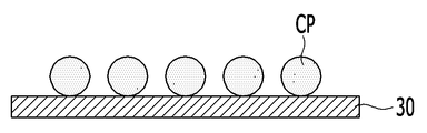
본 발명의 일 실시예에 따른 이방성 도전 필름을 제조하는 방법은, 미경화 수지층에 도전 입자들을 배열하는 단계; 상기 수지층을 경화시켜 상기 도전 입자들을 경화된 수지층 내에 고정하는 단계; 및 상기 경화된 수지층을 식각하여 상기 도전 입자들의 일부분을 노출시키는 지지체를 형성하는 단계를 포함한다.
상기 식각은 상기 지지체의 적어도 한 면에서 상기 도전 입자들의 일부분을 노출시키는 것을 포함할 수 있다.
상기 식각은 반응성 이온 식각을 포함할 수 있다.
상기 지지층은 폴리이미드, 폴리에틸렌 테레프탈레이트, 나일론 6, 폴리비닐리덴 플로라이드, 폴라카보네이트, 폴리부틸렌 숙시네이트 및 폴리에틸렌으로 이루어진 그룹에서 선택된 적어도 하나의 폴리머를 포함할 수 있다.
상기 방법은 상기 지지체의 상기 양면 중 적어도 한 면에 접착층을 형성하는 단계를 더 포함할 수 있다.
상기 접착층은 상기 도전 입자들의 노출된 부분에 접촉하게 형성될 수 있다.
상기 접착층은 상기 지지체 위에 미경화 수지층을 적층하여 형성될 수 있다.
상기 접착층은 상기 지지층과 상이한 재료로 형성될 수 있다.
상기 지지층의 융점이 상기 접착층의 경화점보다 높을 수 있다.
상기 지지층은 각각의 도전 입자의 직경보다 작은 두께로 형성될 수 있다.
실시예들에 따르면, 이방성 도전 필름이 압착되더라도 도전 입자들의 유동이 방지되므로 표시 장치에서 이방성 도전 필름의 두께 방향 도전성과 면 방향 절연성이 향상될 수 있다.
도 1은 본 발명의 일 실시예에 따른 표시 장치를 개략적으로 나타낸 평면도이다.
도 2는 도 1에서 A 영역을 확대하여 나타낸 평면도이다.
도 3은 도 2에서 III-III' 선을 따라 취한 단면의 일 실시예를 나타낸다.
도 4는 도 2에서 III-III' 선을 따라 취한 단면의 일 실시예를 나타낸다.
도 5는 도 2에서 III-III' 선을 따라 취한 단면의 일 실시예를 나타낸다.
도 6은 도 1에서 A 영역의 단면의 일 실시예를 나타낸다.
도 7은 도 1에서 화소 영역의 단면의 일 실시예를 나타낸다.
도 8은 도 1에서 A 영역의 단면의 일 실시예를 나타낸다.
도 9는 도 1에서 화소 영역의 단면의 일 실시예를 나타낸다.
도 10은 본 발명의 일 실시예에 따른 이방성 도전 필름의 단면도이다.
도 11 내지 도 14는 도 10에 도시된 이방성 도전 필름을 제조하는 방법을 나타내는 공정 단면도이다.
도 15는 본 발명의 일 실시예에 따른 이방성 도전 필름의 단면도이다.
도 16은 본 발명의 일 실시예에 따른 이방성 도전 필름의 단면도이다.
도 17 및 도 18은 각각 본 발명의 일 실시예에 따른 도전 입자들의 배치를 나타낸 평면도이다.
이하, 첨부한 도면을 참고로 하여 본 발명의 여러 실시예들에 대하여 본 발명이 속하는 기술 분야에서 통상의 지식을 가진 자가 용이하게 실시할 수 있도록 상세히 설명한다. 본 발명은 여러 가지 상이한 형태로 구현될 수 있으며 여기에서 설명하는 실시예들에 한정되지 않는다.
본 발명을 명확하게 설명하기 위해서 설명과 관계없는 부분은 생략하였으며, 명세서 전체를 통하여 동일 또는 유사한 구성요소에 대해서는 동일한 참조 부호를 붙이도록 한다.
도면에서 나타난 각 구성의 크기 및 두께는 설명의 편의를 위해 임의로 나타내었으므로, 본 발명이 반드시 도시된 바에 한정되지 않는다. 도면에서 여러 층 및 영역을 명확하게 표현하기 위하여 두께를 확대하여 나타내었다. 그리고 도면에서, 설명의 편의를 위해, 일부 층 및 영역의 두께를 과장되게 나타내었다.
층, 막, 영역, 판 등의 부분이 다른 부분 "위에" 또는 "상에" 있다고 할 때, 이는 다른 부분 "바로 위에" 있는 경우뿐 아니라 그 중간에 또 다른 부분이 있는 경우도 포함한다. 반대로 어떤 부분이 다른 부분 "바로 위에" 있다고 할 때에는 중간에 다른 부분이 없는 것을 뜻한다. 또한, 기준이 되는 부분 "위에" 또는 "상에" 있다고 하는 것은 기준이 되는 부분의 위 또는 아래에 위치하는 것이고, 반드시 중력 반대 방향 쪽으로 "위에" 또는 "상에" 위치하는 것을 의미하는 것은 아니다.
명세서 전체에서, 어떤 부분이 어떤 구성요소를 "포함" 한다고 할 때, 이는 특별히 반대되는 기재가 없는 한 다른 구성요소를 제외하는 것이 아니라 다른 구성요소를 더 포함할 수 있는 것을 의미한다.
명세서 전체에서, "평면상"이라 할 때, 이는 대상 부분을 위에서 보았을 때를 의미하며, "단면상"이라 할 때, 이는 대상 부분을 수직으로 자른 단면을 옆에서 보았을 때를 의미한다.
본 발명의 실시예에 따른 표시 장치에 대하여 도면을 참고로 하여 상세하게 설명한다. 표시 장치를 예로 들어 설명할지라도, 본 발명은 이방성 도전 필름을 이용하는 모든 전자 장치에 적용될 수 있다.
도 1은 본 발명의 일 실시예에 따른 표시 장치를 개략적으로 나타낸 평면도이다.
도 1을 참고하면, 본 발명의 일 실시예에 따른 표시 장치는 표시 패널(10) 및 표시 패널(10)에 연결되어 있는 연성 인쇄회로기판(50)을 포함한다.
표시 패널(10)은 영상을 표시하는 표시 영역(display area, DA), 그리고 표시 영역(DA)에 인가되는 각종 신호들을 생성 및/또는 전달하기 위한 소자들 및/또는 배선들이 배치되어 있는, 표시 영역(DA) 외곽의 비표시 영역(non-display area, NDA)을 포함한다. 도 1에서 표시 패널(10)의 하측 영멱만이 비표시 영역(NDA)으로 도시되어 있으나, 표시 패널(10)의 좌우측 가장자리 및/또는 상측 가장자리도 비표시 영역(NDA)에 해당할 수 있다.
표시 패널(10)의 표시 영역(DA)에는 복수의 화소(PX)가 예컨대 행렬 방향으로 배치되어 있다. 표시 영역(DA)에는 복수의 게이트선(도시되지 않음), 복수의 데이터선(도시되지 않음) 같은 신호선들이 또한 배치되어 있다. 복수의 게이트선은 주로 제1 방향(D1)(예컨대, 행 방향)으로 뻗어 있을 수 있고, 복수의 데이터선은 제1 방향(D1)과 교차하는 제2 방향(D2)(예컨대, 열 방향)으로 뻗어 있을 수 있다. 각각의 화소(PX)에는 게이트선과 데이터선이 연결되어, 이들 신호선으로부터 게이트 신호와 데이터 신호를 인가받을 수 있다. 유기 발광 표시 장치의 경우, 표시 영역(DA)에는 예컨대 제2 방향(D2)으로 뻗어 있으며 구동 전압을 화소(PX)에 전달하는 복수의 구동 전압선(도시되지 않음)이 배치되어 있을 수 있다.
표시 패널(10)의 비표시 영역(NDA)에는 표시 패널(10)의 외부로부터 신호를 전달받기 위한 제1 패드부(PP1)가 위치한다. 제1 패드부(PP1)에는 연성 인쇄회로기판(50)의 일단이 연결되어 있다. 제1 패드부(PP1)와 연성 인쇄회로기판(50) 사이에는 이방성 도전 필름 (도시되지 않음)이 위치한다. 연성 인쇄회로기판(50)은 타단이 예컨대 외부의 인쇄회로기판에 연결되어 영상 데이터 같은 신호를 전달할 수 있다.
표시 패널(10)을 구동하기 위한 각종 신호들을 생성 및/또는 처리하는 구동 장치는 표시 패널(10)의 비표시 영역(NDA)이나 연성 인쇄회로기판(50)에 위치할 수 있고, 외부의 인쇄회로기판에 위치할 수도 있다. 구동 장치는 데이터선에 데이터 신호를 인가하는 데이터 구동부, 게이트선에 게이트 신호를 인가하는 게이트 구동부, 그리고 데이터 구동부 및 게이트 구동부를 제어하는 신호 제어부를 포함할 수 있다.
도시된 실시예에서, 데이터 구동부는 집적회로 칩(400) 형태로 표시 영역(DA)과 제1 패드부(PP1) 사이에 위치하는 제2 패드부(PP2)에 실장되어 있다. 제2 패드부(PP2)와 집적회로 칩(400) 사이에는 이방성 도전 필름(도시되지 않음)이 위치한다. 도시된 것과 달리, 데이터 구동부는 연성 인쇄회로기판(50)에 집적회로 칩 형태로 실장되어 테이프 캐리어 패키지(tape carrier package) 형태로 제1 패드부(PP1)에 연결될 수 있다. 게이트 구동부는 집적회로 칩 형태로 제공되거나 표시 패널(10)의 좌/우측 가장자리의 비표시 영역(도시되지 않음)에 집적되어 있을 수 있다. 신호 제어부는 데이터 구동부와 같은 집적회로 칩(400)으로 형성되거나 별개의 집적회로 칩으로 제공될 수 있다.
지금까지 표시 장치의 전체적인 구성에 대해 살펴보았다. 이제, 연성 인쇄회로기판(50)이 제1 패드부(PP1)에 연결되어 있는 부분을 중심으로 본 발명의 일 실시예에 따른 표시 장치에 대해 상세하게 설명한다.
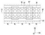
도 2는 도 1에서 A 영역의 확대하여 나타낸 평면도이고, 도 3 내지 도 5는 각각 도 2에서 III-III' 선을 따라 취한 단면의 몇몇 실시예를 나타낸다.
도 2 및 도 3을 참고하면, 연성 인쇄회로기판(50)이 제1 패드부(PP1)에 이방성 도전 필름(20)을 통해 부착되어 있는 상태가 도시된다. 이방성 도전 필름(20)은 압착 및 경화되어 있다.
기판(110) 위에 제1 패드부(PP1)의 패드(P)가 위치하고, 연성 인쇄회로기판(50)은 패드(P)를 향하여 돌출되어 있는 범프(B)를 포함한다. 연성 인쇄회로기판(50)의 범프(B)는 이방성 도전 필름(20) 내의 도전 입자들(CP)을 통해 제1 패드부(PP1)의 패드(P)와 전기적으로 연결되어 있다. 범프(B)와 패드(P)는 전극으로 불릴 수 있다.
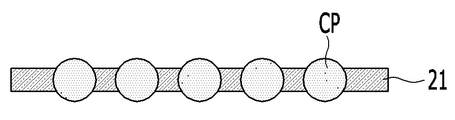
이방성 도전 필름(20)은 3개의 층 즉, 지지층(21), 그리고 지지층(21)의 위와 아래에 각각 위치하는 제1 접착층(22)과 제2 접착층(23)을 포함한다. 지지층(21)은 도전 입자들(CP)을 포함하여 연성 인쇄회로기판(50)을 제1 패드부(PP1)에 전기적으로 연결하는 역할을 하고, 제1 및 제2 접착층(22, 23)은 연성 인쇄회로기판(50)을 제1 패드부(PP1)에 물리적으로 연결하는 역할을 한다.
지지층(21) 내에는 도전 입자들(CP)이 소정 간격으로 단층으로 배열되어 있으며, 표시 장치에 적용하기 전에 이미 경화되어 있는 지지층(21)에 의해 견고하게 그 위치가 고정되어 있다. 인접하는 도전 입자들(CP)은 지지층(21)에 의해 서로 절연된다.
도전 입자들(CP)은 범프(B)와 패드(P)가 서로 마주하며 중첩하고 있는 제1 영역(R1)에 위치하고, 범프(B)와 패드(P)가 중첩하지 않는 제2 영역(R2)에 또한 위치한다. 제1 영역(R1)에서 도전 입자들(CP)은 그 위와 아래에 있는 범프(B) 및 패드(P)와 접촉하여 이들을 통전시킨다. 이에 의해 연성 인쇄회로기판(50)을 통해 전달되는 신호들은 범프(B), 도전 입자(CP) 및 패드(P)를 거쳐 표시 패널(10)로 전송될 수 있다. 제2 영역(R2)에서 도전 입자들(CP)은 고립되어 있다. 즉, 제2 영역(R2)에서 도전 입자들(CP)은 범프(B) 및 패드(P)와 접촉하지 않고, 인접하는 도전 입자들(CP) 간에도 접촉하고 있지 않다. 따라서 제2 영역(R2)에 도전 입자들(CP)이 있더라도 인접하는 범프들(B)이나 패드들(P) 간에 쇼트가 일어나지 않는다. 제2 영역(R2)에는 도전 입자들(CP)이 위치하지 않을 수도 있다.
도전 입자들(CP)은 구형일 수 있으며, 지지층(21)의 두께보다 큰 직경을 가질 수 있다. 도전 입자들(CP)은 수 마이크로미터의 직경 예컨대, 약 2 내지 약 5 마이크로미터의 직경을 가질 수 있다. 따라서 도전 입자들(CP)은 전체가 지지층(21) 내부에 있지 않고 일부분이 지지층(21) 외부로 나와 있다. 즉, 각각의 도전 입자(CP)는 일부분이 지지층(21)의 상면 위로 돌출되고 일부분이 지지층(21)의 하면 아래로 돌출되어 있다. 도전 입자들(CP)은 구형의 폴리머에 니켈, 코발트, 금, 은, 구리 같은 금속층이 코팅되어 있는 구조를 가질 수 있다. 도전 입자들(CP)은 구형 이외의 입체 형상을 가질 수도 있다.
지지층(21) 내의 도전 입자들(CP)은 어떤 방향으로 인접하는 도전 입자들(CP) 사이의 간격이 실질적으로 일정하게 배열되어 있다. 예컨대, 도전 입자들(CP)은 제1 방향(D1)으로 균등한 간격으로 배열되어 있고, 제1 방향(D1)과 교차하는 제2 방향(D2)으로 균등한 간격으로 배열되어 있다. 이러한 균등한 간격은 제1 영역(R1)과 제2 영역(R2)에 걸쳐 유지되는데, 이방성 도전 필름(AFC)의 압착 시 도전 입자들(CP)이 이미 경화되어 있는 지지층(21) 내에서 유동하지 않게 고정되어 있기 때문이다.
지지층(21)의 상면에는 제1 접착층(22)이 위치하고, 지지층(21)의 하면에는 제2 접착층(23)이 위치한다. 제1 및 제2 접착층(22, 23)은 제1 영역(R1)에서는 얇게 형성되어 있지만, 제2 영역(R2)에서는 두껍게 형성되어 있다.
이방성 도전 필름(20)이 연성 인쇄회로기판(50)을 제1 패드부(PP1)에 부착하는데 사용되기 전에 제1 및 제2 접착층(22, 23)은 미경화 상태이고 이방성 도전 필름(20)의 전체 면에 걸쳐 실질적으로 동일한 두께를 가진다. 연성 인쇄회로기판(50)을 제1 패드부(PP1)에 부착하기 위해 이들 사이에 이방성 도전 필름(20)을 사이에 두고 압착하면, 미경화 상태의 제1 및 제2 접착층(22, 23)은 제1 영역(R1)에 있는 부분이 유동하여 제2 영역(R2)으로 밀려나서, 제1 접착층(22)은 인접하는 범프(B) 사이의 공간을 채우고, 제2 접착층(23)은 인접하는 패드(P) 사이의 공간을 채우게 된다. 이에 따라 제1 영역(R1)에서 도전 입자들(CP)이 범프(B) 및 패드(P)와 접촉하여 범프(B)와 패드(P)가 도통하게 되고, 제2 영역(R2)에서는 제1 및 제2 접착층(22, 23)과 연성 인쇄회로기판(50) 및 제1 패드부(PP1)가 접촉하는 면적이 증가하여 접착력이 증가한다. 하지만, 제1 영역(R1)에 있는 제1 및 제2 접착층(22, 23)이 제2 영역(R2)으로 완전히 밀려나지 않고, 일부는 제1 영역(R1)에 남아 있다. 예컨대, 도 3에 도시된 바와 같이, 제1 접착층(22)은 도전 입자들(CP)이 지지층(21)의 상면으로부터 돌출된 높이에 대응하게 남아 있을 수 있고, 제2 접착층(23)은 도전 입자들(CP)이 지지층(21)의 하면으로부터 돌출된 높이에 대응하게 남아 있을 수 있다.
지지층(21)은 이방성 도전 필름(20)을 표시 장치에 적용하기 전후에 모두 경화된 상태이지만, 제1 및 제2 접착층(22, 23)은 표시 장치에 적용하기 전에는 미경화 상태이고 적용 후에는 경화된 상태이다. 따라서 이방성 도전 필름(20)을 표시 장치에 적용하여 압착하고 제1 및 제2 접착층(22, 23)을 경화시키는 과정에서, 지지층(21)의 구조가 유지되므로 지지층(21) 내에 포함된 도전 입자들(CP)이 유동이 어려워 제 위치를 유지할 수 있다. 따라서 쇼트의 발생이 억제되고 도전 입자들(CP)의 포착률이 향상되어, 절연성과 접속 신뢰성을 향상시킬 수 있다. 또한, 도전 입자들(CP)은, 전술한 바와 같이, 제1 영역(R1)과 제2 영역(R2)에서 일정한 간격으로 배열되어 있을 수 있다.
지지층(21)은 제1 및 제2 접착층(22, 23)과 다른 재료로 형성될 수 있다. 예컨대 제1 및 제2 접착층(22, 23)이 열에 의해 경화되는 재료로 형성되는 경우, 지지층(21)은 제1 및 제2 접착층(22, 23)의 경화점보다 융점이 높은 재료로 형성될 수 있다. 그러면 제1 및 제2 접착층(22, 23)을 경화시키기 위한 온도에서 지지층(21)이 유동하지 않으므로 지지층(21) 내의 도전 입자들(CP)이 원래 위치를 유지할 수 있다. 지지층(21)은 예컨대 폴리이미드(polyimide), 폴리에틸렌 테레프탈레이트(polyethylene terephthalate), 나일론 6(nylon 6), 폴리비닐리덴 플로라이드(polyvinylidene fluoride), 폴라카보네이트(polycarbonate), 폴리부틸렌 숙시네이트(polybutylene succinate) 및 폴리에틸렌(polyethylene) 중 적어도 하나를 포함할 수 있지만 이에 제한되지 않는다.
제1 접착층(22) 및 제2 접착층(23)은 절연성과 접착성이 있는 재료로 형성될 수 있으며, 예컨대 열 경화성 수지나 광 경화성 수지로 형성될 수 있다. 제1 접착층(22) 및 제2 접착층(23)은 에폭시 수지층, 아크릴 수지층, 또는 폴리에스테르 수지층일 있지만, 이에 제한되지 않는다.
도 4를 참고하면, 도 3에 도시된 실시예와 비교하여 도전 입자들(CP)이 지지층(21)으로부터 돌출되는 특징에 있어서 차이가 있다. 도전 입자들(CP)은 지지층(21)의 상면 위로 돌출되어 있지만, 지지층(21)의 하면 아래로는 돌출되지 않거나 거의 돌출되어 있지 않다. 그렇더라도, 도전 입자들(CP)은 적어도 제1 영역(R1)에서는 지지층(21)의 하면에 의해 절연되게 완전히 덮여 있지는 않고 일부분이 노출되어 있다. 따라서 제1 영역(R1)에서 도전 입자들(CP)은 범프(B)와 접촉하고 패드(P)와 또한 접촉하고 있어 이들을 전기적으로 연결한다.
도전 입자들(CP)이 지지층(21)의 하면으로부터 돌출되지 않으므로, 지지층(20)의 하면에 있는 제2 접착층(23)은 이방성 도전 필름(20)의 압착 시 제1 영역(R1)에 있는 부분이 제2 영역(R2)으로 완전히 밀려날 수 있다. 따라서 제1 영역(R1)에서 제2 접착층(23)이 도시된 바와 같이 존재하지 않을 수 있다. 반면, 도전 입자들(CP)이 지지층(21)의 상면으로부터 돌출되어 있으므로, 제1 접착층(22)은 도 3에 도시된 실시예와 마찬가지로 일부가 제1 영역(R1)에 존재한다.
도 5를 참고하면, 도 4에 도시된 실시예와 반대로, 도전 입자들(CP)의 일부분이 지지층(21)의 하면 아래로 돌출되어 있지만, 지지층(21)의 상면 위로는 돌출되어 있지 않은 실시예가 도시된다. 제1 영역(R1)에서 도전 입자들(CP)은 범프(B) 및 패드(P)와 접촉하여 이들을 전기적으로 연결한다. 제1 영역(R1)에서 제2 접착층(23)은 도전 입자들(CP)의 돌출된 부분으로 인해 일부가 남아 있지만, 제1 접착층(21)은 이방성 도전 필름(20)의 압착 시 제2 영역(R2)으로 완전히 밀려나서 존재하지 않을 수 있다.
지금까지 제1 패드부(PP1)에 부착되는 연성 인쇄회로기판(50)을 예로 설명하였지만, 위와 같은 이방성 도전 필름(20)과 관련된 특징은 도 1에 도시된 제2 패드부(PP2)에 부착되는 집적회로 칩(400)에 대해서도 동일하게 적용될 수 있다. 본 발명의 실시예에 의할 경우, 이방성 도전 필름(20)의 절연성과 접속 신뢰성이 향상되므로, 접속 면적을 축소할 수 있어 집적회로 칩(400)의 크기를 줄일 수 있다. 따라서 웨이퍼당 칩 수량을 증가시킬 수 있으므로 집적회로 칩(400)의 제조 비용을 절감할 수 있다. 본 명세서에서, 이방성 도전 필름(20)을 통해 표시 패널(10)의 패드부(PP1, PP2)에 부착되는 연성 인쇄회로기판(50), 집적회로 칩(400) 같은 소자를 접속 부재(connection member)라고 한다.
이하에서는 도 1의 A 영역의 좀더 상세한 단면 구조를 화소 영역의 단면 구조와 연계시켜 설명한다.
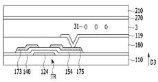
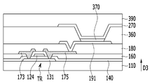
도 6은 도 1에서 A 영역의 단면의 일 실시예를 나타내고, 도 7은 도 1에서 화소 영역의 단면의 일 실시예를 나타낸다. 도 8은 도 1에서 A 영역의 단면의 일 실시예를 나타내고, 도 9는 도 1에서 화소 영역의 단면의 일 실시예를 나타낸다.
도 6 및 도 7은 표시 장치가 액정 표시 장치인 경우를 예로 들어 설명하기 위한 것이고, 도 8 및 도 9는 표시 장치가 유기 발광 표시 장치인 경우를 예로 들어 설명하기 위한 것이다. 하지만, 도 6의 구조 및 도 8의 구조는 표시 장치의 종류에 관계없이 적용될 수 있으며, 예컨대 도 6의 구조는 유기 발광 표시 장치에 적용될 수 있다.
도 6 및 도 8을 참고하면, 도 3과 비교하여 패드(P)의 구성 및 기판(110) 위에 존재할 수 있는 층 구조를 좀더 자세하게 도시하고 있다. 이방성 도전 필름(20) 및 연성 인쇄회로기판(50)의 특징은 도 3에 도시된 것과 실질적으로 동일하므로, 이에 대한 구체적인 설명은 생략한다.
도 6 및 도 7을 참고하면, 유리 또는 플라스틱 같은 기판(110) 위에 패드(P)의 제1 도전층(129)과 트랜지스터(TR)의 게이트 전극(124)이 위치한다. 제1 도전층(129) 및 게이트 전극(124)은 기판(110) 위에 구리(Cu), 알루미늄(Al), 은(Ag), 몰리브덴(Mo), 크롬(Cr), 탄탈륨(Ta), 티타늄(Ti) 같은 도전성 물질을 적층하고 패터닝하여 함께 형성될 수 있다.
제1 도전층(129) 및 게이트 전극(124) 위에는 게이트 절연층(140)이 위치한다. 게이트 절연층(140)은 산화 규소, 질화 규소 등의 무기 절연 물질을 적층하여 형성될 수 있다.
게이트 절연층(140) 위에는 트랜지스터(TR)의 반도체층(154)이 위치한다. 화소 영역에서 반도체층(154) 위에 트랜지스터(TR)의 소스 전극(173) 및 드레인 전극(175)이 위치하고, 패드 영역에서 게이트 절연층(140) 위에 제2 도전층(179)이 위치한다. 제2 도전층(179)은 제1 도전층(129)과 중첩하고, 게이트 절연층(140)에 형성된 접촉 구멍을 통해 제1 도전층(129)과 연결되어 있다. 제2 도전층(179), 소스 전극(173) 및 드레인 전극(175)은 구리(Cu), 알루미늄(Al), 은(Ag), 몰리브덴(Mo), 크롬(Cr), 금(Au), 백금(Pt), 팔라듐(Pd), 탄탈륨(Ta), 텅스텐(W), 티타늄(Ti), 니켈(Ni) 등의 도전성 물질을 적층하고 패터닝하여 함께 형성될 수 있다.
소소 전극(173) 및 드레인 전극(175) 위에는 유기 절연 물질 및/또는 무기 절연 물질을 포함할 수 있는 보호층(180)이 위치하고, 보호층(180) 위에는 인듐 주석 산화물(ITO), 인듐 아연 산화물(IZO) 같은 투명한 도전 물질을 포함할 수 있는 화소 전극(191)이 위치한다. 화소 전극(191)은 보호층(180)에 형성된 접촉 구멍을 통해 드레인 전극(175)과 연결되어 데이터 신호를 인가받을 수 있다. 화소 전극(191) 위에는 액정 분자들(31)을 포함하는 액정층(3)이 위치하고, 액정층(3) 위에는 기판(110)과 함께 액정층(3)을 밀봉하는 절연층(210)이 위치한다. 절연층(210)은 기판 형태일 수 있다.
절연층(210)의 아래에는 화소 전극(191)과 함께 액정층(3)에 전계를 생성하여 액정 분자들(31)의 배열 방향을 제어할 수 있는 공통 전극(270)이 위치한다. 화소 전극(191)과 액정층(3) 사이, 그리고 액정층(3)과 공통 전극(270) 사이에는 배향막(도시되지 않음)이 위치할 수 있다. 도시된 실시예와 달리, 공통 전극(270)은 기판(110)과 액정층(3) 사이에 위치할 수도 있다. 공통 전극(270)은 인듐 주석 산화물(ITO), 인듐 아연 산화물(IZO) 같은 투명한 도전 물질을 포함할 수 있다.
도 6에 도시된 패드 영역에서, 제1 및 제2 도전층(129, 179)을 포함하는 패드(P)에 연성 인쇄회로기판(50)이 이방성 도전 필름(20)을 통해 부착되므로, 표시 영역에 있는 액정층(3), 절연층(210) 등이 위치하지 않는다. 보호층(180)은 도시된 바와 같이 위치하지 않을 수 있고, 도시된 것과 달리 인접하는 패드들(P) 사이에 위치할 수도 있다. 패드(P)의 제2 도전층(179) 위에는 이와 중첩하면서 접촉하는 제3 도전층이 위치할 수 있고, 제3 도전층은 화소 전극(191)과 동일한 물질로 함께 형성될 수 있다.
도 8 및 도 9를 참고하면, 기판(110) 위에 트랜지스터(TR)의 반도체층(131)이 위치한다. 반도체층(131)은 소스 영역, 드레인 영역 및 이들 영역 사이의 채널 영역을 포함한다. 기판(110)과 반도체층(131) 사이에는 산소, 수분 등의 침투를 방지하기 위한 버퍼층(도시되지 않음)이 위치할 수 있다.
반도체층(131) 위로 게이트 절연층(140)이 위치한다. 게이트 절연층(140) 위에는 패드(P)의 제1 도전층(129)과 트랜지스터(TR)의 게이트 전극(124)이 위치한다. 제1 도전층(129) 및 게이트 전극(124)은 금속 등의 도전성 물질을 적층하고 패터닝하여 함께 형성될 수 있다. 게이트 절연층(140)이 기판(110)의 전면에 걸쳐 위치하는 것이 도시되어 있지만, 제1 도전층(129), 게이트 전극(124) 같은 게이트 도전체와 중첩하는 영역에만 위치할 수도 있다.
제1 도전층(129) 및 게이트 전극(124) 위에는 층간 절연층(160)이 위치한다. 층간 절연층(160) 위에는 패드(P)의 제2 도전층(179)과 트랜지스터(TR)의 소스 전극(173) 및 드레인 전극(175)이 위치한다. 제2 도전층(179)은 제1 도전층(129)과 중첩하고, 층간 절연층(160)에 형성된 접촉 구멍을 통해 제1 도전층(129)과 연결되어 있다. 소스 전극(173) 및 드레인 전극(175)은 층간 절연층(160) 및 게이트 절연층(140)에 형성된 접촉 구멍들을 통해 반도체층(131)의 소스 영역 및 드레인 전극과 각각 연결되어 있다.
소소 전극(173) 및 드레인 전극(175) 위에는 보호층(180)이 위치한다. 패드 영역에서 보호층(180)은 도시된 바와 같이 인접하는 패드들(P) 사이에 위치할 수 있다. 그러나 패드 영역에는 보호층(180)이 위치하지 않을 수도 있다. 보호층(180) 위에는 화소 전극(191)이 위치한다. 화소 전극(191)은 보호층(180)에 형성된 접촉 구멍을 통해 드레인 전극(175)과 연결되어 데이터 신호를 인가받을 수 있다.
보호층(180)과 화소 전극(191)의 일부 위에는 화소 정의막(360)이 위치한다. 화소 정의막(360)은 화소 전극(191)과 중첩하는 개구부를 가진다. 화소 정의막(360)의 개구부에는 화소 전극(191) 위로 발광층(370)이 위치하고, 발광층(370) 위에는 공통 전극(270)이 위치한다. 화소 전극(191), 발광층(370) 및 공통 전극(270)은 함께 유기 발광 다이오드를 구성한다. 화소 전극(191)은 유기 발광 다이오드의 애노드(anode)일 수 있고, 공통 전극(270)은 유기 발광 다이오드의 캐소드(cathode)일 수 있다. 공통 전극(270)의 위에는 유기 발광 다이오드를 보호하는 봉지층(encapsulation layer)(390)이 위치한다.
패드 영역에서, 패드(P) 위에는 범프들(B)을 포함하는 연성 인쇄회로기판(50)이 위치하고, 패드(P)와 연성 인쇄회로기판(50) 사이에는 이방성 도전 필름(20)이 위치한다. 이방성 도전 필름(20)은 전술한 바와 같이, 도전 입자들(CP)을 포함하는 지지층(21)과 그 위와 아래로 제1 접착층(22) 및 제2 접착층(23)을 포함한다. 패드(P)와 범프(B) 사이에서 이들과 중첩하게 위치하는 도전 입자들(CP)은 이들과 접촉하여 전기적으로 연결하고, 패드(P)와 범프(B) 사이에 위치하지 않는 도전 입자들(CP)은 절연되어 있다. 도전 입자들(CP)은 전체 영역에 걸쳐 균일하게 위치하고 있으므로, 이방성 도전 필름(20)의 신뢰성을 보증할 수 있다.
지금까지 연성 인쇄회로기판 같은 접속 부재와 표시 패널의 패드부 사이에 이방성 도전 필름이 적용되어 이들을 전기적으로, 물리적으로 연결하는 실시예들에 대해 살펴보았다. 이제 그러한 이방성 도전 필름 및 이를 제조하는 방법에 대해 도 10 내지 도 13을 참고하여 설명한다.
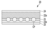
도 10은 본 발명의 일 실시예에 따른 이방성 도전 필름의 단면도이고, 도 11 내지 도 14는 도 10에 도시된 이방성 도전 필름을 제조하는 방법을 나타내는 공정 단면도이다.
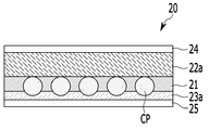
도 10을 참고하면, 본 발명의 일 실시예에 따른 이방성 도전 필름(20)이 도시된다. 이방성 도전 필름(20)은 도전 입자들(CP)을 포함하는 지지층(21), 지지층(21) 위의 제1 접착층(22a), 그리고 지지층(21) 아래의 제2 접착층(23a)을 포함한다. 제1 접착층(22a) 위에는 제1 이형지(24)가 위치하고 있고, 제2 접착층(23a)의 아래에는 제2 이형지(25)가 위치하고 있으며, 제1 및 제2 이형지들(24, 25)은 사용 시 제거될 수 있다. 제1 및 제2 이형지들(24, 25) 중 적어도 하나는 생략될 수 있다. 이방성 도전 필름(20)에서 도전 입자들(CP)을 제외한 나머지 구성요소들은 절연성일 수 있다.
지지층(21)은 경화 상태의 폴리머층이다. 지지층(21)은 경화 상태이기 때문에 지지층(21) 내의 도전 입자들(CP)을 고정할 수 있다. 지지층(21)은 중합되어 있기 때문에 이방성 도전 필름(20)의 적용 시 가열되어도 유동하기 어렵고, 따라서 지지층(21) 내의 도전 입자들(CP)도 유동하기 어렵다. 지지층(21)이 융점은 제1 및 제2 접착층(22a, 23b)의 경화점보다 높은 재료로 형성될 수 있다. 지지층(21)은 폴리이미드, 폴리에틸렌 테레프탈레이트, 나일론 6, 폴리비닐리덴 플로라이드, 폴라카보네이트, 폴리부틸렌 숙시네이트, 폴리에틸렌 중 적어도 하나를 포함할 수 있지만 이에 제한되지 않는다.
지지층(21) 위에 적층되어 있는 제1 접착층(22a)과 지지층(21) 아래에 적층되어 있는 제2 접착층(23a)은 미경화 상태의 수지층이다. 예컨대, 제1 접착층(22a) 및 제2 접착층(23a)은 열 경화성 수지층 또는 광 경화성 수지층일 수 있다. 제1 접착층(22a) 및 제2 접착층(23a)은 에폭시 화합물 또는 아크릴레이트 화합물과 중합 개시제를 함유하는 중합형 수지층일 수 있고, 중합 개시제는 이온 중합 개시제 또는 라디칼 중합 개시제일 수 있다. 제1 접착층(22a)과 제2 접착층(23a)은 서로 동일한 재료로 형성될 수 있고, 다른 재료로 형성될 수도 있다. 제1 접착층(22a)과 제2 접착층(23a) 중 적어도 하나는 에폭시 수지, 폴리에스테르 수지, 비스말레이미드 수지, 시아네이트 수지 등의 열경화성 수지일 수 있고, 반경화 상태일 수 있다. 제1 접착층(22a)은 제2 접착층(23a)보다 두꺼울 수 있다.
도 11 내지 도 14는 위와 같은 이방성 도전 필름(20)을 제조하는 공정이 도시된다.
도 11을 참고하면, 전사층(30)에 도전 입자들(CP)을 균등한 간격으로 단층으로 배열한다. 전사층(30) 상에 도전 입자들(CP)의 균등한 배열은 예컨대, 전사층(30) 상에 단층으로 도전 입자들(CP)을 배열한 후 전사층(30)을 1축 또는 2축 연신함으로써 이루어질 수 있다. 다른 예로서, 균일한 간격으로 홈들이 형성된 모판의 홈들에 도전 입자들(CP)을 채우고, 홈들에 배열된 도전 입자들(CP)을 전사층(30) 상에 전사함으로써 이루어질 수 있다.
도 12를 참고하면, 도전 입자들(CP)이 균등 간격으로 배열되어 있는 전사층(30) 위에 수지를 도포하여 도전 입자들(CP)이 함침되어 있는 수지층(21a)을 형성하고, 수지층(21a)을 경화시킨다. 이에 따라 전사층(30) 위에 있던 도전 입자들(CP)은 수지층(21a) 내로 전사되고 경화된 수지층(21a) 내에 균일한 간격을 유지한 채 고정된다. 그 후, 전사층(30)은 수지층(21a)으로부터 분리된다. 도전 입자들(CP)은 수지층(21a) 내부에 위치하여 수지층(21a)에 완전히 둘러싸여 있을 수 있지만, 도전 입자들(CP) 중 일부는 일부분인 수지층(21a)의 표면 밖으로 노출될 수 있다. 예컨대, 전사층(30)과 접하고 있던 도전 입자들(CP)의 부분은 수지층(21a)에 의해 둘러싸여 있지 않을 수 있다. 수지층(21a)의 두께는 도전 입자들(CP)의 직경보다 크지만, 거의 동일할 수도 있다.
도 13을 참고하면, 경화 상태의 수지층(21a)의 양쪽 표면을 식각하여, 도전 입자들(CP)의 일부분이 노출되어 있는 지지층(21)을 형성한다. 따라서 지지층(21)의 두께는 도전 입자들(CP)의 직경보다 작아질 수 있다. 도전 입자들(CP)은 지지층(21)의 상면과 하면으로부터 모두 돌출되게 노출될 수 있다. 도시된 것과 달리, 수지층(21a)의 상면(도 12에서 전사층(30)과 접하지 않는 면)만을 식각하여, 도전 입자들(CP)이 지지층(21)의 상면으로부터만 돌출될 수도 있다.
도전 입자들(CP)이 수지층(21a) 내부에 있을 경우, 수지층(21a)은 경화된 상태이기 때문에 이방성 도전막의 사용 시 가압하더라도 도전 입자들(CP)은 통전시켜야 할 전극들과 접촉하지 않고 수지층(21a)에 의해 절연되어 있을 수 있다. 수지층(21a)을 식각하여 도전 입자들(CP)을 수지층(21a) 외부로 노출시킴으로써, 도전 입자들(CP)은 지지층(21) 내에 고정되어 있으면서도 이방성 도전막의 두께 방향 도전성을 보증할 수 있다. 도전 입자들(CP)을 노출시키기 위한 수지층(21a)의 식각으로서 예컨대 반응성 이온 식각(reactive ion etching) 같은 건식 식각이 이용될 수 있지만, 이에 제한되는 것은 아니다.
도 14를 참고하면, 도전 입자들(CP)의 일부분이 노출되어 있는 지지층(21)의 상면에 제1 접착층(22)을 형성하고, 하면에 제2 접착층(23)을 형성한다. 제1 및 제2 접착층(22, 23)은 예컨대 지지층(21)에 미경화 수지층을 적층하거나(laminate) 미경화 수지를 코팅하여 형성될 수 있다. 적층 시, 미경화 수지층은 도 10에 도시된 이형지들(24, 25) 상에 형성되어 이형지들(24, 25)과 함께 지지층(21) 상에 적층될 수 있다.
위와 같이 형성된 이방성 도전 필름(20)은 도전 입자들(CP)이 지지층(21) 내에서 유동하지 않고 일정 간격으로 고정되어 있고, 이것은 이방성 도전 필름(20)을 사용하기 전은 물론이고 접속 부재를 접속시키기 위해 압착 또는 가열 압착된 후에도 동일하게 유지될 수 있다.
도 10에 도시된 이방성 도전 필름(20)은 도 3에 도시된 표시 장치에 적용되는 것일 수 있다. 도 4 및 도 5에 도시된 표시 장치들에 적용될 수 있는 이방성 도전 필름에 대해서는 도 15 및 도 16을 참고하여 설명한다.
도 15 및 도 16은 각각 본 발명의 일 실시예에 따른 이방성 도전 필름의 단면도이다.
도 15를 참고하면, 도 4에 도시된 표시 장치에 적용될 수 있는 이방성 도전 필름(10)이 도시된다. 도 10에 도시된 실시예와 마찬가지로, 이방성 도전 필름(20)은 도전 입자들(CP)을 포함하는 지지층(21), 지지층(21) 위의 제1 접착층(22a), 그리고 지지층(21) 아래의 제2 접착층(23a)을 포함한다. 제1 접착층(22a) 위에는 제1 이형지(24)가 위치하고 있고, 제2 접착층(23a)의 아래에는 제2 이형지(25)가 위치할 수 있다.
도전 입자들(CP)이 지지층(21)의 상면과 하면으로부터 모두 돌출되어 있는 도 10에 도시된 실시예와 달리, 본 실시예에서는 도전 입자들(CP)이 지지층(21)의 하면으로부터만 돌출되어 있다. 이와 같은 구조는 예컨대 도 12 및 도 13에 도시되는, 수지층(21a)을 식각하여 지지층(21)을 형성하는 공정에서 수지층(21a)의 상면만을 식각하고, 이에 의해 도전 입자들(CP)이 돌출되어 있는 지지층(21)의 표면에 제1 접착층(22)을 형성하고 도전 입자들(CP)이 돌출되어 있지 않은 지지층(21)의 표면에는 제2 접착층(23)을 형성함으로써 형성될 수 있다. 수지층(21a)의 한 면만이 식각되는 경우, 다른 면에서 도전 입자들(CP) 중 일부는 접착층(22)에 덮여 노출되어 있지 않은 상태일 수 있다. 그렇더라도 실제 적용 시, 예컨대 도 4에 도시된 제1 영역(R1)에서, 도전 입자들(CP)과 패드(P) 사이에 있을 수 있는 지지층(22)의 부분은 이방성 도전 필름(10)의 압착 시 가해지는 압력과 열에 의해 국소적으로 유동하여 도전 입자들(CP)과 패드(P) 사이에서 제거됨으로써 도전 입자들(CP)이 패드(P)와 집적 접촉할 수 있다.
도 16을 참고하면, 도 5에 도시된 표시 장치에 적용될 수 있는 이방성 도전 필름(10)이 도시된다. 도 15에 도시된 이방성 도전 필름(20)과 반대로, 제1 접착층(22a)이 형성되어 있는 지지층(21)의 상면으로부터 도전 입자들(CP)이 돌출되어 있지만, 지지층(22)의 하면으로부터는 도전 입자들(CP)이 돌출되어 있지 않다. 이러한 구조는 예컨대 도 12 및 도 13에 도시되는 수지층(21a)의 식각 시 수지층(21a) 상면만을 식각하여 지지층(21)을 형성하고 도전 입자들(CP)이 돌출되어 있는 지지층(21)의 표면에 제1 접착층(22a)을 형성함으로써 형성될 수 있다. 식각되지 않은 면에서 도전 입자들(CP)을 덮고 있을 수 있는 지지층(21)의 부분은 적용 시 열과 압력에 의해 국소적으로 이동할 수 있고, 따라서 도 5에 도시된 제1 영역(R1)에서 범프(B)와 도전 입자들(CP)이 직접 접촉할 수 있다.
도 17 및 도 18은 각각 본 발명의 일 실시예에 따른 도전 입자들의 배치를 나타낸 평면도이다.
도 17을 참고하면, 이방성 도전 필름(20)의 도전 입자들(CP)이 장방형으로 배치되어 있는 예가 도시된다. 즉, 도전 입자들(CP)은 x축 방향으로 제1 간격으로 배치되어 있고, x축 방향과 직교하는 y축 방향으로도 제1 간격으로 배치될 수 있다. 다른 예로, 도 18을 참고하면 도전 입자들(CP)은 마름모형으로 배치될 수 있다. 즉, 도전 입자들(CP)은 x축 방향으로 제1 간격으로 배치되고, x축 방향과 직교하는 y축 방향으로는 제1 간격과 다른 제2 간격으로 배치될 수 있다. 도전 입자들(CP) 간의 간격은 적용될 전극의 피치 및 폭을 고려하여 결정될 수 있다. 이와 같은 도전 입자들(CP)의 이방성 도전 필름(20) 내 균등 배치는 이방성 도전 필름(20)의 사용 전후에 걸쳐 유지될 수 있다.
이상에서 본 발명의 실시예에 대하여 상세하게 설명하였지만 본 발명의 권리범위는 이에 한정되는 것은 아니고 다음의 청구범위에서 정의하고 있는 본 발명의 기본 개념을 이용한 당업자의 여러 변형 및 개량 형태 또한 본 발명의 권리범위에 속하는 것이다.
10: 표시 패널
110: 기판
129: 제1 도전층 179: 제2 도전층
20: 이방성 도전 필름 21: 지지층
22: 제1 접착층 23: 제2 접착층
24: 제2 접착층 400: 집적회로 칩
50: 연성 인쇄회로기판 B: 범프
CP: 도전 입자 P: 패드
PP1: 제1 패드부 PP2: 제2 패드부
129: 제1 도전층 179: 제2 도전층
20: 이방성 도전 필름 21: 지지층
22: 제1 접착층 23: 제2 접착층
24: 제2 접착층 400: 집적회로 칩
50: 연성 인쇄회로기판 B: 범프
CP: 도전 입자 P: 패드
PP1: 제1 패드부 PP2: 제2 패드부
Claims (20)
- 기판 위에 위치하며 복수의 패드를 포함하는 패드부;
상기 패드부 위에 위치하는 이방성 도전 필름; 및
상기 이방성 도전 필름을 통해 상기 패드부에 부착되어 있으며, 복수의 범프를 포함하는 접속 부재;
를 포함하며,
상기 이방성 도전 필름은,
각각의 도전 입자의 일부분이 제1 면과 제2 면으로부터 돌출되어 있는 복수의 도전 입자를 포함하는 지지층;
상기 지지층의 상기 제1 면 및 상기 제1 면으로부터 돌출된 상기 도전 입자들의 부분과 접촉하는 제1 접착층; 및
상기 지지층의 상기 제2 면 및 상기 제2 면으로부터 돌출된 상기 도전 입자들의 부분과 접촉하는 제2 접착층;
을 포함하고, 상기 제1 접착층 및 상기 제2 접착층 중 적어도 하나는 상기 패드들과 상기 범퍼들이 중첩하는 제1 영역과 상기 패드들과 상기 범퍼들이 중첩하지 않는 제2 영역에 모두 위치하는 표시 장치. - 제1항에서,
상기 지지층은 상기 제1 접착층 및 상기 제2 접착층과 상이한 재료로 형성되어 있는 표시 장치. - 제2항에서,
상기 지지층은 폴리이미드, 폴리에틸렌 테레프탈레이트, 나일론 6, 폴리비닐리덴 플로라이드, 폴라카보네이트, 폴리부틸렌 숙시네이트 및 폴리에틸렌으로 이루어진 그룹에서 선택된 적어도 하나의 폴리머를 포함하는 표시 장치. - 제1항에서,
상기 지지층의 융점이 상기 제1 접착층의 경화점 및 상기 제2 접착층의 경화점보다 높은 표시 장치. - 제1항에서,
제1 방향으로 인접하는 도전 입자들 사이의 간격이 상기 제1 영역과 상기 제2 영역에서 일정한 표시 장치. - 제5항에서,
상기 제1 방향과 교차하는 제2 방향으로 인접하는 도전 입자들 사이의 간격이 상기 제1 영역과 상기 제2 영역에서 일정한 표시 장치. - 제5항에서,
상기 복수의 도전 입자는 평면도에서 장방형 또는 마름모형으로 배열되어 있는 표시 장치. - 제1항에서,
상기 복수의 도전 입자의 직경이 상기 지지층의 두께보다 큰 표시 장치. - 제1항에서,
상기 제1 접착층은 상기 제1 영역에 위치하는 부분의 두께가 상기 제2 영역에 위치하는 부분의 두께보다 작은 표시 장치. - 제1항에서,
상기 제2 접착층은 상기 제1 영역에 위치하는 부분의 두께가 상기 제2 영역에 위치하는 부분의 두께보다 작은 표시 장치. - 미경화 수지층에 도전 입자들을 배열하는 단계;
상기 수지층을 경화시켜 상기 도전 입자들을 경화된 수지층 내에 고정하는 단계; 및
상기 경화된 수지층을 식각하여 상기 도전 입자들의 일부분을 노출시키는 지지체를 형성하는 단계;
를 포함하는 이방성 도전 필름의 제조 방법. - 제11항에서,
상기 식각은 상기 지지체의 적어도 한 면에서 상기 도전 입자들의 일부분을 노출시키는 것을 포함하는 이방성 도전 필름의 제조 방법. - 제11항에서,
상기 식각은 반응성 이온 식각을 포함하는 이방성 도전 필름의 제조 방법. - 제11항에서,
상기 지지층은 폴리이미드, 폴리에틸렌 테레프탈레이트, 나일론 6, 폴리비닐리덴 플로라이드, 폴라카보네이트, 폴리부틸렌 숙시네이트 및 폴리에틸렌으로 이루어진 그룹에서 선택된 적어도 하나의 폴리머를 포함하는 이방성 도전 필름의 제조 방법. - 제11항에서,
상기 지지체의 상기 양면 중 적어도 한 면에 접착층을 형성하는 단계를 더 포함하는 이방성 도전 필름의 제조 방법. - 제15항에서,
상기 접착층은 상기 도전 입자들의 노출된 부분에 접촉하게 형성되는 이방성 도전 필름의 제조 방법. - 제15항에서,
상기 접착층은 상기 지지체 위에 미경화 수지층을 적층하여 형성되는 이방성 도전 필름의 형성 방법. - 제15항에서,
상기 접착층은 상기 지지층과 상이한 재료로 형성되는 이방성 도전 필름의 제조 방법. - 제15항에서,
상기 지지층의 융점이 상기 접착층의 경화점보다 높은 이방성 도전 필름의 제조 방법. - 제11항에서,
상기 지지층은 각각의 도전 입자의 직경보다 작은 두께로 형성되는 이방성 도전 필름의 제조 방법.
Priority Applications (3)
| Application Number | Priority Date | Filing Date | Title |
|---|---|---|---|
| KR1020160060271A KR20170130003A (ko) | 2016-05-17 | 2016-05-17 | 이방성 도전 필름을 포함하는 표시 장치 및 이방성 도전 필름의 제조 방법 |
| US15/365,979 US20170338198A1 (en) | 2016-05-17 | 2016-12-01 | Display device including an anisotropic conductive film, and manufacturing method of the anisotropic conductive film |
| CN201710342057.3A CN107393895A (zh) | 2016-05-17 | 2017-05-16 | 显示装置 |
Applications Claiming Priority (1)
| Application Number | Priority Date | Filing Date | Title |
|---|---|---|---|
| KR1020160060271A KR20170130003A (ko) | 2016-05-17 | 2016-05-17 | 이방성 도전 필름을 포함하는 표시 장치 및 이방성 도전 필름의 제조 방법 |
Publications (1)
| Publication Number | Publication Date |
|---|---|
| KR20170130003A true KR20170130003A (ko) | 2017-11-28 |
Family
ID=60330823
Family Applications (1)
| Application Number | Title | Priority Date | Filing Date |
|---|---|---|---|
| KR1020160060271A KR20170130003A (ko) | 2016-05-17 | 2016-05-17 | 이방성 도전 필름을 포함하는 표시 장치 및 이방성 도전 필름의 제조 방법 |
Country Status (3)
| Country | Link |
|---|---|
| US (1) | US20170338198A1 (ko) |
| KR (1) | KR20170130003A (ko) |
| CN (1) | CN107393895A (ko) |
Cited By (6)
| Publication number | Priority date | Publication date | Assignee | Title |
|---|---|---|---|---|
| KR101964881B1 (ko) * | 2018-01-17 | 2019-04-02 | 울산과학기술원 | 상온 액체 금속 캡슐을 이용하여 디바이스를 치유하는 신축성 패키지 및 이의 제조방법 |
| KR20190115163A (ko) * | 2018-03-30 | 2019-10-11 | 삼성디스플레이 주식회사 | 표시 장치 |
| US11145706B2 (en) | 2019-06-21 | 2021-10-12 | Samsung Display Co., Ltd. | Display device and method of manufacturing the same |
| US11209875B2 (en) | 2019-08-09 | 2021-12-28 | Samsung Display Co., Ltd. | Adhesive member and display device including the same |
| US11419216B2 (en) | 2020-03-30 | 2022-08-16 | Samsung Display Co., Ltd. | Display device and method of manufacturing the same |
| US11824034B2 (en) | 2020-03-10 | 2023-11-21 | Samsung Display Co., Ltd. | Display device including adhesive film with conductive ball |
Families Citing this family (12)
| Publication number | Priority date | Publication date | Assignee | Title |
|---|---|---|---|---|
| US20170338204A1 (en) * | 2016-05-17 | 2017-11-23 | Taiwan Semiconductor Manufacturing Company, Ltd. | Device and Method for UBM/RDL Routing |
| KR102487061B1 (ko) * | 2016-06-30 | 2023-01-12 | 삼성디스플레이 주식회사 | 표시 장치 |
| JP2018054678A (ja) * | 2016-09-26 | 2018-04-05 | 株式会社ジャパンディスプレイ | 表示装置及びその製造方法 |
| CN108987439A (zh) * | 2018-06-21 | 2018-12-11 | 武汉华星光电半导体显示技术有限公司 | 显示面板和显示装置 |
| KR102629350B1 (ko) * | 2018-12-12 | 2024-01-25 | 삼성디스플레이 주식회사 | 표시 장치 및 그 제조 방법 |
| KR20210090753A (ko) * | 2020-01-10 | 2021-07-21 | 삼성디스플레이 주식회사 | 표시패널, 표시패널의 제조 방법, 및 이를 포함한 표시장치 |
| KR20210152066A (ko) * | 2020-06-05 | 2021-12-15 | 삼성디스플레이 주식회사 | 표시장치 및 이의 제조 방법 |
| TWI730819B (zh) * | 2020-06-19 | 2021-06-11 | 元太科技工業股份有限公司 | 電子裝置 |
| CN113823637A (zh) * | 2020-06-19 | 2021-12-21 | 元太科技工业股份有限公司 | 电子装置 |
| CN113451491B (zh) * | 2020-09-29 | 2022-04-29 | 重庆康佳光电技术研究院有限公司 | 显示面板及其制作方法 |
| KR20220062156A (ko) * | 2020-11-06 | 2022-05-16 | 삼성디스플레이 주식회사 | 표시 장치 및 표시 장치의 제조 방법 |
| KR20220099200A (ko) * | 2021-01-05 | 2022-07-13 | 삼성디스플레이 주식회사 | 접착 부재, 표시 장치 및 표시 장치 제조 방법 |
Family Cites Families (7)
| Publication number | Priority date | Publication date | Assignee | Title |
|---|---|---|---|---|
| TW277152B (ko) * | 1994-05-10 | 1996-06-01 | Hitachi Chemical Co Ltd | |
| US20070212521A1 (en) * | 2004-03-30 | 2007-09-13 | Tokai Rubber Industries, Ltd. | Anisotropic Conductive Film and a Method of Manufacturing the Same |
| JP2008027676A (ja) * | 2006-07-19 | 2008-02-07 | Tokai Rubber Ind Ltd | 異方性導電膜の製造方法および異方性導電膜 |
| KR101568659B1 (ko) * | 2013-03-29 | 2015-11-12 | 제일모직주식회사 | 도전성 접착층을 포함하는 이방 도전성 필름 및 상기 필름에 의해 접속된 반도체 장치 |
| JP6273875B2 (ja) * | 2014-02-04 | 2018-02-07 | デクセリアルズ株式会社 | 異方性導電フィルム及びその製造方法 |
| JP2015167106A (ja) * | 2014-03-04 | 2015-09-24 | 日立化成株式会社 | 異方導電性フィルム及び接続構造体 |
| JP6690184B2 (ja) * | 2014-10-28 | 2020-04-28 | デクセリアルズ株式会社 | 異方導電性フィルム及び接続構造体 |
-
2016
- 2016-05-17 KR KR1020160060271A patent/KR20170130003A/ko not_active IP Right Cessation
- 2016-12-01 US US15/365,979 patent/US20170338198A1/en not_active Abandoned
-
2017
- 2017-05-16 CN CN201710342057.3A patent/CN107393895A/zh active Pending
Cited By (7)
| Publication number | Priority date | Publication date | Assignee | Title |
|---|---|---|---|---|
| KR101964881B1 (ko) * | 2018-01-17 | 2019-04-02 | 울산과학기술원 | 상온 액체 금속 캡슐을 이용하여 디바이스를 치유하는 신축성 패키지 및 이의 제조방법 |
| KR20190115163A (ko) * | 2018-03-30 | 2019-10-11 | 삼성디스플레이 주식회사 | 표시 장치 |
| US11145706B2 (en) | 2019-06-21 | 2021-10-12 | Samsung Display Co., Ltd. | Display device and method of manufacturing the same |
| US11856828B2 (en) | 2019-06-21 | 2023-12-26 | Samsung Display Co., Ltd. | Display device and method of manufacturing the same |
| US11209875B2 (en) | 2019-08-09 | 2021-12-28 | Samsung Display Co., Ltd. | Adhesive member and display device including the same |
| US11824034B2 (en) | 2020-03-10 | 2023-11-21 | Samsung Display Co., Ltd. | Display device including adhesive film with conductive ball |
| US11419216B2 (en) | 2020-03-30 | 2022-08-16 | Samsung Display Co., Ltd. | Display device and method of manufacturing the same |
Also Published As
| Publication number | Publication date |
|---|---|
| US20170338198A1 (en) | 2017-11-23 |
| CN107393895A (zh) | 2017-11-24 |
Similar Documents
| Publication | Publication Date | Title |
|---|---|---|
| KR20170130003A (ko) | 이방성 도전 필름을 포함하는 표시 장치 및 이방성 도전 필름의 제조 방법 | |
| KR101908501B1 (ko) | 터치 스크린 일체형 유기 발광 표시 장치 및 이의 제조 방법 | |
| JP3139549B2 (ja) | アクティブマトリクス型液晶表示装置 | |
| US20150085527A1 (en) | Light source module, fabrication method therefor, and backlight unit including the same | |
| US8127438B2 (en) | Wiring substrate, method of manufacturing wiring substrate, and electronic apparatus | |
| KR20170139217A (ko) | 표시장치 및 이의 제조방법 | |
| US20100071946A1 (en) | Electronic component mounting structure | |
| KR20180050438A (ko) | 이방성 도전 필름, 이방성 도전 필름의 제조 방법, 접속체의 제조 방법 및 접속 방법 | |
| KR100707587B1 (ko) | 전자 부품 실장체의 제조 방법 및 전기 광학 장치 | |
| JP5125314B2 (ja) | 電子装置 | |
| US11579501B2 (en) | LCOS structure and method of forming same | |
| JP2013030789A (ja) | 実装構造体及び実装構造体の製造方法 | |
| JP2009054833A (ja) | 電子デバイスとその製造方法、電気光学装置および電子機器 | |
| KR20000062451A (ko) | 영상 장치 및 그 제조 방법 | |
| US20180011369A1 (en) | Display device having a connection member secured in place by a conductive layer | |
| KR20040050245A (ko) | 박막 트랜지스터 기판, 이의 제조방법, 이를 갖는액정표시장치 및 이의 제조방법 | |
| JP2018073246A (ja) | 表示装置 | |
| CN111540754A (zh) | 微型发光二极管显示面板及其制作方法、显示装置 | |
| JP2008118056A (ja) | 配線基板の製造方法および電子機器 | |
| KR102579426B1 (ko) | 표시 장치 및 그 제조 방법 | |
| US11803086B2 (en) | Electronic device and manufacturing method thereof | |
| JP4844738B2 (ja) | 配線基板の製造方法 | |
| US20180033755A1 (en) | Integrated circuit chip and display device including the same | |
| JP2009049154A (ja) | 半導体装置、実装構造体、電気光学装置、電子機器 | |
| JP2008159733A (ja) | 電子部品実装体の製造方法、電子部品実装体、及び、電気光学装置の製造方法 |
Legal Events
| Date | Code | Title | Description |
|---|---|---|---|
| A201 | Request for examination | ||
| AMND | Amendment | ||
| E601 | Decision to refuse application | ||
| AMND | Amendment | ||
| X601 | Decision of rejection after re-examination |