KR20170032455A - Conductive material for connection parts which has excellent minute slide wear resistance - Google Patents
Conductive material for connection parts which has excellent minute slide wear resistance Download PDFInfo
- Publication number
- KR20170032455A KR20170032455A KR1020177004996A KR20177004996A KR20170032455A KR 20170032455 A KR20170032455 A KR 20170032455A KR 1020177004996 A KR1020177004996 A KR 1020177004996A KR 20177004996 A KR20177004996 A KR 20177004996A KR 20170032455 A KR20170032455 A KR 20170032455A
- Authority
- KR
- South Korea
- Prior art keywords
- coating layer
- mass
- alloy
- alloy coating
- layer
- Prior art date
Links
Images


Classifications
-
- C—CHEMISTRY; METALLURGY
- C25—ELECTROLYTIC OR ELECTROPHORETIC PROCESSES; APPARATUS THEREFOR
- C25D—PROCESSES FOR THE ELECTROLYTIC OR ELECTROPHORETIC PRODUCTION OF COATINGS; ELECTROFORMING; APPARATUS THEREFOR
- C25D5/00—Electroplating characterised by the process; Pretreatment or after-treatment of workpieces
- C25D5/48—After-treatment of electroplated surfaces
- C25D5/50—After-treatment of electroplated surfaces by heat-treatment
- C25D5/505—After-treatment of electroplated surfaces by heat-treatment of electroplated tin coatings, e.g. by melting
-
- C—CHEMISTRY; METALLURGY
- C22—METALLURGY; FERROUS OR NON-FERROUS ALLOYS; TREATMENT OF ALLOYS OR NON-FERROUS METALS
- C22C—ALLOYS
- C22C9/00—Alloys based on copper
- C22C9/02—Alloys based on copper with tin as the next major constituent
-
- C—CHEMISTRY; METALLURGY
- C22—METALLURGY; FERROUS OR NON-FERROUS ALLOYS; TREATMENT OF ALLOYS OR NON-FERROUS METALS
- C22C—ALLOYS
- C22C13/00—Alloys based on tin
-
- C—CHEMISTRY; METALLURGY
- C22—METALLURGY; FERROUS OR NON-FERROUS ALLOYS; TREATMENT OF ALLOYS OR NON-FERROUS METALS
- C22C—ALLOYS
- C22C9/00—Alloys based on copper
-
- C—CHEMISTRY; METALLURGY
- C22—METALLURGY; FERROUS OR NON-FERROUS ALLOYS; TREATMENT OF ALLOYS OR NON-FERROUS METALS
- C22C—ALLOYS
- C22C9/00—Alloys based on copper
- C22C9/01—Alloys based on copper with aluminium as the next major constituent
-
- C—CHEMISTRY; METALLURGY
- C22—METALLURGY; FERROUS OR NON-FERROUS ALLOYS; TREATMENT OF ALLOYS OR NON-FERROUS METALS
- C22C—ALLOYS
- C22C9/00—Alloys based on copper
- C22C9/04—Alloys based on copper with zinc as the next major constituent
-
- C—CHEMISTRY; METALLURGY
- C22—METALLURGY; FERROUS OR NON-FERROUS ALLOYS; TREATMENT OF ALLOYS OR NON-FERROUS METALS
- C22C—ALLOYS
- C22C9/00—Alloys based on copper
- C22C9/05—Alloys based on copper with manganese as the next major constituent
-
- C—CHEMISTRY; METALLURGY
- C22—METALLURGY; FERROUS OR NON-FERROUS ALLOYS; TREATMENT OF ALLOYS OR NON-FERROUS METALS
- C22C—ALLOYS
- C22C9/00—Alloys based on copper
- C22C9/06—Alloys based on copper with nickel or cobalt as the next major constituent
-
- C—CHEMISTRY; METALLURGY
- C22—METALLURGY; FERROUS OR NON-FERROUS ALLOYS; TREATMENT OF ALLOYS OR NON-FERROUS METALS
- C22C—ALLOYS
- C22C9/00—Alloys based on copper
- C22C9/10—Alloys based on copper with silicon as the next major constituent
-
- C—CHEMISTRY; METALLURGY
- C23—COATING METALLIC MATERIAL; COATING MATERIAL WITH METALLIC MATERIAL; CHEMICAL SURFACE TREATMENT; DIFFUSION TREATMENT OF METALLIC MATERIAL; COATING BY VACUUM EVAPORATION, BY SPUTTERING, BY ION IMPLANTATION OR BY CHEMICAL VAPOUR DEPOSITION, IN GENERAL; INHIBITING CORROSION OF METALLIC MATERIAL OR INCRUSTATION IN GENERAL
- C23C—COATING METALLIC MATERIAL; COATING MATERIAL WITH METALLIC MATERIAL; SURFACE TREATMENT OF METALLIC MATERIAL BY DIFFUSION INTO THE SURFACE, BY CHEMICAL CONVERSION OR SUBSTITUTION; COATING BY VACUUM EVAPORATION, BY SPUTTERING, BY ION IMPLANTATION OR BY CHEMICAL VAPOUR DEPOSITION, IN GENERAL
- C23C28/00—Coating for obtaining at least two superposed coatings either by methods not provided for in a single one of groups C23C2/00 - C23C26/00 or by combinations of methods provided for in subclasses C23C and C25C or C25D
- C23C28/02—Coating for obtaining at least two superposed coatings either by methods not provided for in a single one of groups C23C2/00 - C23C26/00 or by combinations of methods provided for in subclasses C23C and C25C or C25D only coatings only including layers of metallic material
- C23C28/021—Coating for obtaining at least two superposed coatings either by methods not provided for in a single one of groups C23C2/00 - C23C26/00 or by combinations of methods provided for in subclasses C23C and C25C or C25D only coatings only including layers of metallic material including at least one metal alloy layer
-
- C—CHEMISTRY; METALLURGY
- C25—ELECTROLYTIC OR ELECTROPHORETIC PROCESSES; APPARATUS THEREFOR
- C25D—PROCESSES FOR THE ELECTROLYTIC OR ELECTROPHORETIC PRODUCTION OF COATINGS; ELECTROFORMING; APPARATUS THEREFOR
- C25D5/00—Electroplating characterised by the process; Pretreatment or after-treatment of workpieces
- C25D5/10—Electroplating with more than one layer of the same or of different metals
- C25D5/12—Electroplating with more than one layer of the same or of different metals at least one layer being of nickel or chromium
-
- C—CHEMISTRY; METALLURGY
- C25—ELECTROLYTIC OR ELECTROPHORETIC PROCESSES; APPARATUS THEREFOR
- C25D—PROCESSES FOR THE ELECTROLYTIC OR ELECTROPHORETIC PRODUCTION OF COATINGS; ELECTROFORMING; APPARATUS THEREFOR
- C25D5/00—Electroplating characterised by the process; Pretreatment or after-treatment of workpieces
- C25D5/48—After-treatment of electroplated surfaces
- C25D5/50—After-treatment of electroplated surfaces by heat-treatment
-
- C—CHEMISTRY; METALLURGY
- C25—ELECTROLYTIC OR ELECTROPHORETIC PROCESSES; APPARATUS THEREFOR
- C25D—PROCESSES FOR THE ELECTROLYTIC OR ELECTROPHORETIC PRODUCTION OF COATINGS; ELECTROFORMING; APPARATUS THEREFOR
- C25D5/00—Electroplating characterised by the process; Pretreatment or after-treatment of workpieces
- C25D5/60—Electroplating characterised by the structure or texture of the layers
- C25D5/605—Surface topography of the layers, e.g. rough, dendritic or nodular layers
-
- C—CHEMISTRY; METALLURGY
- C25—ELECTROLYTIC OR ELECTROPHORETIC PROCESSES; APPARATUS THEREFOR
- C25D—PROCESSES FOR THE ELECTROLYTIC OR ELECTROPHORETIC PRODUCTION OF COATINGS; ELECTROFORMING; APPARATUS THEREFOR
- C25D5/00—Electroplating characterised by the process; Pretreatment or after-treatment of workpieces
- C25D5/60—Electroplating characterised by the structure or texture of the layers
- C25D5/615—Microstructure of the layers, e.g. mixed structure
- C25D5/617—Crystalline layers
-
- C—CHEMISTRY; METALLURGY
- C25—ELECTROLYTIC OR ELECTROPHORETIC PROCESSES; APPARATUS THEREFOR
- C25D—PROCESSES FOR THE ELECTROLYTIC OR ELECTROPHORETIC PRODUCTION OF COATINGS; ELECTROFORMING; APPARATUS THEREFOR
- C25D7/00—Electroplating characterised by the article coated
-
- H—ELECTRICITY
- H01—ELECTRIC ELEMENTS
- H01B—CABLES; CONDUCTORS; INSULATORS; SELECTION OF MATERIALS FOR THEIR CONDUCTIVE, INSULATING OR DIELECTRIC PROPERTIES
- H01B5/00—Non-insulated conductors or conductive bodies characterised by their form
- H01B5/02—Single bars, rods, wires, or strips
-
- H—ELECTRICITY
- H01—ELECTRIC ELEMENTS
- H01R—ELECTRICALLY-CONDUCTIVE CONNECTIONS; STRUCTURAL ASSOCIATIONS OF A PLURALITY OF MUTUALLY-INSULATED ELECTRICAL CONNECTING ELEMENTS; COUPLING DEVICES; CURRENT COLLECTORS
- H01R13/00—Details of coupling devices of the kinds covered by groups H01R12/70 or H01R24/00 - H01R33/00
- H01R13/02—Contact members
- H01R13/03—Contact members characterised by the material, e.g. plating, or coating materials
Abstract
본 발명의 접속 부품용 도전 재료는, Cr과 Zr, Fe와 P, 또는 Zn을 각각 특정량 함유하는 구리 합금으로 이루어지는 모재의 표면에, Cu 함유량이 20∼70at%이고, 평균 두께가 0.2∼3.0μm인 Cu-Sn 합금 피복층과, 평균 두께가 0.05∼5.0μm인 Sn 피복층이 형성되어 있다.The conductive material for a connecting part of the present invention is characterized in that the surface of a base material made of a copper alloy containing a specific amount of Cr and Zr, Fe and P or Zn respectively has a Cu content of 20 to 70 at% and an average thickness of 0.2 to 3.0 mu m and a Sn coating layer having an average thickness of 0.05 to 5.0 mu m are formed.
Description
본 발명은, 주로 자동차 분야나 일반 민생 분야에서 이용되는 단자 등의 접속 부품용 도전 재료에 관한 것으로, 특히 구리 합금을 모재로 하고, 미세접동(摺動) 마모를 저감할 수 있는 Sn 도금 부착 접속 부품용 도전 재료에 관한 것이다.TECHNICAL FIELD The present invention relates to a conductive material for connecting parts such as terminals mainly used in the fields of automobiles and general welfare. Especially, the present invention relates to a conductive material for a connecting part such as a terminal with a Sn-plated connection which is made of a copper alloy as a base material and can reduce sliding abrasion And a conductive material for parts.
자동차의 엔진을 전자적으로 제어하는 기기(ECU: Electronic Control Unit) 등에 이용되는 다극 커넥터용 감합(嵌合) 단자의 소재로서, Cu-Ni-Si계, Cu-Ni-Sn-P계, Cu-Fe-P계, Cu-Zn계 등, 여러 가지의 구리 합금이 이용되고 있다. 감합 단자는 수컷 단자와 암컷 단자로 구성되는데, 감합 단자의 용도, 사용 환경, 가격 등을 고려하여 수컷 단자와 암컷 단자에는 통상은 다른 구리 합금을 이용하는 것이 일반적이다.A Cu-Ni-Si alloy, a Cu-Ni-Sn-P alloy, a Cu-Ni-Sn-P alloy, or a Cu-Ni-Si alloy is used as a material of a fitting terminal for a multipolar connector used in an electronic control unit (ECU) Fe-P alloy, Cu-Zn alloy, and the like. The fitting terminal is composed of a male terminal and a female terminal. Generally, a copper alloy is usually used for the male terminal and the female terminal in consideration of the use, the use environment, and the price of the fitting terminal.
이 중 Cu-Ni-Si계 합금은, 600MPa 이상의 인장 강도, 중간 정도의 도전율(25∼50% IACS), 및 0.2% 내력의 80%의 굽힘 응력 부하 상태로 150℃×1000시간 유지 후의 응력 완화율이 15∼20% 정도인 특성을 가져, 강도와 내응력완화특성이 우수하다.Of these, the Cu-Ni-Si alloy has a tensile strength of 600 MPa or more, a moderate conductivity (25 to 50% IACS), and a stress relaxation after maintaining at 150 占 폚 for 1000 hours under a bending stress load of 80% Rate is about 15 to 20%, and the strength and the stress relaxation property are excellent.
Cu-Fe-P계 합금으로서 C19210, C194 등이 알려져 있지만, 이들 Cu-Fe-P계 합금은 인장 강도 400∼600MPa 정도, 도전율 60∼90% IACS, 상기 조건에 있어서의 응력 완화율이 60% 이하인 특성을 갖는다. 한편, 감합 단자에 있어서, 내응력완화특성이 요구되는 것은 암컷 단자이며, 통상, 상기 조건에서의 응력 완화율이 25% 이하인 구리 합금이 선정된다. 또한, Cu-Fe-P계 합금은, Cu-Ni-Si계 합금이나 황동보다 도전율이 높아, 단자를 소형화(수컷-암컷 단자간의 접촉 면적이 작아진다)하더라도, 온도 상승의 억제에 유리하다. 또한, 응력 완화율이 황동보다 15% 이상 작다. 게다가, Sn을 선도금한 구리 합금조(條)를 타발 가공하여 제작한 단자의 타발 가공면은 모재가 노출되지만, Fe를 포함하는 합금 원소의 총함유량이 2.5질량% 이하인 Cu-Fe-P계 합금의 경우, 노출 부분의 땜납 젖음성이 우수하여, Sn을 후도금하는 일 없이 납땜이 가능하다. Cu-Fe-P계 합금에는 이와 같은 이점이 있기 때문에, 특히 소형의 감합 단자용, 나아가서는 그 중에서도 내응력완화특성을 그만큼 필요로 하지 않는 수컷 단자용으로서 이용되게 되었다.These Cu-Fe-P based alloys have a tensile strength of about 400 to 600 MPa, an electrical conductivity of 60 to 90% IACS, a stress relaxation rate of 60% or more under the above conditions, Or less. On the other hand, in the fitting terminal, it is the female terminal which requires the stress relaxation property, and a copper alloy having a stress relaxation rate of 25% or less under the above conditions is usually selected. The Cu-Fe-P alloy has a higher conductivity than the Cu-Ni-Si alloy or brass and is advantageous in suppressing the temperature rise even when the terminal is miniaturized (the contact area between the male and female terminals is small). Also, the stress relaxation rate is 15% smaller than that of brass. In addition, the punching surface of the terminal produced by punching the copper alloy lead wire which has been subjected to Sn is exposed to the Cu-Fe-P alloy having a total content of the alloy elements containing Fe of 2.5% by mass or less In the case of the alloy, the solder wettability of the exposed portion is excellent, and soldering is possible without post plating the Sn. Since the Cu-Fe-P alloy has such an advantage, the Cu-Fe-P alloy is used particularly for a small fitting terminal, and more particularly, for a male terminal which does not require the stress relaxation property as much.
Cu-Zn계로서는, Zn을 10∼40%(질량%, 이하 동일) 포함하는 Cu-Zn 합금이 C2200(10% Zn), C2300(15% Zn), C2400(20% Zn), C2600(30% Zn), C2700(35% Zn), C2801(40% Zn)로서, JIS H 3100에 규정되어 있다. 이들 Cu-Zn 합금은 단동(丹銅), 황동이라고 불리고 있다. 그리고, 이들 Cu-Zn 합금은 중간 정도의 도전율(25∼45% IACS)을 가져, 강도와 연성(굽힘 가공성)의 밸런스가 좋고, 스프링 한계값이 높다. 상기 조건에 있어서의 응력 완화율이 50%를 초과한다. 또한, Cu보다 가격이 저렴한 Zn을 많이 함유하고, 또한 가공 열처리 공정이 비교적 단순하기 때문에, 가격이 저렴하다. Cu-Zn계 합금에는 이와 같은 이점이 있기 때문에, 소형의 감합 단자용, 나아가서는 그 중에서도 내응력완화특성을 그만큼 필요로 하지 않는 수컷 단자용으로서 이용되고 있다.As the Cu-Zn system, a Cu-Zn alloy containing 10 to 40% (by mass,% or less) of Zn is C2200 (10% Zn), C2300 (15% Zn), C2400 (20% Zn) % Zn), C2700 (35% Zn) and C2801 (40% Zn), which are specified in JIS H 3100. These Cu-Zn alloys are called dandong copper and brass. These Cu-Zn alloys have a medium conductivity (25 to 45% IACS), good balance of strength and ductility (bending workability), and high spring limit value. The stress relaxation rate under the above conditions exceeds 50%. In addition, since it contains a large amount of Zn which is cheaper than Cu and the process heat treatment process is relatively simple, the price is low. Since Cu-Zn alloy has such an advantage, it is used for a small fitting terminal, and more particularly for a male terminal which does not require the stress relaxation property so much.
또한, 감합 단자에는, 내식성 확보 및 접촉부에 있어서의 접촉 저항 저감 등을 위해, 표면에 두께 1μm 정도의 Sn 피복층(리플로 Sn 도금 등)이 설치된다. Sn 피복층을 형성한 감합 단자에서는, 수컷 단자를 암컷 단자에 삽입할 때, 연질인 Sn 피복층(Hv: 10∼30 정도)이 소성 변형되어, 수컷-암컷 단자간에 생긴 Sn-Sn의 응착부가 전단된다. 이때 발생하는 변형 저항 및 전단 저항에 의해, Sn 피복층을 형성한 감합 단자에서는, 단자의 삽입력이 커진다. 상기 ECU는, 다수의 감합 단자를 수용하는 커넥터에 의해 접속되기 때문에, 국수(局數)의 증대에 수반하여 접속 시의 삽입력이 커진다. 따라서, 작업자의 부담의 경감, 접속의 완전성 확보 등의 관점에서, 감합 단자의 삽입력 저감이 요구되고 있다.An Sn coating layer (reflowed Sn plating or the like) having a thickness of about 1 mu m is provided on the surface of the fitting terminal for securing corrosion resistance and reducing contact resistance at the contact portion. In the fitting terminal where the Sn coating layer is formed, when the male terminal is inserted into the female terminal, the soft Sn coating layer (Hv: about 10 to 30) is plastically deformed to shear the Sn-Sn adhesion portion formed between the male and female terminals . Due to the deformation resistance and shear resistance generated at this time, the insertion force of the terminal becomes large at the fitting terminal in which the Sn coating layer is formed. Since the ECU is connected by a connector that accommodates a plurality of mating terminals, the insertion force at the time of connection increases with the increase in the number of stations. Therefore, from the viewpoints of reducing the burden on the operator, securing the integrity of the connection, and the like, it is required to reduce the insertion force of the fitting terminal.
단자 감합 후에 있어서는, 미세접동 마모 현상이 문제가 된다. 미세접동 마모 현상이란, 자동차의 엔진의 진동이나 주행 시의 진동 및 분위기 온도의 변동에 수반하는 팽창, 수축 등에 의해, 수컷 단자와 암컷 단자간에 접동이 발생하고, 이에 의해 단자 표면의 Sn 도금이 마모되는 현상이다. 미세접동 마모 현상으로 생긴 Sn의 마모 분말이 산화되고, 접점부 근방에 다량으로 퇴적되어, 접동하는 접점부끼리의 사이에 물려 들어가면, 접점부끼리의 접촉 저항이 증대된다. 이 미세접동 마모 현상은 수컷 단자와 암컷 단자간의 접압(接壓)력이 작을수록 발생하기 쉬워지기 때문에, 삽입력이 작은(접압력이 작은) 감합 단자에서 특히 발생하기 쉽다.After the terminal fitting, the fine sliding wear phenomenon becomes a problem. The fine sliding wear phenomenon is a phenomenon in which sliding between the male terminal and the female terminal occurs due to swelling, shrinkage, or the like caused by vibration of the engine of the vehicle, vibration during running, and atmospheric temperature, . When the abrasion powder of Sn formed by the fine sliding wear phenomenon is oxidized and accumulated in a large amount in the vicinity of the contact portion and is sandwiched between the sliding contact portions, the contact resistance between the contact portions is increased. This fine sliding wear phenomenon tends to occur as the contact pressure between the male terminal and the female terminal becomes smaller, which is particularly likely to occur in a fitting terminal having a small insertion force (a small contact pressure).
또한, 자동차의 엔진 룸과 같은 고온 환경에서 사용되는 ECU와 같은 기기에 내장되는 단자의 경우, 단자로서의 신뢰성을 확보하기 위해, 150℃ 정도의 온도에서 장시간 유지 후에도 일정값 이상의 접압력을 유지할 수 있도록, 단자의 초기의 접압력이 정해져 있다.Further, in the case of a terminal embedded in a device such as an ECU used in a high temperature environment such as an automobile engine room, in order to maintain reliability as a terminal, , The initial contact pressure of the terminal is fixed.
이와 같은 Sn 피복층을 갖는 감합 단자로서, 특허문헌 1에는, 구리 합금 모재 표면에, 두께가 0.1∼1.0μm인 Ni층, 두께 0.1∼1.0μm인 Cu-Sn 합금층, 및 두께가 2μm 이하인 Sn층으로 이루어지는 표면 도금층이 이 순서로 형성된 접속 부품용 도전 재료가 기재되어 있다. 특허문헌 1의 기재에 의하면, Sn층의 두께가 0.5μm 이하일 때 동마찰 계수가 저하되어, 다극의 감합 단자로서 이용했을 때에 삽입력을 낮게 억제할 수 있다.As such a matching terminal having an Sn coating layer, Japanese Patent Application Laid-Open No. 2001-328504 discloses a method for manufacturing a copper-clad laminate, which comprises forming a Ni layer having a thickness of 0.1 to 1.0 占 퐉, a Cu-Sn alloy layer having a thickness of 0.1 to 1.0 占 퐉, and a Sn layer having a thickness of 2 占 퐉 or less Is formed in this order on the surface of the conductive material. According to the description of Patent Document 1, when the thickness of the Sn layer is 0.5 占 퐉 or less, the coefficient of dynamic friction is lowered, and the insertion force can be suppressed to a low level when used as a multi-pole fitting terminal.
특허문헌 2에는, 표면 거칠기를 크게 한 구리 합금 모재의 표면에, 필요에 따라서 Ni 도금을 행하고, 계속해서 Cu 도금 및 Sn 도금을 이 순서로 실시한 후, 리플로 처리하는 것에 의해 얻어진 접속 부품용 도전 재료가 기재되어 있다. 이 접속 부품용 도전 재료는, 구리 합금 모재의 표면에, 두께가 3μm 이하인 Ni 피복층(Ni 도금이 행해진 경우), 두께가 0.2∼3μm인 Cu-Sn 합금 피복층, 및 두께가 0.2∼5μm인 Sn 피복층으로 이루어지는 표면 피복층을 갖는다. 이 접속 부품용 도전 재료는, Sn 피복층 사이로부터 경질의 Cu-Sn 합금 피복층이 일부 노출되어 있기 때문에 동마찰 계수가 작아, 감합 단자로서 이용했을 때, 단자의 접압력을 작게 하는 일 없이, 삽입력을 저감할 수 있다. 특허문헌 2에는, 구리 합금 모재를 Cu-Zn 합금 및 Cu-Fe-P계 합금으로 한 발명예가 기재되어 있다.
특허문헌 3에는, 특허문헌 2와 마찬가지의 피복층 구성을 갖는 접속 부품용 도전 재료와, 동 접속 부품용 도전 재료에 있어서 구리 합금 모재를 Cu-Ni-Si 합금으로 한 발명예가 기재되어 있다.
특허문헌 1에 기재된 접속 부품용 도전 재료는, 종래의 리플로 Sn 도금재에 비해 단자 삽입 시의 동마찰 계수를 대폭으로 저하시킬 수 있다. 또한, 특허문헌 2, 3에 기재된 접속 부품용 도전 재료는, 특허문헌 1에 기재된 접속 부품용 도전 재료보다도 단자 삽입 시의 동마찰 계수를 더 저하시킨 것이어서, 저(低)삽입력화를 위해서 단자의 접압력을 작게 할 필요가 없다. 따라서, 종래의 Sn 도금 부착 구리 합금재에 비해 미세접동 마모가 일어나기 어려워, Sn의 마모 분말의 발생량이 적고, 그 결과 접촉 저항의 증대가 억제된다. 이 때문에, 이 접속 부품용 도전 재료는 자동차 등의 분야에서 실제로 사용이 증가하고 있다.The conductive material for connecting parts described in Patent Document 1 can significantly lower the coefficient of dynamic friction at the time of inserting terminals as compared with the conventional reflow soldering material. In addition, the conductive materials for connecting parts described in
그러나, 근년의 단자의 소형화에 수반하여, 감합부의 접촉 면적도 작아져, 이에 의한 단자의 온도 상승이 문제가 되고 있다. 이 때문에, 160℃를 초과하는 온도, 예를 들면 180℃에서도 사용할 수 있는 감합 단자가 요구되고 있다. 이 때문에, 단자 감합부의 온도 상승을 억제하기 위해, 내미세접동마모 특성의 개선, 및 모재의 구리 합금에 관해서는 Cu-Ni-Si계 합금보다 도전율이 높은 구리 합금이 요구되고 있다. 이와 같은 사정으로부터, 감합 단자를 구성하는 암컷 단자에 대해서는, 180℃에서 1000시간 유지 후에도 20% 정도의 응력 완화율을 갖는 단자용 구리 합금재가 요구되고 있다. 한편, 일반적인 Cu-Ni-Si계 합금의 180℃×1000시간 유지 후의 응력 완화율은 25%를 초과하고, 도전율은 최고 50% 정도이다. 또한, 수컷 단자에 대해서도, 160℃ 이상의 온도에서 접동시키더라도 접촉 저항이 상승하지 않도록, 내미세접동마모 특성의 가일층의 개선이 요구되고 있다.However, with the recent miniaturization of the terminal, the contact area of the fitting portion also becomes smaller, which raises a problem of temperature rise of the terminal. For this reason, a matching terminal which can be used even at a temperature exceeding 160 캜, for example, 180 캜, is required. For this reason, in order to suppress the temperature rise of the terminal fitting portion, it is required to improve the anti-slip wear characteristics and a copper alloy having a higher conductivity than that of the Cu-Ni-Si alloy as the base material copper alloy. From such circumstances, it has been required to provide a copper alloy material for terminals having a stress relaxation rate of about 20% even after holding at a temperature of 180 캜 for 1000 hours, for the female terminal constituting the fitting terminal. On the other hand, the stress relaxation rate of a general Cu-Ni-Si alloy after holding at 180 ° C for 1000 hours is more than 25%, and the conductivity is about 50%. In addition, even for male terminals, it is required to further improve the anti-slip wear characteristics in order to prevent the contact resistance from rising even when sliding at a temperature of 160 캜 or higher.
그래서 본 발명은, 감합형 단자의 소형화에 적합하고, 160℃를 초과하는 온도에서 장시간 사용하더라도 접압력의 저하가 적고, 특허문헌 1, 더욱이 특허문헌 2, 3에 기재된 접속 부품용 도전 재료에 비해서도 보다 우수한 내미세접동마모성을 나타내는 접속 부품용 도전 재료의 제공을 목적으로 한다.Therefore, the present invention is suitable for the miniaturization of a mating type terminal, and a reduction in the contact pressure is small even when it is used at a temperature exceeding 160 캜 for a long time, and compared with the conductive materials for connecting parts described in Patent Document 1 and
본 발명에 따른 제 1 접속 부품용 도전 재료는, Cr: 0.15∼0.70질량%와 Zr: 0.01∼0.20질량% 중 1종 또는 2종을 포함하고, 잔부가 Cu 및 불가피적 불순물로 이루어지는 구리 합금 판조를 모재로 하고, 상기 모재의 표면에, Cu 함유량이 20∼70at%인 Cu-Sn 합금 피복층과, Sn 피복층이 이 순서로 형성되고, 그 재료 표면은 리플로 처리되어 있으며, 적어도 한 방향에서의 산술 평균 거칠기 Ra가 0.15μm 이상이고, 모든 방향에서의 산술 평균 거칠기 Ra가 3.0μm 이하이며, 상기 Sn 피복층의 평균 두께가 0.05∼5.0μm이고, 상기 Sn 피복층의 표면에 상기 Cu-Sn 합금 피복층의 일부가 노출되어 형성되고, 상기 Cu-Sn 합금 피복층의 재료 표면 노출 면적률이 3∼75%이며, 상기 Cu-Sn 합금 피복층의 평균 두께가 0.2∼3.0μm이고 동 피복층의 표면의 평균 결정 입경이 2μm 미만인 접속 부품용 도전 재료에 있어서, 상기 구리 합금 판조의 도전율이 50% IACS를 초과하고, 또한 200℃에서 1000시간 유지 후의 응력 완화율이 25% 이하인 것을 특징으로 한다.The conductive material for a first connecting part according to the present invention is a copper alloy plate including 0.1 to 0.70% by mass of Cr and 0.01 to 0.20% by mass of Zr, and the balance of Cu and inevitable impurities A Cu-Sn alloy coating layer having a Cu content of 20 to 70 at% and an Sn coating layer are formed in this order on the surface of the base material, and the surface of the material is subjected to reflow treatment, Wherein an arithmetic average roughness Ra is 0.15 占 퐉 or more, an arithmetic average roughness Ra in all directions is 3.0 占 퐉 or less, an average thickness of the Sn coating layer is 0.05 to 5.0 占 퐉, and a surface of the Sn- Wherein the Cu-Sn alloy coating layer has a surface exposed area ratio of 3 to 75%, an average thickness of the Cu-Sn alloy coating layer is 0.2 to 3.0 m, and an average crystal grain size of the surface of the copper- Conductive material for connection parts having a thickness of less than 2 [ In, exceed the conductivity set of the copper alloy sheet to 50% IACS, and further characterized in that less stress relaxation ratio after holding time is 1000 to 25% in 200 ℃.
상기 제 1 접속 부품용 도전 재료에 있어서, 상기 구리 합금 판조가, 추가로 하기 (A) 및 (B) 중 적어도 하나를 포함할 수 있다.In the conductive material for a first connecting part, the copper alloy plate assembly may further include at least one of the following (A) and (B).
(A) Ti: 0.01∼0.30질량%, Si: 0.01∼0.20질량%로부터 선택되는 1종 또는 2종(A) 0.01 to 0.30 mass% of Ti, 0.01 to 0.20 mass% of Si,
(B) Zn: 0.001∼1.0질량%, Sn: 0.001∼0.5질량%, Mg: 0.001∼0.15질량%, Ag: 0.005∼0.50질량%, Fe: 0.005∼0.50질량%, Ni: 0.005∼0.50질량%, Co: 0.005∼0.50질량%, Al: 0.005∼0.10질량%, Mn: 0.005∼0.10질량% 중 1종 이상을 합계로 1.0질량% 이하(B) 0.001 to 1.0 mass% of Zn, 0.001 to 0.5 mass% of Sn, 0.001 to 0.15 mass% of Mg, 0.005 to 0.50 mass% of Ag, 0.005 to 0.50 mass% of Fe, 0.005 to 0.50 mass% of Ni, 0.005 to 0.50 mass% of Co, 0.005 to 0.10 mass% of Al, and 0.005 to 0.10 mass% of Mn in a total amount of 1.0 mass% or less
또한, 본 발명에 따른 제 2 접속 부품용 도전 재료는, Fe: 0.01∼2.6질량%, P: 0.01∼0.3질량%를 함유하고, 잔부가 Cu 및 불가피적 불순물로 이루어지는 구리 합금 판조를 모재로 하고, 상기 모재의 표면에, Cu 함유량이 20∼70at%인 Cu-Sn 합금 피복층과, Sn 피복층이 이 순서로 형성되고, 그 재료 표면은 리플로 처리되어 있으며, 적어도 한 방향에서의 산술 평균 거칠기 Ra가 0.15μm 이상이고, 모든 방향에서의 산술 평균 거칠기 Ra가 3.0μm 이하이며, 상기 Sn 피복층의 평균 두께가 0.05∼5.0μm이고, 상기 Sn 피복층의 표면에 상기 Cu-Sn 합금 피복층의 일부가 노출되어 형성되고, 상기 Cu-Sn 합금 피복층의 재료 표면 노출 면적률이 3∼75%이며, 상기 Cu-Sn 합금 피복층의 평균 두께가 0.2∼3.0μm이고 동 피복층의 표면의 평균 결정 입경이 2μm 미만인 접속 부품용 도전 재료에 있어서, 상기 구리 합금 판조의 도전율이 55% IACS를 초과하고, 또한 150℃에서 1000시간 유지 후의 응력 완화율이 60% 이하인 것을 특징으로 한다.Further, the conductive material for a second connecting part according to the present invention comprises a copper alloy plate containing 0.01 to 2.6% by mass of Fe and 0.01 to 0.3% by mass of P, the balance being Cu and inevitable impurities, , A Cu-Sn alloy coating layer having a Cu content of 20 to 70 at% and a Sn coating layer are formed in this order on the surface of the base material, and the surface of the material is subjected to reflow treatment, and an arithmetic average roughness Ra A part of the Cu-Sn alloy coating layer is exposed on the surface of the Sn coating layer having an arithmetic mean roughness Ra in all directions of not more than 3.0 mu m and an average thickness of the Sn coating layer of 0.05 to 5.0 mu m Wherein the Cu-Sn alloy coating layer has a material surface exposed area ratio of 3 to 75%, an average thickness of the Cu-Sn alloy coating layer is 0.2 to 3.0 m, and an average crystal grain size of the surface of the copper- In the conductive material, Exceeds the group copper alloy plate-like having a conductivity of 55% IACS, and further characterized in that after 60% or less stress relaxation ratio at 150 ℃ maintained for 1000 hours.
상기 제 2 접속 부품용 도전 재료에 있어서, 상기 구리 합금 판조가, 추가로 하기 (C) 및 (D) 중 적어도 하나를 포함할 수 있다.In the conductive material for a second connecting part, the copper alloy plate assembly may further include at least one of the following (C) and (D).
(C) Sn: 0.001∼0.5%, Zn: 0.005∼3.0% 중 1종 또는 2종(C) one or two of Sn: 0.001 to 0.5%, and Zn: 0.005 to 3.0%
(D) Mn, Mg, Ca, Zr, Ag, Cr, Cd, Be, Ti, Si, Co, Ni, Al, Au, Pt로부터 선택된 1종 또는 2종 이상을 합계로 0.001∼0.5질량%(D) 0.001 to 0.5 mass% in total of one or more species selected from Mn, Mg, Ca, Zr, Ag, Cr, Cd, Be, Ti, Si, Co, Ni, Al, Au,
또, 본 발명에 따른 제 3 접속 부품용 도전 재료는, Zn을 10∼40질량% 함유하고, 잔부가 Cu 및 불가피적 불순물로 이루어지는 Cu-Zn 합금 판조를 모재로 하고, 상기 모재의 표면에, Cu 함유량이 20∼70at%인 Cu-Sn 합금 피복층과, Sn 피복층이 이 순서로 형성되고, 그 재료 표면은 리플로 처리되어 있으며, 적어도 한 방향에서의 산술 평균 거칠기 Ra가 0.15μm 이상이고, 모든 방향에서의 산술 평균 거칠기 Ra가 3.0μm 이하이며, 상기 Sn 피복층의 평균 두께가 0.05∼5.0μm이고, 상기 Sn 피복층의 표면에 상기 Cu-Sn 합금 피복층의 일부가 노출되어 형성되고, 상기 Cu-Sn 합금 피복층의 재료 표면 노출 면적률이 3∼75%이며, 상기 Cu-Sn 합금 피복층의 평균 두께가 0.2∼3.0μm이고 동 피복층의 표면의 평균 결정 입경이 2μm 미만인 접속 부품용 도전 재료에 있어서, 상기 구리 합금 판조의 도전율이 24% IACS 이상이고, 또한 150℃에서 1000시간 유지 후의 응력 완화율이 75% 이하인 것을 특징으로 한다.The conductive material for a third connecting part according to the present invention is a Cu-Zn alloy plate containing 10 to 40% by mass of Zn and the balance of Cu and inevitable impurities as a base material. On the surface of the base material, A Cu-Sn alloy coating layer having a Cu content of 20 to 70 at% and an Sn coating layer are formed in this order, the surface of the material is subjected to reflow treatment, and an arithmetic average roughness Ra in at least one direction is 0.15 탆 or more, Sn alloy coating layer is formed on the surface of the Sn coating layer by partially exposing the surface of the Sn coating layer, and the Cu-Sn alloy coating layer is formed on the surface of the Sn coating layer, Sn alloy coating layer having an average thickness of 0.2 to 3.0 占 퐉 and an average crystal grain size of the surface of the copper-clad layer of less than 2 占 퐉, Copper alloy plate Is a constant of 24% IACS or more, and is characterized in that the stress relaxation ratio after holding at 150 ℃ 1000 hours or less to 75%.
상기 제 3 접속 부품용 도전 재료에 있어서, 상기 Cu-Zn 합금 판조가, 추가로 Cr, Ti, Zr, Mg, Sn, Ni, Fe, Co, Mn, Al, P로부터 선택된 1종 또는 2종 이상의 원소를 합계로 0.005∼1질량% 함유할 수 있다.The conductive material for a third connecting part is characterized in that the Cu-Zn alloy plate set further comprises one or more than one selected from Cr, Ti, Zr, Mg, Sn, Ni, Fe, Co, Mn, May be contained in an amount of 0.005 to 1 mass% in total.
또, 상기 제 1, 제 2 또는 제 3 접속 부품용 도전 재료에 있어서, 상기 모재의 표면과 상기 Cu-Sn 합금 피복층 사이에 추가로 Ni 피복층, Co 피복층, Fe 피복층으로부터 선택되는 1층 또는 2층으로 이루어지는 하지(下地)층이 형성되고, 상기 하지층의 평균 두께가, 1층인 경우에는 단독으로, 2층인 경우에는 양층의 합계로, 각각 0.1∼3.0μm로 할 수 있고, 상기 하지층과 Cu-Sn 합금 피복층 사이에 추가로 Cu 피복층을 가질 수도 있다.In the conductive material for the first, second, or third connecting part, it is preferable that one or two layers selected from an Ni coating layer, a Co coating layer, and an Fe coating layer are additionally provided between the surface of the base material and the Cu- And the average thickness of the underlayer can be set to 0.1 to 3.0 占 퐉 in total in the case of one layer and in the case of two layers in the case of two layers, -Sn alloy clad layer may be further provided.
또한, 상기 제 1, 제 2 또는 제 3 접속 부품용 도전 재료에 있어서, 상기 리플로 처리된 재료 표면에 추가로 평균 두께 0.02∼0.2μm의 Sn 도금층을 형성할 수도 있다.Further, in the conductive material for the first, second, or third connecting parts, an Sn plating layer having an average thickness of 0.02 to 0.2 占 퐉 may be formed on the surface of the reflow-processed material.
본 발명에 따른 제 1 접속 부품용 도전 재료는, 도전율이 50% IACS를 초과하고, 또한 200℃에서 1000시간 유지 후의 응력 완화율이 25% 이하인 구리 합금 모재를 사용하는 것에 의해, 감합형 단자의 소형화에 적합하고, 160℃를 초과하는 고온에서 장시간 유지 후에도 접압력의 저하가 적다. 또한, 접압력의 저하가 적음으로써, 예를 들면 Cu-Ni-Si계 합금에 비해 내미세접동마모성이 향상된다. 또한, Cu-Sn 합금 피복층의 표면의 평균 결정 입경을 2μm 미만으로 한 것에 의해, 종래의 접속 부품용 도전 재료에 비해 우수한 내미세접동마모성을 나타낸다. 리플로 처리 후의 재료 표면에 Sn 도금층을 형성한 경우, 종래의 접속 부품용 도전 재료에 비해 납땜성을 개선할 수 있다.The conductive material for the first connecting part according to the present invention is a copper alloy base material having a conductivity of 50% IACS or more and a stress relaxation rate of 25% or less after holding at 200 占 폚 for 1000 hours, It is suitable for miniaturization, and the drop of the contact pressure is small even after maintaining at a high temperature exceeding 160 DEG C for a long time. In addition, since the decrease in the contact pressure is small, the abrasion resistance of the anti-sliding property is improved as compared with, for example, a Cu-Ni-Si alloy. Further, the average crystal grain size of the surface of the Cu-Sn alloy coating layer is less than 2 占 퐉, thereby exhibiting excellent anti-sliding abrasion resistance as compared with the conventional conductive material for connecting parts. When the Sn plating layer is formed on the surface of the material after the reflow process, the solderability can be improved as compared with the conventional conductive material for connecting parts.
또한, 본 발명에 따른 제 2 접속 부품용 도전 재료에 의하면, 구리 합금 모재로서 응력 완화율이 비교적 큰 Cu-Fe-P계 합금을 이용한 접속 부품용 도전 재료에 있어서, 그의 내미세접동마모 특성을 종래의 접속 부품용 도전 재료에 비해 개선할 수 있다. 또한, 리플로 처리 후의 재료 표면에 Sn 도금층을 형성한 경우, 종래의 접속 부품용 도전 재료에 비해 납땜성을 개선할 수 있다.Further, according to the conductive material for a second connecting part according to the present invention, in the conductive material for a connecting part using a Cu-Fe-P based alloy having a relatively large stress relaxation rate as a copper alloy base material, It can be improved as compared with the conventional conductive material for connecting parts. In addition, when the Sn plating layer is formed on the surface of the material after the reflow process, the solderability can be improved as compared with the conventional conductive material for connecting parts.
또한, 본 발명에 따른 제 3 접속 부품용 도전 재료에 의하면, 구리 합금 모재로서 응력 완화율이 큰 단동 또는 황동을 이용한 접속 부품용 도전 재료에 있어서, 그의 내미세접동마모 특성을 종래의 접속 부품용 도전 재료에 비해 개선할 수 있다. 또한, 리플로 처리 후의 재료 표면에 Sn 도금층을 형성한 경우, 납땜성을 개선할 수 있다.Further, according to the conductive material for a third connecting part according to the present invention, in the conductive material for a connecting part using single-acting or brass having a large stress relaxation rate as a copper alloy base material, Can be improved as compared with the conductive material. When the Sn plating layer is formed on the surface of the material after the reflow treatment, the solderability can be improved.
도 1은 시험 A에 있어서의, 실시예 No. 6A의 Cu-Sn 합금 피복층 표면의 SEM(주사형 전자 현미경) 조직 사진이다.
도 2는 미세접동 마모 측정 지그의 개념도이다.
도 3은 마찰 계수 측정 지그의 개념도이다.
도 4는 시험 B에 있어서의, 실시예 No. 4B의 Cu-Sn 합금 피복층 표면의 SEM(주사형 전자 현미경) 조직 사진이다.
도 5는 시험 C에 있어서의, 실시예 No. 10C의 Cu-Sn 합금 피복층 표면의 SEM(주사형 전자 현미경) 조직 사진이다.Fig. 1 is a graph showing the results of tests A, 6A is a SEM (scanning electron microscope) micrograph of the surface of the Cu-Sn alloy coating layer.
2 is a conceptual diagram of a fine sliding wear measuring jig.
3 is a conceptual diagram of a friction coefficient measuring jig.
Fig. 4B is a SEM (scanning electron microscope) structure photograph of the surface of the Cu-Sn alloy coating layer.
Fig. 5 is a graph showing the results of tests C, 10C is a SEM (scanning electron microscope) structure photograph of the surface of the Cu-Sn alloy coating layer.
<실시형태 A>≪ Embodiment A &
이하, 본 발명의 청구항 1에 상당하는 실시형태에 대하여 설명한다.Hereinafter, an embodiment corresponding to Claim 1 of the present invention will be described.
[구리 합금 모재][Copper alloy base material]
(1) 구리 합금의 특성(1) Characteristics of copper alloy
감합형 단자에 널리 이용되고 있는 Cu-Ni-Si계 합금은, 0.2% 내력의 80%의 굽힘 응력을 부하한 상태로 1000시간 유지했을 때의 응력 완화율은 유지 온도가 150℃일 때 12∼20%이다. 그러나, 유지 온도의 상승에 수반하여 응력 완화율이 상승해서, 160℃일 때 15∼25%, 180℃일 때 25∼30%, 200℃일 때 30∼40%가 된다. 응력 완화율에 대한 요구가 엄격한 암컷 단자의 경우, 앞서 기재한 대로, 그의 설계 기준으로서, 상정한 사용 온도에서 1000시간 유지 후의 응력 완화율이 25% 이하일 것이 요구되는 경우가 많다. 이 때문에, 상정하는 사용 온도가 예를 들면 160℃를 초과하는 경우, 암컷 단자의 소재로서 Cu-Ni-Si계 합금을 이용하는 것은 어렵다.The Cu-Ni-Si alloy which is widely used for the fitting type terminals has a stress relaxation rate when the bending stress of 80% at 0.2% 20%. However, as the holding temperature increases, the stress relaxation rate rises to 15 to 25% at 160 ° C, 25 to 30% at 180 ° C, and 30 to 40% at 200 ° C. In the case of a female terminal having a strict requirement for the stress relaxation rate, as described above, it is often required that the stress relaxation rate after maintaining the assumed operating temperature at 1000 hours is 25% or less, as described above. For this reason, it is difficult to use a Cu-Ni-Si alloy as the material of the female terminal when the assumed use temperature exceeds 160 ° C, for example.
또한, Cu-Ni-Si계 합금의 도전율은 50% IACS 이하여서, 감합형 단자의 가일층의 소형화에 적합하다고는 할 수 없다.Further, the Cu-Ni-Si based alloy has an electric conductivity of 50% IACS or less, which is not suitable for the miniaturization of a single layer of a mating type terminal.
본 실시형태에 있어서, 접속 부품용 도전 재료의 모재로서 이용하는 구리 합금 판조는, 200℃에서 1000시간 유지 후의 응력 완화율이 25% 이하이기 때문에, 분위기가 160℃를 초과하는 고온 환경에 있어서도 장시간의 사용이 가능해진다. 한편, 응력 완화율의 값은 리플로 처리의 전후에 사실상 변화하지 않는다고 추측된다. 또한, 본 실시형태에 따른 구리 합금 판조는, 도전율이 50% IACS를 초과하여, 감합형 단자의 가일층의 소형화에 적합하다. 본 실시형태에 따른 구리 합금 판조의 도전율은, 바람직하게는 60% IACS 이상, 더 바람직하게는 70% IACS 이상이다.In the present embodiment, since the copper alloy plate assembly used as the base material of the conductive material for connecting parts has a stress relaxation rate of 25% or less after holding at 200 캜 for 1000 hours, even in a high temperature environment where the atmosphere exceeds 160 캜, It becomes usable. On the other hand, it is assumed that the value of the stress relaxation rate does not substantially change before and after the reflow treatment. Further, the copper alloy plate assembly according to the present embodiment has an electrical conductivity exceeding 50% IACS, and is suitable for miniaturization of a single layer of a mating type terminal. The conductivity of the copper alloy plate bath according to the present embodiment is preferably 60% IACS or more, and more preferably 70% IACS or more.
이와 같은 구리 합금 판조로서는, 이하에 나타내는 Cu-Cr계, Cu-Zr계, Cu-Cr-Zr계 및 Cu-Cr-Ti계 합금이 적합하다. 이들 합금은 160℃를 초과하는 온도에서도 내응력완화특성이 우수하기 때문에, 초기의 접압력을 작게 설정할 수 있고, 그에 의해 단자 삽입 시의 삽입력을 저감할 수 있다. 한편, 접압력을 작게 하더라도, 고온 장시간 경과 후에도 접압력의 저하가 적고, 동시에 본 실시형태에 따른 표면 피복층의 구성을 채용하는 것에 의해, 접속 부품용 도전 재료에 우수한 내미세접동마모 특성을 부여할 수 있다.As such a copper alloy plate, Cu-Cr-based, Cu-Zr-based, Cu-Cr-Zr-based and Cu-Cr-Ti based alloys shown below are suitable. Since these alloys have excellent stress relaxation characteristics even at a temperature exceeding 160 캜, the initial contact pressure can be set small, thereby making it possible to reduce the insertion force at the time of terminal insertion. On the other hand, even when the contact pressure is made small, the drop of the contact pressure is small even after elapse of a high temperature for a long time. At the same time, by adopting the structure of the surface coating layer according to the present embodiment, excellent anti- .
(2) 구리 합금의 조성(2) Composition of copper alloy
본 실시형태에 따른 구리 합금은, Cr: 0.15∼0.70질량%와 Zr: 0.01∼0.20질량% 중 1종 또는 2종을 포함하고, 잔부가 Cu 및 불가피적 불순물로 이루어진다. 이 구리 합금은, 바람직하게는 Ti: 0.01∼0.30질량% 또는/및 Si: 0.01∼0.20질량%를 추가로 포함한다.The copper alloy according to the present embodiment contains at least one of 0.15 to 0.70 mass% of Cr and 0.01 to 0.20 mass% of Zr, and the balance of Cu and inevitable impurities. The copper alloy preferably further contains 0.01 to 0.30 mass% of Ti and / or 0.01 to 0.20 mass% of Si.
Cr은 Cr 단체로 또는 Si, Ti와 함께 Cr-Si, Cr-Ti, Cr-Si-Ti 등의 화합물을 형성하고, 석출 경화에 의해 구리 합금의 강도를 향상시킨다. 이 석출에 의해, Cu 모상(相) 중의 Cr, Si 및 Ti의 고용량이 감소하여 구리 합금의 도전율이 높아진다. Cr의 함유량이 0.15질량% 미만이면, 석출에 의한 강도의 증가가 충분하지 않고, 내응력완화특성도 향상되지 않는다. 한편, Cr의 함유량이 0.7질량%를 초과하면, 석출물이 조대화되는 원인이 되어, 내응력완화특성 및 굽힘 가공성이 저하된다. 따라서, Cr의 함유량은 0.15∼0.7질량%의 범위로 한다. Cr 함유량의 하한은 바람직하게는 0.20질량%, 더 바람직하게는 0.25질량%이며, 상한은 바람직하게는 0.6질량%, 더 바람직하게는 0.50질량%이다.Cr is formed as Cr alone or together with Si and Ti to form compounds such as Cr-Si, Cr-Ti, and Cr-Si-Ti, and the strength of the copper alloy is improved by precipitation hardening. By this precipitation, the amount of Cr, Si and Ti contained in the Cu phase decreases, and the conductivity of the copper alloy increases. If the content of Cr is less than 0.15% by mass, the increase in strength due to precipitation is not sufficient and the stress relaxation resistance is not improved. On the other hand, if the Cr content exceeds 0.7% by mass, the precipitates become coarsening, and the stress relaxation resistance and bending workability are lowered. Therefore, the content of Cr is set in the range of 0.15 to 0.7 mass%. The lower limit of the Cr content is preferably 0.20 mass%, more preferably 0.25 mass%, and the upper limit is preferably 0.6 mass%, more preferably 0.50 mass%.
Zr은 Cu, Si와 금속간 화합물을 형성하고, 석출 경화에 의해 구리 합금의 강도와 내응력완화특성을 향상시킨다. 이 석출에 의해, Cu 모상 중의 Si 및 Ti의 고용량이 감소하여 구리 합금의 도전율이 높아진다. 또한, Zr은 결정립을 미세화하는 작용 효과를 갖는다. Zr의 함유량이 0.01질량% 미만이면, 상기 효과가 충분히 얻어지지 않는다. 또한, 0.20질량%를 초과하면, 조대한 화합물이 형성되어 내응력완화특성 및 굽힘 가공성이 저하된다. 따라서, Zr의 함유량은 0.01∼0.20질량%의 범위로 한다. Zr 함유량의 하한은 바람직하게는 0.015질량%, 더 바람직하게는 0.02질량%이며, 상한은 바람직하게는 0.18질량%, 더 바람직하게는 0.15질량%이다.Zr forms an intermetallic compound with Cu and Si, and improves the strength and stress relaxation resistance of the copper alloy by precipitation hardening. By this precipitation, the solid content of Si and Ti in the Cu foil is decreased, and the conductivity of the copper alloy is increased. Further, Zr has an effect of refining the crystal grains. If the content of Zr is less than 0.01% by mass, the above effect can not be sufficiently obtained. On the other hand, if it exceeds 0.20 mass%, a coarse compound is formed and the stress relaxation property and bending workability are lowered. Therefore, the content of Zr is set in the range of 0.01 to 0.20 mass%. The lower limit of the Zr content is preferably 0.015 mass%, more preferably 0.02 mass%, and the upper limit is preferably 0.18 mass%, more preferably 0.15 mass%.
Ti는 Cu 모재 중에 고용되어 구리 합금의 강도, 내열성 및 응력 완화 특성을 향상시키는 작용이 있다. 또한, Ti는 Cr, Si와 함께 석출물을 형성하고, 석출 경화에 의해 구리 합금의 강도를 향상시킨다. 이 석출에 의해, Cu 모상 중의 Cr, Si 및 Ti의 고용량이 감소하여 구리 합금의 도전율이 높아진다. Ti의 함유량이 0.01질량% 미만이면, 구리 합금의 내열성이 낮아 소둔 공정에서 연화되어 고강도를 얻기 어렵다. 또한, 구리 합금의 내응력완화특성을 향상시킬 수 없다. 한편, Ti의 함유량이 0.30질량%를 초과하면, Cu 모상 중의 Ti의 고용량이 증가하여, 도전율의 저하를 초래한다. 따라서, Ti의 함유량은 0.01∼0.30질량%의 범위로 한다. Ti 함유량의 하한은 바람직하게는 0.02질량%, 더 바람직하게는 0.03질량%이며, 상한은 바람직하게는 0.25질량%, 더 바람직하게는 0.20질량%이다.Ti is dissolved in the Cu base material to improve the strength, heat resistance and stress relaxation characteristics of the copper alloy. Further, Ti forms precipitates together with Cr and Si, and improves the strength of the copper alloy by precipitation hardening. By this precipitation, the solid content of Cr, Si and Ti in the Cu foil is decreased, and the conductivity of the copper alloy is increased. If the content of Ti is less than 0.01% by mass, the heat resistance of the copper alloy is low, and it is difficult to obtain high strength by softening in the annealing process. Further, the stress relaxation resistance property of the copper alloy can not be improved. On the other hand, if the content of Ti exceeds 0.30 mass%, the amount of Ti contained in the copper foil increases and the conductivity is lowered. Therefore, the content of Ti is set in the range of 0.01 to 0.30 mass%. The lower limit of the Ti content is preferably 0.02 mass%, more preferably 0.03 mass%, and the upper limit is preferably 0.25 mass%, more preferably 0.20 mass%.
Si는 Cr, Zr, Ti와 함께 Cr-Si, Zr-Si, Ti-Si, Cr-SiTi 등의 화합물을 형성하고, 석출 경화에 의해 구리 합금의 강도를 증가시킨다. 이 석출에 의해, Cu 모상 중의 Cr, Zr, Si 및 Ti의 고용량이 감소하여 도전율이 높아진다. Si의 함유량이 0.01질량% 미만이면, Cr-Si, Zr-Si, Ti-Si 또는 Cr-Si-Ti 등의 석출물에 의한 강도의 향상이 충분하지는 않다. 한편, Si의 함유량이 0.20질량%를 초과하면, Cu 모상 중의 Si의 고용량이 증가하여 도전율이 저하된다. 또한, 상기 석출물이 조대화되어, 굽힘 가공성 및 내응력완화특성이 저하된다. 따라서, Si의 함유량은 0.01∼0.20질량%의 범위로 한다. Si 함유량의 하한은 바람직하게는 0.015질량%, 더 바람직하게는 0.02질량%이며, 상한은 바람직하게는 0.15질량%, 더 바람직하게는 0.10질량%이다.Si forms compounds such as Cr-Si, Zr-Si, Ti-Si and Cr-SiTi together with Cr, Zr and Ti, and increases the strength of the copper alloy by precipitation hardening. By this precipitation, the solid content of Cr, Zr, Si and Ti in the Cu phase is reduced, and the conductivity is increased. If the content of Si is less than 0.01 mass%, the improvement of the strength by precipitates such as Cr-Si, Zr-Si, Ti-Si or Cr-Si-Ti is not sufficient. On the other hand, if the content of Si exceeds 0.20 mass%, the amount of Si in the copper foil increases and the conductivity decreases. In addition, the precipitates are coarse, and the bending workability and stress relaxation resistance deteriorate. Therefore, the content of Si is set in the range of 0.01 to 0.20 mass%. The lower limit of the Si content is preferably 0.015 mass%, more preferably 0.02 mass%, and the upper limit is preferably 0.15 mass%, more preferably 0.10 mass%.
상기 구리 합금은, 필요에 따라서, 추가로 Zn: 0.001∼1.0질량%, Sn: 0.001∼0.5질량%, Mg: 0.001∼0.15질량%, Ag: 0.005∼0.50질량%, Fe: 0.005∼0.50질량%, Ni: 0.005∼0.50질량%, Co: 0.005∼0.50질량%, Al: 0.005∼0.10질량%, Mn: 0.005∼0.10질량% 중 1종 이상을 합계로 1.0질량% 이하를 함유한다. 이들 원소는 모두 구리 합금의 강도를 향상시키지만, 이들 원소의 함유량이 합계로 1.0질량%를 초과하면, 구리 합금의 도전율이 악화된다.The copper alloy may further contain 0.001 to 1.0 mass% of Zn, 0.001 to 0.5 mass% of Sn, 0.001 to 0.15 mass% of Mg, 0.005 to 0.50 mass% of Ag, 0.005 to 0.50 mass% of Fe, 0.005 to 0.50 mass% of Ni, 0.005 to 0.50 mass% of Co, 0.005 to 0.10 mass% of Al, and 0.005 to 0.10 mass% of Mn in a total amount of 1.0 mass% or less. All of these elements improve the strength of the copper alloy, but if the content of these elements exceeds 1.0% by mass in total, the conductivity of the copper alloy deteriorates.
이들 원소는 강도 향상 효과에 더하여, 이하와 같은 효과를 갖는다.These elements have the following effects in addition to the effect of improving the strength.
Zn은 전자 부품의 접합에 이용하는 Sn 도금 또는 땜납의 내열박리성을 개선하기 위해서 유효한 원소이다. Zn의 함유량이 0.001질량% 미만이면 그 효과가 없고, 1.0질량%를 초과하면 구리 합금의 도전율이 저하된다. 따라서, Zn의 함유량은 0.001∼1.0질량%의 범위로 한다. Zn 함유량의 하한은 바람직하게는 0.01질량%, 더 바람직하게는 0.1질량%이며, 상한은 바람직하게는 0.8질량%, 더 바람직하게는 0.6질량%이다.Zn is an effective element for improving the heat peelability of Sn plating or solder used for joining electronic components. If the content of Zn is less than 0.001 mass%, the effect is not obtained. If the content exceeds 1.0 mass%, the conductivity of the copper alloy is deteriorated. Therefore, the content of Zn is set in the range of 0.001 to 1.0% by mass. The lower limit of the Zn content is preferably 0.01 mass%, more preferably 0.1 mass%, and the upper limit is preferably 0.8 mass%, more preferably 0.6 mass%.
Sn, Mg는 응력 완화 특성의 향상에 유효하다. 또한, Mg는 탈황 작용을 가져, 열간 가공성을 개선한다. 그러나, Sn, Mg의 각 원소의 함유량이 0.001질량% 미만이면, 모두 효과가 적다. 한편, Sn의 각 원소의 함유량이 0.5질량%를 초과하거나, 또는 Mg의 함유량이 0.15질량%를 초과하면, 구리 합금의 도전율이 저하된다. 따라서, Sn의 함유량은 0.001∼0.5질량%, Mg의 함유량은 0.001∼0.15%의 범위로 한다. Sn 함유량의 하한은 바람직하게는 0.005질량%, 더 바람직하게는 0.01질량%이며, 상한은 바람직하게는 0.40질량%, 더 바람직하게는 0.30질량%이다. Mg 함유량의 하한은 바람직하게는 0.005질량%, 더 바람직하게는 0.01질량%이며, 상한은 바람직하게는 0.10질량%, 더 바람직하게는 0.05질량%이다.Sn and Mg are effective for improving the stress relaxation property. In addition, Mg has a desulfurizing action and improves hot workability. However, when the content of each element of Sn and Mg is less than 0.001% by mass, all the effects are small. On the other hand, when the content of each element of Sn exceeds 0.5% by mass, or when the content of Mg exceeds 0.15% by mass, the conductivity of the copper alloy decreases. Therefore, the content of Sn is 0.001 to 0.5 mass%, and the content of Mg is 0.001 to 0.15%. The lower limit of the Sn content is preferably 0.005 mass%, more preferably 0.01 mass%, and the upper limit is preferably 0.40 mass%, more preferably 0.30 mass%. The lower limit of the Mg content is preferably 0.005 mass%, more preferably 0.01 mass%, and the upper limit is preferably 0.10 mass%, more preferably 0.05 mass%.
Ag는 Cu 모재 중에 고용되어 구리 합금의 내열성 및 응력 완화 특성을 향상시키는 작용이 있다. Ag의 함유량이 0.005질량% 미만이면 상기 효과가 작고, 0.5질량%를 초과하면 그 효과가 포화되기 때문에, Ag의 함유량은 0.005∼0.50질량%로 한다. Ag 함유량의 하한은 바람직하게는 0.01질량%, 더 바람직하게는 0.015질량%이며, 상한은 바람직하게는 0.30질량%, 더 바람직하게는 0.20질량%이다.Ag is dissolved in the Cu base material to improve the heat resistance and stress relaxation characteristics of the copper alloy. When the content of Ag is less than 0.005 mass%, the above effect is small. When the content of Ag exceeds 0.5 mass%, the effect is saturated, and therefore the content of Ag is set to 0.005-0.50 mass%. The lower limit of the Ag content is preferably 0.01 mass%, more preferably 0.015 mass%, and the upper limit is preferably 0.30 mass%, more preferably 0.20 mass%.
Fe, Ni, Co는 Si와의 화합물을 석출하여, 구리 합금의 도전성을 향상시키는 작용을 갖지만, 함유량이 많아지면 고용량이 많아져 도전성이 악화된다. Fe, Ni, Co의 함유량은 각각 0.005∼0.50질량%로 한다. 이들 원소의 하한은 바람직하게는 0.01질량%, 더 바람직하게는 0.03질량%이며, 상한은 바람직하게는 0.40질량%, 더 바람직하게는 0.30질량%이다.Fe, Ni and Co precipitate a compound with Si to improve the conductivity of the copper alloy. However, when the content is large, a high capacity is increased and the conductivity is deteriorated. The content of Fe, Ni and Co is 0.005 to 0.50 mass%, respectively. The lower limit of these elements is preferably 0.01 mass%, more preferably 0.03 mass%, and the upper limit is preferably 0.40 mass%, more preferably 0.30 mass%.
Al과 Mn은 탈황 작용을 가져, 열간 가공성을 개선한다. 그러나, Al 또는 Mn의 함유량이 0.005질량% 미만이면 그 효과가 적다. 한편, Al 또는 Mn의 함유량이 0.1질량%를 초과하면, 구리 합금의 도전율이 저하된다. 이들 원소의 하한은 바람직하게는 0.01질량%, 더 바람직하게는 0.02질량%이며, 상한은 바람직하게는 0.08질량%, 더 바람직하게는 0.06질량%이다.Al and Mn have a desulfurizing action and improve hot workability. However, if the content of Al or Mn is less than 0.005 mass%, the effect is small. On the other hand, when the content of Al or Mn exceeds 0.1% by mass, the conductivity of the copper alloy decreases. The lower limit of these elements is preferably 0.01 mass%, more preferably 0.02 mass%, and the upper limit is preferably 0.08 mass%, more preferably 0.06 mass%.
한편, 이상 설명한 Cu-Cr계, Cu-Cr-Ti계, Cu-Zr계 및 Cu-Cr-Zr계 합금의 조성 자체는 공지이다.On the other hand, the compositions themselves of the Cu-Cr, Cu-Cr-Ti, Cu-Zr and Cu-Cr-Zr alloys described above are known.
상기 구리 합금의 불가피 불순물로서, As, Sb, B, Pb, V, Mo, Hf, Ta, Bi, In, H, O를 들 수 있다.As, Sb, B, Pb, V, Mo, Hf, Ta, Bi, In, H and O can be given as inevitable impurities of the copper alloy.
As, Sb, B, Pb, V, Mo, Hf, Ta, Bi, In에 대해서는, 이들의 합계 함유량이 0.5질량%를 초과하면, 입계에 편석되기도 하고, 정출물을 형성하여 내응력완화특성이나 굽힘 가공성을 열화시킨다. 따라서, 구리 합금 중의 이들 원소의 함유량은 합계로 0.5질량% 이하로 하는 것이 바람직하다. 보다 바람직하게는 합계로 0.1질량% 이하이다.As to the As, Sb, B, Pb, V, Mo, Hf, Ta, Bi and In, if the total content thereof exceeds 0.5 mass%, segregation may occur in the grain boundaries, Thereby deteriorating the bending workability. Therefore, the content of these elements in the copper alloy is preferably 0.5 mass% or less in total. And more preferably 0.1 mass% or less in total.
H는, 용해 주조 공정에 있어서, 용해 원료나 분위기에 따라 용탕에 혼입된다. 용탕 중의 H의 함유량이 많아지면, 응고 시에 H2 가스로서 배출되어, 주괴 내부에 블로홀(blowhole)이 형성되고, 또한 주괴의 결정립계에 농축되어 주괴의 결정립계의 강도를 저하시킨다. 이와 같은 주괴를 소정 온도까지 가열하여 열간 압연하면, 가열 시나 열간 압연 시에 내부 균열이 발생하여, 열간 가공성이 저하된다. 또한, 열간 균열이 일어나지 않는 경우라도, 그 후의 가공 열처리 공정에서 판 표면에 부풂이 발생하여, 제품의 수율을 저하시킨다. 이 때문에, 구리 합금 중의 H의 함유량은 0.0002질량% 이하로 하는 것이 바람직하다. H 함유량은, 보다 바람직하게는 0.00015질량% 이하이며, 더 바람직하게는 0.0001질량% 이하이다.H is mixed into the molten metal in the molten casting step according to the molten raw material and the atmosphere. When the content of H in the molten metal increases, it is discharged as H 2 gas at the time of solidification, blowholes are formed in the ingot, and the alloy is concentrated in the grain boundary of the ingot to lower the strength of the grain boundary of the ingot. When such an ingot is heated to a predetermined temperature and hot rolled, internal cracks are generated during heating or hot rolling, and hot workability is lowered. Further, even when hot cracking does not occur, buckling is generated on the surface of the plate in the subsequent processing heat treatment step, thereby lowering the yield of the product. Therefore, the content of H in the copper alloy is preferably 0.0002 mass% or less. The H content is more preferably 0.00015 mass% or less, and still more preferably 0.0001 mass% or less.
본 실시형태에 따른 본 구리 합금은, O와의 친화력이 큰 Cr, Zr 중 1종 이상을 포함하고, 바람직하게는 추가로 Ti를 포함하기 때문에, 용해 주조 공정에서 산화되기 쉽다. 주괴에 말려 들어간 산화물은 주괴의 열간 압연 시의 균열, 냉간 압연 시의 표면 흠집, 박판의 굽힘 가공성 저하 등의 문제를 발생시킨다. 이 때문에, 구리 합금 중의 O의 함유량은 0.0030질량% 이하로 하는 것이 바람직하다. O 함유량은, 보다 바람직하게는 0.0020질량% 이하이며, 더 바람직하게는 0.001질량% 이하이다.The present copper alloy according to the present embodiment contains at least one of Cr and Zr having a high affinity with O, and preferably further contains Ti, so that it is likely to be oxidized in the melt-casting process. Oxides entrained in the ingot cause problems such as cracking during hot rolling of the ingot, surface scratches during cold rolling, lowering of the bending workability of the thin plate, and the like. Therefore, the content of O in the copper alloy is preferably 0.0030 mass% or less. The O content is more preferably 0.0020 mass% or less, and more preferably 0.001 mass% or less.
한편, H, O, S, C는 함유량이 증가하면, 주괴의 열간 가공성을 저하시킬 뿐만 아니라, 그 이유는 명확하지는 않지만, 특히 160℃ 이상의 온도에서의 응력 완화율을 저하시키기 때문에, 응력 완화율을 저하시키지 않기 위해서는, ([O]+[S]+[C])×[H]2가 40 이하가 되도록 제어할 것이 필요하다([O], [S], [C], [H]는 단위를 질량ppm으로 하는 각 원소의 함유량). ([O]+[S]+[C])×[H]2가 30 이하인 것이 보다 바람직하다.On the other hand, if the content of H, O, S and C is increased, not only the hot workability of the ingot is lowered, but the reason is not clear, but in particular, since the stress relaxation rate is lowered at a temperature of 160 ° C or more, ([O], [S], [C], and [H] 2 are required to be controlled to be 40 or less Is the content of each element in mass ppm). ([O] + [S] + [C]) x [H] 2 is 30 or less.
(3) 구리 합금 판조의 제조 방법(3) Manufacturing method of copper alloy plate
Cu-Cr계, Cu-Zr계 및 Cu-Cr-Zr계 합금 판조는, 통상, 용해, 주조한 주괴에 균질화 처리, 열간 압연, 냉간 압연, 및 석출 열처리를 실시하는 것에 의해 제조된다. 본 실시형태의 구리 합금 판조의 경우에도 이 제조 공정 자체를 크게 변경할 필요는 없다.The Cu-Cr-based, Cu-Zr-based and Cu-Cr-Zr-based alloy plate assemblies are usually produced by subjecting the ingot obtained by melting and casting to homogenization treatment, hot rolling, cold rolling and precipitation heat treatment. Even in the case of the copper alloy plate assembly of this embodiment, it is not necessary to largely change this manufacturing process itself.
구리 합금의 용해, 주조에 있어서는, 용탕 중에 H 및 O가 혼입되지 않도록, 원료의 건조, 용해로의 불활성 가스 실(seal)(질소, 아르곤 등), 용해로-주형간의 불활성 가스 실 등의 대책을 실시하는 것이 바람직하다. 또한, 용탕 중에 H 및 O가 혼입되지 않도록, 용해 주조 공정에 있어서, 용탕 온도를 1250℃ 이하, 바람직하게는 1200℃ 이하로 하는 것이 바람직하다. 용탕 중에 S 및 C가 혼입되지 않도록, 사용하는 원료에 부착되는 유분을 적게 함과 더불어, Zr, Cr, Ti 등의 원소를 첨가하기 전에, 용탕에 Ca, Mg, Zr 등의 황화물을 형성하기 쉬운 원소를 첨가하는 것에 의한 탈황, 또는 용탕에 Al, Zr 등의 산화물을 형성하기 쉬운 원소를 첨가하는 것에 의한 탈산을 행하면 효과적이다.In the melting and casting of copper alloys, measures are taken to dry raw materials, inert gas seals (nitrogen, argon, etc.), melting furnaces and inert gas spaces between molds so that H and O are not mixed in the molten metal . Further, in order to prevent H and O from being mixed into the molten metal, it is preferable to set the temperature of the molten metal to 1250 占 폚 or lower, preferably 1200 占 폚 or lower in the melt-casting step. It is necessary to reduce the amount of oil adhered to the raw material to be used so that S and C are not mixed in the molten metal and to easily form sulfides such as Ca, Mg and Zr in the molten metal before adding the elements such as Zr, Cr and Ti It is effective to perform desulfurization by adding an element or deoxidation by adding an element which is likely to form oxides such as Al and Zr to the molten metal.
균질화 처리는 800∼1000℃에서 0.5시간 이상 행한다. 균질화 처리 후의 열간 압연은 60% 이상의 가공률로 행하고, 이어서 700℃ 이상의 온도에서 담금질한다. 700℃보다도 낮은 온도역에서 담금질하면 조대한 석출물이 생성되기 쉬워져, 내응력완화특성이나 굽힘 가공성이 저하된다.The homogenization treatment is performed at 800 to 1000 占 폚 for 0.5 hours or more. Hot rolling after the homogenization treatment is performed at a processing rate of 60% or more, and then quenched at a temperature of 700 캜 or higher. If quenching is performed in a temperature range lower than 700 캜, coarse precipitates are likely to be generated, and the stress relaxation property and bending workability are lowered.
계속해서, 열간 압연재를 원하는 두께로 냉간 압연한 후, 석출 열처리를 실시한다. 석출 열처리 후에 다시 냉간 압연을 행해도 되고, 이 냉간 압연 후, 추가로 변형 교정 소둔을 행해도 된다. 또한, 상기의 열간 압연-냉간 압연-석출 열처리 공정 대신에, 열간 압연-냉간 압연-용체화 처리-냉간 압연-석출 열처리의 공정을 채용해도 된다. 용체화 처리는 열간 압연 후의 담금질 중에 형성되는 Cr 함유 석출물을 재고용시키기 위한 것으로, 750∼850℃에서 30초 이상의 조건에서 실시하고, 그 범위 내에서, 용체화 처리 후의 결정 입경이 열간 압연 종료 후의 결정 입경보다도 커지는 조건을 선택하는 것이 바람직하다. 석출 열처리는 Cr 단체, Cu-Zr, Cr-Si, Cr-Si-Ti 등의 화합물을 석출시키기 위한 것으로, 400∼550℃에서 2시간 이상의 조건에서 실시하고, 그 범위 내에서, 경도가 가능한 한 높으면서 신도가 10% 이상이 되는 온도를 선택하는 것이 바람직하다.Subsequently, the hot rolled material is cold-rolled to a desired thickness and subjected to precipitation heat treatment. After the precipitation heat treatment, cold rolling may be carried out again. After this cold rolling, further deformation correction annealing may be performed. In place of the above hot rolling-cold rolling-precipitation heat treatment step, a step of hot rolling-cold rolling-forming treatment-cold rolling-precipitation heat treatment may be employed. The solution treatment is carried out at a temperature of 750 to 850 占 폚 for 30 seconds or more in order to reuse the Cr-containing precipitate formed during quenching after hot rolling, and within this range, the crystal grain size after solution treatment becomes the crystal It is preferable to select a condition that is larger than the particle diameter. The precipitation heat treatment is for precipitating a compound such as Cr group, Cu-Zr, Cr-Si and Cr-Si-Ti. The precipitation heat treatment is carried out at 400 to 550 캜 for 2 hours or longer. It is preferable to select a temperature at which the elongation becomes 10% or more while being high.
[표면 피복층][Surface coating layer]
(1) Cu-Sn 합금 피복층 중의 Cu 함유량(1) Cu content in Cu-Sn alloy coating layer
Cu-Sn 합금 피복층 중의 Cu 함유량은 특허문헌 2에 기재된 접속 부품용 도전 재료와 동일하게 20∼70at%로 한다. Cu 함유량이 20∼70at%인 Cu-Sn 합금 피복층은 Cu6Sn5상을 주체로 하는 금속간 화합물로 이루어진다. 본 발명에서는 Cu6Sn5상이 Sn 피복층의 표면에 부분적으로 돌출되어 있기 때문에, 전기 접점부의 접동 시에 접압력을 단단한 Cu6Sn5상에서 받아 Sn 피복층끼리의 접촉 면적을 한층 더 저감할 수 있고, 이에 의해 Sn 피복층의 마모나 산화도 감소한다. 한편, Cu3Sn상은 Cu6Sn5상에 비해 Cu 함유량이 많기 때문에, 이것을 Sn 피복층의 표면에 부분적으로 노출시킨 경우에는, 경시(經時)나 부식 등에 의한 재료 표면의 Cu의 산화물량 등이 많아져, 접촉 저항을 증가시키기 쉽고, 전기적 접속의 신뢰성을 유지하는 것이 곤란해진다. 또한, Cu3Sn상은 Cu6Sn5상에 비해 취성이기 때문에, 성형 가공성 등이 뒤떨어진다는 문제점이 있다. 따라서, Cu-Sn 합금 피복층의 구성 성분을 Cu 함유량이 20∼70at%인 Cu-Sn 합금으로 규정한다. 이 Cu-Sn 합금 피복층에는, Cu3Sn상이 일부 포함되어 있어도 되고, 모재 및 Sn 도금 중의 성분 원소 등이 포함되어 있어도 된다. 그러나, Cu-Sn 합금 피복층의 Cu 함유량이 20at% 미만이면 응착량이 증가하여 미세접동 마모성이 저하된다. 한편, Cu 함유량이 70at%를 초과하면 경시나 부식 등에 의한 전기적 접속의 신뢰성을 유지하는 것이 곤란해지고, 성형 가공성 등도 나빠진다. 따라서, Cu-Sn 합금 피복층 중의 Cu 함유량은 20∼70at%로 한다. Cu-Sn 합금 피복층 중의 Cu 함유량의 하한은 바람직하게는 45at%이며, 상한은 바람직하게는 65at%이다.The Cu content in the Cu-Sn alloy coating layer is set to 20 to 70 at%, as in the case of the conductive material for connecting parts described in
(2) Cu-Sn 합금 피복층의 평균 두께(2) Average thickness of Cu-Sn alloy coating layer
Cu-Sn 합금 피복층의 평균 두께는 특허문헌 2에 기재된 접속 부품용 도전 재료와 동일하게 0.2∼3.0μm로 한다. 본 발명에서는, Cu-Sn 합금 피복층의 평균 두께를, Cu-Sn 합금 피복층에 함유되는 Sn의 면밀도(단위: g/mm2)를 Sn의 밀도(단위: g/mm3)로 나눈 값으로 정의한다. 하기 실시예에 기재한 Cu-Sn 합금 피복층의 평균 두께 측정 방법은 이 정의에 준거하는 것이다. Cu-Sn 합금 피복층의 평균 두께가 0.2μm 미만이면, 본 발명과 같이 Cu-Sn 합금 피복층을 재료 표면에 부분적으로 노출 형성시키는 경우에는, 고온 산화 등의 열확산에 의한 재료 표면의 Cu의 산화물량이 많아진다. 재료 표면의 Cu의 산화물량이 많아지면, 접촉 저항이 증가하기 쉽고, 전기적 접속의 신뢰성을 유지하는 것이 곤란해진다. 한편, 3.0μm를 초과하는 경우에는, 경제적으로 불리하고, 생산성도 나쁘며, 단단한 층이 두껍게 형성되기 때문에 성형 가공성 등도 나빠진다. 따라서, Cu-Sn 합금 피복층의 평균 두께를 0.2∼3.0μm로 규정한다. Cu-Sn 합금 피복층의 평균 두께의 하한은 바람직하게는 0.3μm이며, 상한은 바람직하게는 1.0μm이다.The average thickness of the Cu-Sn alloy coating layer is 0.2 to 3.0 占 퐉, as in the case of the conductive material for connecting parts described in
(3) Sn 피복층의 평균 두께(3) Average thickness of Sn coating layer
Sn 피복층의 평균 두께는 0.05∼5.0μm로 한다. 이 범위는, 특허문헌 2에 기재된 접속 부품용 도전 재료에 있어서의 Sn 피복층의 평균 두께(0.2∼5.0μm)와 비교하면, 박후(薄厚) 방향으로 약간 넓다. Sn 피복층의 평균 두께가 0.2μm 미만이면, 특허문헌 2에 기재되어 있는 대로, 고온 산화 등의 열확산에 의한 재료 표면의 Cu의 산화물량이 많아져, 접촉 저항을 증가시키기 쉽고, 내식성도 나빠진다. 그 한편으로, 마찰 계수가 저하되어, 대폭적인 저삽입력화를 실현할 수 있다. 그러나, Sn 피복층의 평균 두께가 더 얇게, 0.05μm 미만이 되면, 유연한 Sn에 의한 윤활 효과가 발휘되지 않게 되어, 반대로 마찰 계수가 상승한다. Sn 피복층의 평균 두께가 5.0μm를 초과하는 경우에는, Sn의 응착에 의해, 마찰 계수가 상승할 뿐만 아니라, 경제적으로 불리하고, 생산성도 나빠진다. 따라서, Sn 피복층의 평균 두께를 0.05∼5.0μm로 규정한다. 이 중, 저접촉저항 및 고내식성이 중시되는 용도인 경우에는 0.2μm 이상이 바람직하고, 특히 낮은 마찰 계수가 중시되는 용도인 경우에는 0.2μm 미만이 바람직하다. Sn 피복층의 평균 두께의 하한은 바람직하게는 0.07μm, 더 바람직하게는 0.10μm이며, 상한은 바람직하게는 3.0μm, 더 바람직하게는 1.5μm이다.The average thickness of the Sn coating layer is 0.05 to 5.0 m. This range is slightly wider in the thin thickness direction as compared with the average thickness (0.2 to 5.0 m) of the Sn coating layer in the conductive material for connecting parts described in
Sn 피복층이 Sn 합금으로 이루어지는 경우, Sn 합금의 Sn 이외의 구성 성분으로서는, Pb, Bi, Zn, Ag, Cu 등을 들 수 있다. Pb에 대해서는 50질량% 미만, 다른 원소에 대해서는 10질량% 미만이 바람직하다.When the Sn coating layer is made of a Sn alloy, Pb, Bi, Zn, Ag, Cu and the like can be given as constituent components other than Sn of the Sn alloy. It is preferably less than 50 mass% for Pb and less than 10 mass% for other elements.
(4) 재료 표면의 산술 평균 거칠기 Ra(4) Arithmetic mean roughness of material surface Ra
특허문헌 2에 기재된 접속 부품용 도전 재료와 동일하게, 재료 표면의 적어도 한 방향에서의 산술 평균 거칠기 Ra를 0.15μm 이상, 모든 방향에서의 산술 평균 거칠기 Ra를 3.0μm 이하로 한다. 모든 방향에서 산술 평균 거칠기 Ra가 0.15μm 미만인 경우, Cu-Sn 합금 피복층의 재료 표면 돌출 높이가 전체적으로 낮아, 전기 접점부의 접동 시에 접압력을 단단한 Cu6Sn5상에서 받는 비율이 작아지고, 특히 미세접동에 의한 Sn 피복층의 마모량을 저감하는 것이 곤란해진다. 한편, 어느 한 방향에서 산술 평균 거칠기 Ra가 3.0μm를 초과하는 경우, 고온 산화 등의 열확산에 의한 재료 표면의 Cu의 산화물량이 많아져, 접촉 저항을 증가시키기 쉽고, 전기적 접속의 신뢰성을 유지하는 것이 곤란해진다. 따라서, 모재의 표면 거칠기는, 적어도 한 방향의 산술 평균 거칠기 Ra가 0.15μm 이상이고 또한 모든 방향의 산술 평균 거칠기 Ra가 3.0μm 이하라고 규정한다. 바람직하게는, 적어도 한 방향의 산술 평균 거칠기 Ra가 0.2μm 이상이고, 모든 방향의 산술 평균 거칠기 Ra가 2.0μm 이하이다.The arithmetic average roughness Ra in at least one direction of the surface of the material is set to 0.15 占 퐉 or more and the arithmetic mean roughness Ra in all directions is set to 3.0 占 퐉 or less in the same manner as the conductive material for connecting parts described in
(5) Cu-Sn 합금 피복층의 재료 표면 노출 면적률(5) Material surface area of Cu-Sn alloy coating layer
Cu-Sn 합금 피복층의 재료 표면 노출 면적률은 특허문헌 2에 기재된 접속 부품용 도전 재료와 동일하게 3∼75%로 한다. 한편, Cu-Sn 합금 피복층의 재료 표면 노출 면적률은 재료의 단위 표면적당 노출되는 Cu-Sn 합금 피복층의 표면적에 100을 곱한 값으로서 산출된다. Cu-Sn 합금 피복층의 재료 표면 노출 면적률이 3% 미만이면, Sn 피복층끼리의 응착량이 증가하고, 내미세접동마모성이 저하되어 Sn 피복층의 마모량이 증가한다. 한편, 75%를 초과하는 경우에는, 경시나 부식 등에 의한 재료 표면의 Cu의 산화물량 등이 많아져, 접촉 저항을 증가시키기 쉽고, 전기적 접속의 신뢰성을 유지하는 것이 곤란해진다. 따라서, Cu-Sn 합금 피복층의 재료 표면 노출 면적률을 3∼75%로 규정한다. 바람직하게는 하한이 10%, 상한이 50%이다.The exposed surface area of the material of the Cu-Sn alloy coating layer is 3 to 75% as in the case of the conductive material for connecting parts described in
(6) Cu-Sn 합금 피복층 표면의 평균 결정 입경(6) Average crystal grain size on the surface of the Cu-Sn alloy coating layer
Cu-Sn 합금 피복층 표면의 평균 결정 입경은 2μm 미만으로 한다. Cu-Sn 합금 피복층 표면의 평균 결정 입경이 작아지면, Cu-Sn 합금 피복층 표면의 경도 및 Cu-Sn 합금 피복층 상에 존재하는 Sn 피복층의 외관의 경도가 커져, 동마찰 계수가 더 작아진다. 또한, Cu-Sn 합금 피복층 표면의 경도가 커짐으로써, 단자의 접동 시에 Cu-Sn 합금층이 변형 또는 파괴되기 어려워져, 내미세접동마모성이 향상된다.The average crystal grain size of the surface of the Cu-Sn alloy coating layer is less than 2 탆. As the average crystal grain size of the surface of the Cu-Sn alloy coating layer becomes smaller, the hardness of the surface of the Cu-Sn alloy coating layer and the hardness of the appearance of the Sn coating layer present on the Cu-Sn alloy coating layer become larger and the coefficient of dynamic friction becomes smaller. Further, since the hardness of the surface of the Cu-Sn alloy coating layer is increased, the Cu-Sn alloy layer is less likely to be deformed or broken at the time of sliding the terminal, and the anti-sliding abrasion resistance is improved.
더욱이, Cu-Sn 합금 피복층 표면의 평균 결정 입경이 작아지면, Cu-Sn 합금 피복층의 표면의 미시적인 요철이 작아져, 노출된 Cu-Sn 합금층 피복층과 상대측 단자의 접촉 면적이 증대된다. 이에 의해, Cu-Sn 합금 피복층과 상대측 단자의 Cu-Sn 합금 피복층 또는 Sn 피복층 사이의 응착력이 커져, 단자의 정마찰 계수가 증대되고, 단자간에 진동, 열팽창·수축이 작용하더라도 단자끼리가 어긋나기 어려워져, 내미세접동마모성이 향상된다.Furthermore, when the average crystal grain size of the surface of the Cu-Sn alloy coating layer is reduced, microscopic unevenness of the surface of the Cu-Sn alloy coating layer is reduced, and the contact area between the exposed Cu-Sn alloy layer covering layer and the mating terminal is increased. Thereby, the cohesive force between the Cu-Sn alloy coating layer and the Cu-Sn alloy coating layer or the Sn coating layer of the mating terminal is increased, and the static friction coefficient of the terminal is increased. Even if vibration, thermal expansion and contraction act between the terminals, And the wear resistance of the fine sliding is improved.
그 때문에, Cu-Sn 합금 피복층 표면의 평균 결정 입경은 2μm 미만, 바람직하게는 1.5μm 이하, 더 바람직하게는 1.0μm 이하로 한다. 한편, 후술하는 실시예에 나타내는 대로, 특허문헌 2에 있어서 바람직하다고 여겨지는 리플로 처리 조건에서 얻어진 접속 부품용 도전 재료에서는, Cu-Sn 합금 피복층 표면의 평균 결정 입경은 2μm를 초과해 있다.Therefore, the average crystal grain size of the surface of the Cu-Sn alloy coating layer is less than 2 탆, preferably not more than 1.5 탆, more preferably not more than 1.0 탆. On the other hand, in the conductive material for connecting parts obtained under the reflow treatment conditions considered to be preferable in
(7) Cu-Sn 합금 피복층의 평균 재료 표면 노출 간격(7) Average material surface exposure interval of Cu-Sn alloy coating layer
Cu-Sn 합금 피복층의 적어도 한 방향에서의 평균 재료 표면 노출 간격은, 특허문헌 2에 기재된 접속 부품용 도전 재료와 동일하게 0.01∼0.5mm로 하는 것이 바람직하다. 한편, Cu-Sn 합금 피복층의 평균 재료 표면 노출 간격은, 재료 표면에 그은 직선을 가로지르는 Cu-Sn 합금 피복층의 평균폭(상기 직선을 따른 길이)과 Sn 피복층의 평균폭을 더한 값으로 정의한다. Cu-Sn 합금 피복층의 평균 재료 표면 노출 간격이 0.01mm 미만이면, 고온 산화 등의 열확산에 의한 재료 표면의 Cu의 산화물량이 많아져, 접촉 저항을 증가시키기 쉽고, 전기적 접속의 신뢰성을 유지하는 것이 곤란해진다. 한편, 0.5mm를 초과하는 경우에는, 특히 소형 단자에 이용했을 때에 낮은 마찰 계수를 얻는 것이 곤란해지는 경우가 생긴다. 일반적으로 단자가 소형이 되면, 인덴트(indent)나 리브(rib) 등의 전기 접점부(삽발(揷拔)부)의 접촉 면적이 작아지기 때문에, 삽발 시에 Sn 피복층끼리만의 접촉 확률이 증가한다. 이에 의해 응착량이 늘어나기 때문에, 낮은 마찰 계수를 얻는 것이 곤란해진다. 따라서, Cu-Sn 합금 피복층의 평균 재료 표면 노출 간격을 적어도 한 방향에서 0.01∼0.5mm로 하는 것이 바람직하다. 보다 바람직하게는, Cu-Sn 합금 피복층의 평균 재료 표면 노출 간격을 모든 방향에서 0.01∼0.5mm로 한다. 이에 의해, 삽발 시의 Sn 피복층끼리만의 접촉 확률이 저하된다. 바람직하게는 하한이 0.05mm, 상한이 0.3mm이다.The average material surface exposure interval in at least one direction of the Cu-Sn alloy coating layer is preferably 0.01 to 0.5 mm as in the case of the conductive material for a connecting part described in
(8) 표면에 노출되는 Cu-Sn 합금 피복층의 두께(8) The thickness of the Cu-Sn alloy coating layer exposed on the surface
본 실시형태에 따른 접속 부품용 도전 재료에 있어서, 표면에 노출되는 Cu-Sn 합금 피복층의 두께는 특허문헌 2에 기재된 접속 부품용 도전 재료와 동일하게 0.2μm 이상으로 하는 것이 바람직하다. 본 발명과 같이 Cu-Sn 합금 피복층의 일부를 Sn 피복층의 표면에 노출시키는 경우, 제조 조건에 따라 Sn 피복층의 표면에 노출되는 Cu-Sn 합금 피복층의 두께가 상기 Cu-Sn 합금 피복층의 평균 두께와 비교하여 극히 얇아지는 경우가 생기기 때문이다.In the conductive material for connecting parts according to the present embodiment, the thickness of the Cu-Sn alloy coating layer exposed on the surface is preferably 0.2 탆 or more, like the conductive material for connecting parts described in
한편, Sn 피복층의 표면에 노출되는 Cu-Sn 합금 피복층의 두께는 단면 관찰에 의해 측정한 값으로 정의한다(상기 Cu-Sn 합금 피복층의 평균 두께 측정 방법과는 상이하다). Sn 피복층의 표면에 노출되는 Cu-Sn 합금 피복층의 두께가 0.2μm 미만인 경우, 미세접동 마모 현상이 조기에 생기기 쉽다. 또한, 고온 산화 등의 열확산에 의한 재료 표면의 Cu의 산화물량이 많아지고, 또한 내식성도 저하되기 때문에, 접촉 저항을 증가시키기 쉽고, 전기적 접속의 신뢰성을 유지하는 것이 곤란해진다. 따라서, Sn 피복층의 표면에 노출되는 Cu-Sn 합금 피복층의 두께를 0.2μm 이상으로 하는 것이 바람직하다. 보다 바람직하게는 0.3μm 이상이다.On the other hand, the thickness of the Cu-Sn alloy coating layer exposed on the surface of the Sn coating layer is defined as a value measured by observation of the cross section (this is different from the average thickness measuring method of the Cu-Sn alloy coating layer). When the thickness of the Cu-Sn alloy coating layer exposed on the surface of the Sn coating layer is less than 0.2 占 퐉, fine sliding wear tends to occur early. In addition, the amount of Cu oxide on the material surface due to thermal diffusion such as high-temperature oxidation is increased, and the corrosion resistance is also lowered, so that it is easy to increase the contact resistance and it becomes difficult to maintain the reliability of the electrical connection. Therefore, it is preferable that the thickness of the Cu-Sn alloy coating layer exposed on the surface of the Sn coating layer is 0.2 탆 or more. More preferably, it is 0.3 m or more.
(9) 리플로 처리 후에 형성되는 Sn 도금층(9) Sn plating layer formed after the reflow treatment
리플로 처리 후에 접속 부품용 도전 재료의 표면에 형성되는 Sn 도금층의 평균 두께는 0.02∼0.2μm로 한다. 이 Sn 도금층이 형성된 접속 부품용 도전 재료는, 땜납 젖음성이 향상되기 때문에, 납땜 접합부를 갖는 단자의 제조에 적합하다. Sn 도금은 광택 Sn 도금, 무광택 Sn 도금, 또는 그 중간의 광택도가 얻어지는 반광택 Sn 도금 중 어느 것이어도 된다. Sn 도금층의 평균 두께가 0.02μm 미만이면 땜납 젖음성 향상의 효과가 작고, 0.2μm를 초과하면 마찰 계수가 높아지고, 또한 내미세접동마모성이 저하된다. 이 Sn 도금층의 평균 두께는 0.03μm 이상이 바람직하고, 0.05μm 이상이 더 바람직하다.The average thickness of the Sn-plated layer formed on the surface of the conductive material for connecting parts after the reflow treatment is 0.02 to 0.2 m. The conductive material for the connecting part formed with the Sn plating layer has improved solder wettability and is therefore suitable for manufacturing a terminal having a soldered joint. The Sn plating may be either of a glossy Sn plating, a matte Sn plating, or a semi-glossy Sn plating in which an intermediate degree of gloss is obtained. If the average thickness of the Sn-plated layer is less than 0.02 탆, the effect of improving the solder wettability is small. If the average thickness exceeds 0.2 탆, the coefficient of friction is high, and the resistance to abrasion resistance is deteriorated. The average thickness of the Sn-plated layer is preferably 0.03 탆 or more, more preferably 0.05 탆 or more.
이 Sn 도금층은 리플로 처리 후의 표면 전체에 균일한 두께로 형성하는 것이 바람직하지만, 리플로 처리 후의 표면에 노출된 Cu-Sn 합금 피복층과 Sn 피복층은 Sn 도금을 입히는 용이성에 차가 있다(후자가 전자보다 입히기 쉽다). 이 때문에, 노출된 Cu-Sn 합금 피복층의 부분에는, Sn 도금의 미부착부가 일부 존재하는 경우가 있다.The Sn plating layer is preferably formed to have a uniform thickness over the entire surface after the reflow treatment, but the Cu-Sn alloy coating layer and the Sn coating layer exposed to the surface after the reflow treatment differ from each other in ease of Sn plating Easier to apply). For this reason, there is a case where a part of the exposed Cu-Sn alloy coating layer has a part of the unattached portion of the Sn plating.
(10) 그 밖의 표면 피복층 구성(10) Other surface coating layer composition
(a) 특허문헌 2에 기재된 접속 부품용 도전 재료와 동일하게, 모재와 Cu-Sn 합금 피복층 사이에 Cu 피복층을 갖고 있어도 된다. 이 Cu 피복층은 리플로 처리 후에 Cu 도금층이 잔류한 것이다. Cu 피복층은 Zn이나 그 밖의 모재 구성 원소의 재료 표면으로의 확산을 억제하는 데 도움이 되고, 납땜성 등이 개선된다는 것이 널리 알려져 있다. Cu 피복층은 지나치게 두꺼워지면 성형 가공성 등이 열화되고, 경제성도 나빠지기 때문에, Cu 피복층의 두께는 3.0μm 이하가 바람직하다.(a) Like the conductive material for a connecting part described in
Cu 피복층에는, 모재에 포함되는 성분 원소 등이 소량 혼입되어 있어도 된다. 또한, Cu 피복층이 Cu 합금으로 이루어지는 경우, Cu 합금의 Cu 이외의 구성 성분으로서는 Sn, Zn 등을 들 수 있다. Sn의 경우에는 50질량% 미만, 다른 원소에 대해서는 5질량% 미만이 바람직하다.The Cu coating layer may contain a small amount of component elements or the like contained in the base material. When the Cu coating layer is made of a Cu alloy, examples of constituent components of the Cu alloy other than Cu include Sn and Zn. In the case of Sn, it is preferably less than 50 mass%, and in other elements, less than 5 mass%.
(b) 특허문헌 2에 기재된 접속 부품용 도전 재료와 동일하게, 모재와 Cu-Sn 합금 피복층 사이(Cu 피복층이 없는 경우), 또는 모재와 Cu 피복층 사이에, 하지층으로서 Ni 피복층이 형성되어 있어도 된다. Ni 피복층은 Cu나 모재 구성 원소의 재료 표면으로의 확산을 억제하여, 고온 장시간 사용 후에도 접촉 저항의 상승을 억제함과 더불어, Cu-Sn 합금 피복층의 성장을 억제하여 Sn 피복층의 소모를 방지하고, 또한 아황산 가스 내식성이 향상된다는 것이 알려져 있다. 또한, Ni 피복층 자신의 재료 표면으로의 확산은 Cu-Sn 합금 피복층이나 Cu 피복층에 의해 억제된다. 이로부터, Ni 피복층을 형성한 접속 부품용 재료는 내열성이 요구되는 접속 부품에 특히 적합하다. 그러나, Ni 피복층의 평균 두께가 0.1μm 미만인 경우, Ni 피복층 중의 피트 결함이 증가하는 것 등에 의해, 상기 효과를 충분히 발휘할 수 없게 된다. 이 때문에, Ni 피복층의 평균 두께는 0.1μm 이상인 것이 바람직하다. 한편, Ni 피복층은 지나치게 두꺼워지면 성형 가공성 등이 열화되고, 경제성도 나빠지기 때문에, Ni 피복층의 평균 두께는 3.0μm 이하가 바람직하다. Ni 피복층의 평균 두께는, 바람직하게는 하한이 0.2μm, 상한이 2.0μm이다.(b) As in the case of the conductive material for a connection part described in
Ni 피복층에는, 모재에 포함되는 성분 원소 등이 소량 혼입되어 있어도 된다. 또한, Ni 피복층이 Ni 합금으로 이루어지는 경우, Ni 합금의 Ni 이외의 구성 성분으로서는, Cu, P, Co 등을 들 수 있다. Cu에 대해서는 40질량% 이하, P, Co에 대해서는 10질량% 이하가 바람직하다.The Ni coating layer may contain a small amount of component elements or the like contained in the base material. When the Ni coating layer is made of a Ni alloy, examples of the Ni alloy other than Ni include Cu, P, and Co. It is preferably 40 mass% or less for Cu, and 10 mass% or less for P and Co.
(c) Ni 피복층 대신에, 하지층으로서 Co 피복층 또는 Fe 피복층을 이용할 수 있다. Co 피복층은 Co 또는 Co 합금으로 이루어지고, Fe 피복층은 Fe 또는 Fe 합금으로 이루어진다.(c) Instead of the Ni coating layer, a Co coating layer or an Fe coating layer may be used as a base layer. The Co coating layer is made of Co or a Co alloy, and the Fe coating layer is made of Fe or an Fe alloy.
Co 피복층 또는 Fe 피복층은, Ni 피복층과 마찬가지로, 모재 구성 원소의 재료 표면으로의 확산을 억제한다. 이 때문에, Cu-Sn 합금층의 성장을 억제하여 Sn층의 소모를 방지하고, 고온 장시간 사용 후에 있어서 접촉 저항의 상승을 억제함과 더불어, 양호한 땜납 젖음성을 얻는 데 도움이 된다. 그러나, Co 피복층 또는 Fe 피복층의 평균 두께가 0.1μm 미만인 경우, Ni 피복층과 마찬가지로, Co 피복층 또는 Fe 피복층 중의 피트 결함이 증가하는 것 등에 의해, 상기 효과를 충분히 발휘할 수 없게 된다. 또한, Co 피복층 또는 Fe 피복층의 평균 두께가 3.0μm를 초과하여 두꺼워지면, Ni 피복층과 마찬가지로, 상기 효과가 포화되고, 또한 굽힘 가공에서 균열이 발생하는 등 단자에 대한 성형 가공성이 저하되고, 생산성이나 경제성도 나빠진다. 따라서, Co 피복층 또는 Fe 피복층을 하지층으로서 Ni 피복층 대신에 이용하는 경우, Co 피복층 또는 Fe 피복층의 평균 두께는 0.1∼3.0μm로 한다. Co 피복층 또는 Fe 피복층의 평균 두께는, 바람직하게는 하한이 0.2μm, 상한이 2.0μm이다.Like the Ni coating layer, the Co coating layer or the Fe coating layer suppresses diffusion of the base material constituent elements to the surface of the material. Therefore, the growth of the Cu-Sn alloy layer is suppressed to prevent the consumption of the Sn layer, and it is possible to suppress the rise of the contact resistance after the use at a high temperature for a long period of time and also to obtain good solder wettability. However, when the average thickness of the Co coating layer or the Fe coating layer is less than 0.1 mu m, the effect can not be sufficiently exhibited due to the increase in pit defects in the Co coating layer or the Fe coating layer as in the Ni coating layer. When the average thickness of the Co coating layer or the Fe coating layer is more than 3.0 占 퐉, the effect is saturated and cracks are generated in the bending process as in the case of the Ni coating layer. Economic efficiency also deteriorates. Therefore, when the Co coating layer or the Fe coating layer is used as a ground layer in place of the Ni coating layer, the average thickness of the Co coating layer or the Fe coating layer is set to 0.1 to 3.0 占 퐉. The average thickness of the Co coating layer or the Fe coating layer is preferably 0.2 占 퐉 and the upper limit is 2.0 占 퐉.
(d) Ni 피복층, Co 피복층, Fe 피복층 중 어느 2개를 하지층으로서 이용할 수 있다. 이 경우, Co 피복층 또는 Fe 피복층을, 모재 표면과 Ni 피복층 사이, 또는 상기 Ni 피복층과 Cu-Sn 합금층 사이에 형성하는 것이 바람직하다. 2층의 하지층(Ni 피복층, Co 피복층, Fe 피복층 중 어느 2개)의 합계의 평균 두께는, 하지층을 Ni 피복층만, Co 피복층만 또는 Fe 피복층만으로 한 경우와 동일한 이유에서, 0.1∼3.0μm로 한다. 이 합계의 평균 두께는, 바람직하게는 하한이 0.2μm, 상한이 2.0μm이다.(d) Any two of the Ni coating layer, the Co coating layer and the Fe coating layer can be used as the base layer. In this case, it is preferable to form a Co coating layer or an Fe coating layer between the surface of the base material and the Ni coating layer, or between the Ni coating layer and the Cu-Sn alloy layer. The total average thickness of the two base layers (any of Ni coating layer, Co coating layer, and Fe coating layer) is preferably 0.1 to 3.0 占 퐉 for the same reason as in the case where only the Ni coating layer, μm. The average thickness of this total is preferably 0.2 占 퐉 for the lower limit and 2.0 占 퐉 for the upper limit.
[접속 부품용 도전 재료의 제조 방법][Manufacturing Method of Conductive Material for Connecting Parts]
본 발명의 접속 부품용 도전 재료는, 구리 합금 모재의 표면을 조면화 처리한 뒤에, 해당 모재 표면에 직접, 또는 Ni 도금층(또는 Co 도금 또는 Fe 도금), 및 Cu 도금층을 개재하여 Sn 도금층을 형성하고, 계속해서 리플로 처리하는 것에 의해 제조한다. 이 제조 방법의 단계는 특허문헌 2에 기재된 접속 부품용 도전 재료의 제조 방법과 동일하다.The conductive material for a connecting part of the present invention can be obtained by roughening the surface of a copper alloy base material and then forming a Sn plating layer directly on the surface of the base material or via a Ni plating layer (or Co plating or Fe plating) and a Cu plating layer Followed by reflow treatment. The step of this manufacturing method is the same as the manufacturing method of the conductive material for connecting parts described in
모재의 표면을 조면화 처리하는 방법으로서는, 이온 에칭 등의 물리적 방법, 에칭이나 전해 연마 등의 화학적 방법, 압연(연마나 쇼트 블라스트 등에 의해 조면화된 워크 롤을 사용), 연마, 쇼트 블라스트 등의 기계적 방법이 있다. 이 중에서, 생산성, 경제성 및 모재 표면 형태의 재현성이 우수한 방법으로서는, 압연이나 연마가 바람직하다.As the method of roughening the surface of the base material, physical methods such as ion etching, chemical methods such as etching or electrolytic polishing, rolling (using a work roll roughened by polishing or shot blasting), polishing, shot blasting There is a mechanical method. Of these, rolling and polishing are preferable as methods having excellent productivity, economical efficiency and reproducibility of the surface of the base material.
Ni 도금층, Cu 도금층 및 Sn 도금층이 각각 Ni 합금, Cu 합금 및 Sn 합금으로 이루어지는 경우, 앞서 Ni 피복층, Cu 피복층 및 Sn 피복층에 관하여 설명한 각 합금을 이용할 수 있다.When the Ni plating layer, the Cu plating layer and the Sn plating layer are respectively composed of a Ni alloy, a Cu alloy and a Sn alloy, the respective alloys described above for the Ni coating layer, the Cu coating layer and the Sn coating layer can be used.
Ni 도금층의 평균 두께는 0.1∼3μm, Cu 도금층의 평균 두께는 0.1∼1.5μm, Sn 도금층의 평균 두께는 0.4∼8.0μm의 범위가 바람직하다. Ni 도금층을 형성하지 않는 경우, Cu 도금층을 전혀 형성하지 않는 것도 있을 수 있다.The average thickness of the Ni plating layer is preferably 0.1 to 3 占 퐉, the average thickness of the Cu plating layer is preferably 0.1 to 1.5 占 퐉, and the average thickness of the Sn plating layer is preferably 0.4 to 8.0 占 퐉. When the Ni plating layer is not formed, there may be a case where no Cu plating layer is formed at all.
리플로 처리에 의해, Cu 도금층 또는 구리 합금 모재의 Cu와 Sn 도금층의 Sn이 상호 확산되어 Cu-Sn 합금 피복층이 형성되는데, 그때에 Cu 도금층이 모두 소멸하는 경우와 일부 잔류하는 경우의 양방이 있을 수 있다.By the reflow treatment, the Cu of the Cu plating layer or Sn of the copper alloy base material and the Sn of the Sn plating layer are mutually diffused to form a Cu-Sn alloy coating layer. In this case, both of the Cu plating layer disappearing .
조면화 처리 후의 모재 표면 거칠기는, 특허문헌 2에 기재된 접속 부품용 도전 재료와 동일하게, 적어도 한 방향의 산술 평균 거칠기 Ra가 0.3μm 이상, 또한 모든 방향의 산술 평균 거칠기 Ra가 4.0μm 이하인 것이 바람직하다. 모든 방향에서 산술 평균 거칠기 Ra가 0.3μm 미만인 경우, 본 실시형태의 접속 부품용 도전 재료의 제조가 곤란해진다. 구체적으로 말하면, 리플로 처리 후의 재료 표면의 적어도 한 방향에서의 산술 평균 거칠기 Ra를 0.15μm 이상으로 하고, 또한 Cu-Sn 합금 피복층의 재료 표면 노출 면적률을 3∼75%로 하고, 동시에 Sn 피복층의 평균 두께를 0.05∼5.0μm로 하는 것이 곤란해진다. 한편, 어느 방향에서 산술 평균 거칠기 Ra가 4.0μm를 초과하는 경우, 용융 Sn 또는 Sn 합금의 유동 작용에 의한 Sn 피복층 표면의 평활화가 곤란해진다. 따라서, 모재의 표면 거칠기는, 적어도 한 방향의 산술 평균 거칠기 Ra를 0.3μm 이상, 또한 모든 방향의 산술 평균 거칠기 Ra를 4.0μm 이하로 한다. 이 표면 거칠기로 한 것에 의해, 용융 Sn 또는 Sn 합금의 유동 작용(Sn 피복층의 평활화)에 수반하여, 리플로 처리로 성장한 Cu-Sn 합금 피복층의 일부가 재료 표면에 노출된다. 모재의 표면 거칠기는, 바람직하게는 적어도 한 방향의 산술 평균 거칠기 Ra가 0.4μm 이상, 모든 방향의 산술 평균 거칠기 Ra가 3.0μm 이하이다.The surface roughness of the base material after the roughening treatment is preferably such that the arithmetic mean roughness Ra in at least one direction is not less than 0.3 탆 and the arithmetic average roughness Ra in all directions is 4.0 탆 or less in the same manner as the conductive material for connecting parts described in
또한, 특허문헌 2에 기재된 접속 부품용 도전 재료와 동일하게, 모재 표면의 상기 한 방향에서 산출된 요철의 평균 간격 Sm은 0.01∼0.5mm로 하는 것이 바람직하다. 리플로 처리에 의해 Cu 도금층 또는 구리 합금 모재와 용융된 Sn 도금층 사이에 형성되는 Cu-Sn 확산층은, 통상, 모재의 표면 형태를 반영하여 성장한다. 이 때문에, 리플로 처리에 의해 형성되는 Cu-Sn 합금 피복층의 재료 표면 노출 간격은 모재 표면의 요철의 평균 간격 Sm을 대체로 반영한 것이 된다. 따라서, 모재 표면의 상기 한 방향에서 산출된 요철의 평균 간격 Sm은 0.01∼0.5mm인 것이 바람직하다. 보다 바람직하게는 하한이 0.05mm, 상한이 0.3mm이다. 이에 의해, 재료 표면에 노출되는 Cu-Sn 합금 피복층의 노출 형태를 제어하는 것이 가능해진다.In addition, as in the case of the conductive material for a connection part described in
특허문헌 2에는, 리플로 처리의 조건으로서, 600℃ 이하의 온도에서 3∼30초로 행하는 것이 바람직하다고 기재되고, 그 중 특히 300℃ 이하의 가능한 한 적은 열량으로 행하는 것이 바람직하다고 기재되어, 실시예는 주로 280℃×10초의 조건에서 행해지고 있다. 또한 특허문헌 2의 단락 0035에는, 이 리플로 처리 조건에서 얻어진 Cu-Sn 합금 피복층의 결정 입경이 수μm∼수십μm라고 기재되어 있다.
한편, 본 발명자의 지견에 의하면, Cu-Sn 합금 피복층의 결정 입경을 더 작게, 2μm 미만으로 하기 위해서는, 리플로 처리 시의 승온 속도를 크게 할 필요가 있다. 이 승온 속도를 크게 하기 위해서는, 리플로 처리 시에 재료에 부여하는 열량을 크게 하면 되고, 즉 승온 시에 있어서 리플로 처리 노의 분위기 온도를 높게 설정하면 된다. 승온 속도는 15℃/초 이상이 바람직하고, 더 바람직하게는 20℃/초 이상이다. 한편, 특허문헌 2에는, Cu-Sn 합금 피복층의 결정 입경이 수μm∼수십μm로 기재되어 있기 때문에, 리플로 처리의 승온 속도는 8∼12℃/초 정도이거나 또는 그 이하가 아닌가라고 추측된다.On the other hand, according to the knowledge of the inventors of the present invention, in order to make the crystal grain size of the Cu-Sn alloy coating layer smaller and less than 2 탆, it is necessary to increase the heating rate at the time of the reflow treatment. In order to increase the rate of temperature rise, the amount of heat given to the material during the reflow process can be increased, that is, the atmosphere temperature of the reflow process furnace can be set higher at the time of temperature increase. The rate of temperature rise is preferably at least 15 ° C / second, more preferably at least 20 ° C / second. On the other hand, in
실체 온도로서의 리플로 처리 온도는 400℃ 이상이 바람직하고, 450℃ 이상이 더 바람직하다. 한편, Cu-Sn 합금 피복층의 Cu 함유량이 지나치게 높아지지 않도록, 리플로 처리 온도는 650℃ 이하가 바람직하고, 600℃ 이하가 더 바람직하다. 또한, 상기 리플로 처리 온도로 유지하는 시간(리플로 처리 시간)은 5∼30초 정도로 하고, 리플로 처리 온도가 높을수록 단시간으로 하는 것이 바람직하다. 리플로 처리 후에는, 정법에 따라 수중에 침지하여 급냉한다.The reflow treatment temperature as the actual temperature is preferably 400 DEG C or higher, more preferably 450 DEG C or higher. On the other hand, in order to prevent the Cu content of the Cu-Sn alloy coating layer from becoming too high, the reflow treatment temperature is preferably 650 ° C or lower, more preferably 600 ° C or lower. It is preferable that the time to maintain the reflow process temperature (reflow process time) is about 5 to 30 seconds, and the higher the reflow process temperature, the shorter the time. After the reflow treatment, it is immersed in water according to a regular method and quenched.
이상의 조건에서 리플로 처리를 행함으로써, 결정 입경이 작은 Cu-Sn 합금 피복층이 형성된다. 또한, Cu 함유량이 20∼70at%인 Cu-Sn 합금 피복층이 형성되어, 0.2μm 이상의 두께를 갖는 Cu-Sn 합금 피복층이 표면에 노출되고, 또한 Sn 도금층의 과도한 소모가 억제된다.By performing the reflow treatment under the above conditions, a Cu-Sn alloy coating layer having a small crystal grain size is formed. Further, a Cu-Sn alloy coating layer having a Cu content of 20 to 70 atomic percent is formed, and a Cu-Sn alloy coating layer having a thickness of 0.2 탆 or more is exposed on the surface and excessive consumption of the Sn plating layer is suppressed.
리플로 처리 후, 필요에 따라서, 접속 부품용 도전 재료의 표면에, 평균 두께가 0.02∼0.2μm인 Sn 도금층을 형성한다. 이 Sn 도금은 광택 Sn 도금, 무광택 Sn 도금, 또는 그 중간의 광택도가 얻어지는 반광택 Sn 도금 중 어느 것이어도 된다.After the reflow treatment, if necessary, a Sn plating layer having an average thickness of 0.02 to 0.2 占 퐉 is formed on the surface of the conductive material for connecting parts. The Sn plating may be either of a glossy Sn plating, a matte Sn plating, or a semi-glossy Sn plating in which an intermediate gloss is obtained.
<실시형태 B>≪ Embodiment B &
이하, 본 발명의 청구항 3에 상당하는 실시형태에 대하여 설명한다.Hereinafter, an embodiment corresponding to Claim 3 of the present invention will be described.
[구리 합금 모재][Copper alloy base material]
(1) Cu-Fe-P 합금의 조성(1) Composition of Cu-Fe-P alloy
본 실시형태에 따른 구리 합금 판조는, Fe: 0.01∼2.6질량%, P: 0.01∼0.3질량%를 함유하고, 잔부가 Cu 및 불가피적 불순물로 이루어지는 Cu-Fe-P 합금이다.The copper alloy plate assembly according to this embodiment is a Cu-Fe-P alloy containing 0.01 to 2.6% by mass of Fe, 0.01 to 0.3% by mass of P, and the balance of Cu and inevitable impurities.
Fe는 Fe 단체 또는 Fe기 금속간 화합물로서 석출되어, 구리 합금의 강도나 내열성을 향상시키는 주요 원소이다. Fe의 함유량이 0.01질량% 미만이면, 석출물의 생성량이 적어, 도전율의 향상은 만족되지만, 강도 향상에 대한 기여가 부족하여, 강도가 부족하다. 한편, Fe의 함유량이 2.6질량%를 초과하면, 도전율이 저하되기 쉽고, 도전율을 증가시키기 위해서 석출량을 늘리려고 하면, 반대로 석출물의 성장·조대화를 초래하여, 강도와 굽힘 가공성이 저하된다. 따라서, Fe의 함유량은 0.01∼2.6질량%의 범위로 한다. Fe의 함유량의 하한은 바람직하게는 0.03질량%, 더 바람직하게는 0.06질량%이며, 상한은 바람직하게는 2.5질량%, 더 바람직하게는 2.3질량%이다.Fe is precipitated as a Fe group or an Fe group intermetallic compound and is a main element for improving the strength and heat resistance of the copper alloy. If the Fe content is less than 0.01% by mass, the amount of the precipitate to be formed is small and the improvement of the electric conductivity is satisfied, but the contribution to the improvement of the strength is insufficient and the strength is insufficient. On the other hand, if the content of Fe exceeds 2.6 mass%, the conductivity tends to decrease, and if it is tried to increase the amount of precipitation to increase the conductivity, conversely, the precipitates grow and coarsen and the strength and bending workability deteriorate. Therefore, the content of Fe is set in the range of 0.01 to 2.6 mass%. The lower limit of the content of Fe is preferably 0.03 mass%, more preferably 0.06 mass%, and the upper limit is preferably 2.5 mass%, more preferably 2.3 mass%.
P는 탈산 작용이 있는 것 외에, Fe와 화합물을 형성하여, 구리 합금을 고강도화시키는 주요 원소이다. P의 함유량이 0.01질량% 미만이면, 제조 조건에 따라서는, 석출물의 생성량이 적어, 원하는 강도가 얻어지지 않는다. 한편, P 함유량이 0.3질량%를 초과하면, 도전성이 저하될 뿐만 아니라, 열간 가공성이 저하된다. 따라서, P의 함유량은 0.01∼0.3질량%의 범위로 한다. P의 함유량의 하한은 바람직하게는 0.03질량%, 더 바람직하게는 0.05질량%이며, 상한은 바람직하게는 0.25질량%, 더 바람직하게는 0.2질량%이다.P is a main element which forms a compound with Fe in addition to having a deoxidizing action, thereby increasing the strength of the copper alloy. If the content of P is less than 0.01 mass%, the amount of precipitate to be produced is small depending on the production conditions, and desired strength can not be obtained. On the other hand, if the P content exceeds 0.3 mass%, not only the conductivity is lowered but also the hot workability is lowered. Therefore, the content of P is in the range of 0.01 to 0.3 mass%. The lower limit of the content of P is preferably 0.03 mass%, more preferably 0.05 mass%, and the upper limit is preferably 0.25 mass%, more preferably 0.2 mass%.
상기 Cu-Fe-P 합금은, 필요에 따라서, 추가로 Sn: 0.001∼0.5질량%, Zn: 0.005∼3.0질량% 중 1종 또는 2종을 함유할 수 있다.The Cu-Fe-P alloy may further contain one or two of Sn: 0.001 to 0.5 mass% and Zn: 0.005 to 3.0 mass%, if necessary.
Zn은 Cu-Fe-P 합금의 땜납 도금 및 Sn 도금의 내열박리성을 개선한다. Zn의 함유량이 0.005질량% 미만인 경우, 원하는 효과가 얻어지지 않는다. 한편, Zn의 함유량이 3.0질량%를 초과하면, 땜납 젖음성이 저하될 뿐만 아니라, 도전율의 저하가 커진다. 따라서, Zn의 함유량은 0.005∼3.0%로 한다. Zn의 함유량의 하한은 바람직하게는 0.01질량%, 더 바람직하게는 0.03질량%이며, 상한은 바람직하게는 2.5질량%, 더 바람직하게는 2.0질량%이다.Zn improves the heat peelability of solder plating and Sn plating of Cu-Fe-P alloy. When the content of Zn is less than 0.005 mass%, a desired effect can not be obtained. On the other hand, when the content of Zn exceeds 3.0 mass%, not only the solder wettability is lowered but also the conductivity is lowered. Therefore, the content of Zn is 0.005 to 3.0%. The lower limit of the Zn content is preferably 0.01 mass%, more preferably 0.03 mass%, and the upper limit is preferably 2.5 mass%, more preferably 2.0 mass%.
Sn은 Cu-Fe-P 합금의 강도 향상에 기여한다. Sn의 함유량이 0.001질량% 미만인 경우에는 고강도화에 기여하지 않는다. 한편, Sn의 함유량이 0.5질량%를 초과하여 많아지면, 그 효과가 포화되어, 반대로 도전율의 저하를 초래할 뿐더러, 굽힘 가공성도 열화된다. 구리 합금의 강도 및 도전율을 원하는 범위 내로 하기 위해, Sn의 함유량은 0.001∼0.5질량%의 범위로 한다. Sn의 함유량의 하한은 바람직하게는 0.01질량%, 더 바람직하게는 0.05질량%이며, 상한은 바람직하게는 0.4질량%, 더 바람직하게는 0.3질량%이다.Sn contributes to the improvement of the strength of the Cu-Fe-P alloy. When the content of Sn is less than 0.001 mass%, it does not contribute to the increase in strength. On the other hand, if the content of Sn exceeds 0.5% by mass, the effect is saturated, conversely, the conductivity is lowered and the bending workability is deteriorated. To make the strength and the conductivity of the copper alloy fall within a desired range, the content of Sn is set in a range of 0.001 to 0.5 mass%. The lower limit of the content of Sn is preferably 0.01 mass%, more preferably 0.05 mass%, and the upper limit is preferably 0.4 mass%, more preferably 0.3 mass%.
상기 Cu-Fe-P 합금은, 필요에 따라서, 추가로 A군 원소(Mn, Mg, Ca) 중 1종 또는 2종 이상, 또는/및 B군 원소(Zr, Ag, Cr, Cd, Be, Ti, Si, Co, Ni, Al, Au, Pt) 중 1종 또는 2종 이상을 함유할 수 있다.The Cu-Fe-P alloy may further contain at least one of Group A elements (Mn, Mg and Ca) and / or at least one of Group B elements (Zr, Ag, Cr, Cd, Ti, Si, Co, Ni, Al, Au, Pt).
상기 A군 원소는 Cu-Fe-P 합금의 열간 가공성의 향상에 기여한다. 상기 A군 원소의 함유량이 0.0001질량% 미만인 경우, 원하는 효과가 얻어지지 않는다. 한편, 상기 A군 원소의 함유량이 0.5질량%를 초과하면, 조대한 정출물이나 산화물이 생성되어 Cu-Fe-P 합금의 굽힘 가공성이 저하되고, 도전율의 저하도 급격해진다. 따라서, 상기 A군 원소의 함유량은 0.0001∼0.5질량%의 범위로 한다. 상기 A군 원소의 함유량의 하한은 바람직하게는 0.003질량%, 더 바람직하게는 0.005질량%이며, 상한은 바람직하게는 0.4질량%, 더 바람직하게는 0.3질량%이다.The group A element contributes to improvement of the hot workability of the Cu-Fe-P alloy. When the content of the group A element is less than 0.0001 mass%, the desired effect can not be obtained. On the other hand, when the content of the group A element exceeds 0.5% by mass, coarse crystals or oxides are produced to lower the bending workability of the Cu-Fe-P alloy, and the reduction of the conductivity also becomes sharp. Therefore, the content of the group A element is in the range of 0.0001 to 0.5 mass%. The lower limit of the content of the group A element is preferably 0.003 mass%, more preferably 0.005 mass%, and the upper limit is preferably 0.4 mass%, more preferably 0.3 mass%.
상기 B군 원소(Zr, Ag, Cr, Cd, Be, Ti, Si, Co, Ni, Al, Au, Pt)는 Cu-Fe-P 합금의 강도를 향상시키는 효과가 있다. 상기 B군 원소의 함유량이 합계로 0.001질량% 미만인 경우, 원하는 효과가 얻어지지 않는다. 한편, 상기 B군 원소의 함유량이 합계로 0.5질량%를 초과하면, 조대한 정출물이나 산화물이 생성되어 Cu-Fe-P 합금의 굽힘 가공성이 저하되고, 도전율의 저하도 급격해진다. 따라서, 상기 B군 원소의 함유량은 0.001∼0.5질량%의 범위로 한다. 상기 B군 원소의 함유량의 하한은 바람직하게는 0.003질량%, 더 바람직하게는 0.005질량%이며, 상한은 바람직하게는 0.3질량%, 더 바람직하게는 0.2질량%이다. 한편, 상기 Cu-Fe-P 합금이 상기 A군 원소와 B군 원소의 양방을 함유하는 경우, 도전율의 저하를 억제하기 위해, 그의 합계 함유량은 0.5질량% 이하로 한다.The Group B elements (Zr, Ag, Cr, Cd, Be, Ti, Si, Co, Ni, Al, Au and Pt) have an effect of improving the strength of the Cu-Fe-P alloy. When the content of the Group B element is less than 0.001% by mass in total, a desired effect can not be obtained. On the other hand, when the content of the Group B element exceeds 0.5% by mass in total, coarse crystals or oxides are produced to lower the bending workability of the Cu-Fe-P alloy, and the lowering of the conductivity also becomes sharp. Therefore, the content of the Group B element is set in the range of 0.001 to 0.5 mass%. The lower limit of the content of the group B element is preferably 0.003 mass%, more preferably 0.005 mass%, and the upper limit is preferably 0.3 mass%, more preferably 0.2 mass%. On the other hand, when the Cu-Fe-P alloy contains both of the A-group element and the B-group element, the total content thereof is set to 0.5% by mass or less in order to suppress deterioration of conductivity.
한편, 이상 설명한 Cu-Fe-P 합금의 조성 자체는 공지이다.On the other hand, the composition of the Cu-Fe-P alloy described above is known.
(2) Cu-Fe-P 합금의 특성(2) Properties of Cu-Fe-P alloys
본 실시형태에 따른 Cu-Fe-P 합금 판재는, 압연 방향에 평행(L.D.) 및 수직(T.D.) 방향으로 채취한 시험편에 있어서 0.2% 내력이 모두 400MPa 이상, 도전율이 55% IACS 이상인 것이 바람직하다. 또한, 압연 방향에 평행(L.D.) 방향에 있어서, 0.2% 내력의 80%의 굽힘 응력 부하 상태로 150℃×1000시간 유지 후의 응력 완화율이 60% 이하인 것이 바람직하다. 한편, 응력 완화율의 값은 리플로 처리의 전후에 사실상 변화하지 않는다고 추측된다.The Cu-Fe-P alloy sheet according to the present embodiment preferably has a 0.2% proof stress of 400 MPa or more and a conductivity of 55% IACS or more in a test piece taken in parallel (LD) and perpendicular (TD) directions in the rolling direction . Further, it is preferable that the stress relaxation rate after holding at 150 占 폚 for 1000 hours under a bending stress load condition of 80% of a 0.2% proof stress in a parallel (L.D.) direction in the rolling direction is 60% or less. On the other hand, it is assumed that the value of the stress relaxation rate does not substantially change before and after the reflow treatment.
(3) Cu-Fe-P 합금의 제조 방법(3) Method for producing Cu-Fe-P alloy
Cu-Fe-P계 구리 합금 판조는, 통상, 주괴를 면삭 후, 열간 압연하고, 열간 압연 후 급냉하거나 또는 용체화 처리하고, 계속해서 냉간 압연 및 석출 소둔을 행한 후, 마무리 냉간 압연을 행하여 제조되고 있다. 냉간 압연 및 석출 소둔은 필요에 따라서 반복하고, 마무리 냉간 압연 후에 필요에 따라서 저온 소둔이 행해진다. 본 실시형태에 따른 Cu-Fe-P 합금 판조(도금 모재)의 경우에도, 이 제조 공정 자체를 크게 변경할 필요는 없다. 내응력완화특성 및 도전율의 향상을 위해, 열간 압연 이후의 가공 열처리 공정에서, Cu 합금 판조 중에 Fe 및 Fe-P 화합물의 미세 석출물을 다량으로 석출시키는 조건을 선정한다.The Cu-Fe-P-based copper alloy plate assembly is usually manufactured by subjecting an ingot to hot rolling, hot rolling, quenching after hot rolling, or solution treatment, followed by cold rolling and precipitation annealing, . Cold rolling and precipitation annealing are repeated as necessary, and after the finish cold rolling, low temperature annealing is carried out if necessary. Even in the case of the Cu-Fe-P alloy plate (plating base material) according to the present embodiment, it is not necessary to largely change the manufacturing process itself. In order to improve the internal stress relaxation characteristics and the electric conductivity, conditions for precipitating a large amount of fine precipitates of Fe and Fe-P compounds in a Cu alloy plate are selected in a processing heat treatment step after hot rolling.
열간 압연은 700℃ 이상의 온도에서 종료하고, 즉시 수냉한다. 열간 압연 후, 용체화 처리를 행하는 경우에는, 700℃ 이상의 온도로 재가열한 후, 그 온도에서 수냉한다.Hot rolling is terminated at a temperature of 700 ° C or higher, and immediately water-cooled. In the case of performing solution treatment after hot rolling, the steel sheet is reheated at a temperature of 700 캜 or higher and then cooled at that temperature.
석출 소둔은 미세한 Fe 및 Fe-P 화합물을 석출시키기 위한 열처리이고, 판조의 온도가 300∼600℃ 정도에 이르고 나서, 0.5∼30시간 정도 유지한다.The precipitation annealing is a heat treatment for precipitating fine Fe and Fe-P compounds, and is maintained for about 0.5 to 30 hours after the temperature of the plate reaches about 300 to 600 캜.
Cu-Fe-P계 구리 합금 판조의 내응력완화특성을 개선하기 위해, 최종 냉간 압연 후에 저온 소둔을 행하는 것이 바람직하다. 배치 소둔의 경우, 판조의 온도가 300∼400℃ 정도에 이르고 나서 10분∼5시간 정도 유지한다. 연속 소둔의 경우, 400∼650℃의 분위기의 노에 판조를 연속 통판하면 된다(실체 온도 조건으로서는, 판조의 온도가 300∼400℃ 정도에 이르고 나서 5초∼1분 정도 유지한다).In order to improve the stress relaxation resistance of the Cu-Fe-P-based copper alloy plate, it is preferable to perform low temperature annealing after the final cold rolling. In the case of batch annealing, the temperature of the plate reaches 300 to 400 캜 and is maintained for about 10 minutes to 5 hours. In the case of continuous annealing, the plate may be continuously passed through a furnace in an atmosphere of 400 to 650 占 폚 (the actual temperature condition is maintained for 5 seconds to 1 minute after the temperature of the plate reaches 300 to 400 占 폚).
그리고, 상기의 Cu-Fe-P계 구리 합금 모재 위에는, 실시형태 A와 동일한 Cu-Sn 구리 합금 피복층 및 Sn층, 나아가서는 필요에 따라서 실시형태 A와 동일한 하지층이나 Cu 피복층이 형성된다. 또한, 접속 부품용 도전 재료의 제조 방법도 실시형태 A와 마찬가지이다.On the Cu-Fe-P based copper alloy base material, the same Cu-Sn copper alloy coating layer and Sn layer as in Embodiment A, furthermore, the base layer and the Cu coating layer similar to those of Embodiment A are formed, if necessary. The manufacturing method of the conductive material for connecting parts is also the same as that of the embodiment A.
<실시형태 C>≪ Embodiment C >
이하, 본 발명의 청구항 5에 상당하는 실시형태에 대하여 설명한다.Hereinafter, an embodiment corresponding to Claim 5 of the present invention will be described.
[구리 합금 모재][Copper alloy base material]
(1) Cu-Zn 합금의 조성(1) Composition of Cu-Zn alloy
본 실시형태에 따른 Cu-Zn 합금 판조는 Zn을 10∼40질량% 함유하고, 잔부가 Cu 및 불가피적 불순물로 이루어진다. 이 Cu-Zn 합금은 단동 및 황동이라고 불리고, JIS H 3100에 규정된 C2200, C2300, C2400, C2600, C2700, C2801을 포함한다.The Cu-Zn alloy plate assembly according to the present embodiment contains 10 to 40% by mass of Zn and the balance of Cu and inevitable impurities. This Cu-Zn alloy is called single acting and brass, and includes C2200, C2300, C2400, C2600, C2700, and C2801 specified in JIS H 3100.
Zn의 함유량이 10질량% 미만이면, 감합 단자로서 필요한 강도가 부족하다. 한편, Zn의 함유량이 40질량%를 초과하면 신도의 저하에 의해 굽힘 가공성이 열화된다. 따라서, Zn의 함유량은 10∼40질량%로 한다. Zn 함유량의 하한은 바람직하게는 12질량%, 더 바람직하게는 15질량%이며, 상한은 바람직하게는 38질량%, 더 바람직하게는 35질량%이다.If the content of Zn is less than 10 mass%, the required strength as a fitting terminal is insufficient. On the other hand, when the content of Zn exceeds 40 mass%, the bending workability is deteriorated due to the decrease in elongation. Therefore, the content of Zn is 10 to 40% by mass. The lower limit of the Zn content is preferably 12 mass%, more preferably 15 mass%, and the upper limit is preferably 38 mass%, more preferably 35 mass%.
상기 Cu-Zn 합금의 강도, 내응력완화특성, 내열성을 향상시키기 위해, 상기 Cu-Zn 합금에, Cr, Ti, Zr, Mg, Sn, Ni, Fe, Co, Mn, Al, P로부터 선택된 1종 또는 2종 이상의 원소를 합계로 0.005∼1질량% 함유시킬 수 있다. 상기 원소 중, Cr, Ti, Zr, Mg, Sn, Al은 특히 내응력완화특성의 향상에 유효하다. Ni, Fe, Co, Mn은 P와 함께 함유시켜, 인화물을 석출시켰을 때, 특히 강도 및 내열성의 향상에 유효하다. 이들 원소의 합계 함유량이 0.005질량% 미만이면 상기 효과가 얻어지지 않고, 1질량%를 초과하면 도전율의 저하량이 커진다. 따라서, 이들 원소의 합계 함유량은 0.005∼1질량%로 한다. 상기 원소의 합계 함유량의 하한은 바람직하게는 0.01질량%, 더 바람직하게는 0.02질량%이며, 상한은 바람직하게는 0.7질량%, 더 바람직하게는 0.5질량%이다. Ni, Fe, Co, Mn 중 1종 또는 2종 이상과 함께 P를 함유시키는 경우, 그의 함유량(질량%)은 Ni, Fe, Co, Mn의 합계 함유량의 1/20∼1/2이 바람직하다.In order to improve the strength, stress relaxation property, and heat resistance of the Cu-Zn alloy, it is preferable to add 1 to the Cu-Zn alloy selected from Cr, Ti, Zr, Mg, Sn, Ni, Fe, Co, Mn, Species or two or more kinds of elements in a total amount of 0.005 to 1 mass%. Among these elements, Cr, Ti, Zr, Mg, Sn and Al are particularly effective for improving stress relaxation resistance. Ni, Fe, Co and Mn are contained together with P and are effective for improving strength and heat resistance particularly when precipitates of phosphates are precipitated. If the total content of these elements is less than 0.005 mass%, the above-mentioned effect can not be obtained. If the total content exceeds 1 mass%, the decrease in conductivity becomes large. Therefore, the total content of these elements is 0.005 to 1% by mass. The lower limit of the total content of the above elements is preferably 0.01 mass%, more preferably 0.02 mass%, and the upper limit is preferably 0.7 mass%, more preferably 0.5 mass%. When P is contained together with at least one of Ni, Fe, Co and Mn, the content (mass%) thereof is preferably 1/20 to 1/2 of the total content of Ni, Fe, Co and Mn .
한편, 이상 설명한 Cu-Zn 합금의 조성 자체는 공지이다.On the other hand, the composition of the Cu-Zn alloy described above is known.
(2) Cu-Zn 합금의 특성(2) Characteristics of Cu-Zn alloy
본 실시형태에 따른 Cu-Zn 합금 판재는, 압연 방향에 평행한 방향으로 채취한 시험편에 있어서, 0.2% 내력이 400MPa 이상, 신도가 5% 이상, 도전율이 24% IACS 이상이고, 또한 W 굽힘 가공성이 R/t≤0.5를 만족하고 있는 것이 바람직하다. 이 W 굽힘 가공성은 신동협회 표준 JBMA-T307에 규정되는 W 굽힘 시험 방법에 의해 측정된 것으로, R은 굽힘 반경, t는 판 두께이다. 또한, 150℃에서 1000시간 유지 후의 응력 완화율이 75% 이하이다.The Cu-Zn alloy sheet according to this embodiment has a 0.2% proof stress of 400 MPa or more, an elongation of 5% or more, a conductivity of 24% IACS or more, and a W bending workability It is preferable that R / t? 0.5 is satisfied. The W bending workability is measured by the W bending test method prescribed in the Shin Dong Association Standard JBMA-T307, where R is the bending radius and t is the plate thickness. Also, the stress relaxation rate after holding at 150 DEG C for 1000 hours is 75% or less.
(3) Cu-Zn 합금의 제조 방법(3) Manufacturing method of Cu-Zn alloy
본 실시형태에 따른 Cu-Zn 합금(도금 모재)은, 상기 조성의 Cu-Zn 합금 주괴를 700∼900℃에서 균질화 처리 후 열간 압연하고, 열간 압연재의 압연면의 산화 스케일 제거 후, 냉간 압연과 소둔을 조합하여 제조한다. 냉간 압연의 가공률 및 열처리의 조건은 목표로 하는 강도, 평균 결정 입경, 굽힘 가공성 등에 맞추어 결정한다. Cr, Zr, Fe-P, Ni-P 등을 석출시키는 경우에는, 350∼600℃에서 1시간∼10시간 정도 유지한다. 상기 원소 또는 인화물을 석출시키지 않는 경우에는, 연속 소둔로를 이용하는 것에 의해 단시간에 열처리를 행할 수 있다. Cu-Zn 합금은, 강도를 확보하기 위해, 압연하고 나서 이용하는 경우가 많지만, 굽힘 가공성 개선, 내부 변형 제거, 내응력완화특성의 개선을 위해서는, 냉간 압연 후, 변형 교정 소둔(재결정을 수반하지 않는다)을 행하는 것이 바람직하다. 평균 결정 입경을 5∼15μm의 범위로 하는 것에 의해, 단자로 가공했을 때의 굽힘 가공성과 150℃, 1000시간 유지 후 75% 이하의 응력 완화율을 만족시킬 수 있다.The Cu-Zn alloy ingot (plating base material) according to this embodiment is obtained by subjecting a Cu-Zn alloy ingot having the above composition to homogenization at 700 to 900 占 폚, hot rolling, removing the oxide scale from the rolled surface of the hot rolled material, And annealing. The processing rate of the cold rolling and the conditions of the heat treatment are determined in accordance with the target strength, average grain size, and bending workability. When Cr, Zr, Fe-P, Ni-P, or the like is precipitated, it is maintained at 350 to 600 占 폚 for 1 hour to 10 hours. When the element or the phosphide is not precipitated, heat treatment can be performed in a short time by using a continuous annealing furnace. In order to secure the strength, the Cu-Zn alloy is often used after rolling. However, in order to improve the bending workability, the internal deformation, and the stress relaxation property, it is necessary to perform annealing after deformation correction ) Is preferably performed. By setting the average crystal grain size in the range of 5 to 15 mu m, it is possible to satisfy the bending workability when processed into a terminal and the stress relaxation rate of 75% or less after holding at 150 DEG C for 1000 hours.
그리고, 상기의 Cu-Fe-P계 구리 합금 모재 위에는, 실시형태 A와 동일한 Cu-Sn 구리 합금 피복층 및 Sn층, 나아가서는 필요에 따라서 실시형태 A와 동일한 하지층이나 Cu 피복층이 형성된다. 또한, 접속 부품용 도전 재료의 제조 방법도 실시형태 A와 마찬가지이다.On the Cu-Fe-P based copper alloy base material, the same Cu-Sn copper alloy coating layer and Sn layer as in Embodiment A, furthermore, the base layer and the Cu coating layer similar to those of Embodiment A are formed, if necessary. The manufacturing method of the conductive material for connecting parts is also the same as that of the embodiment A.
실시예Example
<시험 A><Test A>
[실시예 1A][Example 1A]
표 1에 나타내는 조성을 갖는 구리 합금 주괴를 950℃ 도달 후 2시간 유지하여 열간 압연하고, 750℃ 이상에서 물에 담금질했다. 그 후, 냉간 압연, 용체화 처리, 냉간 압연, 시효 처리를 행하는 것에 의해, 표 1에 나타내는 기계적 성질 및 도전율을 갖는 판 두께 0.25mm의 구리 합금판 A∼D를 제작했다. 이들 판재는 기계적인 방법(2회째의 압연에서 조면화된 롤로 압연 또는 시효 처리 후의 연마)으로 표면 조면화 처리를 행하거나(No. 1A∼11A), 또는 표면 조면화 처리를 행하지 않고(No. 12A∼14A), 다양한 표면 거칠기를 갖는 구리 합금 모재로 마무리했다. 이 구리 합금 모재 A∼D에 Ni 도금을 행하고(No. 6A, 7A, 14A는 행하지 않고), 추가로 다양한 두께의 Cu 도금 및 Sn 도금을 실시한 후, 리플로 처리 노의 분위기 온도를 조정하고, 표 2에 나타내는 여러 가지의 조건(온도×시간)에서 리플로 처리를 행하는 것에 의해 시험재를 얻었다.The ingot of the copper alloy having the composition shown in Table 1 was held at 950 캜 and hot-rolled for 2 hours, and quenched in water at 750 캜 or higher. Thereafter, cold rolling, solution treatment, cold rolling and aging treatment were carried out to produce copper alloy sheets A to D having a thickness of 0.25 mm and having mechanical properties and electrical conductivity shown in Table 1. [ These sheet materials are subjected to surface roughening treatment (No. 1A to 11A) or surface roughening treatment (No. 2) without performing surface roughening treatment (No. 1 to 11A) by a mechanical method (rolling with rolls roughened in the second rolling or aging treatment or polishing after aging treatment). 12A to 14A), and finished with a copper alloy base material having various surface roughnesses. The copper alloy base materials A to D were subjected to Ni plating (No. 6A, 7A, and 14A were not performed), Cu plating and Sn plating were further carried out with various thicknesses, and then the atmosphere temperature of the reflow processing furnace was adjusted. The test material was obtained by carrying out the reflow treatment under various conditions (temperature x time) shown in Table 2.
리플로 처리 온도로의 승온 속도는, No. 1A∼10A에서는 15℃/초 이상, No. 11A∼14A에서는 10℃/초 정도였다.The rate of temperature rise to the reflow processing temperature is as follows. 15 deg. C / sec or more for 1A-10A, Lt; RTI ID = 0.0 > 10 C / sec < / RTI >
한편, 표 1에 나타내는 모든 주괴에 있어서 측정한 H, O, S, C는 H: 1ppm 이하, O: 10∼20ppm, S: 3∼15ppm, C: 8∼12ppm이고, ([O]+[S]+[C])×[H]2가 38 이하였다.On the other hand, H, O, S and C measured in all of the ingots shown in Table 1 were 1 ppm or less for H, 10 to 20 ppm for O, 3 to 15 ppm for S and 8 to 12 ppm for C, S] + [C]) x [H] 2 was 38 or less.
한편, 구리 합금판 A∼D의 기계적 성질 및 도전율은 도금 전의 판재로부터 채취한 시험재에 대하여 이하의 요령으로 측정했다.On the other hand, the mechanical properties and the electric conductivity of the copper alloy plates A to D were measured by the following methods for the test material collected from the plate material before plating.
0.2% 내력은, JIS Z 2241에 기초해서, 각 구리 합금판으로부터 채취한 ASTME08 시험편(압연 방향에 평행(L.D.) 및 수직(T.D.) 방향)을 이용하여 측정했다.The 0.2% proof stress was measured using an ASTME 08 test piece (parallel (L.D.) and vertical (T.D.) directions in the rolling direction) taken from each copper alloy plate based on JIS Z 2241.
응력 완화율은 캔틸레버 방식에 의해 측정했다. 길이 방향이 판재의 압연 방향에 대하여 평행 방향(L.D.) 및 직각 방향(T.D.)이 되는 폭 10mm, 길이 90mm의 단책(短冊)상 시험편을 채취하고, 그의 한쪽 단을 강체 시험대에 고정한다. 고정단으로부터 거리 l의 위치에서 시험편에 휨 d(=10mm)를 부여하고, 고정단에 각각의 방향(L.D. 또는 T.D.)에서의 재료의 0.2% 내력의 80%에 상당하는 표면 응력을 부하한다. 상기 거리 l는 닛폰신동협회 기술표준(JCBA-T309: 2004)의 「구리 및 구리 합금 박판조의 굽힘에 의한 응력 완화 시험 방법」에 의해 산출했다. 휨을 부여한 시험편을 200℃로 가열한 오븐 중에 1000시간 유지한 후에 취출하고, 휨량 d(=10mm)를 없앴을 때의 영구 변형 δ를 측정하여, 응력 완화율 RS=(δ/d)×100을 계산한다.The stress relaxation rate was measured by a cantilever method. A test piece with a width of 10 mm and a length of 90 mm in a longitudinal direction parallel to the rolling direction (L.D.) and a perpendicular direction (T.D.) with respect to the rolling direction of the plate material is taken and fixed at one end thereof to a rigid body test stand. (= 10 mm) to the test specimen at a distance of 1 from the fixed end, and the surface stress corresponding to 80% of the 0.2% proof stress of the material in each direction (L.D. or T.D.) is applied to the fixed end. The above distance l was calculated by the "Method for Stress Relaxation Test by Bending of Copper and Copper Alloy Thin Sheet Tank" of the Nippon Shindong Association Technical Standard (JCBA-T309: 2004). The test piece to which the warp was imparted was held in an oven heated at 200 캜 for 1000 hours and then taken out to measure the permanent deformation δ when the amount of deflection d (= 10 mm) was eliminated to obtain a stress relaxation ratio RS = (隆 / .
도전율은 각 구리 합금판으로부터 압연 평행 방향으로 채취한 시험편(폭 15mm, 길이 300mm)을 이용하여 JIS H 0505에 규정된 방법에 따라 20℃에서 측정했다. 한편, 표 2의 조건에서 도금, 및 리플로 처리한 시험재에 대하여 측정한 기계적 성질, 도전율 및 응력 완화율은 표 1의 결과와 거의 동일했다.The electrical conductivity was measured at 20 캜 according to the method specified in JIS H 0505 using a test piece (width 15 mm, length 300 mm) taken from each copper alloy sheet in the rolling parallel direction. On the other hand, the measured mechanical properties, conductivity and stress relaxation rate of the test materials subjected to the plating and the reflow treatment under the conditions of Table 2 were almost the same as those of Table 1.


얻어진 시험재에 대하여, 각 피복층의 평균 두께, Cu-Sn 합금 피복층의 Cu 함유량, Cu-Sn 합금 피복층의 재료 표면 노출 면적률, 재료 표면에 노출되는 Cu-Sn 합금 피복층의 두께, Cu-Sn 합금 피복층의 평균 재료 표면 노출 간격, Cu-Sn 합금 피복층 표면의 평균 결정 입경 및 재료 표면 거칠기를 하기 요령으로 측정했다. 그 결과를 표 2에 나타낸다. 한편, No. 1A∼14A의 시험재는 리플로 처리에 의해 Cu 도금층은 소멸되어, Cu 피복층이 존재하지 않는다.The average thickness of each coating layer, the Cu content of the Cu-Sn alloy coating layer, the exposed surface area of the material of the Cu-Sn alloy coating layer, the thickness of the Cu-Sn alloy coating layer exposed on the surface of the material, The mean material surface exposure interval of the coating layer, the average crystal grain size on the surface of the Cu-Sn alloy coating layer, and the surface roughness of the material were measured in the following manner. The results are shown in Table 2. On the other hand, In the test piece of 1A to 14A, the Cu plating layer is extinguished by the reflow treatment, and the Cu coating layer is not present.
하기 측정 방법은 Cu-Sn 합금 피복층 표면의 평균 결정 입경의 측정 방법을 제외하고, 특허문헌 2에 기재된 방법을 모방했다.The following measurement method imitated the method described in
(Ni 피복층의 평균 두께 측정 방법)(Method for Measuring Average Thickness of Ni Coating Layer)
형광 X선 막후계(세이코인스트루먼츠 주식회사; SFT3200)를 이용하여, 리플로 처리 후의 Ni 피복층의 평균 두께를 측정했다. 측정 조건은, 검량선에 Sn/Ni/모재의 2층 검량선을 이용하고, 콜리메이터 지름을 φ0.5mm로 했다. 동일 시험재에 대하여 상이한 3개소를 측정하고, 그의 평균값을 Ni 피복층의 평균 두께로 했다.The average thickness of the Ni coating layer after the reflow treatment was measured using a fluorescent X-ray film thickness meter (Seiko Instruments Inc., SFT3200). As the measurement conditions, a two-layer calibration curve of Sn / Ni / base material was used for the calibration curve, and the diameter of the collimator was set to 0.5 mm. Three different portions were measured for the same test material, and the average value thereof was taken as the average thickness of the Ni coating layer.
(Cu-Sn 합금 피복층의 Cu 함유량 측정 방법)(Cu content measurement method of Cu-Sn alloy coating layer)
우선, 시험재를 p-나이트로페놀 및 가성 소다를 성분으로 하는 수용액에 10분간 침지하여, Sn 피복층을 제거했다. 그 후, EDX(에너지 분산형 X선 분광 분석기)를 이용하여, Cu-Sn 합금 피복층의 Cu 함유량을 정량 분석에 의해 구했다. 동일 시험재에 대하여 상이한 3개소를 측정하고, 그의 평균값을 Cu-Sn 합금 피복층의 Cu 함유량으로 했다.First, the test material was immersed in an aqueous solution containing p-nitrophenol and caustic soda for 10 minutes to remove the Sn coating layer. Thereafter, the Cu content of the Cu-Sn alloy coating layer was determined by quantitative analysis using EDX (energy dispersive X-ray spectrometer). Three different points were measured for the same test material, and the average value thereof was determined as the Cu content of the Cu-Sn alloy coating layer.
(Cu-Sn 합금 피복층의 평균 두께 측정 방법)(Average thickness measurement method of Cu-Sn alloy coating layer)
우선, 시험재를 p-나이트로페놀 및 가성 소다를 성분으로 하는 수용액에 10분간 침지하여, Sn 피복층을 제거했다. 그 후, 형광 X선 막후계(세이코인스트루먼츠 주식회사; SFT3200)를 이용하여, Cu-Sn 합금 피복층에 함유되는 Sn 성분의 막 두께를 측정했다. 측정 조건은, 검량선에 Sn/모재의 단층 검량선 또는 Sn/Ni/모재의 2층 검량선을 이용하고, 콜리메이터 지름을 φ0.5mm로 했다. 동일 시험재에 대하여 상이한 3개소를 측정하고, 그의 평균값을 Cu-Sn 합금 피복층의 평균 두께로 정의하여 산출했다.First, the test material was immersed in an aqueous solution containing p-nitrophenol and caustic soda for 10 minutes to remove the Sn coating layer. Thereafter, the film thickness of the Sn component contained in the Cu-Sn alloy coating layer was measured using a fluorescent X-ray film thickness meter (Seiko Instruments Inc., SFT3200). As the measurement conditions, a single-layer calibration curve of Sn / base material or a two-layer calibration curve of Sn / Ni / base material was used for the calibration curve, and the diameter of the collimator was set to 0.5 mm. Three different portions were measured for the same test material, and the average value thereof was calculated by defining the average thickness of the Cu-Sn alloy coating layer.
(Sn 피복층의 평균 두께 측정 방법)(Method for Measuring Average Thickness of Sn Coating Layer)
우선, 형광 X선 막후계(세이코인스트루먼츠 주식회사; SFT3200)를 이용하여, 시험재의 Sn 피복층의 막 두께와 Cu-Sn 합금 피복층에 함유되는 Sn 성분의 막 두께의 합을 측정했다. 그 후, p-나이트로페놀 및 가성 소다를 성분으로 하는 수용액에 10분간 침지하여, Sn 피복층을 제거했다. 재차, 형광 X선 막후계를 이용하여, Cu-Sn 합금 피복층에 함유되는 Sn 성분의 막 두께를 측정했다. 측정 조건은, 검량선에 Sn/모재의 단층 검량선 또는 Sn/Ni/모재의 2층 검량선을 이용하고, 콜리메이터 지름을 φ0.5mm로 했다. 얻어진 Sn 피복층의 막 두께와 Cu-Sn 합금 피복층에 함유되는 Sn 성분의 막 두께의 합으로부터, Cu-Sn 합금 피복층에 함유되는 Sn 성분의 막 두께를 빼는 것에 의해, Sn 피복층의 평균 두께를 산출했다. 동일 시험재에 대하여 상이한 3개소를 측정하고, 그의 평균값을 Sn 피복층의 평균 두께로 했다.First, the sum of the film thickness of the Sn coating layer of the test material and the film thickness of the Sn component contained in the Cu-Sn alloy coating layer was measured using a fluorescent X-ray film deposition system (Seiko Instruments Inc., SFT3200). Thereafter, the substrate was dipped in an aqueous solution containing p-nitrophenol and caustic soda for 10 minutes to remove the Sn coating layer. Again, the film thickness of the Sn component contained in the Cu-Sn alloy coating layer was measured using a fluorescent X-ray film thickness meter. As the measurement conditions, a single-layer calibration curve of Sn / base material or a two-layer calibration curve of Sn / Ni / base material was used for the calibration curve, and the diameter of the collimator was set to 0.5 mm. The average thickness of the Sn coating layer was calculated by subtracting the film thickness of the Sn component contained in the Cu-Sn alloy coating layer from the sum of the film thickness of the obtained Sn coating layer and the film thickness of the Sn component contained in the Cu-Sn alloy coating layer . Three different portions were measured for the same test material, and the average value thereof was taken as the average thickness of the Sn coating layer.
(산술 평균 표면 거칠기 측정 방법)(Arithmetic Mean Surface Roughness Measurement Method)
접촉식 표면 거칠기계(주식회사 도쿄정밀; 서프컴 1400)를 이용하여, JIS B0601-1994에 기초해서 측정했다. 표면 거칠기 측정 조건은, 컷오프값을 0.8mm, 기준 길이를 0.8mm, 평가 길이를 4.0mm, 측정 속도를 0.3mm/s 및 촉침 선단 반경을 5μmR로 했다. 표면 거칠기의 측정 방향은, 표면 조면화 처리 시에 행한 압연 또는 연마 방향에 직각인 방향(표면 거칠기가 가장 크게 나오는 방향)으로 했다. 동일 시험재에 대하여 상이한 3개소를 측정하고, 그의 평균값을 산술 평균 거칠기로 했다.The measurement was carried out on the basis of JIS B0601-1994 using a contact type surface roughing machine (Tokyo Precision Co., Ltd., Surfcom 1400). The surface roughness measurement conditions were a cut-off value of 0.8 mm, a reference length of 0.8 mm, an evaluation length of 4.0 mm, a measurement speed of 0.3 mm / s, and a tip radius of 5 m. The measurement direction of the surface roughness was set in a direction perpendicular to the rolling or polishing direction (direction in which the surface roughness was the largest) in the surface roughening treatment. Three different points were measured for the same test material, and the average value thereof was defined as an arithmetic average roughness.
(Cu-Sn 합금 피복층의 재료 표면 노출 면적률 측정 방법)(Method for measuring surface area ratio of material of Cu-Sn alloy coating layer)
시험재의 표면을, EDX(에너지 분산형 X선 분광 분석기)를 탑재한 SEM(주사형 전자 현미경)를 이용하여 200배의 배율로 관찰했다. 얻어진 조성상(像)의 농담(오염이나 흠집 등의 콘트라스트는 제외한다)으로부터 화상 해석에 의해 Cu-Sn 합금 피복층의 재료 표면 노출 면적률을 측정했다. 동일 시험재에 대하여 상이한 3개소를 측정하고, 그의 평균값을 Cu-Sn 합금 피복층의 재료 표면 노출 면적률로 했다.The surface of the test material was observed at a magnification of 200 times using an SEM (scanning electron microscope) equipped with EDX (energy dispersive X-ray spectrometer). The surface exposed area ratio of the material of the Cu-Sn alloy coating layer was measured by image analysis from the obtained composition image (excluding the contrast such as contamination and scratches). Three different points were measured for the same test material, and the average value thereof was defined as the surface exposed area ratio of the material of the Cu-Sn alloy coating layer.
(Cu-Sn 합금 피복층의 평균 재료 표면 노출 간격 측정 방법)(Method for measuring the average material surface exposure interval of Cu-Sn alloy coating layer)
시험재의 표면을, EDX(에너지 분산형 X선 분광 분석기)를 탑재한 SEM(주사형 전자 현미경)을 이용하여 200배의 배율로 관찰했다. 얻어진 조성상으로부터, 재료 표면에 그은 직선을 가로지르는 Cu-Sn 합금 피복층의 평균폭(상기 직선을 따른 길이)과 Sn 피복층의 평균폭을 더한 값의 평균을 구하는 것에 의해, Cu-Sn 합금 피복층의 평균 재료 표면 노출 간격을 측정했다. 측정 방향(당긴 직선의 방향)은, 표면 조면화 처리 시에 행한 압연 또는 연마 방향에 직각인 방향으로 했다. 동일 시험재에 대하여 상이한 3개소를 측정하고, 그의 평균값을 Cu-Sn 합금 피복층의 평균 재료 표면 노출 간격으로 했다.The surface of the test material was observed at a magnification of 200 times using an SEM (scanning electron microscope) equipped with an EDX (energy dispersive X-ray spectrometer). From the obtained composition, an average of values obtained by adding an average width (a length along the straight line) of the Cu-Sn alloy coating layer across the straight line to the surface of the material plus the average width of the Sn coating layer is obtained, The material surface exposure interval was measured. The measuring direction (the direction of the drawn line) was set in a direction perpendicular to the rolling or polishing direction in the surface roughening treatment. Three different portions were measured for the same test material, and the average value thereof was defined as the average material surface exposure interval of the Cu-Sn alloy coating layer.
(재료 표면에 노출되는 Cu-Sn 합금 피복층의 두께 측정 방법)(Method for measuring thickness of Cu-Sn alloy coating layer exposed on material surface)
마이크로톰법으로 가공한 시험재의 단면을, SEM(주사형 전자 현미경)을 이용하여 10,000배의 배율로 상이한 3시야를 관찰하고, 각 시야에 있어서 Cu-Sn 합금 피복층이 노출된 부분에 대하여 그 두께의 최소값을 측정했다. 3개의 측정값 중, 가장 작은 값을 재료 표면에 노출되는 Cu-Sn 합금 피복층의 두께로 했다.The cross section of the test material processed by the microtome method was observed at 3,000 fields at a magnification of 10,000 times using an SEM (scanning electron microscope), and with respect to the exposed portion of the Cu-Sn alloy coating layer in each field of view, The minimum value was measured. Among the three measurements, the smallest value was defined as the thickness of the Cu-Sn alloy coating layer exposed on the material surface.
(Cu-Sn 합금 피복층 표면의 평균 결정 입경 측정 방법)(Average crystal grain size measurement method on the surface of Cu-Sn alloy coating layer)
시험재를 p-나이트로페놀 및 가성 소다를 성분으로 하는 수용액에 10분간 침지하여, Sn 피복층을 제거했다. 그 후, 시험재 표면을 SEM에 의해 3000배로 관찰하고, 화상 해석에 의해, 각 입자를 원으로 했을 때의 직경(원 상당 직경)의 평균값을 구하고, 이것을 관찰 부위에 있어서의 Cu-Sn 합금 피복층 표면의 평균 결정 입경으로 했다. 동일 시험재에 대하여 상이한 3개소의 평균 결정 입경을 구하고, 3개의 값의 평균값을 Cu-Sn 합금 피복층 표면의 평균 결정 입경으로 했다. 한편, 시험재 No. 6A의 표면 조직 사진을 도 1에 나타낸다.The test material was immersed in an aqueous solution containing p-nitrophenol and caustic soda for 10 minutes to remove the Sn coating layer. Thereafter, the surface of the test material was observed by SEM at a magnification of 3,000, and the average value of the diameter (circle equivalent diameter) when each particle was a circle was obtained by image analysis, And the average crystal grain size of the surface. The average grain size at three different positions was determined for the same test material, and the average value of the three values was regarded as the average crystal grain size at the surface of the Cu-Sn alloy coating layer. On the other hand, Fig. 1 shows a photograph of the surface texture of 6A.
또한, 얻어진 시험재에 대하여, 하기 요령으로 미세접동 마모 시험을 행하고, 미세접동 후의 마모량을 측정했다. 그 결과를 동일하게 표 2에 나타낸다.Further, the obtained test piece was subjected to a fine sliding wear test in the following manner, and the amount of wear after fine sliding was measured. The results are also shown in Table 2.
(미세접동 마모 시험)(Fine sliding wear test)
감합형 접속 부품에 있어서의 전기 접점의 인덴트부의 형상을 모의하여, 도 2에 나타내는 바와 같은 접동 시험기(주식회사 야마자키세이키연구소; CRS-B1050CHO)를 이용하여 평가했다. 우선, 각 시험재로부터 잘라낸 판재의 수컷형 시험편(1)을 수평인 대(2)에 고정하고, 그 위에 각 시험재로부터 잘라낸 반구 가공재(외경이 1.8mm인 반구상 장출(張出)부를 형성했다)의 암컷형 시험편(3)을 두어 피복층끼리를 접촉시켰다. 한편, 수컷형 시험편(1)과 암컷형 시험편(3)은 동일한 시험재를 사용했다. 암컷형 시험편(3)에 3.0N의 하중(추(4))을 걸어 수컷형 시험편(1)을 누르고, 스텝핑 모터(5)를 이용하여 수컷형 시험편(1)을 수평 방향으로 접동시켰다(접동 거리를 50μm, 접동 주파수를 1Hz로 했다). 한편, 화살표는 접동 방향이다. 한편, 수컷형 시험편(1), 암컷형 시험편(3) 모두 길이 방향이 압연 방향과 직행하도록 채취하고 있다.The shape of the indent portion of the electrical contact in the mating type connecting part was simulated and evaluated using a sliding tester (CRS-B1050 CHO, Yamazaki Seiki Research Co., Ltd.) as shown in Fig. First, a male type test piece 1 of a plate material cut from each test material is fixed to a
접동 횟수 100회의 미세접동을 행한 수컷형 시험편(1)을 마이크로톰법으로 가공하고, 마모 흠집의 단면을 SEM(주사형 전자 현미경)에 의해 10,000배의 배율로 관찰했다. 관찰되는 마모 흠집의 최대 깊이를 미세접동 후의 마모량으로 한다. 동일 시험재로부터, 수컷형 시험편(1)과 암컷형 시험편(3)을 3개씩 잘라내어 3회 시험을 행하고, 3개의 측정 결과의 최대값을 그 시험재의 미세접동 후의 마모량으로 했다.The male type test piece 1 having undergone fine sliding at a sliding frequency of 100 times was processed by the microtome method and the cross section of the abrasion flaws was observed at a magnification of 10,000 by SEM (scanning electron microscope). The maximum depth of the abrasion scratches observed is defined as the abrasion amount after the microslipping. Three male test pieces (1) and three female test pieces (3) were cut out from the same test piece and subjected to trials three times. The maximum value of the three test results was regarded as the wear amount after fine sliding of the test piece.
표 2에 나타내는 바와 같이, No. 1A∼10A는 각 피복층의 평균 두께, Cu-Sn 합금 피복층의 Cu 함유량, 재료 표면 거칠기, Cu-Sn 합금 피복층의 재료 표면 노출 면적률, 재료 표면에 노출되는 Cu-Sn 합금 피복층의 두께, Cu-Sn 합금 피복층의 평균 재료 표면 노출 간격에 대하여, 본 발명의 규정을 만족시킨다. 이 중, 리플로 처리 온도가 낮아 승온 속도가 작았던 No. 11A는 Cu-Sn 합금 피복층 표면의 평균 결정 입경이 3.2μm로, 본 발명의 규정을 만족시키지 않는다. 이에 비하여, 리플로 처리 온도가 높아 승온 속도가 컸던 No. 1A∼10A는 Cu-Sn 합금 피복층 표면의 평균 결정 입경이 본 발명의 규정을 만족시킨다. No. 1A∼10A는 모두 미세접동 마모량이 No. 11A보다 적고, 특히 모재가 동일한 재질이고 피복층 구조가 유사한 No. 3A와 No. 11A를 비교하면, No. 3A의 미세접동 마모량은 No. 7A의 마모량의 64%로 감소되어 있다.As shown in Table 2, 1A to 10A are graphs showing the average thicknesses of the respective coating layers, the Cu content of the Cu-Sn alloy coating layer, the material surface roughness, the exposed surface area of the material of the Cu-Sn alloy coating layer, the thickness of the Cu- Sn alloy coating layer of the present invention satisfies the requirements of the present invention. Among them, the No. 1 in which the rate of temperature rise was low due to the low reflow processing temperature. 11A, the average crystal grain size of the surface of the Cu-Sn alloy coating layer is 3.2 m, which does not satisfy the requirements of the present invention. On the other hand, when the temperature of the reflow process was high and the rate of temperature increase was large, 1A to 10A, the average crystal grain size of the surface of the Cu-Sn alloy coating layer satisfies the requirements of the present invention. No. All of 1A to 10A had fine abrasion wear of no. 11A. Particularly, when the base material is the same material and the coating layer structure is similar to that of No. 3A and No. 11A. The amount of fine sliding wear of 3A was as follows. 7A is reduced to 64% of the wear amount.
한편, No. 11A도 Cu-Sn 합금 피복층의 재료 표면 노출 면적률이 0(Cu-Sn 합금 피복층이 최표면에 노출되어 있지 않다)인 No. 12A∼14A에 비하면, 미세접동 후의 마모량이 적다.On the other hand, 11A, the material surface exposed area ratio of the Cu-Sn alloy coating layer is 0 (the Cu-Sn alloy coating layer is not exposed on the outermost surface). 12A to 14A, the abrasion amount after fine sliding is small.
[실시예 2A][Example 2A]
표 1에 나타내는 합금 기호 B의 구리 합금 주괴에 대하여, 실시예 1A와 마찬가지인 방법으로, 기계적인 방법(압연 또는 연마)으로 표면 조면화 처리를 행하거나(No. 15A∼22A), 또는 표면 조면화 처리를 행하지 않고(No. 23A∼25A), 다양한 표면 거칠기를 갖는 구리 합금 모재로 마무리했다(0.2% 내력: LD 576∼593MPa, TD 564∼580MPa, 도전율: 79∼81% IACS, 응력 완화율: LD 17∼18%, TD 16∼17%). 이 구리 합금 모재에 하지 도금(Ni, Co, Fe 중 1종 또는 2종)을 행하고(No. 21A, 25A는 행하지 않고), 추가로 다양한 두께의 Cu 도금 및 Sn 도금을 실시했다. 이어서, 리플로 처리 노의 분위기 온도를 조정하고, 표 3에 나타내는 여러 가지의 조건(온도×시간)에서 리플로 처리를 행하는 것에 의해 시험재를 얻었다. 리플로 처리 온도로의 승온 속도는, No. 15A∼21A에서는 15℃/초 이상, No. 22A∼25A에서는 10℃/초 정도였다.The copper alloy ingot of alloy symbol B shown in Table 1 was subjected to surface roughening treatment (No. 15A to 22A) by a mechanical method (rolling or polishing) in the same manner as in Example 1A, (0.2% strength: LD 576-593 MPa, TD 564-580 MPa, conductivity: 79-81% IACS, stress relaxation rate: LD 17-18%, TD 16-17%). Cu plating and Sn plating of various thicknesses were further performed on the copper alloy base material (one or two kinds of Ni, Co, and Fe) were performed (No. 21A and 25A were not performed). Subsequently, the atmosphere temperature of the reflow processing furnace was adjusted, and the reflow treatment was performed under various conditions (temperature x time) shown in Table 3 to obtain test materials. The rate of temperature rise to the reflow processing temperature is as follows. 15 ° C / second or more for 15A to 21A, and 15 ° C / And about 10 DEG C / second for 22A to 25A.
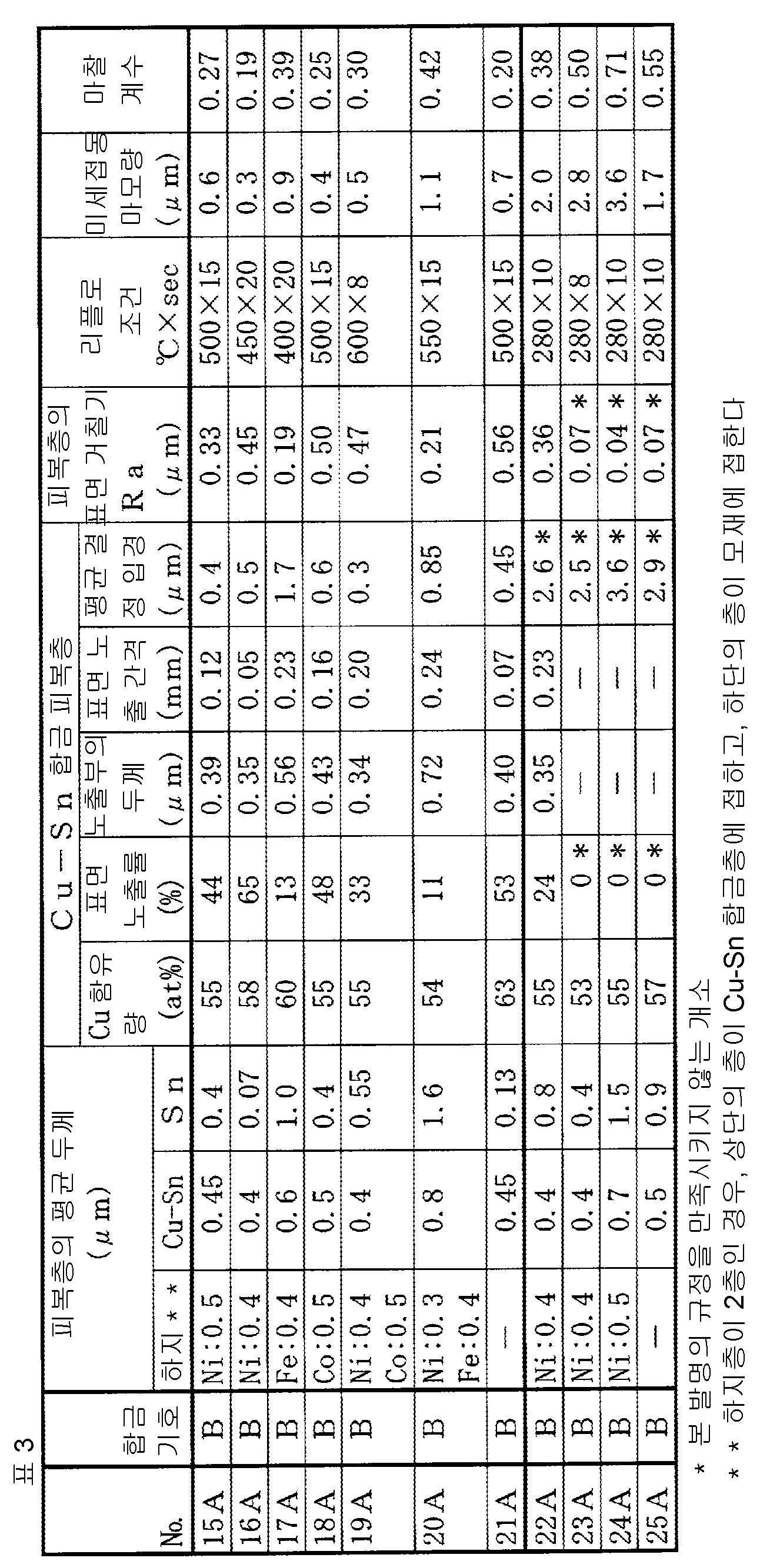
얻어진 시험재에 대하여, 실시예 1과 마찬가지의 측정 및 시험을 행했다. 그 밖에, 얻어진 시험재에 대하여, 하기 요령으로 Co 피복층 및 Fe 피복층의 평균 두께의 측정, 및 마찰 계수의 측정을 행했다. 그 결과를 표 3에 나타낸다. 한편, No. 11∼25의 시험재에 있어서, Cu 도금층은 소멸되어 있었다.The obtained test materials were subjected to the same measurements and tests as in Example 1. In addition, the obtained test materials were measured for the average thickness of the Co coating layer and the Fe coating layer, and the coefficient of friction was measured in the following manner. The results are shown in Table 3. On the other hand, In the test pieces 11 to 25, the Cu plating layer was annihilated.
(Co층의 평균 두께의 측정)(Measurement of average thickness of Co layer)
형광 X선 막후계(세이코인스트루먼츠 주식회사; SFT3200)를 이용하여, 시험재의 Co층의 평균 두께를 산출했다. 측정 조건은, 검량선에 Sn/Co/모재의 2층 검량선을 이용하고, 콜리메이터 지름을 φ0.5mm로 했다. 동일 시험재에 대하여 상이한 3개소를 측정하고, 그의 평균값을 Co 피복층의 평균 두께로 했다.The average thickness of the Co layer of the test material was calculated using a fluorescent X-ray film thickness meter (Seiko Instruments Inc., SFT3200). As the measurement conditions, a two-layer calibration curve of Sn / Co / base material was used for the calibration curve, and the diameter of the collimator was set to 0.5 mm. Three different portions were measured for the same test material, and the average value thereof was taken as the average thickness of the Co coating layer.
(Fe층의 평균 두께의 측정)(Measurement of average thickness of Fe layer)
형광 X선 막후계(세이코인스트루먼츠 주식회사; SFT3200)를 이용하여, 시험재의 Fe층의 평균 두께를 산출했다. 측정 조건은, 검량선에 Sn/Fe/모재의 2층 검량선을 이용하고, 콜리메이터 지름을 φ0.5mm로 했다. 동일 시험재에 대하여 상이한 3개소를 측정하고, 그의 평균값을 Fe 피복층의 평균 두께로 했다.The average thickness of the Fe layer of the test material was calculated using a fluorescent X-ray film thickness meter (Seiko Instruments Inc., SFT3200). As the measurement conditions, a two-layer calibration curve of Sn / Fe / base material was used for the calibration curve, and the diameter of the collimator was set to 0.5 mm. Three different portions were measured for the same test material, and the average value thereof was taken as the average thickness of the Fe coating layer.
(마찰 계수의 측정)(Measurement of Friction Coefficient)
감합형 접속 부품에 있어서의 전기 접점의 인덴트부의 형상을 모의하여, 도 3에 나타내는 바와 같은 장치를 이용하여 측정했다. 우선, No. 15A∼25A의 각 시험재로부터 잘라낸 판재의 수컷형 시험편(6)을 수평인 대(7)에 고정하고, 그 위에 No. 23A의 시험재(표면에 Cu-Sn 합금층이 노출되지 않는다)로부터 잘라낸 반구 가공재(외경을 φ1.8mm로 했다)의 암컷형 시험편(8)을 두어 표면끼리를 접촉시켰다. 계속해서, 암컷형 시험편(8)에 3.0N의 하중(추(9))을 걸어 수컷형 시험편(6)을 누르고, 가로형 하중 측정기(아이코엔지니어링 주식회사; Model-2152)를 이용하여, 수컷형 시험편(6)을 수평 방향으로 인장하고(접동 속도를 80mm/min로 했다), 접동 거리 5mm까지의 최대 마찰력 F(단위: N)를 측정했다. 마찰 계수를 하기 식(1)에 의해 구했다. 한편, 10은 로드 셀, 화살표는 접동 방향이고, 접동 방향은 압연 방향에 수직인 방향으로 했다. 한편, 수컷형 시험편(1), 암컷형 시험편(3) 모두 길이 방향이 압연 방향과 직행하도록 채취하고 있다.The shape of the indent portion of the electrical contact in the interdigitated connection part was simulated and measured using an apparatus as shown in Fig. First, The male
마찰 계수=F/3.0 ···(1)Friction coefficient = F / 3.0 (1)
동일 시험재로부터, 수컷형 시험편(1)과 암컷형 시험편(3)을 3개씩 잘라내어 3회 시험을 행하고, 3개의 측정 결과의 최대값을 그 시험재의 마찰 계수로 했다.Three male test pieces (1) and three female test pieces (3) were cut out from the same test piece and subjected to trials three times. The maximum value of the three test results was regarded as the coefficient of friction of the test material.
표 3에 나타내는 바와 같이, No. 15A∼21은, 각 피복층의 평균 두께, Cu-Sn 합금 피복층의 Cu 함유량, 재료 표면 거칠기, Cu-Sn 합금 피복층의 재료 표면 노출 면적률, 재료 표면에 노출되는 Cu-Sn 합금 피복층의 두께, Cu-Sn 합금 피복층의 평균 재료 표면 노출 간격에 대하여, 본 발명의 규정을 만족시킨다. 이 중, 리플로 처리 온도가 낮아 승온 속도가 작았던 No. 22A는 Cu-Sn 합금 피복층 표면의 평균 결정 입경이 2.6μm로, 본 발명의 규정을 만족시키지 않는다. 이에 비하여, 리플로 처리 온도가 높아 승온 속도가 컸던 No. 15A∼21A는 Cu-Sn 합금 피복층 표면의 평균 결정 입경이 본 발명의 규정을 만족시킨다. No. 15A∼21A는 모두 미세접동 마모량이 No. 22A보다 적다. 한편, No. 22A도 Cu-Sn 합금 피복층의 재료 표면 노출 면적률이 0(Cu-Sn 합금 피복층이 최표면에 노출되어 있지 않다)인 No. 23A∼25A에 비하면, 미세접동 후의 마모량이 적다.As shown in Table 3, 15A to 21 show the average thicknesses of the respective coating layers, the Cu content of the Cu-Sn alloy coating layer, the surface roughness of the material, the exposed surface area of the material of the Cu-Sn alloy coating layer, the thickness of the Cu- -Sn alloy coating layer, the present invention satisfies the requirements of the present invention. Among them, the No. 1 in which the rate of temperature rise was low due to the low reflow processing temperature. 22A had an average crystal grain size of 2.6 mu m on the surface of the Cu-Sn alloy coating layer and did not satisfy the requirements of the present invention. On the other hand, when the temperature of the reflow process was high and the rate of temperature increase was large, 15A to 21A, the average crystal grain size of the surface of the Cu-Sn alloy coating layer satisfies the requirements of the present invention. No. 15A to 21A all have a fine sliding wear amount of no. 22A. On the other hand, 22A shows that the material surface exposed area ratio of the Cu-Sn alloy coating layer is 0 (the Cu-Sn alloy coating layer is not exposed on the outermost surface). 23A to 25A, the abrasion amount after fine sliding is small.
또한, Sn 피복층의 평균 두께가 0.2μm 미만인 No. 16A, 21A는 마찰 계수가 극히 낮다.Further, when the Sn-coated layer has an average thickness of less than 0.2 占 퐉, 16A and 21A have an extremely low friction coefficient.
[실시예 3A][Example 3A]
실시예 2A에서 제작한 발명예 No. 15A에 대하여, 리플로 처리 후에 다양한 두께로 전기 광택 Sn 도금을 실시하여, No. 26A∼29A의 시험재를 얻었다. Sn 도금층의 평균 두께는 하기 요령으로 측정하고, 그 결과를 표 4에 나타낸다. 얻어진 시험재에 대하여, 실시예 2A와 마찬가지의 미세접동 마모 시험과 마찰 계수의 측정 시험 외, 땜납 젖음성의 평가 시험을 행했다. 그 결과를 표 4에 나타낸다.Example No. 2 produced in Example 2A. 15A was subjected to electroless Sn plating with various thicknesses after the reflow treatment. Test materials of 26A to 29A were obtained. The average thickness of the Sn-plated layer was measured in the following manner, and the results are shown in Table 4. The resulting test assembly was subjected to the evaluation test of the solder wettability in addition to the fine sliding wear test and the friction coefficient measurement test similar to those in Example 2A. The results are shown in Table 4.

(Sn 도금층의 평균 두께 측정 방법)(Method for Measuring Average Thickness of Sn Plating Layer)
No. 26A∼29A의 시험재에 대하여, 실시예 1A에 기재한 측정 방법으로, Sn 피복층 전체(전기 광택 Sn 도금에 의한 Sn 도금층을 포함한다)의 평균 두께를 구했다. Sn 피복층 전체의 평균 두께로부터, No. 15A의 Sn 피복층(전기 광택 Sn 도금에 의한 Sn 도금층을 포함하지 않는다)의 평균 두께를 빼는 것에 의해, Sn 도금층의 평균 두께를 산출했다.No. For the test materials of 26A to 29A, the average thickness of the entire Sn coating layer (including the Sn plating layer by electropolishing Sn plating) was determined by the measuring method described in Example 1A. From the average thickness of the entire Sn coating layer, The average thickness of the Sn plating layer was calculated by subtracting the average thickness of the Sn coating layer of 15A (containing no Sn plating layer by electropolishing Sn plating).
(땜납 젖음 시험)(Solder wet test)
각각의 시험재 No. 15A, 26A∼29A로부터 잘라낸 시험편에 대하여, 비활성 플럭스를 1초간 침지 도포한 후, 메니스코그래프법으로 제로 크로스 타임과 최대 젖음 응력을 측정했다. 땜납 조성은 Sn-3.0Ag-0.5Cu로 해서, 시험편을 255℃의 땜납에 침지하고, 침지 조건은 침지 속도를 25mm/sec, 침지 깊이를 12mm, 침지 시간을 5.0sec로 했다. 땜납 젖음성은 제로 크로스 타임≤2.0sec, 최대 젖음 응력≥5mN을 기준으로 해서, 모든 기준을 만족시키는 것을 ○, 어느 한쪽만 만족시키는 것을 △, 어느 기준도 만족시키지 않는 것을 ×로 평가했다.Each test piece No. 15A, and 26A to 29A, an inert flux was immersed for 1 second, and then zero cross time and maximum wetting stress were measured by a meniscograph method. The solder composition was Sn-3.0Ag-0.5Cu, and the test piece was immersed in solder at 255 DEG C, and the immersion condition was set to 25mm / sec, the immersion depth was 12mm, and the immersion time was 5.0sec. The solder wettability was evaluated as satisfying all the criteria on the basis of the zero cross time? 2.0 sec and the maximum wetting stress? 5 mN as?, Satisfying either one as?, And not satisfying any criterion as?
표 4에 나타내는 바와 같이, No. 26A∼29A는, 최표면에 Sn 도금층을 갖고 있기 때문에, No. 15A에 비해 땜납 젖음성이 양호하다. 그 중에서도, No. 26A∼28A는 최표면의 Sn 도금층의 평균 두께가 본 발명의 규정을 만족시키고 있어, 낮은 마찰 계수와 땜납 젖음성을 겸비하고, 미세접동 마모량이 적다. 한편, No. 29A는 땜납 젖음성은 양호하지만, 마찰 계수가 커졌다.As shown in Table 4, 26A to 29A have Sn plating layers on their outermost surfaces. Solder wettability is better than 15A. Among them, No. 26A to 28A, since the average thickness of the Sn-plated layer on the outermost surface satisfies the requirements of the present invention, it has both a low friction coefficient and a low solder wettability and a small amount of wear on the sliding surface. On the other hand, 29A had a good solder wettability but a large coefficient of friction.
<시험 B><Test B>
(실시예 1B)(Example 1B)
표 5에 나타내는 조성을 갖는 구리 합금 주괴를 900∼950℃ 도달 후 2시간 유지하여 열간 압연하고, 750℃ 이상에서 물에 담금질했다. 그 후, 냉간 압연, 소둔, 냉간 압연을 행하는 것에 의해, 표 5에 나타내는 기계적 성질 및 도전율을 갖는 판 두께 0.25mm의 구리 합금판 A∼D를 제작했다. 이들 판재는, 기계적인 방법(2회째의 압연에서 조면화된 롤로 압연 또는 2회째의 냉연 후의 연마)으로 표면 조면화 처리를 행하거나(No. 1B∼11B), 또는 표면 조면화 처리를 행하지 않고(No. 12B∼14B), 다양한 표면 거칠기를 갖는 구리 합금 모재로 마무리했다. 이 Cu-Fe-P 합금 모재 A∼D에 Ni 도금을 행하고(No. 6B, 7B, 14B는 행하지 않고), 추가로 다양한 두께의 Cu 도금 및 Sn 도금을 실시한 후, 리플로 처리 노의 분위기 온도를 조정하고, 표 6에 나타내는 여러 가지의 조건(온도×시간)에서 리플로 처리를 행하는 것에 의해 시험재를 얻었다. 리플로 처리 온도로의 승온 속도는, No. 1B∼10B에서는 15℃/초 이상, No. 11B∼14B에서는 10℃/초 정도였다.The ingot of the copper alloy having the composition shown in Table 5 was maintained at 900 to 950 캜 for 2 hours, hot rolled, and quenched in water at 750 캜 or higher. Thereafter, cold-rolling, annealing, and cold rolling were carried out to produce copper alloy sheets A to D having a thickness of 0.25 mm and having mechanical properties and electrical conductivity shown in Table 5. [ These plates are subjected to a surface roughening treatment (No. 1B to 11B) by a mechanical method (rolling with a roughened roll at the second rolling or polishing after the second cold rolling), or without surface roughening (No. 12B to No. 14B) and finished with a copper alloy base material having various surface roughnesses. The Cu-Fe-P alloy base materials A to D were subjected to Ni plating (No. 6B, 7B, and 14B were not performed) and further Cu plating and Sn plating were performed in various thicknesses. And a reflow process was performed under various conditions (temperature x time) shown in Table 6 to obtain a test material. The rate of temperature rise to the reflow processing temperature is as follows. 15 ° C / second or more for 1B to 10B, And about 10 DEG C / second for 11B to 14B.
한편, Cu-Fe-P 합금판의 기계적 성질 및 도전율은 도금 전의 판재로부터 채취한 시험재에 대하여 실시예 1A와 동일한 요령으로 측정했다. 단, 응력 완화율은 시험편의 가열 온도를 150℃로 했다.On the other hand, the mechanical properties and the electric conductivity of the Cu-Fe-P alloy sheet were measured in the same manner as in Example 1A with respect to the test material collected from the plate material before plating. The stress relaxation rate was set at 150 캜 for the heating temperature of the test piece.


얻어진 시험재에 대하여, 각 피복층의 평균 두께, Cu-Sn 합금 피복층의 Cu 함유량, Cu-Sn 합금 피복층의 재료 표면 노출 면적률, 재료 표면에 노출되는 Cu-Sn 합금 피복층의 두께, Cu-Sn 합금 피복층의 평균 재료 표면 노출 간격, Cu-Sn 합금 피복층 표면의 평균 결정 입경 및 재료 표면 거칠기를 하기 요령으로 측정했다. 그 결과를 표 6에 나타낸다. 한편, No. 1B∼14B의 시험재는 리플로 처리에 의해 Cu 도금층은 소멸되어, Cu 피복층이 존재하지 않는다.The average thickness of each coating layer, the Cu content of the Cu-Sn alloy coating layer, the exposed surface area of the material of the Cu-Sn alloy coating layer, the thickness of the Cu-Sn alloy coating layer exposed on the surface of the material, The mean material surface exposure interval of the coating layer, the average crystal grain size on the surface of the Cu-Sn alloy coating layer, and the surface roughness of the material were measured in the following manner. The results are shown in Table 6. On the other hand, 1B to 14B, the Cu plating layer is extinguished by the reflow treatment, and the Cu coating layer is not present.
하기 측정 방법은 Cu-Sn 합금 피복층 표면의 평균 결정 입경의 측정 방법을 제외하고, 특허문헌 2에 기재된 방법을 모방했다.The following measurement method imitated the method described in
Ni 피복층의 평균 두께 측정 방법, Cu-Sn 합금 피복층의 평균 두께 측정 방법, Sn 피복층의 평균 두께 측정 방법, 표면 거칠기 측정 방법, Cu-Sn 합금 피복층의 재료 표면 노출 면적률 측정 방법, Cu-Sn 합금 피복층의 평균 재료 표면 노출 간격 측정 방법, 재료 표면에 노출되는 Cu-Sn 합금 피복층의 두께 측정 방법, Cu-Sn 합금 피복층 표면의 평균 결정 입경 측정 방법은, 실시예 1A와 동일한 방법으로 측정했다. 한편, 시험재 No. 4B의 표면 조직 사진을 도 4에 나타낸다.A method of measuring the average thickness of the Ni-coated layer, a method of measuring the average thickness of the Cu-Sn alloy coated layer, a method of measuring the average thickness of the Sn coated layer, a method of measuring the surface roughness, a method of measuring the exposed surface area of the material of the Cu- A method for measuring the average material surface exposure interval of the coating layer, a method for measuring the thickness of the Cu-Sn alloy coating layer exposed on the surface of the material, and an average crystal grain size measurement method for the surface of the Cu-Sn alloy coating layer were measured in the same manner as in Example 1A. On the other hand, Fig. 4 shows a photograph of the surface texture of 4B.
또한, 얻어진 시험재에 대하여, 실시예 1A와 동일한 방법으로 미세접동 마모 시험을 행하고, 미세접동 후의 마모량을 측정했다. 그 결과를 동일하게 표 6에 나타낸다.The obtained test piece was subjected to a fine sliding wear test in the same manner as in Example 1A, and the amount of wear after fine sliding was measured. The results are also shown in Table 6.
표 6에 나타내는 바와 같이, No. 1B∼10B는 각 피복층의 평균 두께, Cu-Sn 합금 피복층의 Cu 함유량, 재료 표면 거칠기, Cu-Sn 합금 피복층의 재료 표면 노출 면적률, 재료 표면에 노출되는 Cu-Sn 합금 피복층의 두께, Cu-Sn 합금 피복층의 평균 재료 표면 노출 간격에 대하여, 본 발명의 규정을 만족시킨다. 이 중, 리플로 처리 온도가 낮아 승온 속도가 작았던 No. 11B는 Cu-Sn 합금 피복층 표면의 평균 결정 입경이 3.5μm로, 본 발명의 규정을 만족시키지 않는다. 이에 비하여, 리플로 처리 온도가 높아 승온 속도가 컸던 No. 1B∼10B는 Cu-Sn 합금 피복층 표면의 평균 결정 입경이 본 발명의 규정을 만족시킨다.As shown in Table 6, 1B to 10B are graphs showing the average thicknesses of the respective coating layers, the Cu content of the Cu-Sn alloy coating layer, the material surface roughness, the exposed surface area of the material of the Cu-Sn alloy coating layer, the thickness of the Cu- Sn alloy coating layer of the present invention satisfies the requirements of the present invention. Among them, the No. 1 in which the rate of temperature rise was low due to the low reflow processing temperature. 11B have an average crystal grain size of 3.5 mu m on the surface of the Cu-Sn alloy coating layer and do not satisfy the requirements of the present invention. On the other hand, when the temperature of the reflow process was high and the rate of temperature increase was large, 1B to 10B, the average crystal grain size of the surface of the Cu-Sn alloy coating layer satisfies the requirements of the present invention.
No. 1B∼10B는 모두 미세접동 마모량이 No. 11B보다 적고, 특히 모재가 동일한 재질이고 피복층 구조가 유사한 No. 3B와 No. 11B를 비교하면, No. 3B의 미세접동 마모량은 No. 11B의 마모량의 38%로 감소되어 있다.No. 1B to 10B show that the fine sliding wear amount is no. 11B, and particularly the base material is the same material and the coating layer structure is similar. 3B and No. 3. 11B. The wear amount of fine sliding of 3B was as follows. 11B is reduced to 38% of the wear amount.
한편, No. 11B도 Cu-Sn 합금 피복층의 재료 표면 노출 면적률이 0(Cu-Sn 합금 피복층이 최표면에 노출되어 있지 않다)인 No. 12B∼14B에 비하면, 미세접동 마모량이 적다.On the other hand, 11B also shows that the material surface exposed area ratio of the Cu-Sn alloy coating layer is 0 (the Cu-Sn alloy coating layer is not exposed on the outermost surface). 12B to 14B, the amount of fine sliding wear is small.
(실시예 2B)(Example 2B)
표 5의 합금 기호 B의 Cu-Fe-P 합금 주괴에 대하여, 실시예 1B와 마찬가지인 방법으로, 기계적인 방법(압연 또는 연마)으로 표면 조면화 처리를 행하거나(No. 15B∼22B), 또는 표면 조면화 처리를 행하지 않고(No. 23B∼25B), 다양한 표면 거칠기를 갖는 구리 합금 모재로 마무리했다(0.2% 내력: LD 533∼544MPa, TD 539∼551MPa, 도전율: 78∼82% IACS, 응력 완화율: LD 31∼32%, TD 43∼14%). 이 구리 합금 모재에 하지 도금(Ni, Co, Fe 중 1종 또는 2종)을 행하고(No. 21B, 25B는 행하지 않고), 추가로 다양한 두께의 Cu 도금 및 Sn 도금을 실시했다. 이어서, 리플로 처리 노의 분위기 온도를 조정하고, 표 7에 나타내는 여러 가지의 조건(온도×시간)에서 리플로 처리를 행하는 것에 의해 시험재를 얻었다. 리플로 처리 온도로의 승온 속도는, No. 15B∼21B에서는 15℃/초 이상, No. 22B∼25B에서는 10℃/초 정도였다.The surface roughening treatment (No. 15B to 22B) was conducted by a mechanical method (rolling or polishing) in the same manner as in Example 1B for the Cu-Fe-P alloy ingot of alloy symbol B in Table 5, (0.2% strength: LD 533 to 544 MPa, TD 539 to 551 MPa, conductivity: 78 to 82% IACS, stress (tensile strength), and the like) without performing the surface roughening treatment (No. 23B to 25B) Relaxation rate: LD 31 to 32%, TD 43 to 14%). Cu plating and Sn plating of various thicknesses were further performed on this copper alloy base material (one or two kinds of Ni, Co, and Fe) were performed (No. 21B and 25B were not performed). Subsequently, the atmosphere temperature of the reflow processing furnace was adjusted, and the reflow treatment was carried out under various conditions (temperature x time) shown in Table 7 to obtain a test material. The rate of temperature rise to the reflow processing temperature is as follows. 15 ° C / second or more for 15B to 21B; And about 10 DEG C / second for 22B to 25B.

얻어진 시험재에 대하여, 실시예 1B와 마찬가지의 측정 및 시험을 행했다. 그 밖에, 얻어진 시험재에 대하여, 실시예 2A와 동일한 방법으로 Co 피복층 및 Fe 피복층의 평균 두께의 측정, 및 마찰 계수의 측정을 행했다. 그 결과를 표 7에 나타낸다. 한편, No. 15B∼25B의 시험재에 있어서, Cu 도금층은 소멸되어 있었다.The obtained test materials were subjected to the same measurement and tests as in Example 1B. In addition to the test materials thus obtained, the average thickness of the Co coating layer and the Fe coating layer and the coefficient of friction were measured in the same manner as in Example 2A. The results are shown in Table 7. On the other hand, In the test materials of 15B to 25B, the Cu plating layer was annihilated.
표 7에 나타내는 바와 같이, No. 15B∼21B는, 각 피복층의 평균 두께, Cu-Sn 합금 피복층의 Cu 함유량, 재료 표면 거칠기, Cu-Sn 합금 피복층의 재료 표면 노출 면적률, 재료 표면에 노출되는 Cu-Sn 합금 피복층의 두께, Cu-Sn 합금 피복층의 평균 재료 표면 노출 간격에 대하여, 본 발명의 규정을 만족시킨다. 이 중, 리플로 처리 온도가 낮아 승온 속도가 작았던 No. 22B는 Cu-Sn 합금 피복층 표면의 평균 결정 입경이 2.7μm로, 본 발명의 규정을 만족시키지 않는다. 이에 비하여, 리플로 처리 온도가 높아 승온 속도가 컸던 No. 15B∼21B는 Cu-Sn 합금 피복층 표면의 평균 결정 입경이 본 발명의 규정을 만족시킨다. No. 15B∼21B는 모두 미세접동 마모량이 No. 22B보다 적다. 한편, No. 22B도 Cu-Sn 합금 피복층의 재료 표면 노출 면적률이 0(Cu-Sn 합금 피복층이 최표면에 노출되어 있지 않다)인 No. 23B∼25B에 비하면, 미세접동 후의 마모량이 적다.As shown in Table 7, 15B to 21B are graphs showing the average thicknesses of the respective coating layers, the Cu content of the Cu-Sn alloy coating layer, the material surface roughness, the exposed surface area of the material of the Cu-Sn alloy coating layer, the thickness of the Cu- -Sn alloy coating layer, the present invention satisfies the requirements of the present invention. Among them, the No. 1 in which the rate of temperature rise was low due to the low reflow processing temperature. 22B have an average crystal grain size of 2.7 mu m on the surface of the Cu-Sn alloy coating layer and do not satisfy the requirements of the present invention. On the other hand, when the temperature of the reflow process was high and the rate of temperature increase was large, 15B to 21B, the average crystal grain size on the surface of the Cu-Sn alloy coating layer satisfies the requirements of the present invention. No. 15B to 21B are all shown in Fig. 22B. On the other hand, 22B shows that the material surface exposed area ratio of the Cu-Sn alloy coating layer is 0 (the Cu-Sn alloy coating layer is not exposed on the outermost surface). 23B to 25B, the abrasion amount after fine sliding is small.
또한, Sn 피복층의 평균 두께가 0.2μm 미만인 No. 16B, 21B는 마찰 계수가 극히 낮다.Further, when the Sn-coated layer has an average thickness of less than 0.2 占 퐉, 16B, and 21B have extremely low friction coefficients.
(실시예 3B)(Example 3B)
실시예 2B에서 제작한 발명예 No. 15B에 대하여, 리플로 처리 후에 다양한 두께로 전기 광택 Sn 도금을 실시하여, No. 26B∼29B의 시험재를 얻었다. Sn 도금층의 평균 두께는 하기 요령으로 측정하고, 그 결과를 표 8에 나타낸다. 얻어진 시험재에 대하여, 실시예 2B와 마찬가지의 미세접동 마모 시험과 마찰 계수의 측정 시험 외, 땜납 젖음성의 평가 시험을 행했다. 그 결과를 표 8에 나타낸다.Example No. 2 produced in Example 2B. 15B were subjected to electroless Sn plating in various thicknesses after the reflow treatment. Test materials of 26B to 29B were obtained. The average thickness of the Sn-plated layer was measured in the following manner, and the results are shown in Table 8. The resulting test assembly was subjected to evaluation tests of solder wettability in addition to the fine sliding wear test and the friction coefficient measurement test as in Example 2B. The results are shown in Table 8.

(Sn 도금층의 평균 두께 측정 방법)(Method for Measuring Average Thickness of Sn Plating Layer)
No. 26B∼29B의 시험재에 대하여, 실시예 1B에 기재한 측정 방법으로, Sn 피복층 전체(전기 광택 Sn 도금에 의한 Sn 도금층을 포함한다)의 평균 두께를 구했다. Sn 피복층 전체의 평균 두께로부터, No. 15B의 Sn 피복층(전기 광택 Sn 도금에 의한 Sn 도금층을 포함하지 않는다)의 평균 두께를 빼는 것에 의해, Sn 도금층의 평균 두께를 산출했다.No. 26B to 29B, the average thickness of the entire Sn coating layer (including Sn plating layer by electropolished Sn plating) was determined by the measuring method described in Example 1B. From the average thickness of the entire Sn coating layer, The average thickness of the Sn plating layer was calculated by subtracting the average thickness of the Sn coating layer (not including the Sn plating layer by electropolishing Sn plating) of 15B.
(땜납 젖음 시험)(Solder wet test)
각각의 시험재 No. 15B, 26B∼29B로부터 잘라낸 시험편에 대하여, 비활성 플럭스를 1초간 침지 도포한 후, 메니스코그래프법으로 제로 크로스 타임과 최대 젖음 응력을 측정했다. 땜납 조성은 Sn-3.0Ag-0.5Cu로 해서, 시험편을 255℃의 땜납에 침지하고, 침지 조건은 침지 속도를 25mm/sec, 침지 깊이를 12mm, 침지 시간을 5.0sec로 했다. 땜납 젖음성은 제로 크로스 타임≤2.0sec, 최대 젖음 응력≥5mN을 기준으로 해서, 모든 기준을 만족시키는 것을 ○, 어느 한쪽만 만족시키는 것을 △, 어느 기준도 만족시키지 않는 것을 ×로 평가했다.Each test piece No. 15B, and 26B to 29B, an inert flux was immersed for 1 second, and then zero cross time and maximum wetting stress were measured by a meniscograph method. The solder composition was Sn-3.0Ag-0.5Cu, and the test piece was immersed in solder at 255 DEG C, and the immersion condition was set to 25mm / sec, the immersion depth was 12mm, and the immersion time was 5.0sec. The solder wettability was evaluated as satisfying all the criteria on the basis of the zero cross time ≤2.0 sec and the maximum wetting stress ≥5 mN as ◯, satisfying only one of them as △, and not satisfying any criterion as ×.
표 8에 나타내는 바와 같이, No. 26B∼29B는 최표면에 Sn 도금층을 갖고 있기 때문에, No. 15B에 비해 땜납 젖음성이 양호하다. 그 중에서도, No. 26B∼28B는 최표면의 Sn 도금층의 평균 두께가 본 발명의 규정을 만족시키고 있어, 낮은 마찰 계수와 땜납 젖음성을 겸비하고, 미세접동 마모량이 적다. 한편, No. 29B는 땜납 젖음성은 양호하지만, 마찰 계수가 커졌다.As shown in Table 8, 26B to 29B have Sn plating layers on their outermost surfaces. 15B, the solder wettability is good. Among them, No. 26B to 28B, the average thickness of the Sn-plated layer on the outermost surface satisfies the requirements of the present invention, and has a low friction coefficient and solder wettability, and the amount of fine sliding wear is small. On the other hand, 29B exhibited good solder wettability but had a large coefficient of friction.
<시험 C><Test C>
[실시예 1C][Example 1C]
표 9에 나타내는 조성을 갖는 구리 합금 주괴를 700∼850℃ 도달 후 2시간 유지하여 열간 압연하고, 열간 압연 종료 후 물에 담금질했다. 그 후, 냉간 압연, 소둔, 냉간 압연, 변형 교정 소둔(재결정하지 않는 조건)을 행하는 것에 의해, 표 9에 나타내는 기계적 성질 및 도전율을 갖는 판 두께 0.25mm의 구리 합금판 A∼D를 제작했다. 이들 판재는 기계적인 방법(2회째의 압연에서 조면화된 롤로 압연 또는 2회째의 냉연 후의 연마)으로 표면 조면화 처리를 행하거나(No. 1C∼11C), 또는 표면 조면화 처리를 행하지 않고(No. 12C∼14C), 다양한 표면 거칠기를 갖는 구리 합금 모재로 마무리했다. 이 Cu-Zn 합금 모재 A∼D에 Ni 도금을 행하고(No. 6C, 7C, 14C는 행하지 않고), 추가로 다양한 두께의 Cu 도금 및 Sn 도금을 실시한 후, 리플로 처리 노의 분위기 온도를 조정하고, 표 10에 나타내는 여러 가지의 조건(온도×시간)에서 리플로 처리를 행하는 것에 의해 시험재를 얻었다. 리플로 처리 온도로의 승온 속도는, No. 1C∼10C에서는 15℃/초 이상, No. 11C∼14C에서는 10℃/초 정도였다.The ingot of the copper alloy having the composition shown in Table 9 was maintained at 700 to 850 캜 for 2 hours and then hot-rolled, and quenched in water after completion of the hot-rolling. Thereafter, cold-rolled, annealed, cold rolled, and strain-correcting annealing (conditions without recrystallization) were carried out to produce copper alloy sheets A to D having a thickness of 0.25 mm and mechanical properties shown in Table 9 and electrical conductivity. These plates are subjected to a surface roughening treatment (No. 1C to 11C) or a surface roughening treatment (No. 1C to No. 11C) by a mechanical method (rolling with a roughened roll at the second rolling or polishing after the second cold rolling) No. 12C to 14C) and finished with a copper alloy base material having various surface roughnesses. The Cu-Zn alloy base materials A to D were subjected to Ni plating (No. 6C, 7C, and 14C were not performed), Cu plating and Sn plating of various thicknesses were further performed, and then the atmosphere temperature of the reflow processing furnace was adjusted , And subjected to a reflow treatment under various conditions (temperature x time) shown in Table 10 to obtain test materials. The rate of temperature rise to the reflow processing temperature is as follows. 15 ° C / sec or more for 1C to 10C, And about 10 DEG C / sec for 11C to 14C.
도금 전의 판재로부터 채취한 시험재에 대하여 실시예 1A와 동일한 요령으로 기계적 성질, 응력 완화율 및 도전율을 측정했다. 단, 0.2% 내력 및 신도는 길이 방향이 압연 방향에 평행해지는 방향(LD)으로 채취한 인장 시험편에 의해 측정하고, 응력 완화율은 길이 방향이 LD 방향에 평행해지도록 채취한 시험편을 이용하고, 시험편의 가열 온도를 150℃로 했다.The mechanical properties, the stress relaxation rate and the electrical conductivity were measured in the same manner as in Example 1A with respect to the test material collected from the plate material before plating. However, the 0.2% proof stress and elongation were measured by tensile test specimens taken in a direction (LD) in which the longitudinal direction was parallel to the rolling direction, and the stress relaxation rate was measured using a test specimen obtained in such a manner that the longitudinal direction was parallel to the LD direction, The heating temperature of the test piece was set at 150 캜.
한편, Cu-Zn 합금판의 평균 결정 입경, 및 W 굽힘성은 이하의 요령으로 측정했다.On the other hand, the average crystal grain size and W bendability of the Cu-Zn alloy sheet were measured in the following manner.
평균 결정 입경은, JIS H 0501에 기초해서, Cu-Zn 합금판의 표면에 수직이고 압연 방향에 평행한 단면에 있어서, 절단법(절단 방향은 판 두께 방향)에 의해 측정했다.The average crystal grain size was measured on the basis of JIS H 0501 on a section perpendicular to the surface of the Cu-Zn alloy plate and parallel to the rolling direction by the cutting method (the cutting direction was the thickness direction).
W 굽힘성은 신동협회 표준 JBMA-T307에 규정되는 W 굽힘 시험 방법에 의해 측정했다. 시험편은 길이 방향이 압연 평행 방향이 되도록 채취하여, GW(good way) 굽힘을 행했다.The W bendability was measured by the W bending test method prescribed in Shin Dong Association Standard JBMA-T307. The test specimens were taken in the longitudinal direction in the rolling parallel direction, and GW (good way) bending was performed.


얻어진 시험재에 대하여, 각 피복층의 평균 두께, Cu-Sn 합금 피복층의 Cu 함유량, Cu-Sn 합금 피복층의 재료 표면 노출 면적률, 재료 표면에 노출되는 Cu-Sn 합금 피복층의 두께, Cu-Sn 합금 피복층의 평균 재료 표면 노출 간격, Cu-Sn 합금 피복층 표면의 평균 결정 입경 및 재료 표면 거칠기를 하기 요령으로 측정했다. 그 결과를 표 10에 나타낸다. 한편, No. 1C∼14C의 시험재는 리플로 처리에 의해 Cu 도금층이 소멸되어, Cu 피복층이 존재하지 않는다.The average thickness of each coating layer, the Cu content of the Cu-Sn alloy coating layer, the exposed surface area of the material of the Cu-Sn alloy coating layer, the thickness of the Cu-Sn alloy coating layer exposed on the surface of the material, The mean material surface exposure interval of the coating layer, the average crystal grain size on the surface of the Cu-Sn alloy coating layer, and the surface roughness of the material were measured in the following manner. The results are shown in Table 10. On the other hand, In the test pieces of 1C to 14C, the Cu plating layer is destroyed by the reflow treatment, and the Cu coating layer is not present.
하기 측정 방법은 Cu-Sn 합금 피복층 표면의 평균 결정 입경의 측정 방법을 제외하고, 특허문헌 2에 기재된 방법을 모방했다.The following measurement method imitated the method described in
Ni 피복층의 평균 두께 측정 방법, Cu-Sn 합금 피복층의 평균 두께 측정 방법, Sn 피복층의 평균 두께 측정 방법, 표면 거칠기 측정 방법, Cu-Sn 합금 피복층의 재료 표면 노출 면적률 측정 방법, Cu-Sn 합금 피복층의 평균 재료 표면 노출 간격 측정 방법, 재료 표면에 노출되는 Cu-Sn 합금 피복층의 두께 측정 방법, Cu-Sn 합금 피복층 표면의 평균 결정 입경 측정 방법은 실시예 1A와 동일한 방법으로 측정했다. 한편, 시험재 No. 4B의 표면 조직 사진을 도 4에 나타낸다.A method of measuring the average thickness of the Ni-coated layer, a method of measuring the average thickness of the Cu-Sn alloy coated layer, a method of measuring the average thickness of the Sn coated layer, a method of measuring the surface roughness, a method of measuring the exposed surface area of the material of the Cu- A method of measuring the average material surface exposure interval of the coating layer, a method of measuring the thickness of the Cu-Sn alloy coating layer exposed on the material surface, and an average crystal grain size measurement method of the surface of the Cu-Sn alloy coating layer were measured in the same manner as in Example 1A. On the other hand, Fig. 4 shows a photograph of the surface texture of 4B.
표 10에 나타내는 바와 같이, No. 1C∼11C는, 각 피복층의 평균 두께, Cu-Sn 합금 피복층의 Cu 함유량, 재료 표면 거칠기, Cu-Sn 합금 피복층의 재료 표면 노출 면적률, 재료 표면에 노출되는 Cu-Sn 합금 피복층의 두께, Cu-Sn 합금 피복층의 평균 재료 표면 노출 간격에 대하여, 본 발명의 규정을 만족시킨다. 이 중, 리플로 처리 온도가 낮아 승온 속도가 작았던 No. 11C는 Cu-Sn 합금 피복층 표면의 평균 결정 입경이 3.20μm로, 본 발명의 규정을 만족시키지 않는다. 이에 비하여, 리플로 처리 온도가 높아 승온 속도가 컸던 No. 1C∼10C는 Cu-Sn 합금 피복층 표면의 평균 결정 입경이 본 발명의 규정을 만족시킨다. No. 1C∼10C는 모두 미세접동 마모량이 No. 11C보다 적고, 특히 모재가 동일한 재질이고 피복층 구조가 유사한 No. 3C와 No. 11C를 비교하면, No. 3C의 미세접동 마모량은 No. 7C의 마모량의 47%로 감소되어 있다.As shown in Table 10, 1C to 11C are graphs showing the average thicknesses of the respective coating layers, the Cu content of the Cu-Sn alloy coating layer, the material surface roughness, the exposed surface area of the material of the Cu-Sn alloy coating layer, the thickness of the Cu- -Sn alloy coating layer, the present invention satisfies the requirements of the present invention. Among them, the No. 1 in which the rate of temperature rise was low due to the low reflow processing temperature. 11C have an average crystal grain size of 3.20 mu m on the surface of the Cu-Sn alloy coating layer, and do not satisfy the requirements of the present invention. On the other hand, when the temperature of the reflow process was high and the rate of temperature increase was large, 1C to 10C, the average crystal grain size of the surface of the Cu-Sn alloy coating layer satisfies the requirements of the present invention. No. 1C to 10C show that the fine sliding wear amount is no. 11C, and particularly, the base material is the same material and the coating layer structure is similar. 3C and No. 11C. The wear amount of fine sliding of 3C was as follows. 7C is reduced to 47% of the wear amount.
한편, No. 11C도 Cu-Sn 합금 피복층의 재료 표면 노출 면적률이 0(Cu-Sn 합금 피복층이 최표면에 노출되어 있지 않다)인 No. 12C∼14C에 비하면, 미세접동 마모량이 적다.On the other hand, 11C also shows that the material surface exposed area ratio of the Cu-Sn alloy coating layer is 0 (the Cu-Sn alloy coating layer is not exposed on the outermost surface). 12C to 14C, the amount of fine sliding wear is small.
[실시예 2C][Example 2C]
표 9의 합금 기호 B의 Cu-Zn 합금 주괴에 대하여, 실시예 1C와 마찬가지인 방법으로, 기계적인 방법(압연 또는 연마)으로 표면 조면화 처리를 행하거나(No. 15C∼22C), 또는 표면 조면화 처리를 행하지 않고(No. 23C∼25C), 다양한 표면 거칠기를 갖는 구리 합금 모재로 마무리했다(0.2% 내력: 486∼502MPa, 성장: 17∼19%, 도전율: 28% IACS, 응력 완화율: 68∼73%). 이 구리 합금 모재에 하지 도금(Ni, Co, Fe 중 1종 또는 2종)을 행하고(No. 21C, 25C는 행하지 않고), 추가로 다양한 두께의 Cu 도금 및 Sn 도금을 실시했다. 이어서, 리플로 처리 노의 분위기 온도를 조정하고, 표 11에 나타내는 여러 가지의 조건(온도×시간)에서 리플로 처리를 행하는 것에 의해 시험재를 얻었다. 리플로 처리 온도로의 승온 속도는, No. 15C∼21C에서는 15℃/초 이상, No. 22C∼25C에서는 10℃/초속 정도였다.The surface roughening treatment (No. 15C to 22C) was carried out by a mechanical method (rolling or polishing) in the same manner as in Example 1C with respect to the Cu-Zn alloy ingot of alloy symbol B in Table 9, (0.2% proof stress: 486 to 502 MPa, growth: 17 to 19%, conductivity: 28% IACS, stress relaxation rate: 68-73%). Cu plating and Sn plating of various thicknesses were further performed on the copper alloy base material (one or two kinds of Ni, Co, and Fe) were performed (No. 21C and 25C were not performed). Subsequently, the atmosphere temperature of the reflow processing furnace was adjusted, and the reflow treatment was performed under various conditions (temperature x time) shown in Table 11 to obtain test materials. The rate of temperature rise to the reflow processing temperature is as follows. 15 ° C / second or more for 15C to 21C, and 15 ° C / And 22 ° C to 25 ° C, respectively.

얻어진 시험재에 대하여, 실시예 1C와 마찬가지의 측정 및 시험을 행했다. 그 밖에, 얻어진 시험재에 대하여, 실시예 2A와 동일한 방법으로 하기 요령으로 Co 피복층 및 Fe 피복층의 평균 두께의 측정, 및 마찰 계수의 측정을 행했다. 그 결과를 표 11에 나타낸다. 한편, No. 15C∼25C의 시험재에 있어서, Cu 도금층은 소멸되어 있었다.Measurement and test similar to those of Example 1C were conducted on the obtained test materials. In addition to the test materials thus obtained, the average thicknesses of the Co coating layer and the Fe coating layer and the coefficient of friction were measured in the same manner as in Example 2A with the following procedure. The results are shown in Table 11. On the other hand, In the test pieces of 15C to 25C, the Cu plating layer was annihilated.
표 11에 나타내는 바와 같이, No. 15C∼22C는, 각 피복층의 평균 두께, Cu-Sn 합금 피복층의 Cu 함유량, 재료 표면 거칠기, Cu-Sn 합금 피복층의 재료 표면 노출 면적률, 재료 표면에 노출되는 Cu-Sn 합금 피복층의 두께, Cu-Sn 합금 피복층의 평균 재료 표면 노출 간격에 대하여, 본 발명의 규정을 만족시킨다. 이 중, 리플로 처리 온도가 낮아 승온 속도가 작았던 No. 22C는 Cu-Sn 합금 피복층 표면의 평균 결정 입경이 2.7μm로, 본 발명의 규정을 만족시키지 않는다. 이에 비하여, 리플로 처리 온도가 높아 승온 속도가 컸던 No. 15C∼21C는 Cu-Sn 합금 피복층 표면의 평균 결정 입경이 본 발명의 규정을 만족시킨다.As shown in Table 11, 15C to 22C are graphs showing the average thicknesses of the respective coating layers, the Cu content of the Cu-Sn alloy coating layer, the surface roughness of the material, the exposed surface area of the material of the Cu-Sn alloy coating layer, the thickness of the Cu- -Sn alloy coating layer, the present invention satisfies the requirements of the present invention. Among them, the No. 1 in which the rate of temperature rise was low due to the low reflow processing temperature. 22C have an average crystal grain size of 2.7 mu m on the surface of the Cu-Sn alloy coating layer and do not satisfy the requirements of the present invention. On the other hand, when the temperature of the reflow process was high and the rate of temperature increase was large, 15C to 21C, the average crystal grain size of the surface of the Cu-Sn alloy coating layer satisfies the requirements of the present invention.
No. 15C∼21C는 모두 미세접동 마모량이 No. 22C보다 적다. 한편, No. 22C도 Cu-Sn 합금 피복층의 재료 표면 노출 면적률이 0(Cu-Sn 합금 피복층이 최표면에 노출되어 있지 않다)인 No. 23C∼25C에 비하면, 미세접동 후의 마모량이 적다.No. 15C to 21C are all shown in Fig. 22C. On the other hand, 22C shows that the material surface exposed area ratio of the Cu-Sn alloy coating layer is 0 (the Cu-Sn alloy coating layer is not exposed on the outermost surface). 23C to 25C, the abrasion amount after fine sliding is small.
또한, Sn 피복층의 평균 두께가 0.2μm 미만인 No. 16C, 21C는 마찰 계수가 극히 낮다.Further, when the Sn-coated layer has an average thickness of less than 0.2 占 퐉, 16C, and 21C have extremely low friction coefficients.
[실시예 3C][Example 3C]
실시예 2C에서 제작한 발명예 No. 15C에 대하여, 리플로 처리 후에 다양한 두께로 전기 광택 Sn 도금을 실시하여, No. 26C∼29C의 시험재를 얻었다. Sn 도금층의 평균 두께는 하기 요령으로 측정하고, 그 결과를 표 12에 나타낸다. 얻어진 시험재에 대하여, 실시예 2C와 마찬가지의 미세접동 마모 시험과 마찰 계수의 측정 시험 외, 땜납 젖음성의 평가 시험을 행했다. 그 결과를 표 12에 나타낸다.Example No. 2 produced in Example 2C. 15C were subjected to electroless Sn plating with various thicknesses after the reflow treatment. Test materials of 26C to 29C were obtained. The average thickness of the Sn plating layer was measured in the following manner, and the results are shown in Table 12. The resulting test assembly was subjected to the evaluation tests of the solder wettability in addition to the fine sliding wear test and the friction coefficient measurement test as in Example 2C. The results are shown in Table 12.

(Sn 도금층의 평균 두께 측정 방법)(Method for Measuring Average Thickness of Sn Plating Layer)
No. 26C∼29C의 시험재에 대하여, 실시예 1C에 기재한 측정 방법으로, Sn 피복층 전체(전기 광택 Sn 도금에 의한 Sn 도금층을 포함한다)의 평균 두께를 구했다. Sn 피복층 전체의 평균 두께로부터, No. 15C의 Sn 피복층(전기 광택 Sn 도금에 의한 Sn 도금층을 포함하지 않는다)의 평균 두께를 빼는 것에 의해, Sn 도금층의 평균 두께를 산출했다.No. For the test materials of 26C to 29C, the average thickness of the entire Sn coating layer (including the Sn plating layer by electropolished Sn plating) was determined by the measuring method described in Example 1C. From the average thickness of the entire Sn coating layer, The average thickness of the Sn plating layer was calculated by subtracting the average thickness of the Sn coating layer (not including the Sn plating layer by electropolishing Sn plating) of 15C.
(땜납 젖음 시험)(Solder wet test)
각각의 시험재 No. 15C, 26C∼29C로부터 잘라낸 시험편에 대하여, 비활성 플럭스를 1초간 침지 도포한 후, 메니스코그래프법으로 제로 크로스 타임과 최대 젖음 응력을 측정했다. 땜납 조성은 Sn-3.0Ag-0.5Cu로 해서, 시험편을 255℃의 땜납에 침지하고, 침지 조건은 침지 속도를 25mm/sec, 침지 깊이를 12mm, 침지 시간을 5.0sec로 했다. 땜납 젖음성은 제로 크로스 타임≤2.0sec, 최대 젖음 응력≥5mN을 기준으로 해서, 모든 기준을 만족시키는 것을 ○, 어느 한쪽만 만족시키는 것을 △, 어느 기준도 만족시키지 않는 것을 ×로 평가했다.Each test piece No. 15C, and 26C to 29C, an inert flux was immersed for 1 second, and zero cross time and maximum wetting stress were measured by a meniscograph method. The solder composition was Sn-3.0Ag-0.5Cu, and the test piece was immersed in solder at 255 DEG C, and the immersion condition was set to 25mm / sec, the immersion depth was 12mm, and the immersion time was 5.0sec. The solder wettability was evaluated as satisfying all the criteria on the basis of the zero cross time ≤2.0 sec and the maximum wetting stress ≥5 mN as ◯, satisfying only one of them as △, and not satisfying any criterion as ×.
표 12에 나타내는 바와 같이, No. 26C∼30C는 최표면에 Sn 도금층을 갖고 있기 때문에, No. 15C에 비해 땜납 젖음성이 개선되어 있다. 그 중에서도, No. 26C∼28C는 최표면의 Sn 도금층의 평균 두께가 본 발명의 규정을 만족하고 있어, 낮은 마찰 계수와 땜납 젖음성을 겸비하고, 미세접동 마모량이 적다. 한편, No. 29C는 땜납 젖음성은 양호하지만, 마찰 계수가 커졌다.As shown in Table 12, 26C to 30C have Sn plating layers on their outermost surfaces. 15C, the solder wettability is improved. Among them, No. 26C to 28C, the average thickness of the Sn-plated layer on the outermost surface satisfies the requirements of the present invention, has both a low friction coefficient and a good solder wettability, and has a small amount of wear on the sliding surface. On the other hand, 29C had good solder wettability but a large coefficient of friction.
본 발명을 상세히 또한 특정 실시태양을 참조하여 설명했지만, 본 발명의 정신과 범위를 일탈하는 일 없이 다양한 변경이나 수정을 가할 수 있다는 것은 당업자에게 분명하다.While the invention has been described in detail and with reference to specific embodiments thereof, it is evident to those skilled in the art that various changes and modifications can be made without departing from the spirit and scope of the invention.
본 출원은 2014년 8월 25일 출원된 일본 특허출원(특원 2014-170879), 2014년 8월 25일 출원된 일본 특허출원(특원 2014-170956), 2014년 8월 27일 출원된 일본 특허출원(특원 2014-172281)에 기초하는 것이며, 그 내용은 여기에 참조로서 도입된다.The present application is based on Japanese patent application (Specification 2014-170879) filed on August 25, 2014, Japanese Patent Application (Specification 2014-170956) filed on August 25, 2014, Japanese Patent Application filed on August 27, 2014 (Mention 2014-172281), the contents of which are incorporated herein by reference.
본 발명의 접속 부품용 도전 재료는 미세접동 마찰을 지금까지보다도 저감할 수 있어, 자동차 분야나 일반 민생 분야에서 이용되는 단자 등에 유용하다.The conductive material for a connecting part of the present invention can reduce the fine sliding friction more than ever and is useful for a terminal used in the automobile field and the general public sector.
1, 6: 수컷형 시험편
2, 7: 대
3, 8: 암컷형 시험편
4, 9: 추
5: 스텝핑 모터
10: 로드 셀1, 6: male type test piece
2, 7: Stand
3, 8: Female type test piece
4, 9: Chu
5: Stepping motor
10: Load cell
Claims (9)
상기 구리 합금 판조가, 추가로 하기 (A) 및 (B) 중 적어도 하나를 포함하는 것을 특징으로 하는 접속 부품용 도전 재료.
(A) Ti: 0.01∼0.30질량%, Si: 0.01∼0.20질량%로부터 선택되는 1종 또는 2종
(B) Zn: 0.001∼1.0질량%, Sn: 0.001∼0.5질량%, Mg: 0.001∼0.15질량%, Ag: 0.005∼0.50질량%, Fe: 0.005∼0.50질량%, Ni: 0.005∼0.50질량%, Co: 0.005∼0.50질량%, Al: 0.005∼0.10질량%, Mn: 0.005∼0.10질량% 중 1종 이상을 합계로 1.0질량% 이하The method according to claim 1,
Wherein the copper alloy plate assembly further comprises at least one of the following (A) and (B).
(A) 0.01 to 0.30 mass% of Ti, 0.01 to 0.20 mass% of Si,
(B) 0.001 to 1.0 mass% of Zn, 0.001 to 0.5 mass% of Sn, 0.001 to 0.15 mass% of Mg, 0.005 to 0.50 mass% of Ag, 0.005 to 0.50 mass% of Fe, 0.005 to 0.50 mass% of Ni, 0.005 to 0.50 mass% of Co, 0.005 to 0.10 mass% of Al, and 0.005 to 0.10 mass% of Mn in a total amount of 1.0 mass% or less
상기 구리 합금 판조가, 추가로 하기 (C) 및 (D) 중 적어도 하나를 포함하는 것을 특징으로 하는 접속 부품용 도전 재료.
(C) Sn: 0.001∼0.5%, Zn: 0.005∼3.0% 중 1종 또는 2종
(D) Mn, Mg, Ca, Zr, Ag, Cr, Cd, Be, Ti, Si, Co, Ni, Al, Au, Pt로부터 선택된 1종 또는 2종 이상을 합계로 0.001∼0.5질량%The method of claim 3,
Wherein the copper alloy plate assembly further comprises at least one of the following (C) and (D).
(C) one or two of Sn: 0.001 to 0.5%, and Zn: 0.005 to 3.0%
(D) 0.001 to 0.5 mass% in total of one or more species selected from Mn, Mg, Ca, Zr, Ag, Cr, Cd, Be, Ti, Si, Co, Ni, Al, Au,
상기 Cu-Zn 합금 판조가, 추가로 Cr, Ti, Zr, Mg, Sn, Ni, Fe, Co, Mn, Al, P로부터 선택된 1종 또는 2종 이상의 원소를 합계로 0.005∼1질량% 함유하는 것을 특징으로 하는 접속 부품용 도전 재료.6. The method of claim 5,
Wherein the Cu-Zn alloy plate assembly further contains 0.005 to 1 mass% of at least one element selected from the group consisting of Cr, Ti, Zr, Mg, Sn, Ni, Fe, Co, Mn, And a conductive material for a connection part.
상기 모재의 표면과 상기 Cu-Sn 합금 피복층 사이에 추가로 Ni 피복층, Co 피복층, Fe 피복층으로부터 선택되는 1층 또는 2층으로 이루어지는 하지층이 형성되고, 상기 하지층의 평균 두께가, 1층인 경우에는 단독으로, 2층인 경우에는 양층의 합계로, 각각 0.1∼3.0μm인 것을 특징으로 하는 접속 부품용 도전 재료.The method according to claim 1, 3, or 5,
Wherein a base layer composed of one or two layers selected from an Ni coating layer, a Co coating layer and an Fe coating layer is further formed between the surface of the base material and the Cu-Sn alloy coating layer, and when the average thickness of the base layer is one layer Wherein the total thickness of the two layers is 0.1 to 3.0 占 퐉.
상기 하지층과 Cu-Sn 합금 피복층 사이에 추가로 Cu 피복층을 갖는 것을 특징으로 하는 접속 부품용 도전 재료.8. The method of claim 7,
And further has a Cu coating layer between the base layer and the Cu-Sn alloy coating layer.
상기 리플로 처리된 재료 표면에 추가로 평균 두께 0.02∼0.2μm의 Sn 도금층이 형성되어 있는 것을 특징으로 하는 접속 부품용 도전 재료.The method according to claim 1, 3, or 5,
Wherein a Sn plating layer having an average thickness of 0.02 to 0.2 占 퐉 is further formed on the surface of the reflow-processed material.
Applications Claiming Priority (7)
| Application Number | Priority Date | Filing Date | Title |
|---|---|---|---|
| JP2014170879A JP5897082B1 (en) | 2014-08-25 | 2014-08-25 | Conductive material for connecting parts with excellent resistance to fine sliding wear |
| JP2014170956A JP5897083B1 (en) | 2014-08-25 | 2014-08-25 | Conductive material for connecting parts with excellent resistance to fine sliding wear |
| JPJP-P-2014-170956 | 2014-08-25 | ||
| JPJP-P-2014-170879 | 2014-08-25 | ||
| JPJP-P-2014-172281 | 2014-08-27 | ||
| JP2014172281A JP5897084B1 (en) | 2014-08-27 | 2014-08-27 | Conductive material for connecting parts with excellent resistance to fine sliding wear |
| PCT/JP2015/073294 WO2016031654A1 (en) | 2014-08-25 | 2015-08-20 | Conductive material for connection parts which has excellent minute slide wear resistance |
Related Child Applications (2)
| Application Number | Title | Priority Date | Filing Date |
|---|---|---|---|
| KR1020197011834A Division KR102113988B1 (en) | 2014-08-25 | 2015-08-20 | Conductive material for connection parts which has excellent minute slide wear resistance |
| KR1020197011826A Division KR102113989B1 (en) | 2014-08-25 | 2015-08-20 | Conductive material for connection parts which has excellent minute slide wear resistance |
Publications (2)
| Publication Number | Publication Date |
|---|---|
| KR20170032455A true KR20170032455A (en) | 2017-03-22 |
| KR102052879B1 KR102052879B1 (en) | 2019-12-06 |
Family
ID=55399549
Family Applications (3)
| Application Number | Title | Priority Date | Filing Date |
|---|---|---|---|
| KR1020197011826A KR102113989B1 (en) | 2014-08-25 | 2015-08-20 | Conductive material for connection parts which has excellent minute slide wear resistance |
| KR1020177004996A KR102052879B1 (en) | 2014-08-25 | 2015-08-20 | Conductive material for connection parts which has excellent minute slide wear resistance |
| KR1020197011834A KR102113988B1 (en) | 2014-08-25 | 2015-08-20 | Conductive material for connection parts which has excellent minute slide wear resistance |
Family Applications Before (1)
| Application Number | Title | Priority Date | Filing Date |
|---|---|---|---|
| KR1020197011826A KR102113989B1 (en) | 2014-08-25 | 2015-08-20 | Conductive material for connection parts which has excellent minute slide wear resistance |
Family Applications After (1)
| Application Number | Title | Priority Date | Filing Date |
|---|---|---|---|
| KR1020197011834A KR102113988B1 (en) | 2014-08-25 | 2015-08-20 | Conductive material for connection parts which has excellent minute slide wear resistance |
Country Status (5)
| Country | Link |
|---|---|
| US (3) | US20170283910A1 (en) |
| EP (1) | EP3187627B1 (en) |
| KR (3) | KR102113989B1 (en) |
| CN (1) | CN106795643B (en) |
| WO (1) | WO2016031654A1 (en) |
Families Citing this family (12)
| Publication number | Priority date | Publication date | Assignee | Title |
|---|---|---|---|---|
| JP6488951B2 (en) * | 2014-09-25 | 2019-03-27 | 三菱マテリアル株式会社 | Mold material for casting and Cu-Cr-Zr alloy material |
| JP6113822B1 (en) * | 2015-12-24 | 2017-04-12 | 株式会社神戸製鋼所 | Conductive material for connecting parts |
| JP6172368B1 (en) * | 2016-11-07 | 2017-08-02 | 住友電気工業株式会社 | Covered wire, wire with terminal, copper alloy wire, and copper alloy twisted wire |
| MX2019006540A (en) * | 2016-12-06 | 2019-08-01 | Dowa Metaltech Co Ltd | Sn plating material and production method therefor. |
| KR102385215B1 (en) * | 2016-12-06 | 2022-04-08 | 도와 메탈테크 가부시키가이샤 | Sn plating material and manufacturing method thereof |
| JP6489257B1 (en) * | 2018-03-14 | 2019-03-27 | 日立金属株式会社 | Tin-plated copper wire, method of manufacturing the same, insulated wire, cable |
| JP7040224B2 (en) | 2018-03-30 | 2022-03-23 | 三菱マテリアル株式会社 | Tin-plated copper terminal material and its manufacturing method |
| JP7263203B2 (en) * | 2018-10-17 | 2023-04-24 | 株式会社神戸製鋼所 | Copper or copper alloy strip with surface coating layer |
| CN109722561B (en) * | 2019-01-21 | 2020-10-27 | 中南大学 | High-performance Cu-Cr alloy and preparation method thereof |
| WO2020210444A1 (en) * | 2019-04-12 | 2020-10-15 | Materion Corporation | Copper alloys with high strength and high conductivity, and processes for making such copper alloys |
| CN110835699B (en) * | 2019-11-05 | 2020-12-22 | 宁波兴业盛泰集团有限公司 | High-strength high-conductivity copper-chromium-zirconium alloy material and preparation method thereof |
| CN112048636A (en) * | 2020-09-02 | 2020-12-08 | 瑞安市五星铜业有限公司 | Method for improving tensile strength and grain refinement of brass strip material |
Citations (5)
| Publication number | Priority date | Publication date | Assignee | Title |
|---|---|---|---|---|
| JP2004068026A (en) | 2001-07-31 | 2004-03-04 | Kobe Steel Ltd | Conducting material for connecting parts and manufacturing method therefor |
| JP2006183068A (en) | 2004-12-27 | 2006-07-13 | Kobe Steel Ltd | Conductive material for connecting part and method for manufacturing the conductive material |
| KR20070041621A (en) * | 2004-09-10 | 2007-04-18 | 가부시키가이샤 고베 세이코쇼 | Conductive material for connecting part and method for manufacturing the conductive material |
| JP2007258156A (en) | 2006-02-27 | 2007-10-04 | Kobe Steel Ltd | Conductive material for connection component |
| JP2009097040A (en) * | 2007-10-17 | 2009-05-07 | Nikko Kinzoku Kk | Tin plated copper or copper alloy strip having tin plating excellent in wear resistance |
Family Cites Families (28)
| Publication number | Priority date | Publication date | Assignee | Title |
|---|---|---|---|---|
| US5306465A (en) * | 1992-11-04 | 1994-04-26 | Olin Corporation | Copper alloy having high strength and high electrical conductivity |
| JP2975246B2 (en) * | 1993-12-08 | 1999-11-10 | 古河電気工業株式会社 | Sn-plated wire for electrical contact and method of manufacturing the same |
| TW575688B (en) * | 2001-01-19 | 2004-02-11 | Furukawa Electric Co Ltd | Metal-plated material and method for preparation thereof, and electric and electronic parts using the same |
| JP4567906B2 (en) * | 2001-03-30 | 2010-10-27 | 株式会社神戸製鋼所 | Copper alloy plate or strip for electronic and electrical parts and method for producing the same |
| JP4397245B2 (en) * | 2004-02-10 | 2010-01-13 | 株式会社神戸製鋼所 | Tin-plated copper alloy material for electric and electronic parts and method for producing the same |
| JP3926355B2 (en) * | 2004-09-10 | 2007-06-06 | 株式会社神戸製鋼所 | Conductive material for connecting parts and method for manufacturing the same |
| JP3871064B2 (en) * | 2005-06-08 | 2007-01-24 | 株式会社神戸製鋼所 | Copper alloy plate for electrical connection parts |
| JP4357536B2 (en) * | 2007-02-16 | 2009-11-04 | 株式会社神戸製鋼所 | Copper alloy sheet for electrical and electronic parts with excellent strength and formability |
| JP2008266787A (en) * | 2007-03-28 | 2008-11-06 | Furukawa Electric Co Ltd:The | Copper alloy material and its manufacturing method |
| JP5025387B2 (en) * | 2007-08-24 | 2012-09-12 | 株式会社神戸製鋼所 | Conductive material for connecting parts and method for manufacturing the same |
| JP5319101B2 (en) * | 2007-10-31 | 2013-10-16 | Jx日鉱日石金属株式会社 | Sn plating material for electronic parts |
| JP5132467B2 (en) * | 2008-07-30 | 2013-01-30 | 株式会社神戸製鋼所 | Copper alloy and Sn-plated copper alloy material for electrical and electronic parts with excellent electrical conductivity and strength |
| EP2377958B1 (en) * | 2009-01-09 | 2016-05-04 | Mitsubishi Shindoh Co., Ltd. | High-strength high-conductivity copper alloy rolled sheet and method for producing same |
| WO2010084532A1 (en) * | 2009-01-20 | 2010-07-29 | 三菱伸銅株式会社 | Conductive member and method for producing the same |
| JP5498710B2 (en) * | 2009-02-23 | 2014-05-21 | 三菱伸銅株式会社 | Conductive member and manufacturing method thereof |
| JP5384382B2 (en) * | 2009-03-26 | 2014-01-08 | 株式会社神戸製鋼所 | Copper or copper alloy with Sn plating excellent in heat resistance and method for producing the same |
| JP4372835B1 (en) * | 2009-04-14 | 2009-11-25 | 三菱伸銅株式会社 | Conductive member and manufacturing method thereof |
| JP4563508B1 (en) * | 2010-02-24 | 2010-10-13 | 三菱伸銅株式会社 | Cu-Mg-P-based copper alloy strip and method for producing the same |
| JP5665186B2 (en) * | 2011-01-28 | 2015-02-04 | 三井住友金属鉱山伸銅株式会社 | Copper-zinc alloy strip |
| JP5950499B2 (en) * | 2011-02-11 | 2016-07-13 | 株式会社神戸製鋼所 | Copper alloy for electrical and electronic parts and copper alloy material with Sn plating |
| JP5818724B2 (en) * | 2011-03-29 | 2015-11-18 | 株式会社神戸製鋼所 | Copper alloy material for electric and electronic parts, copper alloy material for plated electric and electronic parts |
| JP5789207B2 (en) * | 2012-03-07 | 2015-10-07 | 株式会社神戸製鋼所 | Copper alloy plate with Sn coating layer for fitting type connection terminal and fitting type connection terminal |
| JP6103811B2 (en) * | 2012-03-30 | 2017-03-29 | 株式会社神戸製鋼所 | Conductive material for connecting parts |
| JP5956240B2 (en) * | 2012-05-01 | 2016-07-27 | Dowaメタルテック株式会社 | Plating material and method for producing the same |
| EP2703524A3 (en) * | 2012-08-29 | 2014-11-05 | Kabushiki Kaisha Kobe Seiko Sho (Kobe Steel, Ltd.) | Sn-coated copper alloy strip having excellent heat resistance |
| JP5667152B2 (en) * | 2012-09-19 | 2015-02-12 | Jx日鉱日石金属株式会社 | Surface treatment plating material, method for producing the same, and electronic component |
| US9748683B2 (en) * | 2013-03-29 | 2017-08-29 | Kobe Steel, Ltd. | Electroconductive material superior in resistance to fretting corrosion for connection component |
| TWI521075B (en) * | 2013-09-26 | 2016-02-11 | 三菱伸銅股份有限公司 | Copper alloy |
-
2015
- 2015-08-20 US US15/506,149 patent/US20170283910A1/en not_active Abandoned
- 2015-08-20 EP EP15836786.2A patent/EP3187627B1/en active Active
- 2015-08-20 KR KR1020197011826A patent/KR102113989B1/en active IP Right Grant
- 2015-08-20 KR KR1020177004996A patent/KR102052879B1/en active IP Right Grant
- 2015-08-20 KR KR1020197011834A patent/KR102113988B1/en active IP Right Grant
- 2015-08-20 CN CN201580045653.4A patent/CN106795643B/en not_active Expired - Fee Related
- 2015-08-20 WO PCT/JP2015/073294 patent/WO2016031654A1/en active Application Filing
-
2019
- 2019-04-24 US US16/393,233 patent/US20190249274A1/en not_active Abandoned
- 2019-04-29 US US16/397,472 patent/US20190249275A1/en not_active Abandoned
Patent Citations (5)
| Publication number | Priority date | Publication date | Assignee | Title |
|---|---|---|---|---|
| JP2004068026A (en) | 2001-07-31 | 2004-03-04 | Kobe Steel Ltd | Conducting material for connecting parts and manufacturing method therefor |
| KR20070041621A (en) * | 2004-09-10 | 2007-04-18 | 가부시키가이샤 고베 세이코쇼 | Conductive material for connecting part and method for manufacturing the conductive material |
| JP2006183068A (en) | 2004-12-27 | 2006-07-13 | Kobe Steel Ltd | Conductive material for connecting part and method for manufacturing the conductive material |
| JP2007258156A (en) | 2006-02-27 | 2007-10-04 | Kobe Steel Ltd | Conductive material for connection component |
| JP2009097040A (en) * | 2007-10-17 | 2009-05-07 | Nikko Kinzoku Kk | Tin plated copper or copper alloy strip having tin plating excellent in wear resistance |
Also Published As
| Publication number | Publication date |
|---|---|
| KR102052879B1 (en) | 2019-12-06 |
| CN106795643A (en) | 2017-05-31 |
| EP3187627A4 (en) | 2018-02-28 |
| WO2016031654A1 (en) | 2016-03-03 |
| KR20190045418A (en) | 2019-05-02 |
| US20170283910A1 (en) | 2017-10-05 |
| CN106795643B (en) | 2019-03-05 |
| EP3187627A1 (en) | 2017-07-05 |
| EP3187627B1 (en) | 2020-08-05 |
| US20190249274A1 (en) | 2019-08-15 |
| KR102113989B1 (en) | 2020-05-22 |
| KR102113988B1 (en) | 2020-05-22 |
| US20190249275A1 (en) | 2019-08-15 |
| KR20190045417A (en) | 2019-05-02 |
Similar Documents
| Publication | Publication Date | Title |
|---|---|---|
| KR102052879B1 (en) | Conductive material for connection parts which has excellent minute slide wear resistance | |
| JP6052829B2 (en) | Copper alloy material for electrical and electronic parts | |
| JP6055242B2 (en) | Cu-Mg-P-based copper alloy Sn plated plate and method for producing the same | |
| EP2743381B1 (en) | Tin-plated copper alloy terminal member with outstanding insertion and removal characteristics | |
| KR102196605B1 (en) | Copper alloy sheet strip with surface coating layer having superior heat resistance | |
| KR20130111440A (en) | Electroconductive material for connection component | |
| JP2014208904A (en) | Electroconductive material superior in resistance to fretting corrosion for connection component | |
| JP4522970B2 (en) | Cu-Zn alloy heat resistant Sn plating strip with reduced whisker | |
| JP4489738B2 (en) | Cu-Ni-Si-Zn alloy tin plating strip | |
| JP5897084B1 (en) | Conductive material for connecting parts with excellent resistance to fine sliding wear | |
| JP5897083B1 (en) | Conductive material for connecting parts with excellent resistance to fine sliding wear | |
| JP4699252B2 (en) | Titanium copper | |
| JP5339995B2 (en) | Cu-Zn-Sn alloy plate and Cu-Zn-Sn alloy Sn plating strip | |
| JP4247256B2 (en) | Cu-Zn-Sn alloy tin-plated strip | |
| JP2005154819A (en) | Fitting type connection terminal | |
| JP5226032B2 (en) | Cu-Zn alloy heat resistant Sn plating strip with reduced whisker | |
| JP4570948B2 (en) | Sn-plated strip of Cu-Zn alloy with reduced whisker generation and method for producing the same | |
| JP5986822B2 (en) | Cu-Ni-Si-based copper alloy Sn plated plate and method for producing the same | |
| JP5897082B1 (en) | Conductive material for connecting parts with excellent resistance to fine sliding wear | |
| JP4798942B2 (en) | Copper alloy for electrical and electronic parts |
Legal Events
| Date | Code | Title | Description |
|---|---|---|---|
| A201 | Request for examination | ||
| E902 | Notification of reason for refusal | ||
| A107 | Divisional application of patent | ||
| E701 | Decision to grant or registration of patent right | ||
| GRNT | Written decision to grant |