KR20160145572A - 낮은 프로파일 기판을 위한 패턴 사이의 패턴 - Google Patents
낮은 프로파일 기판을 위한 패턴 사이의 패턴 Download PDFInfo
- Publication number
- KR20160145572A KR20160145572A KR1020167028148A KR20167028148A KR20160145572A KR 20160145572 A KR20160145572 A KR 20160145572A KR 1020167028148 A KR1020167028148 A KR 1020167028148A KR 20167028148 A KR20167028148 A KR 20167028148A KR 20160145572 A KR20160145572 A KR 20160145572A
- Authority
- KR
- South Korea
- Prior art keywords
- patterned metal
- metal layer
- layer
- substrate
- dielectric layer
- Prior art date
- Legal status (The legal status is an assumption and is not a legal conclusion. Google has not performed a legal analysis and makes no representation as to the accuracy of the status listed.)
- Withdrawn
Links
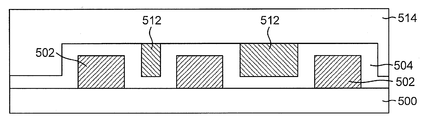
- 239000000758 substrate Substances 0.000 title claims abstract description 121
- 229910052751 metal Inorganic materials 0.000 claims abstract description 190
- 239000002184 metal Substances 0.000 claims abstract description 190
- 238000000034 method Methods 0.000 claims description 37
- 230000008569 process Effects 0.000 claims description 9
- RYGMFSIKBFXOCR-UHFFFAOYSA-N Copper Chemical compound [Cu] RYGMFSIKBFXOCR-UHFFFAOYSA-N 0.000 claims description 8
- 229910052802 copper Inorganic materials 0.000 claims description 8
- 239000010949 copper Substances 0.000 claims description 8
- 238000001771 vacuum deposition Methods 0.000 claims description 8
- 239000000463 material Substances 0.000 claims description 7
- 239000003989 dielectric material Substances 0.000 claims description 6
- 239000011368 organic material Substances 0.000 claims description 3
- 238000000206 photolithography Methods 0.000 claims description 3
- VYPSYNLAJGMNEJ-UHFFFAOYSA-N Silicium dioxide Chemical compound O=[Si]=O VYPSYNLAJGMNEJ-UHFFFAOYSA-N 0.000 claims description 2
- 238000004891 communication Methods 0.000 claims description 2
- 238000009713 electroplating Methods 0.000 claims description 2
- 229910052814 silicon oxide Inorganic materials 0.000 claims description 2
- 238000005553 drilling Methods 0.000 claims 1
- 229920002120 photoresistant polymer Polymers 0.000 description 20
- 239000004020 conductor Substances 0.000 description 8
- PXHVJJICTQNCMI-UHFFFAOYSA-N Nickel Chemical compound [Ni] PXHVJJICTQNCMI-UHFFFAOYSA-N 0.000 description 6
- 238000004519 manufacturing process Methods 0.000 description 6
- 238000005229 chemical vapour deposition Methods 0.000 description 4
- 238000000059 patterning Methods 0.000 description 4
- 239000004065 semiconductor Substances 0.000 description 4
- 238000000151 deposition Methods 0.000 description 3
- 230000008021 deposition Effects 0.000 description 3
- 230000006870 function Effects 0.000 description 3
- 229910052759 nickel Inorganic materials 0.000 description 3
- 238000012545 processing Methods 0.000 description 3
- 230000005855 radiation Effects 0.000 description 3
- 229910000679 solder Inorganic materials 0.000 description 3
- 239000004593 Epoxy Substances 0.000 description 2
- KDLHZDBZIXYQEI-UHFFFAOYSA-N Palladium Chemical compound [Pd] KDLHZDBZIXYQEI-UHFFFAOYSA-N 0.000 description 2
- 239000005380 borophosphosilicate glass Substances 0.000 description 2
- 230000008878 coupling Effects 0.000 description 2
- 238000010168 coupling process Methods 0.000 description 2
- 238000005859 coupling reaction Methods 0.000 description 2
- 238000011161 development Methods 0.000 description 2
- PCHJSUWPFVWCPO-UHFFFAOYSA-N gold Chemical compound [Au] PCHJSUWPFVWCPO-UHFFFAOYSA-N 0.000 description 2
- 229910052737 gold Inorganic materials 0.000 description 2
- 239000010931 gold Substances 0.000 description 2
- 239000005360 phosphosilicate glass Substances 0.000 description 2
- 238000005240 physical vapour deposition Methods 0.000 description 2
- 238000000623 plasma-assisted chemical vapour deposition Methods 0.000 description 2
- JBRZTFJDHDCESZ-UHFFFAOYSA-N AsGa Chemical compound [As]#[Ga] JBRZTFJDHDCESZ-UHFFFAOYSA-N 0.000 description 1
- 229910001218 Gallium arsenide Inorganic materials 0.000 description 1
- 229910000530 Gallium indium arsenide Inorganic materials 0.000 description 1
- GPXJNWSHGFTCBW-UHFFFAOYSA-N Indium phosphide Chemical compound [In]#P GPXJNWSHGFTCBW-UHFFFAOYSA-N 0.000 description 1
- XUIMIQQOPSSXEZ-UHFFFAOYSA-N Silicon Chemical compound [Si] XUIMIQQOPSSXEZ-UHFFFAOYSA-N 0.000 description 1
- ATJFFYVFTNAWJD-UHFFFAOYSA-N Tin Chemical compound [Sn] ATJFFYVFTNAWJD-UHFFFAOYSA-N 0.000 description 1
- 238000004380 ashing Methods 0.000 description 1
- 230000015572 biosynthetic process Effects 0.000 description 1
- 238000006243 chemical reaction Methods 0.000 description 1
- 238000000576 coating method Methods 0.000 description 1
- 229910017052 cobalt Inorganic materials 0.000 description 1
- 239000010941 cobalt Substances 0.000 description 1
- GUTLYIVDDKVIGB-UHFFFAOYSA-N cobalt atom Chemical compound [Co] GUTLYIVDDKVIGB-UHFFFAOYSA-N 0.000 description 1
- 230000003247 decreasing effect Effects 0.000 description 1
- 238000013461 design Methods 0.000 description 1
- 239000000945 filler Substances 0.000 description 1
- 229910052732 germanium Inorganic materials 0.000 description 1
- GNPVGFCGXDBREM-UHFFFAOYSA-N germanium atom Chemical compound [Ge] GNPVGFCGXDBREM-UHFFFAOYSA-N 0.000 description 1
- RPQDHPTXJYYUPQ-UHFFFAOYSA-N indium arsenide Chemical compound [In]#[As] RPQDHPTXJYYUPQ-UHFFFAOYSA-N 0.000 description 1
- 238000002955 isolation Methods 0.000 description 1
- 239000011133 lead Substances 0.000 description 1
- 150000002739 metals Chemical class 0.000 description 1
- 239000012811 non-conductive material Substances 0.000 description 1
- 238000004806 packaging method and process Methods 0.000 description 1
- 238000012536 packaging technology Methods 0.000 description 1
- 229910052763 palladium Inorganic materials 0.000 description 1
- 229920001690 polydopamine Polymers 0.000 description 1
- 229920000642 polymer Polymers 0.000 description 1
- 229910052710 silicon Inorganic materials 0.000 description 1
- 239000010703 silicon Substances 0.000 description 1
- HBMJWWWQQXIZIP-UHFFFAOYSA-N silicon carbide Chemical compound [Si+]#[C-] HBMJWWWQQXIZIP-UHFFFAOYSA-N 0.000 description 1
- 229910010271 silicon carbide Inorganic materials 0.000 description 1
- 229910052709 silver Inorganic materials 0.000 description 1
- 239000004332 silver Substances 0.000 description 1
- 238000005549 size reduction Methods 0.000 description 1
- 239000002904 solvent Substances 0.000 description 1
- 239000011135 tin Substances 0.000 description 1
- 238000012546 transfer Methods 0.000 description 1
Images


Classifications
-
- H—ELECTRICITY
- H01—ELECTRIC ELEMENTS
- H01L—SEMICONDUCTOR DEVICES NOT COVERED BY CLASS H10
- H01L21/00—Processes or apparatus adapted for the manufacture or treatment of semiconductor or solid state devices or of parts thereof
- H01L21/70—Manufacture or treatment of devices consisting of a plurality of solid state components formed in or on a common substrate or of parts thereof; Manufacture of integrated circuit devices or of parts thereof
- H01L21/71—Manufacture of specific parts of devices defined in group H01L21/70
- H01L21/768—Applying interconnections to be used for carrying current between separate components within a device comprising conductors and dielectrics
- H01L21/76838—Applying interconnections to be used for carrying current between separate components within a device comprising conductors and dielectrics characterised by the formation and the after-treatment of the conductors
-
- H—ELECTRICITY
- H01—ELECTRIC ELEMENTS
- H01L—SEMICONDUCTOR DEVICES NOT COVERED BY CLASS H10
- H01L21/00—Processes or apparatus adapted for the manufacture or treatment of semiconductor or solid state devices or of parts thereof
- H01L21/70—Manufacture or treatment of devices consisting of a plurality of solid state components formed in or on a common substrate or of parts thereof; Manufacture of integrated circuit devices or of parts thereof
- H01L21/71—Manufacture of specific parts of devices defined in group H01L21/70
- H01L21/768—Applying interconnections to be used for carrying current between separate components within a device comprising conductors and dielectrics
- H01L21/76801—Applying interconnections to be used for carrying current between separate components within a device comprising conductors and dielectrics characterised by the formation and the after-treatment of the dielectrics, e.g. smoothing
- H01L21/76802—Applying interconnections to be used for carrying current between separate components within a device comprising conductors and dielectrics characterised by the formation and the after-treatment of the dielectrics, e.g. smoothing by forming openings in dielectrics
-
- H—ELECTRICITY
- H01—ELECTRIC ELEMENTS
- H01L—SEMICONDUCTOR DEVICES NOT COVERED BY CLASS H10
- H01L21/00—Processes or apparatus adapted for the manufacture or treatment of semiconductor or solid state devices or of parts thereof
- H01L21/02—Manufacture or treatment of semiconductor devices or of parts thereof
- H01L21/04—Manufacture or treatment of semiconductor devices or of parts thereof the devices having potential barriers, e.g. a PN junction, depletion layer or carrier concentration layer
- H01L21/18—Manufacture or treatment of semiconductor devices or of parts thereof the devices having potential barriers, e.g. a PN junction, depletion layer or carrier concentration layer the devices having semiconductor bodies comprising elements of Group IV of the Periodic Table or AIIIBV compounds with or without impurities, e.g. doping materials
- H01L21/30—Treatment of semiconductor bodies using processes or apparatus not provided for in groups H01L21/20 - H01L21/26
- H01L21/31—Treatment of semiconductor bodies using processes or apparatus not provided for in groups H01L21/20 - H01L21/26 to form insulating layers thereon, e.g. for masking or by using photolithographic techniques; After treatment of these layers; Selection of materials for these layers
- H01L21/3205—Deposition of non-insulating-, e.g. conductive- or resistive-, layers on insulating layers; After-treatment of these layers
- H01L21/321—After treatment
- H01L21/3213—Physical or chemical etching of the layers, e.g. to produce a patterned layer from a pre-deposited extensive layer
-
- H—ELECTRICITY
- H01—ELECTRIC ELEMENTS
- H01L—SEMICONDUCTOR DEVICES NOT COVERED BY CLASS H10
- H01L21/00—Processes or apparatus adapted for the manufacture or treatment of semiconductor or solid state devices or of parts thereof
- H01L21/02—Manufacture or treatment of semiconductor devices or of parts thereof
- H01L21/04—Manufacture or treatment of semiconductor devices or of parts thereof the devices having potential barriers, e.g. a PN junction, depletion layer or carrier concentration layer
- H01L21/48—Manufacture or treatment of parts, e.g. containers, prior to assembly of the devices, using processes not provided for in a single one of the groups H01L21/18 - H01L21/326 or H10D48/04 - H10D48/07
- H01L21/4814—Conductive parts
- H01L21/4846—Leads on or in insulating or insulated substrates, e.g. metallisation
- H01L21/4857—Multilayer substrates
-
- H—ELECTRICITY
- H01—ELECTRIC ELEMENTS
- H01L—SEMICONDUCTOR DEVICES NOT COVERED BY CLASS H10
- H01L21/00—Processes or apparatus adapted for the manufacture or treatment of semiconductor or solid state devices or of parts thereof
- H01L21/70—Manufacture or treatment of devices consisting of a plurality of solid state components formed in or on a common substrate or of parts thereof; Manufacture of integrated circuit devices or of parts thereof
- H01L21/71—Manufacture of specific parts of devices defined in group H01L21/70
- H01L21/768—Applying interconnections to be used for carrying current between separate components within a device comprising conductors and dielectrics
- H01L21/76801—Applying interconnections to be used for carrying current between separate components within a device comprising conductors and dielectrics characterised by the formation and the after-treatment of the dielectrics, e.g. smoothing
- H01L21/76802—Applying interconnections to be used for carrying current between separate components within a device comprising conductors and dielectrics characterised by the formation and the after-treatment of the dielectrics, e.g. smoothing by forming openings in dielectrics
- H01L21/76816—Aspects relating to the layout of the pattern or to the size of vias or trenches
-
- H—ELECTRICITY
- H01—ELECTRIC ELEMENTS
- H01L—SEMICONDUCTOR DEVICES NOT COVERED BY CLASS H10
- H01L21/00—Processes or apparatus adapted for the manufacture or treatment of semiconductor or solid state devices or of parts thereof
- H01L21/70—Manufacture or treatment of devices consisting of a plurality of solid state components formed in or on a common substrate or of parts thereof; Manufacture of integrated circuit devices or of parts thereof
- H01L21/71—Manufacture of specific parts of devices defined in group H01L21/70
- H01L21/768—Applying interconnections to be used for carrying current between separate components within a device comprising conductors and dielectrics
- H01L21/76838—Applying interconnections to be used for carrying current between separate components within a device comprising conductors and dielectrics characterised by the formation and the after-treatment of the conductors
- H01L21/76877—Filling of holes, grooves or trenches, e.g. vias, with conductive material
- H01L21/76879—Filling of holes, grooves or trenches, e.g. vias, with conductive material by selective deposition of conductive material in the vias, e.g. selective C.V.D. on semiconductor material, plating
-
- H—ELECTRICITY
- H01—ELECTRIC ELEMENTS
- H01L—SEMICONDUCTOR DEVICES NOT COVERED BY CLASS H10
- H01L21/00—Processes or apparatus adapted for the manufacture or treatment of semiconductor or solid state devices or of parts thereof
- H01L21/70—Manufacture or treatment of devices consisting of a plurality of solid state components formed in or on a common substrate or of parts thereof; Manufacture of integrated circuit devices or of parts thereof
- H01L21/71—Manufacture of specific parts of devices defined in group H01L21/70
- H01L21/768—Applying interconnections to be used for carrying current between separate components within a device comprising conductors and dielectrics
- H01L21/76838—Applying interconnections to be used for carrying current between separate components within a device comprising conductors and dielectrics characterised by the formation and the after-treatment of the conductors
- H01L21/76885—By forming conductive members before deposition of protective insulating material, e.g. pillars, studs
-
- H—ELECTRICITY
- H01—ELECTRIC ELEMENTS
- H01L—SEMICONDUCTOR DEVICES NOT COVERED BY CLASS H10
- H01L23/00—Details of semiconductor or other solid state devices
- H01L23/48—Arrangements for conducting electric current to or from the solid state body in operation, e.g. leads, terminal arrangements ; Selection of materials therefor
- H01L23/488—Arrangements for conducting electric current to or from the solid state body in operation, e.g. leads, terminal arrangements ; Selection of materials therefor consisting of soldered or bonded constructions
- H01L23/498—Leads, i.e. metallisations or lead-frames on insulating substrates, e.g. chip carriers
- H01L23/49822—Multilayer substrates
-
- H—ELECTRICITY
- H01—ELECTRIC ELEMENTS
- H01L—SEMICONDUCTOR DEVICES NOT COVERED BY CLASS H10
- H01L23/00—Details of semiconductor or other solid state devices
- H01L23/52—Arrangements for conducting electric current within the device in operation from one component to another, i.e. interconnections, e.g. wires, lead frames
- H01L23/522—Arrangements for conducting electric current within the device in operation from one component to another, i.e. interconnections, e.g. wires, lead frames including external interconnections consisting of a multilayer structure of conductive and insulating layers inseparably formed on the semiconductor body
- H01L23/528—Layout of the interconnection structure
- H01L23/5283—Cross-sectional geometry
-
- H—ELECTRICITY
- H01—ELECTRIC ELEMENTS
- H01L—SEMICONDUCTOR DEVICES NOT COVERED BY CLASS H10
- H01L23/00—Details of semiconductor or other solid state devices
- H01L23/52—Arrangements for conducting electric current within the device in operation from one component to another, i.e. interconnections, e.g. wires, lead frames
- H01L23/522—Arrangements for conducting electric current within the device in operation from one component to another, i.e. interconnections, e.g. wires, lead frames including external interconnections consisting of a multilayer structure of conductive and insulating layers inseparably formed on the semiconductor body
- H01L23/532—Arrangements for conducting electric current within the device in operation from one component to another, i.e. interconnections, e.g. wires, lead frames including external interconnections consisting of a multilayer structure of conductive and insulating layers inseparably formed on the semiconductor body characterised by the materials
- H01L23/5329—Insulating materials
-
- H—ELECTRICITY
- H01—ELECTRIC ELEMENTS
- H01L—SEMICONDUCTOR DEVICES NOT COVERED BY CLASS H10
- H01L2224/00—Indexing scheme for arrangements for connecting or disconnecting semiconductor or solid-state bodies and methods related thereto as covered by H01L24/00
- H01L2224/01—Means for bonding being attached to, or being formed on, the surface to be connected, e.g. chip-to-package, die-attach, "first-level" interconnects; Manufacturing methods related thereto
- H01L2224/10—Bump connectors; Manufacturing methods related thereto
- H01L2224/12—Structure, shape, material or disposition of the bump connectors prior to the connecting process
- H01L2224/13—Structure, shape, material or disposition of the bump connectors prior to the connecting process of an individual bump connector
- H01L2224/13001—Core members of the bump connector
- H01L2224/13099—Material
- H01L2224/131—Material with a principal constituent of the material being a metal or a metalloid, e.g. boron [B], silicon [Si], germanium [Ge], arsenic [As], antimony [Sb], tellurium [Te] and polonium [Po], and alloys thereof
- H01L2224/13138—Material with a principal constituent of the material being a metal or a metalloid, e.g. boron [B], silicon [Si], germanium [Ge], arsenic [As], antimony [Sb], tellurium [Te] and polonium [Po], and alloys thereof the principal constituent melting at a temperature of greater than or equal to 950°C and less than 1550°C
- H01L2224/13147—Copper [Cu] as principal constituent
-
- H—ELECTRICITY
- H01—ELECTRIC ELEMENTS
- H01L—SEMICONDUCTOR DEVICES NOT COVERED BY CLASS H10
- H01L2224/00—Indexing scheme for arrangements for connecting or disconnecting semiconductor or solid-state bodies and methods related thereto as covered by H01L24/00
- H01L2224/01—Means for bonding being attached to, or being formed on, the surface to be connected, e.g. chip-to-package, die-attach, "first-level" interconnects; Manufacturing methods related thereto
- H01L2224/10—Bump connectors; Manufacturing methods related thereto
- H01L2224/15—Structure, shape, material or disposition of the bump connectors after the connecting process
- H01L2224/16—Structure, shape, material or disposition of the bump connectors after the connecting process of an individual bump connector
- H01L2224/161—Disposition
- H01L2224/16151—Disposition the bump connector connecting between a semiconductor or solid-state body and an item not being a semiconductor or solid-state body, e.g. chip-to-substrate, chip-to-passive
- H01L2224/16221—Disposition the bump connector connecting between a semiconductor or solid-state body and an item not being a semiconductor or solid-state body, e.g. chip-to-substrate, chip-to-passive the body and the item being stacked
- H01L2224/16225—Disposition the bump connector connecting between a semiconductor or solid-state body and an item not being a semiconductor or solid-state body, e.g. chip-to-substrate, chip-to-passive the body and the item being stacked the item being non-metallic, e.g. insulating substrate with or without metallisation
-
- H—ELECTRICITY
- H01—ELECTRIC ELEMENTS
- H01L—SEMICONDUCTOR DEVICES NOT COVERED BY CLASS H10
- H01L2924/00—Indexing scheme for arrangements or methods for connecting or disconnecting semiconductor or solid-state bodies as covered by H01L24/00
- H01L2924/013—Alloys
- H01L2924/014—Solder alloys
-
- H—ELECTRICITY
- H01—ELECTRIC ELEMENTS
- H01L—SEMICONDUCTOR DEVICES NOT COVERED BY CLASS H10
- H01L2924/00—Indexing scheme for arrangements or methods for connecting or disconnecting semiconductor or solid-state bodies as covered by H01L24/00
- H01L2924/10—Details of semiconductor or other solid state devices to be connected
- H01L2924/11—Device type
- H01L2924/14—Integrated circuits
-
- H—ELECTRICITY
- H01—ELECTRIC ELEMENTS
- H01L—SEMICONDUCTOR DEVICES NOT COVERED BY CLASS H10
- H01L2924/00—Indexing scheme for arrangements or methods for connecting or disconnecting semiconductor or solid-state bodies as covered by H01L24/00
- H01L2924/15—Details of package parts other than the semiconductor or other solid state devices to be connected
- H01L2924/151—Die mounting substrate
- H01L2924/153—Connection portion
- H01L2924/1531—Connection portion the connection portion being formed only on the surface of the substrate opposite to the die mounting surface
- H01L2924/15311—Connection portion the connection portion being formed only on the surface of the substrate opposite to the die mounting surface being a ball array, e.g. BGA
Landscapes
- Engineering & Computer Science (AREA)
- Physics & Mathematics (AREA)
- Microelectronics & Electronic Packaging (AREA)
- General Physics & Mathematics (AREA)
- Computer Hardware Design (AREA)
- Condensed Matter Physics & Semiconductors (AREA)
- Power Engineering (AREA)
- Manufacturing & Machinery (AREA)
- Geometry (AREA)
- Ceramic Engineering (AREA)
- Internal Circuitry In Semiconductor Integrated Circuit Devices (AREA)
- Parts Printed On Printed Circuit Boards (AREA)
- Structure Of Printed Boards (AREA)
- Manufacturing Of Printed Wiring (AREA)
Applications Claiming Priority (3)
| Application Number | Priority Date | Filing Date | Title |
|---|---|---|---|
| US14/253,798 US9269610B2 (en) | 2014-04-15 | 2014-04-15 | Pattern between pattern for low profile substrate |
| US14/253,798 | 2014-04-15 | ||
| PCT/US2015/025435 WO2015160671A1 (en) | 2014-04-15 | 2015-04-10 | Pattern between pattern for low profile substrate |
Publications (1)
| Publication Number | Publication Date |
|---|---|
| KR20160145572A true KR20160145572A (ko) | 2016-12-20 |
Family
ID=53005702
Family Applications (1)
| Application Number | Title | Priority Date | Filing Date |
|---|---|---|---|
| KR1020167028148A Withdrawn KR20160145572A (ko) | 2014-04-15 | 2015-04-10 | 낮은 프로파일 기판을 위한 패턴 사이의 패턴 |
Country Status (7)
Families Citing this family (5)
| Publication number | Priority date | Publication date | Assignee | Title |
|---|---|---|---|---|
| CN109346821A (zh) * | 2018-09-19 | 2019-02-15 | 中国科学院上海微系统与信息技术研究所 | 圆片级硅基集成小型化分形天线及其制备方法 |
| US12044965B2 (en) * | 2020-02-12 | 2024-07-23 | Hutchinson Technology Incorporated | Method for forming components without adding tabs during etching |
| US20220093505A1 (en) * | 2020-09-24 | 2022-03-24 | Intel Corporation | Via connections for staggered interconnect lines |
| US20230197602A1 (en) * | 2021-12-22 | 2023-06-22 | Intel Corporation | Staggered vertically spaced integrated circuit line metallization with differential vias & metal-selective deposition |
| US20230395506A1 (en) * | 2022-06-06 | 2023-12-07 | Intel Corporation | Self-aligned staggered integrated circuit interconnect features |
Family Cites Families (17)
| Publication number | Priority date | Publication date | Assignee | Title |
|---|---|---|---|---|
| GB2073951B (en) * | 1980-04-11 | 1984-10-03 | Hitachi Ltd | Multilayer interconnections for an integrated circuit |
| JPH0750710B2 (ja) | 1990-06-06 | 1995-05-31 | 富士ゼロックス株式会社 | 多層配線構造 |
| KR920017227A (ko) | 1991-02-05 | 1992-09-26 | 김광호 | 반도체장치의 층간콘택 구조 및 그 제조방법 |
| US6414367B1 (en) | 1999-10-28 | 2002-07-02 | National Semiconductor Corporation | Interconnect exhibiting reduced parasitic capacitance variation |
| JP2002299555A (ja) | 2001-03-30 | 2002-10-11 | Seiko Epson Corp | 集積回路およびその製造方法 |
| KR100808557B1 (ko) | 2002-05-16 | 2008-02-29 | 매그나칩 반도체 유한회사 | 엠아이엠 캐패시터 형성방법 |
| JP2005236018A (ja) * | 2004-02-19 | 2005-09-02 | Alps Electric Co Ltd | 微細配線構造および微細配線構造の製造方法 |
| JP4559757B2 (ja) | 2004-03-18 | 2010-10-13 | ルネサスエレクトロニクス株式会社 | 半導体装置およびその製造方法 |
| JP4769022B2 (ja) * | 2005-06-07 | 2011-09-07 | 京セラSlcテクノロジー株式会社 | 配線基板およびその製造方法 |
| JP2007194476A (ja) | 2006-01-20 | 2007-08-02 | Shinko Electric Ind Co Ltd | 多層配線基板の製造方法 |
| US20110215465A1 (en) * | 2010-03-03 | 2011-09-08 | Xilinx, Inc. | Multi-chip integrated circuit |
| US8377792B2 (en) * | 2010-04-07 | 2013-02-19 | National Semiconductor Corporation | Method of forming high capacitance semiconductor capacitors with a single lithography step |
| CN102986311B (zh) * | 2010-07-08 | 2016-05-04 | Lg伊诺特有限公司 | 印刷电路板及其制造方法 |
| JP2012094662A (ja) | 2010-10-26 | 2012-05-17 | Ngk Spark Plug Co Ltd | 多層配線基板の製造方法 |
| US8722505B2 (en) * | 2010-11-02 | 2014-05-13 | National Semiconductor Corporation | Semiconductor capacitor with large area plates and a small footprint that is formed with shadow masks and only two lithography steps |
| US8551856B2 (en) * | 2011-09-22 | 2013-10-08 | Northrop Grumman Systems Corporation | Embedded capacitor and method of fabricating the same |
| US9012966B2 (en) * | 2012-11-21 | 2015-04-21 | Qualcomm Incorporated | Capacitor using middle of line (MOL) conductive layers |
-
2014
- 2014-04-15 US US14/253,798 patent/US9269610B2/en active Active
-
2015
- 2015-04-10 JP JP2016562244A patent/JP2017517142A/ja active Pending
- 2015-04-10 WO PCT/US2015/025435 patent/WO2015160671A1/en active Application Filing
- 2015-04-10 BR BR112016023947A patent/BR112016023947A2/pt not_active IP Right Cessation
- 2015-04-10 CN CN201580019675.3A patent/CN106575623A/zh active Pending
- 2015-04-10 EP EP15718725.3A patent/EP3132469B1/en not_active Not-in-force
- 2015-04-10 KR KR1020167028148A patent/KR20160145572A/ko not_active Withdrawn
Also Published As
| Publication number | Publication date |
|---|---|
| US20150294933A1 (en) | 2015-10-15 |
| BR112016023947A2 (pt) | 2017-08-15 |
| WO2015160671A1 (en) | 2015-10-22 |
| JP2017517142A (ja) | 2017-06-22 |
| EP3132469A1 (en) | 2017-02-22 |
| US9269610B2 (en) | 2016-02-23 |
| CN106575623A (zh) | 2017-04-19 |
| EP3132469B1 (en) | 2019-01-09 |
| WO2015160671A9 (en) | 2016-06-09 |
Similar Documents
| Publication | Publication Date | Title |
|---|---|---|
| EP3391410B9 (en) | Semiconductor package having a variable redistribution layer thickness | |
| US10916499B2 (en) | Vias and gaps in semiconductor interconnects | |
| US9565774B2 (en) | Embedded trace substrate and method of forming the same | |
| US11694951B2 (en) | Zero-misalignment two-via structures | |
| EP3132469B1 (en) | Pattern between pattern for low profile substrate | |
| US20090321932A1 (en) | Coreless substrate package with symmetric external dielectric layers | |
| US9760002B2 (en) | Circuit board formation using organic substrates | |
| US20220302037A1 (en) | Embedded packaging structure and manufacturing method thereof | |
| US9583433B2 (en) | Integrated device package comprising conductive sheet configured as an inductor in an encapsulation layer | |
| US12176214B2 (en) | Selective metal removal for conductive interconnects in integrated circuitry | |
| CN105830213A (zh) | 包括凸块区域中的改善型通孔焊盘放置的基板 | |
| KR20150074872A (ko) | 인터포저 기판 및 그의 제조 방법 | |
| US11367682B2 (en) | Vias and gaps in semiconductor interconnects | |
| TW201307184A (zh) | 在晶圓層級封裝中用於高密度電感與重分配的薄膜結構 | |
| US8258009B2 (en) | Circuit substrate and manufacturing method thereof and package structure and manufacturing method thereof | |
| CN111128922B (zh) | 半导体装置、电路板结构及其制作方法 | |
| US20210043500A1 (en) | Multi-height interconnect trenches for resistance and capacitance optimization | |
| US20240234481A1 (en) | Semiconductor device with inductive component and method of forming | |
| US12334396B2 (en) | Unit specific variable or adaptive metal fill and system and method for the same | |
| US20230085067A1 (en) | System and method for redistribution layer (rdl) repair | |
| KR20230133169A (ko) | 유도성 컴포넌트를 가진 반도체 디바이스 및 그 형성 방법 | |
| JP4794507B2 (ja) | 半導体装置 | |
| KR20010036731A (ko) | 마이크로 수동소자의 제조 방법 |
Legal Events
| Date | Code | Title | Description |
|---|---|---|---|
| PA0105 | International application |
Patent event date: 20161010 Patent event code: PA01051R01D Comment text: International Patent Application |
|
| PG1501 | Laying open of application | ||
| PC1203 | Withdrawal of no request for examination |