EP3132469B1 - Pattern between pattern for low profile substrate - Google Patents
Pattern between pattern for low profile substrate Download PDFInfo
- Publication number
- EP3132469B1 EP3132469B1 EP15718725.3A EP15718725A EP3132469B1 EP 3132469 B1 EP3132469 B1 EP 3132469B1 EP 15718725 A EP15718725 A EP 15718725A EP 3132469 B1 EP3132469 B1 EP 3132469B1
- Authority
- EP
- European Patent Office
- Prior art keywords
- patterned metal
- metal layer
- substrate
- layer
- dielectric layer
- Prior art date
- Legal status (The legal status is an assumption and is not a legal conclusion. Google has not performed a legal analysis and makes no representation as to the accuracy of the status listed.)
- Not-in-force
Links
- 239000000758 substrate Substances 0.000 title claims description 126
- 229910052751 metal Inorganic materials 0.000 claims description 170
- 239000002184 metal Substances 0.000 claims description 170
- 238000000034 method Methods 0.000 claims description 17
- RYGMFSIKBFXOCR-UHFFFAOYSA-N Copper Chemical compound [Cu] RYGMFSIKBFXOCR-UHFFFAOYSA-N 0.000 claims description 8
- 229910052802 copper Inorganic materials 0.000 claims description 8
- 239000010949 copper Substances 0.000 claims description 8
- 230000008569 process Effects 0.000 claims description 8
- 238000001771 vacuum deposition Methods 0.000 claims description 8
- 239000000463 material Substances 0.000 claims description 7
- 239000003989 dielectric material Substances 0.000 claims description 6
- 239000011368 organic material Substances 0.000 claims description 3
- 238000000206 photolithography Methods 0.000 claims description 3
- VYPSYNLAJGMNEJ-UHFFFAOYSA-N Silicium dioxide Chemical compound O=[Si]=O VYPSYNLAJGMNEJ-UHFFFAOYSA-N 0.000 claims description 2
- 238000009713 electroplating Methods 0.000 claims description 2
- 229910052814 silicon oxide Inorganic materials 0.000 claims description 2
- 238000005553 drilling Methods 0.000 claims 1
- 229920002120 photoresistant polymer Polymers 0.000 description 20
- 239000004020 conductor Substances 0.000 description 8
- 238000004519 manufacturing process Methods 0.000 description 8
- PXHVJJICTQNCMI-UHFFFAOYSA-N Nickel Chemical compound [Ni] PXHVJJICTQNCMI-UHFFFAOYSA-N 0.000 description 6
- 238000005229 chemical vapour deposition Methods 0.000 description 4
- 239000004065 semiconductor Substances 0.000 description 4
- 238000000151 deposition Methods 0.000 description 3
- 230000008021 deposition Effects 0.000 description 3
- 229910052759 nickel Inorganic materials 0.000 description 3
- 238000000059 patterning Methods 0.000 description 3
- 238000012545 processing Methods 0.000 description 3
- 230000005855 radiation Effects 0.000 description 3
- 229910000679 solder Inorganic materials 0.000 description 3
- 239000004593 Epoxy Substances 0.000 description 2
- KDLHZDBZIXYQEI-UHFFFAOYSA-N Palladium Chemical compound [Pd] KDLHZDBZIXYQEI-UHFFFAOYSA-N 0.000 description 2
- 239000005380 borophosphosilicate glass Substances 0.000 description 2
- 230000008878 coupling Effects 0.000 description 2
- 238000010168 coupling process Methods 0.000 description 2
- 238000005859 coupling reaction Methods 0.000 description 2
- 230000003247 decreasing effect Effects 0.000 description 2
- PCHJSUWPFVWCPO-UHFFFAOYSA-N gold Chemical compound [Au] PCHJSUWPFVWCPO-UHFFFAOYSA-N 0.000 description 2
- 229910052737 gold Inorganic materials 0.000 description 2
- 239000010931 gold Substances 0.000 description 2
- 239000005360 phosphosilicate glass Substances 0.000 description 2
- 238000005240 physical vapour deposition Methods 0.000 description 2
- 238000000623 plasma-assisted chemical vapour deposition Methods 0.000 description 2
- JBRZTFJDHDCESZ-UHFFFAOYSA-N AsGa Chemical compound [As]#[Ga] JBRZTFJDHDCESZ-UHFFFAOYSA-N 0.000 description 1
- 229910000673 Indium arsenide Inorganic materials 0.000 description 1
- GPXJNWSHGFTCBW-UHFFFAOYSA-N Indium phosphide Chemical compound [In]#P GPXJNWSHGFTCBW-UHFFFAOYSA-N 0.000 description 1
- XUIMIQQOPSSXEZ-UHFFFAOYSA-N Silicon Chemical compound [Si] XUIMIQQOPSSXEZ-UHFFFAOYSA-N 0.000 description 1
- ATJFFYVFTNAWJD-UHFFFAOYSA-N Tin Chemical compound [Sn] ATJFFYVFTNAWJD-UHFFFAOYSA-N 0.000 description 1
- 238000004380 ashing Methods 0.000 description 1
- 230000015572 biosynthetic process Effects 0.000 description 1
- 238000006243 chemical reaction Methods 0.000 description 1
- 238000000576 coating method Methods 0.000 description 1
- 229910017052 cobalt Inorganic materials 0.000 description 1
- 239000010941 cobalt Substances 0.000 description 1
- GUTLYIVDDKVIGB-UHFFFAOYSA-N cobalt atom Chemical compound [Co] GUTLYIVDDKVIGB-UHFFFAOYSA-N 0.000 description 1
- 238000004891 communication Methods 0.000 description 1
- 238000013461 design Methods 0.000 description 1
- 238000011161 development Methods 0.000 description 1
- 230000008020 evaporation Effects 0.000 description 1
- 238000001704 evaporation Methods 0.000 description 1
- 230000006870 function Effects 0.000 description 1
- 229910052732 germanium Inorganic materials 0.000 description 1
- GNPVGFCGXDBREM-UHFFFAOYSA-N germanium atom Chemical compound [Ge] GNPVGFCGXDBREM-UHFFFAOYSA-N 0.000 description 1
- RPQDHPTXJYYUPQ-UHFFFAOYSA-N indium arsenide Chemical compound [In]#[As] RPQDHPTXJYYUPQ-UHFFFAOYSA-N 0.000 description 1
- 238000002955 isolation Methods 0.000 description 1
- 239000011133 lead Substances 0.000 description 1
- 150000002739 metals Chemical class 0.000 description 1
- 239000012811 non-conductive material Substances 0.000 description 1
- 238000004806 packaging method and process Methods 0.000 description 1
- 238000012536 packaging technology Methods 0.000 description 1
- 229910052763 palladium Inorganic materials 0.000 description 1
- 229920001690 polydopamine Polymers 0.000 description 1
- 229920000642 polymer Polymers 0.000 description 1
- 229910052710 silicon Inorganic materials 0.000 description 1
- 239000010703 silicon Substances 0.000 description 1
- HBMJWWWQQXIZIP-UHFFFAOYSA-N silicon carbide Chemical compound [Si+]#[C-] HBMJWWWQQXIZIP-UHFFFAOYSA-N 0.000 description 1
- 229910010271 silicon carbide Inorganic materials 0.000 description 1
- 229910052709 silver Inorganic materials 0.000 description 1
- 239000004332 silver Substances 0.000 description 1
- 238000005549 size reduction Methods 0.000 description 1
- 239000002904 solvent Substances 0.000 description 1
- 239000011135 tin Substances 0.000 description 1
- 238000012546 transfer Methods 0.000 description 1
Images


Classifications
-
- H—ELECTRICITY
- H01—ELECTRIC ELEMENTS
- H01L—SEMICONDUCTOR DEVICES NOT COVERED BY CLASS H10
- H01L21/00—Processes or apparatus adapted for the manufacture or treatment of semiconductor or solid state devices or of parts thereof
- H01L21/70—Manufacture or treatment of devices consisting of a plurality of solid state components formed in or on a common substrate or of parts thereof; Manufacture of integrated circuit devices or of parts thereof
- H01L21/71—Manufacture of specific parts of devices defined in group H01L21/70
- H01L21/768—Applying interconnections to be used for carrying current between separate components within a device comprising conductors and dielectrics
- H01L21/76801—Applying interconnections to be used for carrying current between separate components within a device comprising conductors and dielectrics characterised by the formation and the after-treatment of the dielectrics, e.g. smoothing
- H01L21/76802—Applying interconnections to be used for carrying current between separate components within a device comprising conductors and dielectrics characterised by the formation and the after-treatment of the dielectrics, e.g. smoothing by forming openings in dielectrics
-
- H—ELECTRICITY
- H01—ELECTRIC ELEMENTS
- H01L—SEMICONDUCTOR DEVICES NOT COVERED BY CLASS H10
- H01L21/00—Processes or apparatus adapted for the manufacture or treatment of semiconductor or solid state devices or of parts thereof
- H01L21/02—Manufacture or treatment of semiconductor devices or of parts thereof
- H01L21/04—Manufacture or treatment of semiconductor devices or of parts thereof the devices having potential barriers, e.g. a PN junction, depletion layer or carrier concentration layer
- H01L21/18—Manufacture or treatment of semiconductor devices or of parts thereof the devices having potential barriers, e.g. a PN junction, depletion layer or carrier concentration layer the devices having semiconductor bodies comprising elements of Group IV of the Periodic Table or AIIIBV compounds with or without impurities, e.g. doping materials
- H01L21/30—Treatment of semiconductor bodies using processes or apparatus not provided for in groups H01L21/20 - H01L21/26
- H01L21/31—Treatment of semiconductor bodies using processes or apparatus not provided for in groups H01L21/20 - H01L21/26 to form insulating layers thereon, e.g. for masking or by using photolithographic techniques; After treatment of these layers; Selection of materials for these layers
- H01L21/3205—Deposition of non-insulating-, e.g. conductive- or resistive-, layers on insulating layers; After-treatment of these layers
- H01L21/321—After treatment
- H01L21/3213—Physical or chemical etching of the layers, e.g. to produce a patterned layer from a pre-deposited extensive layer
-
- H—ELECTRICITY
- H01—ELECTRIC ELEMENTS
- H01L—SEMICONDUCTOR DEVICES NOT COVERED BY CLASS H10
- H01L21/00—Processes or apparatus adapted for the manufacture or treatment of semiconductor or solid state devices or of parts thereof
- H01L21/02—Manufacture or treatment of semiconductor devices or of parts thereof
- H01L21/04—Manufacture or treatment of semiconductor devices or of parts thereof the devices having potential barriers, e.g. a PN junction, depletion layer or carrier concentration layer
- H01L21/48—Manufacture or treatment of parts, e.g. containers, prior to assembly of the devices, using processes not provided for in a single one of the groups H01L21/18 - H01L21/326 or H10D48/04 - H10D48/07
- H01L21/4814—Conductive parts
- H01L21/4846—Leads on or in insulating or insulated substrates, e.g. metallisation
- H01L21/4857—Multilayer substrates
-
- H—ELECTRICITY
- H01—ELECTRIC ELEMENTS
- H01L—SEMICONDUCTOR DEVICES NOT COVERED BY CLASS H10
- H01L21/00—Processes or apparatus adapted for the manufacture or treatment of semiconductor or solid state devices or of parts thereof
- H01L21/70—Manufacture or treatment of devices consisting of a plurality of solid state components formed in or on a common substrate or of parts thereof; Manufacture of integrated circuit devices or of parts thereof
- H01L21/71—Manufacture of specific parts of devices defined in group H01L21/70
- H01L21/768—Applying interconnections to be used for carrying current between separate components within a device comprising conductors and dielectrics
- H01L21/76801—Applying interconnections to be used for carrying current between separate components within a device comprising conductors and dielectrics characterised by the formation and the after-treatment of the dielectrics, e.g. smoothing
- H01L21/76802—Applying interconnections to be used for carrying current between separate components within a device comprising conductors and dielectrics characterised by the formation and the after-treatment of the dielectrics, e.g. smoothing by forming openings in dielectrics
- H01L21/76816—Aspects relating to the layout of the pattern or to the size of vias or trenches
-
- H—ELECTRICITY
- H01—ELECTRIC ELEMENTS
- H01L—SEMICONDUCTOR DEVICES NOT COVERED BY CLASS H10
- H01L21/00—Processes or apparatus adapted for the manufacture or treatment of semiconductor or solid state devices or of parts thereof
- H01L21/70—Manufacture or treatment of devices consisting of a plurality of solid state components formed in or on a common substrate or of parts thereof; Manufacture of integrated circuit devices or of parts thereof
- H01L21/71—Manufacture of specific parts of devices defined in group H01L21/70
- H01L21/768—Applying interconnections to be used for carrying current between separate components within a device comprising conductors and dielectrics
- H01L21/76838—Applying interconnections to be used for carrying current between separate components within a device comprising conductors and dielectrics characterised by the formation and the after-treatment of the conductors
- H01L21/76877—Filling of holes, grooves or trenches, e.g. vias, with conductive material
- H01L21/76879—Filling of holes, grooves or trenches, e.g. vias, with conductive material by selective deposition of conductive material in the vias, e.g. selective C.V.D. on semiconductor material, plating
-
- H—ELECTRICITY
- H01—ELECTRIC ELEMENTS
- H01L—SEMICONDUCTOR DEVICES NOT COVERED BY CLASS H10
- H01L21/00—Processes or apparatus adapted for the manufacture or treatment of semiconductor or solid state devices or of parts thereof
- H01L21/70—Manufacture or treatment of devices consisting of a plurality of solid state components formed in or on a common substrate or of parts thereof; Manufacture of integrated circuit devices or of parts thereof
- H01L21/71—Manufacture of specific parts of devices defined in group H01L21/70
- H01L21/768—Applying interconnections to be used for carrying current between separate components within a device comprising conductors and dielectrics
- H01L21/76838—Applying interconnections to be used for carrying current between separate components within a device comprising conductors and dielectrics characterised by the formation and the after-treatment of the conductors
- H01L21/76885—By forming conductive members before deposition of protective insulating material, e.g. pillars, studs
-
- H—ELECTRICITY
- H01—ELECTRIC ELEMENTS
- H01L—SEMICONDUCTOR DEVICES NOT COVERED BY CLASS H10
- H01L23/00—Details of semiconductor or other solid state devices
- H01L23/48—Arrangements for conducting electric current to or from the solid state body in operation, e.g. leads, terminal arrangements ; Selection of materials therefor
- H01L23/488—Arrangements for conducting electric current to or from the solid state body in operation, e.g. leads, terminal arrangements ; Selection of materials therefor consisting of soldered or bonded constructions
- H01L23/498—Leads, i.e. metallisations or lead-frames on insulating substrates, e.g. chip carriers
- H01L23/49822—Multilayer substrates
-
- H—ELECTRICITY
- H01—ELECTRIC ELEMENTS
- H01L—SEMICONDUCTOR DEVICES NOT COVERED BY CLASS H10
- H01L23/00—Details of semiconductor or other solid state devices
- H01L23/52—Arrangements for conducting electric current within the device in operation from one component to another, i.e. interconnections, e.g. wires, lead frames
- H01L23/522—Arrangements for conducting electric current within the device in operation from one component to another, i.e. interconnections, e.g. wires, lead frames including external interconnections consisting of a multilayer structure of conductive and insulating layers inseparably formed on the semiconductor body
- H01L23/528—Layout of the interconnection structure
- H01L23/5283—Cross-sectional geometry
-
- H—ELECTRICITY
- H01—ELECTRIC ELEMENTS
- H01L—SEMICONDUCTOR DEVICES NOT COVERED BY CLASS H10
- H01L23/00—Details of semiconductor or other solid state devices
- H01L23/52—Arrangements for conducting electric current within the device in operation from one component to another, i.e. interconnections, e.g. wires, lead frames
- H01L23/522—Arrangements for conducting electric current within the device in operation from one component to another, i.e. interconnections, e.g. wires, lead frames including external interconnections consisting of a multilayer structure of conductive and insulating layers inseparably formed on the semiconductor body
- H01L23/532—Arrangements for conducting electric current within the device in operation from one component to another, i.e. interconnections, e.g. wires, lead frames including external interconnections consisting of a multilayer structure of conductive and insulating layers inseparably formed on the semiconductor body characterised by the materials
- H01L23/5329—Insulating materials
-
- H—ELECTRICITY
- H01—ELECTRIC ELEMENTS
- H01L—SEMICONDUCTOR DEVICES NOT COVERED BY CLASS H10
- H01L2224/00—Indexing scheme for arrangements for connecting or disconnecting semiconductor or solid-state bodies and methods related thereto as covered by H01L24/00
- H01L2224/01—Means for bonding being attached to, or being formed on, the surface to be connected, e.g. chip-to-package, die-attach, "first-level" interconnects; Manufacturing methods related thereto
- H01L2224/10—Bump connectors; Manufacturing methods related thereto
- H01L2224/12—Structure, shape, material or disposition of the bump connectors prior to the connecting process
- H01L2224/13—Structure, shape, material or disposition of the bump connectors prior to the connecting process of an individual bump connector
- H01L2224/13001—Core members of the bump connector
- H01L2224/13099—Material
- H01L2224/131—Material with a principal constituent of the material being a metal or a metalloid, e.g. boron [B], silicon [Si], germanium [Ge], arsenic [As], antimony [Sb], tellurium [Te] and polonium [Po], and alloys thereof
- H01L2224/13138—Material with a principal constituent of the material being a metal or a metalloid, e.g. boron [B], silicon [Si], germanium [Ge], arsenic [As], antimony [Sb], tellurium [Te] and polonium [Po], and alloys thereof the principal constituent melting at a temperature of greater than or equal to 950°C and less than 1550°C
- H01L2224/13147—Copper [Cu] as principal constituent
-
- H—ELECTRICITY
- H01—ELECTRIC ELEMENTS
- H01L—SEMICONDUCTOR DEVICES NOT COVERED BY CLASS H10
- H01L2224/00—Indexing scheme for arrangements for connecting or disconnecting semiconductor or solid-state bodies and methods related thereto as covered by H01L24/00
- H01L2224/01—Means for bonding being attached to, or being formed on, the surface to be connected, e.g. chip-to-package, die-attach, "first-level" interconnects; Manufacturing methods related thereto
- H01L2224/10—Bump connectors; Manufacturing methods related thereto
- H01L2224/15—Structure, shape, material or disposition of the bump connectors after the connecting process
- H01L2224/16—Structure, shape, material or disposition of the bump connectors after the connecting process of an individual bump connector
- H01L2224/161—Disposition
- H01L2224/16151—Disposition the bump connector connecting between a semiconductor or solid-state body and an item not being a semiconductor or solid-state body, e.g. chip-to-substrate, chip-to-passive
- H01L2224/16221—Disposition the bump connector connecting between a semiconductor or solid-state body and an item not being a semiconductor or solid-state body, e.g. chip-to-substrate, chip-to-passive the body and the item being stacked
- H01L2224/16225—Disposition the bump connector connecting between a semiconductor or solid-state body and an item not being a semiconductor or solid-state body, e.g. chip-to-substrate, chip-to-passive the body and the item being stacked the item being non-metallic, e.g. insulating substrate with or without metallisation
-
- H—ELECTRICITY
- H01—ELECTRIC ELEMENTS
- H01L—SEMICONDUCTOR DEVICES NOT COVERED BY CLASS H10
- H01L2924/00—Indexing scheme for arrangements or methods for connecting or disconnecting semiconductor or solid-state bodies as covered by H01L24/00
- H01L2924/013—Alloys
- H01L2924/014—Solder alloys
-
- H—ELECTRICITY
- H01—ELECTRIC ELEMENTS
- H01L—SEMICONDUCTOR DEVICES NOT COVERED BY CLASS H10
- H01L2924/00—Indexing scheme for arrangements or methods for connecting or disconnecting semiconductor or solid-state bodies as covered by H01L24/00
- H01L2924/10—Details of semiconductor or other solid state devices to be connected
- H01L2924/11—Device type
- H01L2924/14—Integrated circuits
-
- H—ELECTRICITY
- H01—ELECTRIC ELEMENTS
- H01L—SEMICONDUCTOR DEVICES NOT COVERED BY CLASS H10
- H01L2924/00—Indexing scheme for arrangements or methods for connecting or disconnecting semiconductor or solid-state bodies as covered by H01L24/00
- H01L2924/15—Details of package parts other than the semiconductor or other solid state devices to be connected
- H01L2924/151—Die mounting substrate
- H01L2924/153—Connection portion
- H01L2924/1531—Connection portion the connection portion being formed only on the surface of the substrate opposite to the die mounting surface
- H01L2924/15311—Connection portion the connection portion being formed only on the surface of the substrate opposite to the die mounting surface being a ball array, e.g. BGA
Definitions
- This application relates to substrates in integrated circuit devices, and more particularly, to substrates that include a metal pattern in between a metal pattern to provide a low profile substrate.
- Photolithography produces a three-dimensional pattern on a surface of a substrate using a light-sensitive photoresist material and controlled exposure to light.
- the resist is applied on the substrate surface as a polymer solution.
- the resist is then baked, which drives out the solvent.
- the resist is exposed to controlled light.
- the light passes through a mask that defines the desired pattern.
- the pattern is transferred to the resist, and the resist is used to transfer the pattern to the underlying substrate. In this way, layers can be built one on top of another to form the desired IC device.
- Patterned conductive material on one level is typically electrically insulated from patterned conductive material on another level by a layer of dielectric material.
- Figure 1 illustrates an IC substrate 100 having a first patterned metal layer 104 and a second patterned metal layer 108 according to the prior art.
- the first patterned metal layer 104 is formed on a substrate 102.
- a dielectric layer 106 is formed over the first patterned metal layer 104 and separates the second patterned metal layer 108 from the first patterned metal layer 104.
- the second patterned metal layer 108 is formed on the dielectric material 106.
- the space 110 between the two patterned metal layers is occupied only by dielectric material 106, taking up space and adding unwanted thickness to the IC substrate 100.
- Figures 2A-2J illustrate a method that is typically used to form patterned metal layers on a substrate.
- a substrate 200 with a first metal layer 202 formed on the substrate 200 is provided.
- a photoresist layer 204 is formed on top of the first metal layer 202, and in Figure 2C , the photoresist layer 204 is patterned to include various openings that expose portions of the first metal layer 202 to subsequent etch.
- the first metal layer 202 is patterned using the photoresist layer 204.
- the photoresist layer 204 is removed, leaving the first patterned metal layer 202.
- a dielectric layer 206 is formed over the first patterned metal layer 202.
- a photoresist layer 208 is formed on top of the dielectric layer 206.
- the photoresist layer 208 is patterned and etched to expose portions of the dielectric layer 206.
- a second metal 210 is deposited on the exposed portions of the dielectric layer 206, and in Figure 2I , the photoresist layer 208 is removed, leaving the second patterned metal layer 210 and the first patterned metal layer 202, with the dielectric layer 206 separating the two metal layers.
- US 6414367 discloses an arrangement including a first patterned layer provided on a substrate.
- a dielectric layer is formed on the first patterned layer, the top surface of the dielectric layer being parallel to the top surface of the substrate.
- a second patterned layer is formed on the dielectric layer and extends between portions of the first patterned layer, being separated from the first patterned layer by the thickness of the dielectric layer.
- a non-conductive layer is provided over the top surface of the dielectic layer.
- an IC substrate that includes a second patterned metal layer formed in between a first patterned metal layer.
- portions of the second patterned metal layer are located in the middle of portions of the first patterned metal layer.
- a dielectric layer separates the first patterned metal layer from the second patterned metal layer.
- a non-conductive layer is formed on the dielectric layer and the second patterned metal layer.
- the metal layers comprise copper.
- the IC substrate comprises a package substrate such as an organic substrate.
- the IC substrate may comprise a semiconductor substrate (a die).
- the IC substrate of the present disclosure not only has a reduced height, but also has improved routing density, greater mechanical stability, and improved electrical performance.
- the dielectric layer is thinner than in traditional implementations and allows the second patterned metal layer to be closer to the first patterned metal layer.
- the dielectric layer is uniform in thickness. In an exemplary embodiment, the dielectric layer is about 10 ⁇ m thick.
- the dielectric layer conforms to the shape of the first patterned metal layer. Vacuum coating may be used to form the dielectric layer.
- an IC substrate that includes a second patterned metal layer formed in between a first patterned metal layer.
- a dielectric layer separates the first patterned metal layer from the second patterned metal layer.
- the dielectric layer is a means for separating and electrically isolating the first patterned metal layer from the second patterned metal layer.
- a non-conductive layer is formed on the dielectric layer and the second patterned metal layer.
- the IC substrate comprises a package substrate such as an organic substrate.
- the IC substrate may comprise a die substrate.
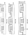
- Figure 3A shows an example IC substrate 300 comprising a substrate 302, a first patterned metal layer 304, a dielectric layer 306, a second patterned metal layer 308, and a non-conductive layer 310.
- the metal layers 304, 308 may comprise copper, nickel, or other suitable metals for conducting such as silver or gold.
- the dielectric layer 306 covers and conforms to the shape of the first patterned metal layer 306.
- the dielectric layer 306 typically includes an oxide (e.g., silicon oxide), or any other suitable material such as phosphosilicate glass (PSG) or borophosphosilicate glass (BPSG).
- the second patterned metal layer 308 is formed on the dielectric layer 306, extends past the first patterned metal layer 304, and is substantially parallel to the first patterned metal layer 304.
- the second patterned metal layer 308 is formed in between the first patterned metal layer 304,
- the non-conductive layer 310 is formed on the second patterned metal layer 308 and the dielectric layer 306.
- the non-conductive layer 310 comprises a dielectric material, a prepreg material (e.g., epoxy), an organic material, or a combination thereof.
- the substrate 302 may include a package substrate or a die substrate.
- the substrate 302 may comprise a wide variety of forms such as an organic substrate or a semiconductor substrate.
- the substrate 302 includes conductive layers (e.g., first and second patterned metal layers 304, 308) to carry power, ground, and signals through the substrate 302.
- the conductive layers are formed from copper, although other conductive materials such as tin, lead, nickel, gold, palladium, or other materials may be used.
- Non-conductive material in the substrate 302 may be formed from organic materials, such as epoxy material.
- the substrate 302 may include suitable semiconductor materials such as silicon, germanium, silicon carbide, gallium arsenic, indium arsenide, and indium phosphide.
- the substrate 302 may include a variety of other features such as p-type doped regions and/or n-type doped regions, isolation features, gate stacks, inter-level dielectric (ILD) layers, and conductive features (e.g., first and second patterned metal layers 304, 308).
- suitable semiconductor materials such as silicon, germanium, silicon carbide, gallium arsenic, indium arsenide, and indium phosphide.
- the substrate 302 may include a variety of other features such as p-type doped regions and/or n-type doped regions, isolation features, gate stacks, inter-level dielectric (ILD) layers, and conductive features (e.g., first and second patterned metal layers 304, 308).
- ILD inter-level dielectric
- the space typically occupied by only dielectric material is now used and includes a second patterned metal layer 308.
- This space can be used because the dielectric layer 306 is coated onto the first patterned metal layer 304 to conform to the shape of the first patterned metal layer 304.
- the dielectric layer was blanket deposited to cover the first patterned metal layer to form a thick dielectric block, regardless of the shape of the first patterned metal layer.
- the dielectric layer 306 formed over the first patterned metal layer 304 is thinner than in traditional implementations and allows the second patterned metal layer 308 to be closer to the first patterned metal layer 304. Hence, the second patterned metal layer 308 can be formed in between the first patterned metal layer 304.
- the dielectric layer 306 is about 10 ⁇ m thick.
- the thinner dielectric layer 306 and metal layers 304, 308 that are spaced closer together provide an IC substrate with a reduced thickness/height.
- the dielectric layer 306 can still serve as a guard rail that reduces coupling and interference for high speed/critical signal routing without an increase in the substrate area.
- the IC substrate 300 has improved routing density (e.g., more features are provided in an area). This increased density provides greater mechanical stability to the IC substrate 300.
- the IC substrate 300 has improved electrical performance. For example, there is decreased loop inductance of conductive lines (e.g., metal layers 304, 308) in the substrate 300 because the conductive lines are closer together. When the conductive lines are closer together, the loop through which current travels is made smaller. A larger loop creates a stronger magnetic field, and results in a greater inductance than a smaller loop. In package substrate embodiments, there is reduced package inductance because of thinner package thickness. Moreover, better tolerance/control and reduced coupling distance can be used in designing directional couplers, filter, and inductors without an increase in substrate area.
- the dielectric layer 306 is coated onto the first patterned metal layer 304 in a uniform thickness.
- the thickness T1 is substantially the same as the thickness T2.
- very controlled dielectric processing such as vacuum coating
- the thickness of dielectric layer 306 can be made very uniform.
- This controlled dielectric processing allows the formation of both thick and fine line metal patterns.
- the second patterned metal layer 308 includes a portion having a larger width W1 and a thinner width W2.
- the second patterned metal layer 308 includes portions having substantially the same width.
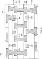
- Figure 3B illustrates an IC substrate 300 having a substrate 302 built up with second patterned metal layers 308 formed in between first patterned metal layers 304 to provide a low profile substrate having a reduced thickness or height.
- the first patterned metal layers 304 are separated from the second patterned metal layers 308 by dielectric layers 306.
- Non-conductive layers 310 are formed over the second patterned metal layers 308.
- the first patterned metal layers 304 are coupled to the second patterned metal layers 308 through vias 312.
- the thickness of an IC substrate prepared according to traditional implementations is about 656 microns.
- the thickness of the substrate is reduced to about 586 microns. This is a difference in thickness of about 70 microns or about 10.7%.
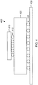
- Figure 4 illustrates a flip-chip package 400 that includes a substrate in accordance with one or more embodiments of the present disclosure.
- Package 400 includes a die substrate 410 (e.g., an integrated circuit die) and a package substrate 420 such as an organic package substrate.
- Die 410 electrically (and mechanically) interconnects with package substrate 420 by means of solder bumps 412 as known in the flip-chip packaging arts.
- bumps 412 may be replaced by copper pillars or other suitable interconnects.
- package 400 includes a means for conductively interconnecting die 410 to package substrate 420 such as through the use of bumps 412 (e.g., solder bumps, or copper pillars).
- Package substrate 420 couples to a printed circuit board 330 via solder balls 422.
- the die substrate 410 includes a substrate with patterned metal layers formed in between other patterned metal layers according to the present disclosure.
- the package substrate 420 includes a substrate with patterned metal layers formed in between other patterned metal layers according to the present disclosure.
- both the die substrate 410 and the package substrate 420 include a substrate with patterned metal layers formed in between other patterned metal layers according to the present disclosure.
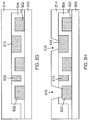
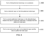
- a manufacturing process generic to the various embodiments discussed herein may be summarized as shown in a flowchart of Figure 6 .
- a first step 600 comprises forming a first patterned metal layer on a substrate. This step is illustrated, for example, in Figure 5A .
- a second step 605 comprises forming a dielectric layer on the first patterned metal layer. An example of this step is shown in Figure 5A .
- the dielectric layer is formed onto the first patterned metal layer using vacuum coating.
- the dielectric layers formed using vacuum coating may have a uniform thickness.
- the process includes a step 610 of forming a second patterned metal layer on the dielectric layer.
- the second patterned metal layer is formed between the first patterned metal layer. This step is illustrated, for example, in Figures 5C-5F .
- the process includes a step 615 of forming a non-conductive layer on the dielectric layer and the second patterned metal layer. This step is illustrated, for example, in Figure 5G .
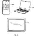
- Integrated circuit packages including an IC substrate as disclosed herein may be incorporated into a wide variety of electronic systems.
- a cell phone 700, a laptop 705, and a tablet PC 710 may all include an integrated circuit package incorporating a substrate constructed in accordance with the disclosure.
- Other exemplary electronic systems such as a music player, a video player, a communication device, and a personal computer may also be configured with integrated circuit packages constructed in accordance with the disclosure.
Landscapes
- Engineering & Computer Science (AREA)
- Physics & Mathematics (AREA)
- Microelectronics & Electronic Packaging (AREA)
- General Physics & Mathematics (AREA)
- Condensed Matter Physics & Semiconductors (AREA)
- Computer Hardware Design (AREA)
- Power Engineering (AREA)
- Manufacturing & Machinery (AREA)
- Geometry (AREA)
- Ceramic Engineering (AREA)
- Internal Circuitry In Semiconductor Integrated Circuit Devices (AREA)
- Parts Printed On Printed Circuit Boards (AREA)
- Structure Of Printed Boards (AREA)
- Manufacturing Of Printed Wiring (AREA)
Applications Claiming Priority (2)
| Application Number | Priority Date | Filing Date | Title |
|---|---|---|---|
| US14/253,798 US9269610B2 (en) | 2014-04-15 | 2014-04-15 | Pattern between pattern for low profile substrate |
| PCT/US2015/025435 WO2015160671A1 (en) | 2014-04-15 | 2015-04-10 | Pattern between pattern for low profile substrate |
Publications (2)
| Publication Number | Publication Date |
|---|---|
| EP3132469A1 EP3132469A1 (en) | 2017-02-22 |
| EP3132469B1 true EP3132469B1 (en) | 2019-01-09 |
Family
ID=53005702
Family Applications (1)
| Application Number | Title | Priority Date | Filing Date |
|---|---|---|---|
| EP15718725.3A Not-in-force EP3132469B1 (en) | 2014-04-15 | 2015-04-10 | Pattern between pattern for low profile substrate |
Country Status (7)
Families Citing this family (5)
| Publication number | Priority date | Publication date | Assignee | Title |
|---|---|---|---|---|
| CN109346821A (zh) * | 2018-09-19 | 2019-02-15 | 中国科学院上海微系统与信息技术研究所 | 圆片级硅基集成小型化分形天线及其制备方法 |
| US12044965B2 (en) * | 2020-02-12 | 2024-07-23 | Hutchinson Technology Incorporated | Method for forming components without adding tabs during etching |
| US20220093505A1 (en) * | 2020-09-24 | 2022-03-24 | Intel Corporation | Via connections for staggered interconnect lines |
| US20230197602A1 (en) * | 2021-12-22 | 2023-06-22 | Intel Corporation | Staggered vertically spaced integrated circuit line metallization with differential vias & metal-selective deposition |
| US20230395506A1 (en) * | 2022-06-06 | 2023-12-07 | Intel Corporation | Self-aligned staggered integrated circuit interconnect features |
Family Cites Families (17)
| Publication number | Priority date | Publication date | Assignee | Title |
|---|---|---|---|---|
| GB2073951B (en) * | 1980-04-11 | 1984-10-03 | Hitachi Ltd | Multilayer interconnections for an integrated circuit |
| JPH0750710B2 (ja) | 1990-06-06 | 1995-05-31 | 富士ゼロックス株式会社 | 多層配線構造 |
| KR920017227A (ko) | 1991-02-05 | 1992-09-26 | 김광호 | 반도체장치의 층간콘택 구조 및 그 제조방법 |
| US6414367B1 (en) | 1999-10-28 | 2002-07-02 | National Semiconductor Corporation | Interconnect exhibiting reduced parasitic capacitance variation |
| JP2002299555A (ja) | 2001-03-30 | 2002-10-11 | Seiko Epson Corp | 集積回路およびその製造方法 |
| KR100808557B1 (ko) | 2002-05-16 | 2008-02-29 | 매그나칩 반도체 유한회사 | 엠아이엠 캐패시터 형성방법 |
| JP2005236018A (ja) * | 2004-02-19 | 2005-09-02 | Alps Electric Co Ltd | 微細配線構造および微細配線構造の製造方法 |
| JP4559757B2 (ja) | 2004-03-18 | 2010-10-13 | ルネサスエレクトロニクス株式会社 | 半導体装置およびその製造方法 |
| JP4769022B2 (ja) * | 2005-06-07 | 2011-09-07 | 京セラSlcテクノロジー株式会社 | 配線基板およびその製造方法 |
| JP2007194476A (ja) | 2006-01-20 | 2007-08-02 | Shinko Electric Ind Co Ltd | 多層配線基板の製造方法 |
| US20110215465A1 (en) * | 2010-03-03 | 2011-09-08 | Xilinx, Inc. | Multi-chip integrated circuit |
| US8377792B2 (en) * | 2010-04-07 | 2013-02-19 | National Semiconductor Corporation | Method of forming high capacitance semiconductor capacitors with a single lithography step |
| CN102986311B (zh) * | 2010-07-08 | 2016-05-04 | Lg伊诺特有限公司 | 印刷电路板及其制造方法 |
| JP2012094662A (ja) | 2010-10-26 | 2012-05-17 | Ngk Spark Plug Co Ltd | 多層配線基板の製造方法 |
| US8722505B2 (en) * | 2010-11-02 | 2014-05-13 | National Semiconductor Corporation | Semiconductor capacitor with large area plates and a small footprint that is formed with shadow masks and only two lithography steps |
| US8551856B2 (en) * | 2011-09-22 | 2013-10-08 | Northrop Grumman Systems Corporation | Embedded capacitor and method of fabricating the same |
| US9012966B2 (en) * | 2012-11-21 | 2015-04-21 | Qualcomm Incorporated | Capacitor using middle of line (MOL) conductive layers |
-
2014
- 2014-04-15 US US14/253,798 patent/US9269610B2/en active Active
-
2015
- 2015-04-10 JP JP2016562244A patent/JP2017517142A/ja active Pending
- 2015-04-10 WO PCT/US2015/025435 patent/WO2015160671A1/en active Application Filing
- 2015-04-10 BR BR112016023947A patent/BR112016023947A2/pt not_active IP Right Cessation
- 2015-04-10 CN CN201580019675.3A patent/CN106575623A/zh active Pending
- 2015-04-10 EP EP15718725.3A patent/EP3132469B1/en not_active Not-in-force
- 2015-04-10 KR KR1020167028148A patent/KR20160145572A/ko not_active Withdrawn
Non-Patent Citations (1)
| Title |
|---|
| None * |
Also Published As
| Publication number | Publication date |
|---|---|
| US20150294933A1 (en) | 2015-10-15 |
| BR112016023947A2 (pt) | 2017-08-15 |
| WO2015160671A1 (en) | 2015-10-22 |
| JP2017517142A (ja) | 2017-06-22 |
| EP3132469A1 (en) | 2017-02-22 |
| US9269610B2 (en) | 2016-02-23 |
| CN106575623A (zh) | 2017-04-19 |
| KR20160145572A (ko) | 2016-12-20 |
| WO2015160671A9 (en) | 2016-06-09 |
Similar Documents
| Publication | Publication Date | Title |
|---|---|---|
| US11270953B2 (en) | Structure and formation method of chip package with shielding structure | |
| US10916499B2 (en) | Vias and gaps in semiconductor interconnects | |
| US10553538B2 (en) | Semiconductor package having a variable redistribution layer thickness | |
| EP3132469B1 (en) | Pattern between pattern for low profile substrate | |
| US12176214B2 (en) | Selective metal removal for conductive interconnects in integrated circuitry | |
| US8129835B2 (en) | Package substrate having semiconductor component embedded therein and fabrication method thereof | |
| EP4064342A1 (en) | Integrated circuit package redistribution layers with metal-insulator-metal (mim) capacitors | |
| CN105830213A (zh) | 包括凸块区域中的改善型通孔焊盘放置的基板 | |
| US20200411317A1 (en) | Integrated circuit package assemblies with high-aspect ratio metallization features | |
| KR20150074872A (ko) | 인터포저 기판 및 그의 제조 방법 | |
| US10667406B2 (en) | Circuit board and method for manufacturing the same | |
| US11367682B2 (en) | Vias and gaps in semiconductor interconnects | |
| CN111128922B (zh) | 半导体装置、电路板结构及其制作方法 | |
| US20210043500A1 (en) | Multi-height interconnect trenches for resistance and capacitance optimization | |
| US20200091062A1 (en) | Integrated circuit cavity formation with multiple interconnection pads | |
| US20240234481A1 (en) | Semiconductor device with inductive component and method of forming | |
| CN117133524A (zh) | 片上电感器结构及其制作方法 | |
| KR20010036731A (ko) | 마이크로 수동소자의 제조 방법 |
Legal Events
| Date | Code | Title | Description |
|---|---|---|---|
| STAA | Information on the status of an ep patent application or granted ep patent |
Free format text: STATUS: THE INTERNATIONAL PUBLICATION HAS BEEN MADE |
|
| PUAI | Public reference made under article 153(3) epc to a published international application that has entered the european phase |
Free format text: ORIGINAL CODE: 0009012 |
|
| STAA | Information on the status of an ep patent application or granted ep patent |
Free format text: STATUS: REQUEST FOR EXAMINATION WAS MADE |
|
| 17P | Request for examination filed |
Effective date: 20160926 |
|
| AK | Designated contracting states |
Kind code of ref document: A1 Designated state(s): AL AT BE BG CH CY CZ DE DK EE ES FI FR GB GR HR HU IE IS IT LI LT LU LV MC MK MT NL NO PL PT RO RS SE SI SK SM TR |
|
| AX | Request for extension of the european patent |
Extension state: BA ME |
|
| DAV | Request for validation of the european patent (deleted) | ||
| DAX | Request for extension of the european patent (deleted) | ||
| STAA | Information on the status of an ep patent application or granted ep patent |
Free format text: STATUS: EXAMINATION IS IN PROGRESS |
|
| 17Q | First examination report despatched |
Effective date: 20170807 |
|
| GRAP | Despatch of communication of intention to grant a patent |
Free format text: ORIGINAL CODE: EPIDOSNIGR1 |
|
| STAA | Information on the status of an ep patent application or granted ep patent |
Free format text: STATUS: GRANT OF PATENT IS INTENDED |
|
| INTG | Intention to grant announced |
Effective date: 20180801 |
|
| GRAS | Grant fee paid |
Free format text: ORIGINAL CODE: EPIDOSNIGR3 |
|
| GRAA | (expected) grant |
Free format text: ORIGINAL CODE: 0009210 |
|
| STAA | Information on the status of an ep patent application or granted ep patent |
Free format text: STATUS: THE PATENT HAS BEEN GRANTED |
|
| AK | Designated contracting states |
Kind code of ref document: B1 Designated state(s): AL AT BE BG CH CY CZ DE DK EE ES FI FR GB GR HR HU IE IS IT LI LT LU LV MC MK MT NL NO PL PT RO RS SE SI SK SM TR |
|
| REG | Reference to a national code |
Ref country code: GB Ref legal event code: FG4D |
|
| REG | Reference to a national code |
Ref country code: CH Ref legal event code: EP Ref country code: AT Ref legal event code: REF Ref document number: 1088385 Country of ref document: AT Kind code of ref document: T Effective date: 20190115 |
|
| REG | Reference to a national code |
Ref country code: IE Ref legal event code: FG4D |
|
| REG | Reference to a national code |
Ref country code: DE Ref legal event code: R096 Ref document number: 602015023174 Country of ref document: DE |
|
| PGFP | Annual fee paid to national office [announced via postgrant information from national office to epo] |
Ref country code: GB Payment date: 20190211 Year of fee payment: 5 |
|
| REG | Reference to a national code |
Ref country code: NL Ref legal event code: MP Effective date: 20190109 |
|
| REG | Reference to a national code |
Ref country code: LT Ref legal event code: MG4D |
|
| PG25 | Lapsed in a contracting state [announced via postgrant information from national office to epo] |
Ref country code: NL Free format text: LAPSE BECAUSE OF FAILURE TO SUBMIT A TRANSLATION OF THE DESCRIPTION OR TO PAY THE FEE WITHIN THE PRESCRIBED TIME-LIMIT Effective date: 20190109 |
|
| REG | Reference to a national code |
Ref country code: AT Ref legal event code: MK05 Ref document number: 1088385 Country of ref document: AT Kind code of ref document: T Effective date: 20190109 |
|
| PG25 | Lapsed in a contracting state [announced via postgrant information from national office to epo] |
Ref country code: PL Free format text: LAPSE BECAUSE OF FAILURE TO SUBMIT A TRANSLATION OF THE DESCRIPTION OR TO PAY THE FEE WITHIN THE PRESCRIBED TIME-LIMIT Effective date: 20190109 Ref country code: LT Free format text: LAPSE BECAUSE OF FAILURE TO SUBMIT A TRANSLATION OF THE DESCRIPTION OR TO PAY THE FEE WITHIN THE PRESCRIBED TIME-LIMIT Effective date: 20190109 Ref country code: SE Free format text: LAPSE BECAUSE OF FAILURE TO SUBMIT A TRANSLATION OF THE DESCRIPTION OR TO PAY THE FEE WITHIN THE PRESCRIBED TIME-LIMIT Effective date: 20190109 Ref country code: FI Free format text: LAPSE BECAUSE OF FAILURE TO SUBMIT A TRANSLATION OF THE DESCRIPTION OR TO PAY THE FEE WITHIN THE PRESCRIBED TIME-LIMIT Effective date: 20190109 Ref country code: ES Free format text: LAPSE BECAUSE OF FAILURE TO SUBMIT A TRANSLATION OF THE DESCRIPTION OR TO PAY THE FEE WITHIN THE PRESCRIBED TIME-LIMIT Effective date: 20190109 Ref country code: PT Free format text: LAPSE BECAUSE OF FAILURE TO SUBMIT A TRANSLATION OF THE DESCRIPTION OR TO PAY THE FEE WITHIN THE PRESCRIBED TIME-LIMIT Effective date: 20190509 Ref country code: NO Free format text: LAPSE BECAUSE OF FAILURE TO SUBMIT A TRANSLATION OF THE DESCRIPTION OR TO PAY THE FEE WITHIN THE PRESCRIBED TIME-LIMIT Effective date: 20190409 |
|
| PG25 | Lapsed in a contracting state [announced via postgrant information from national office to epo] |
Ref country code: GR Free format text: LAPSE BECAUSE OF FAILURE TO SUBMIT A TRANSLATION OF THE DESCRIPTION OR TO PAY THE FEE WITHIN THE PRESCRIBED TIME-LIMIT Effective date: 20190410 Ref country code: LV Free format text: LAPSE BECAUSE OF FAILURE TO SUBMIT A TRANSLATION OF THE DESCRIPTION OR TO PAY THE FEE WITHIN THE PRESCRIBED TIME-LIMIT Effective date: 20190109 Ref country code: IS Free format text: LAPSE BECAUSE OF FAILURE TO SUBMIT A TRANSLATION OF THE DESCRIPTION OR TO PAY THE FEE WITHIN THE PRESCRIBED TIME-LIMIT Effective date: 20190509 Ref country code: HR Free format text: LAPSE BECAUSE OF FAILURE TO SUBMIT A TRANSLATION OF THE DESCRIPTION OR TO PAY THE FEE WITHIN THE PRESCRIBED TIME-LIMIT Effective date: 20190109 Ref country code: RS Free format text: LAPSE BECAUSE OF FAILURE TO SUBMIT A TRANSLATION OF THE DESCRIPTION OR TO PAY THE FEE WITHIN THE PRESCRIBED TIME-LIMIT Effective date: 20190109 Ref country code: BG Free format text: LAPSE BECAUSE OF FAILURE TO SUBMIT A TRANSLATION OF THE DESCRIPTION OR TO PAY THE FEE WITHIN THE PRESCRIBED TIME-LIMIT Effective date: 20190409 |
|
| REG | Reference to a national code |
Ref country code: DE Ref legal event code: R097 Ref document number: 602015023174 Country of ref document: DE |
|
| PG25 | Lapsed in a contracting state [announced via postgrant information from national office to epo] |
Ref country code: AL Free format text: LAPSE BECAUSE OF FAILURE TO SUBMIT A TRANSLATION OF THE DESCRIPTION OR TO PAY THE FEE WITHIN THE PRESCRIBED TIME-LIMIT Effective date: 20190109 Ref country code: AT Free format text: LAPSE BECAUSE OF FAILURE TO SUBMIT A TRANSLATION OF THE DESCRIPTION OR TO PAY THE FEE WITHIN THE PRESCRIBED TIME-LIMIT Effective date: 20190109 Ref country code: CZ Free format text: LAPSE BECAUSE OF FAILURE TO SUBMIT A TRANSLATION OF THE DESCRIPTION OR TO PAY THE FEE WITHIN THE PRESCRIBED TIME-LIMIT Effective date: 20190109 Ref country code: RO Free format text: LAPSE BECAUSE OF FAILURE TO SUBMIT A TRANSLATION OF THE DESCRIPTION OR TO PAY THE FEE WITHIN THE PRESCRIBED TIME-LIMIT Effective date: 20190109 Ref country code: SK Free format text: LAPSE BECAUSE OF FAILURE TO SUBMIT A TRANSLATION OF THE DESCRIPTION OR TO PAY THE FEE WITHIN THE PRESCRIBED TIME-LIMIT Effective date: 20190109 Ref country code: EE Free format text: LAPSE BECAUSE OF FAILURE TO SUBMIT A TRANSLATION OF THE DESCRIPTION OR TO PAY THE FEE WITHIN THE PRESCRIBED TIME-LIMIT Effective date: 20190109 Ref country code: IT Free format text: LAPSE BECAUSE OF FAILURE TO SUBMIT A TRANSLATION OF THE DESCRIPTION OR TO PAY THE FEE WITHIN THE PRESCRIBED TIME-LIMIT Effective date: 20190109 Ref country code: DK Free format text: LAPSE BECAUSE OF FAILURE TO SUBMIT A TRANSLATION OF THE DESCRIPTION OR TO PAY THE FEE WITHIN THE PRESCRIBED TIME-LIMIT Effective date: 20190109 |
|
| REG | Reference to a national code |
Ref country code: DE Ref legal event code: R119 Ref document number: 602015023174 Country of ref document: DE |
|
| PLBE | No opposition filed within time limit |
Free format text: ORIGINAL CODE: 0009261 |
|
| STAA | Information on the status of an ep patent application or granted ep patent |
Free format text: STATUS: NO OPPOSITION FILED WITHIN TIME LIMIT |
|
| PG25 | Lapsed in a contracting state [announced via postgrant information from national office to epo] |
Ref country code: SM Free format text: LAPSE BECAUSE OF FAILURE TO SUBMIT A TRANSLATION OF THE DESCRIPTION OR TO PAY THE FEE WITHIN THE PRESCRIBED TIME-LIMIT Effective date: 20190109 |
|
| REG | Reference to a national code |
Ref country code: CH Ref legal event code: PL |
|
| 26N | No opposition filed |
Effective date: 20191010 |
|
| REG | Reference to a national code |
Ref country code: BE Ref legal event code: MM Effective date: 20190430 |
|
| PG25 | Lapsed in a contracting state [announced via postgrant information from national office to epo] |
Ref country code: LU Free format text: LAPSE BECAUSE OF NON-PAYMENT OF DUE FEES Effective date: 20190410 Ref country code: MC Free format text: LAPSE BECAUSE OF FAILURE TO SUBMIT A TRANSLATION OF THE DESCRIPTION OR TO PAY THE FEE WITHIN THE PRESCRIBED TIME-LIMIT Effective date: 20190109 |
|
| PG25 | Lapsed in a contracting state [announced via postgrant information from national office to epo] |
Ref country code: CH Free format text: LAPSE BECAUSE OF NON-PAYMENT OF DUE FEES Effective date: 20190430 Ref country code: DE Free format text: LAPSE BECAUSE OF NON-PAYMENT OF DUE FEES Effective date: 20191101 Ref country code: LI Free format text: LAPSE BECAUSE OF NON-PAYMENT OF DUE FEES Effective date: 20190430 |
|
| PG25 | Lapsed in a contracting state [announced via postgrant information from national office to epo] |
Ref country code: SI Free format text: LAPSE BECAUSE OF FAILURE TO SUBMIT A TRANSLATION OF THE DESCRIPTION OR TO PAY THE FEE WITHIN THE PRESCRIBED TIME-LIMIT Effective date: 20190109 Ref country code: FR Free format text: LAPSE BECAUSE OF NON-PAYMENT OF DUE FEES Effective date: 20190430 Ref country code: BE Free format text: LAPSE BECAUSE OF NON-PAYMENT OF DUE FEES Effective date: 20190430 |
|
| PG25 | Lapsed in a contracting state [announced via postgrant information from national office to epo] |
Ref country code: TR Free format text: LAPSE BECAUSE OF FAILURE TO SUBMIT A TRANSLATION OF THE DESCRIPTION OR TO PAY THE FEE WITHIN THE PRESCRIBED TIME-LIMIT Effective date: 20190109 |
|
| PG25 | Lapsed in a contracting state [announced via postgrant information from national office to epo] |
Ref country code: IE Free format text: LAPSE BECAUSE OF NON-PAYMENT OF DUE FEES Effective date: 20190410 |
|
| GBPC | Gb: european patent ceased through non-payment of renewal fee |
Effective date: 20200410 |
|
| PG25 | Lapsed in a contracting state [announced via postgrant information from national office to epo] |
Ref country code: GB Free format text: LAPSE BECAUSE OF NON-PAYMENT OF DUE FEES Effective date: 20200410 |
|
| PG25 | Lapsed in a contracting state [announced via postgrant information from national office to epo] |
Ref country code: CY Free format text: LAPSE BECAUSE OF FAILURE TO SUBMIT A TRANSLATION OF THE DESCRIPTION OR TO PAY THE FEE WITHIN THE PRESCRIBED TIME-LIMIT Effective date: 20190109 |
|
| PG25 | Lapsed in a contracting state [announced via postgrant information from national office to epo] |
Ref country code: MT Free format text: LAPSE BECAUSE OF FAILURE TO SUBMIT A TRANSLATION OF THE DESCRIPTION OR TO PAY THE FEE WITHIN THE PRESCRIBED TIME-LIMIT Effective date: 20190109 Ref country code: HU Free format text: LAPSE BECAUSE OF FAILURE TO SUBMIT A TRANSLATION OF THE DESCRIPTION OR TO PAY THE FEE WITHIN THE PRESCRIBED TIME-LIMIT; INVALID AB INITIO Effective date: 20150410 |
|
| PG25 | Lapsed in a contracting state [announced via postgrant information from national office to epo] |
Ref country code: MK Free format text: LAPSE BECAUSE OF FAILURE TO SUBMIT A TRANSLATION OF THE DESCRIPTION OR TO PAY THE FEE WITHIN THE PRESCRIBED TIME-LIMIT Effective date: 20190109 |