KR20160071373A - 이온 주입에 의한 도핑 및 외부확산 베리어 증착을 포함하는 태양 전지 생성 방법 - Google Patents
이온 주입에 의한 도핑 및 외부확산 베리어 증착을 포함하는 태양 전지 생성 방법 Download PDFInfo
- Publication number
- KR20160071373A KR20160071373A KR1020167008592A KR20167008592A KR20160071373A KR 20160071373 A KR20160071373 A KR 20160071373A KR 1020167008592 A KR1020167008592 A KR 1020167008592A KR 20167008592 A KR20167008592 A KR 20167008592A KR 20160071373 A KR20160071373 A KR 20160071373A
- Authority
- KR
- South Korea
- Prior art keywords
- cap
- dopant
- solar cell
- added
- layer
- Prior art date
Links
- 238000005468 ion implantation Methods 0.000 title claims abstract description 9
- 230000004888 barrier function Effects 0.000 title claims abstract description 4
- 238000004519 manufacturing process Methods 0.000 title abstract description 7
- 238000000151 deposition Methods 0.000 title description 6
- 239000000758 substrate Substances 0.000 claims abstract description 23
- 239000002019 doping agent Substances 0.000 claims abstract description 22
- 238000000137 annealing Methods 0.000 claims abstract description 20
- 239000004065 semiconductor Substances 0.000 claims abstract description 13
- 238000009792 diffusion process Methods 0.000 claims abstract description 12
- 239000000463 material Substances 0.000 claims abstract description 9
- 238000000034 method Methods 0.000 claims description 44
- 229910052796 boron Inorganic materials 0.000 claims description 19
- ZOXJGFHDIHLPTG-UHFFFAOYSA-N Boron Chemical compound [B] ZOXJGFHDIHLPTG-UHFFFAOYSA-N 0.000 claims description 18
- 238000002161 passivation Methods 0.000 claims description 15
- 230000008569 process Effects 0.000 claims description 15
- OAICVXFJPJFONN-UHFFFAOYSA-N Phosphorus Chemical compound [P] OAICVXFJPJFONN-UHFFFAOYSA-N 0.000 claims description 12
- 229910052698 phosphorus Inorganic materials 0.000 claims description 11
- 239000011574 phosphorus Substances 0.000 claims description 11
- 229910052710 silicon Inorganic materials 0.000 claims description 10
- 239000010703 silicon Substances 0.000 claims description 10
- 229910052581 Si3N4 Inorganic materials 0.000 claims description 7
- HQVNEWCFYHHQES-UHFFFAOYSA-N silicon nitride Chemical compound N12[Si]34N5[Si]62N3[Si]51N64 HQVNEWCFYHHQES-UHFFFAOYSA-N 0.000 claims description 7
- 230000003667 anti-reflective effect Effects 0.000 claims description 6
- 238000000623 plasma-assisted chemical vapour deposition Methods 0.000 claims description 6
- 229910052814 silicon oxide Inorganic materials 0.000 claims description 6
- QVGXLLKOCUKJST-UHFFFAOYSA-N atomic oxygen Chemical compound [O] QVGXLLKOCUKJST-UHFFFAOYSA-N 0.000 claims description 5
- 239000001301 oxygen Substances 0.000 claims description 5
- 229910052760 oxygen Inorganic materials 0.000 claims description 5
- VYPSYNLAJGMNEJ-UHFFFAOYSA-N Silicium dioxide Chemical compound O=[Si]=O VYPSYNLAJGMNEJ-UHFFFAOYSA-N 0.000 claims description 4
- 229910052782 aluminium Inorganic materials 0.000 claims description 3
- XAGFODPZIPBFFR-UHFFFAOYSA-N aluminium Chemical compound [Al] XAGFODPZIPBFFR-UHFFFAOYSA-N 0.000 claims description 3
- BHEPBYXIRTUNPN-UHFFFAOYSA-N hydridophosphorus(.) (triplet) Chemical compound [PH] BHEPBYXIRTUNPN-UHFFFAOYSA-N 0.000 claims description 3
- GYHNNYVSQQEPJS-UHFFFAOYSA-N Gallium Chemical compound [Ga] GYHNNYVSQQEPJS-UHFFFAOYSA-N 0.000 claims description 2
- 229910052787 antimony Inorganic materials 0.000 claims description 2
- WATWJIUSRGPENY-UHFFFAOYSA-N antimony atom Chemical compound [Sb] WATWJIUSRGPENY-UHFFFAOYSA-N 0.000 claims description 2
- 229910052733 gallium Inorganic materials 0.000 claims description 2
- 229910052738 indium Inorganic materials 0.000 claims description 2
- APFVFJFRJDLVQX-UHFFFAOYSA-N indium atom Chemical compound [In] APFVFJFRJDLVQX-UHFFFAOYSA-N 0.000 claims description 2
- 239000000203 mixture Substances 0.000 claims description 2
- 230000003472 neutralizing effect Effects 0.000 claims description 2
- 230000001590 oxidative effect Effects 0.000 claims description 2
- 229910052785 arsenic Inorganic materials 0.000 claims 1
- RQNWIZPPADIBDY-UHFFFAOYSA-N arsenic atom Chemical compound [As] RQNWIZPPADIBDY-UHFFFAOYSA-N 0.000 claims 1
- 150000002500 ions Chemical class 0.000 claims 1
- -1 silicon oxide nitride Chemical class 0.000 claims 1
- 239000010410 layer Substances 0.000 description 43
- 238000002513 implantation Methods 0.000 description 7
- XUIMIQQOPSSXEZ-UHFFFAOYSA-N Silicon Chemical compound [Si] XUIMIQQOPSSXEZ-UHFFFAOYSA-N 0.000 description 6
- 229910052751 metal Inorganic materials 0.000 description 6
- 239000002184 metal Substances 0.000 description 6
- 238000001465 metallisation Methods 0.000 description 5
- 229910004298 SiO 2 Inorganic materials 0.000 description 4
- 230000008021 deposition Effects 0.000 description 4
- 238000004140 cleaning Methods 0.000 description 3
- 230000000694 effects Effects 0.000 description 3
- 238000002347 injection Methods 0.000 description 3
- 239000007924 injection Substances 0.000 description 3
- IJGRMHOSHXDMSA-UHFFFAOYSA-N Atomic nitrogen Chemical compound N#N IJGRMHOSHXDMSA-UHFFFAOYSA-N 0.000 description 2
- BQCADISMDOOEFD-UHFFFAOYSA-N Silver Chemical compound [Ag] BQCADISMDOOEFD-UHFFFAOYSA-N 0.000 description 2
- 230000003213 activating effect Effects 0.000 description 2
- 230000004913 activation Effects 0.000 description 2
- 238000001505 atmospheric-pressure chemical vapour deposition Methods 0.000 description 2
- 229910021419 crystalline silicon Inorganic materials 0.000 description 2
- 230000018109 developmental process Effects 0.000 description 2
- 238000010586 diagram Methods 0.000 description 2
- 239000007943 implant Substances 0.000 description 2
- 230000003647 oxidation Effects 0.000 description 2
- 238000007254 oxidation reaction Methods 0.000 description 2
- 229910052709 silver Inorganic materials 0.000 description 2
- 239000004332 silver Substances 0.000 description 2
- 239000000126 substance Substances 0.000 description 2
- 238000010521 absorption reaction Methods 0.000 description 1
- 230000002146 bilateral effect Effects 0.000 description 1
- 150000001638 boron Chemical class 0.000 description 1
- 230000011712 cell development Effects 0.000 description 1
- 239000011247 coating layer Substances 0.000 description 1
- 238000010276 construction Methods 0.000 description 1
- 239000000356 contaminant Substances 0.000 description 1
- 230000001419 dependent effect Effects 0.000 description 1
- 238000005137 deposition process Methods 0.000 description 1
- 238000002474 experimental method Methods 0.000 description 1
- 239000007789 gas Substances 0.000 description 1
- 238000011065 in-situ storage Methods 0.000 description 1
- 238000000608 laser ablation Methods 0.000 description 1
- 230000000873 masking effect Effects 0.000 description 1
- 238000012986 modification Methods 0.000 description 1
- 230000004048 modification Effects 0.000 description 1
- 229910052757 nitrogen Inorganic materials 0.000 description 1
- 238000005457 optimization Methods 0.000 description 1
- TWNQGVIAIRXVLR-UHFFFAOYSA-N oxo(oxoalumanyloxy)alumane Chemical compound O=[Al]O[Al]=O TWNQGVIAIRXVLR-UHFFFAOYSA-N 0.000 description 1
- 239000002245 particle Substances 0.000 description 1
- 230000035699 permeability Effects 0.000 description 1
- LIVNPJMFVYWSIS-UHFFFAOYSA-N silicon monoxide Chemical compound [Si-]#[O+] LIVNPJMFVYWSIS-UHFFFAOYSA-N 0.000 description 1
- 239000010409 thin film Substances 0.000 description 1
- 238000005406 washing Methods 0.000 description 1
- XLYOFNOQVPJJNP-UHFFFAOYSA-N water Substances O XLYOFNOQVPJJNP-UHFFFAOYSA-N 0.000 description 1
Images


Classifications
-
- H—ELECTRICITY
- H01—ELECTRIC ELEMENTS
- H01L—SEMICONDUCTOR DEVICES NOT COVERED BY CLASS H10
- H01L31/00—Semiconductor devices sensitive to infrared radiation, light, electromagnetic radiation of shorter wavelength or corpuscular radiation and specially adapted either for the conversion of the energy of such radiation into electrical energy or for the control of electrical energy by such radiation; Processes or apparatus specially adapted for the manufacture or treatment thereof or of parts thereof; Details thereof
- H01L31/18—Processes or apparatus specially adapted for the manufacture or treatment of these devices or of parts thereof
-
- H—ELECTRICITY
- H01—ELECTRIC ELEMENTS
- H01L—SEMICONDUCTOR DEVICES NOT COVERED BY CLASS H10
- H01L21/00—Processes or apparatus adapted for the manufacture or treatment of semiconductor or solid state devices or of parts thereof
- H01L21/02—Manufacture or treatment of semiconductor devices or of parts thereof
- H01L21/04—Manufacture or treatment of semiconductor devices or of parts thereof the devices having at least one potential-jump barrier or surface barrier, e.g. PN junction, depletion layer or carrier concentration layer
- H01L21/18—Manufacture or treatment of semiconductor devices or of parts thereof the devices having at least one potential-jump barrier or surface barrier, e.g. PN junction, depletion layer or carrier concentration layer the devices having semiconductor bodies comprising elements of Group IV of the Periodic System or AIIIBV compounds with or without impurities, e.g. doping materials
- H01L21/26—Bombardment with radiation
- H01L21/263—Bombardment with radiation with high-energy radiation
- H01L21/265—Bombardment with radiation with high-energy radiation producing ion implantation
- H01L21/26506—Bombardment with radiation with high-energy radiation producing ion implantation in group IV semiconductors
- H01L21/26513—Bombardment with radiation with high-energy radiation producing ion implantation in group IV semiconductors of electrically active species
-
- H—ELECTRICITY
- H01—ELECTRIC ELEMENTS
- H01L—SEMICONDUCTOR DEVICES NOT COVERED BY CLASS H10
- H01L31/00—Semiconductor devices sensitive to infrared radiation, light, electromagnetic radiation of shorter wavelength or corpuscular radiation and specially adapted either for the conversion of the energy of such radiation into electrical energy or for the control of electrical energy by such radiation; Processes or apparatus specially adapted for the manufacture or treatment thereof or of parts thereof; Details thereof
- H01L31/02—Details
- H01L31/0216—Coatings
- H01L31/02161—Coatings for devices characterised by at least one potential jump barrier or surface barrier
- H01L31/02167—Coatings for devices characterised by at least one potential jump barrier or surface barrier for solar cells
-
- H—ELECTRICITY
- H01—ELECTRIC ELEMENTS
- H01L—SEMICONDUCTOR DEVICES NOT COVERED BY CLASS H10
- H01L31/00—Semiconductor devices sensitive to infrared radiation, light, electromagnetic radiation of shorter wavelength or corpuscular radiation and specially adapted either for the conversion of the energy of such radiation into electrical energy or for the control of electrical energy by such radiation; Processes or apparatus specially adapted for the manufacture or treatment thereof or of parts thereof; Details thereof
- H01L31/0248—Semiconductor devices sensitive to infrared radiation, light, electromagnetic radiation of shorter wavelength or corpuscular radiation and specially adapted either for the conversion of the energy of such radiation into electrical energy or for the control of electrical energy by such radiation; Processes or apparatus specially adapted for the manufacture or treatment thereof or of parts thereof; Details thereof characterised by their semiconductor bodies
- H01L31/0256—Semiconductor devices sensitive to infrared radiation, light, electromagnetic radiation of shorter wavelength or corpuscular radiation and specially adapted either for the conversion of the energy of such radiation into electrical energy or for the control of electrical energy by such radiation; Processes or apparatus specially adapted for the manufacture or treatment thereof or of parts thereof; Details thereof characterised by their semiconductor bodies characterised by the material
- H01L31/0264—Inorganic materials
- H01L31/028—Inorganic materials including, apart from doping material or other impurities, only elements of Group IV of the Periodic System
- H01L31/0288—Inorganic materials including, apart from doping material or other impurities, only elements of Group IV of the Periodic System characterised by the doping material
-
- H—ELECTRICITY
- H01—ELECTRIC ELEMENTS
- H01L—SEMICONDUCTOR DEVICES NOT COVERED BY CLASS H10
- H01L31/00—Semiconductor devices sensitive to infrared radiation, light, electromagnetic radiation of shorter wavelength or corpuscular radiation and specially adapted either for the conversion of the energy of such radiation into electrical energy or for the control of electrical energy by such radiation; Processes or apparatus specially adapted for the manufacture or treatment thereof or of parts thereof; Details thereof
- H01L31/0248—Semiconductor devices sensitive to infrared radiation, light, electromagnetic radiation of shorter wavelength or corpuscular radiation and specially adapted either for the conversion of the energy of such radiation into electrical energy or for the control of electrical energy by such radiation; Processes or apparatus specially adapted for the manufacture or treatment thereof or of parts thereof; Details thereof characterised by their semiconductor bodies
- H01L31/036—Semiconductor devices sensitive to infrared radiation, light, electromagnetic radiation of shorter wavelength or corpuscular radiation and specially adapted either for the conversion of the energy of such radiation into electrical energy or for the control of electrical energy by such radiation; Processes or apparatus specially adapted for the manufacture or treatment thereof or of parts thereof; Details thereof characterised by their semiconductor bodies characterised by their crystalline structure or particular orientation of the crystalline planes
- H01L31/0392—Semiconductor devices sensitive to infrared radiation, light, electromagnetic radiation of shorter wavelength or corpuscular radiation and specially adapted either for the conversion of the energy of such radiation into electrical energy or for the control of electrical energy by such radiation; Processes or apparatus specially adapted for the manufacture or treatment thereof or of parts thereof; Details thereof characterised by their semiconductor bodies characterised by their crystalline structure or particular orientation of the crystalline planes including thin films deposited on metallic or insulating substrates ; characterised by specific substrate materials or substrate features or by the presence of intermediate layers, e.g. barrier layers, on the substrate
-
- H—ELECTRICITY
- H01—ELECTRIC ELEMENTS
- H01L—SEMICONDUCTOR DEVICES NOT COVERED BY CLASS H10
- H01L31/00—Semiconductor devices sensitive to infrared radiation, light, electromagnetic radiation of shorter wavelength or corpuscular radiation and specially adapted either for the conversion of the energy of such radiation into electrical energy or for the control of electrical energy by such radiation; Processes or apparatus specially adapted for the manufacture or treatment thereof or of parts thereof; Details thereof
- H01L31/04—Semiconductor devices sensitive to infrared radiation, light, electromagnetic radiation of shorter wavelength or corpuscular radiation and specially adapted either for the conversion of the energy of such radiation into electrical energy or for the control of electrical energy by such radiation; Processes or apparatus specially adapted for the manufacture or treatment thereof or of parts thereof; Details thereof adapted as photovoltaic [PV] conversion devices
- H01L31/06—Semiconductor devices sensitive to infrared radiation, light, electromagnetic radiation of shorter wavelength or corpuscular radiation and specially adapted either for the conversion of the energy of such radiation into electrical energy or for the control of electrical energy by such radiation; Processes or apparatus specially adapted for the manufacture or treatment thereof or of parts thereof; Details thereof adapted as photovoltaic [PV] conversion devices characterised by at least one potential-jump barrier or surface barrier
- H01L31/068—Semiconductor devices sensitive to infrared radiation, light, electromagnetic radiation of shorter wavelength or corpuscular radiation and specially adapted either for the conversion of the energy of such radiation into electrical energy or for the control of electrical energy by such radiation; Processes or apparatus specially adapted for the manufacture or treatment thereof or of parts thereof; Details thereof adapted as photovoltaic [PV] conversion devices characterised by at least one potential-jump barrier or surface barrier the potential barriers being only of the PN homojunction type, e.g. bulk silicon PN homojunction solar cells or thin film polycrystalline silicon PN homojunction solar cells
-
- H—ELECTRICITY
- H01—ELECTRIC ELEMENTS
- H01L—SEMICONDUCTOR DEVICES NOT COVERED BY CLASS H10
- H01L31/00—Semiconductor devices sensitive to infrared radiation, light, electromagnetic radiation of shorter wavelength or corpuscular radiation and specially adapted either for the conversion of the energy of such radiation into electrical energy or for the control of electrical energy by such radiation; Processes or apparatus specially adapted for the manufacture or treatment thereof or of parts thereof; Details thereof
- H01L31/18—Processes or apparatus specially adapted for the manufacture or treatment of these devices or of parts thereof
- H01L31/1804—Processes or apparatus specially adapted for the manufacture or treatment of these devices or of parts thereof comprising only elements of Group IV of the Periodic System
-
- H—ELECTRICITY
- H01—ELECTRIC ELEMENTS
- H01L—SEMICONDUCTOR DEVICES NOT COVERED BY CLASS H10
- H01L31/00—Semiconductor devices sensitive to infrared radiation, light, electromagnetic radiation of shorter wavelength or corpuscular radiation and specially adapted either for the conversion of the energy of such radiation into electrical energy or for the control of electrical energy by such radiation; Processes or apparatus specially adapted for the manufacture or treatment thereof or of parts thereof; Details thereof
- H01L31/18—Processes or apparatus specially adapted for the manufacture or treatment of these devices or of parts thereof
- H01L31/186—Particular post-treatment for the devices, e.g. annealing, impurity gettering, short-circuit elimination, recrystallisation
- H01L31/1864—Annealing
-
- Y—GENERAL TAGGING OF NEW TECHNOLOGICAL DEVELOPMENTS; GENERAL TAGGING OF CROSS-SECTIONAL TECHNOLOGIES SPANNING OVER SEVERAL SECTIONS OF THE IPC; TECHNICAL SUBJECTS COVERED BY FORMER USPC CROSS-REFERENCE ART COLLECTIONS [XRACs] AND DIGESTS
- Y02—TECHNOLOGIES OR APPLICATIONS FOR MITIGATION OR ADAPTATION AGAINST CLIMATE CHANGE
- Y02E—REDUCTION OF GREENHOUSE GAS [GHG] EMISSIONS, RELATED TO ENERGY GENERATION, TRANSMISSION OR DISTRIBUTION
- Y02E10/00—Energy generation through renewable energy sources
- Y02E10/50—Photovoltaic [PV] energy
- Y02E10/547—Monocrystalline silicon PV cells
-
- Y—GENERAL TAGGING OF NEW TECHNOLOGICAL DEVELOPMENTS; GENERAL TAGGING OF CROSS-SECTIONAL TECHNOLOGIES SPANNING OVER SEVERAL SECTIONS OF THE IPC; TECHNICAL SUBJECTS COVERED BY FORMER USPC CROSS-REFERENCE ART COLLECTIONS [XRACs] AND DIGESTS
- Y02—TECHNOLOGIES OR APPLICATIONS FOR MITIGATION OR ADAPTATION AGAINST CLIMATE CHANGE
- Y02P—CLIMATE CHANGE MITIGATION TECHNOLOGIES IN THE PRODUCTION OR PROCESSING OF GOODS
- Y02P70/00—Climate change mitigation technologies in the production process for final industrial or consumer products
- Y02P70/50—Manufacturing or production processes characterised by the final manufactured product
-
- Y02P70/521—
Abstract
본 발명은 결정질 반도체 재료로부터 태양 전지(1)를 생성하기 위한 방법에 관한 것이며, 반도체 기판(3)의 제 1 표면(3a)에 제 1 도핑 영역(5)이 제 1 도펀트의 이온 주입(S2)에 의해서 형성되고, 상기 반도체 기판의 제 2 표면(3b)에 제 2 도핑 영역(7)이 제 2 도펀트의 이온 주입(S3) 또는 열적 내부확산에 의해서 형성된다. 상기 제 2 표면의 도핑 이후에, 상기 제 2 도펀트에 대해서 외부확산 베리어(outdiffusion barrier) 역할을 하는 캡(9b)이 상기 제 2 표면 상에 부가되며, 이후에 어닐링 단계(S4)가 수행된다.
Description
본 발명은 결정질 반도체 재료로부터 태양 전지를 생성하기 위한 방법에 관한 것으로서, 반도체 기판의 제 1 표면에 제 1 도핑 영역이 제 1 도펀트(dopant)의 이온 주입에 의해서 형성되며, 반도체 기판의 제 2 표면에 제 2 도핑 영역이 제 2 도펀트의 이온 주입 또는 열적 내부확산(thermal indiffusion)에 의해서 형성된다.
단결정 또는 다결정 반도체 재료, 특히 규소(silicon)에 기초한 태양 전지들은, 박막 및 유기 태양 전지와 같은 새로운 세대의 태양 전지들의 개발 및 런칭에도 불구하고, 지금까지는 에너지의 광전 변환에 의해서 회수되는 전기 에너지의 대부분을 점유하고 있다. 결정질 규소 태양 전지들은 또한 최근에 중요한 새로운 개발제품들이 있는데, 이들 중에는 전술한 타입의 태양 전지들(특히, 이른바 n-PERT 태양 전지들)이 있다.
산업용 태양 전지들의 효율을 증가시키기 위해서, 인 및 붕소가 도핑된 영역들을 사용하는 태양 전지 개발이 활발하게 될 것이다. 두드러진 실예는 태양 전지의 전면 측 상의 붕소 도핑된 이미터(emitter) 및 전지의 후면 측의 인 도핑된 BSF(Back Surface Field: 후면 표면 필드부)를 포함하는 양면형(bifacial) n-타입 태양 전지들로 구성된다.
특히, 도핑된 영역들이 스크린 인쇄 금속배선(screen print metallisation)과 접촉할 때에, 양(both) 도펀트들에 대한 상이한 도핑 프로파일들을 조절하는 것이 바람직하다. 붕소 프로파일은 낮은 표면 농도로 상대적으로 깊어야 하는 반면에, 인 프로파일은 보다 높은 표면 농도로 보다 편평해야 한다. 이는 상업적으로 입수 가능한 금속배선 페이스트들(metallisation pastes)의 상이한 접촉 거동에 의해서 조성된다.
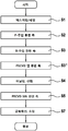
최적화된 도펀트 부가(application)는 개선된 도핑 기법, 예를 들어서, 이온 주입을 사용함에 있다. 이 방법은 반도체 기판 내로의 도펀트들의 일측면 부가(one-sided application) 또는 반도체 기판의 양측 주 표면들 내로의 상이한 도펀트들의 부가를 가능하게 한다. 양측형 도핑된 태양 전지를 생성하기 위한 흐름도가 도 1에 도시된다. 이 도면은 자체적으로 설명을 하고(self-explanatory) 있기 때문에, 보다 세부적인 설명은 필요 없다. 이러한 경우에, S2 및 S3 단계들에서의 이온 주입 이후에, 어닐링 또는 경화 단계(S4)가 이어지며, 추가적으로 얇은 산화물 층이 웨이퍼 표면 상에 성장한다. 상기 산화물 층은 이후의 단계들(S5 또는 S6)에서 증착된 SiN 캡(cap)과 함께 패시베이션 스택(passivation stack)을 형성한다.
본 발명자들의 실험들은 실제 응용이 문제가 있었다고 보였다. 이러한 방법으로 생성된 태양 전지들의 효율은 보다 복잡한 공정으로 제조된 태양 전지들에 매우 크게 의존한다.
이는 다른 이유들 중에서도 다음과 같은 효과들로 인한 것이다: 주입된 붕소 이미터의 경화는 불활성 분위기에서 매우 높은 온도(>1000 ℃)에서의 어닐링 단계를 요구하기 때문이다. 이러한 조건들은 인 BSF(Back Surface Field)의 경화에 있어서 이상적이지 않다. 인은 높은 온도로 인해서 기판 내로 매우 깊게 확산된다. 이는 태양 전지의 양자 효율을 저하시키는 증가된 자유-캐리어-흡수(Free-Carrier-Absorption)로 이어진다. 또한, 표면 근처에 있는 인들은 기화된다. 이러한 도핑제 손실은 태양 전지의 후면 측에서의 접촉 저항을 증가시키고 이미터 및 BSF 간에 단락을 초래하며 이는 이른바 자동도핑(autodoping)으로 이어진다.
본 발명은 청구항 제1항의 특징들을 갖는 방법을 제공한다. 본 발명의 개념의 적합한 실시예들은 종속항들의 대상이다.
본 발명의 목적은 전술한 인 도핑 영역의 부정적인 영향들을 적어도 제한하거나 및/또는 보상하기 위해서 어닐링 단계(고온 경화) 수행 이전에 예방적 조치를 취하는 것이다. 따라서, 제 2 표면 상에, 제 2 도펀트에 대한 외부확산 베리어 역할을 하는 캡들을 증착하는 것이 제안된다.
이로써, 본 발명은 BSF 주입 이후에 그리고 경화 단계 이전에 태양 전지의 후면 측 상에 캡을 증착함으로써 전술한 문제를 해결하게 한다. 산소가 침투할 수 없는 캡이 또한 일 실시예에서 사용되어서 태양 전지의 후면 측 상에서의 이른바 산화-증진된-확산(oxidation-enhanced-diffusion: OED)을 방지할 수 있다. 이러한 수단들로 인해서, BSF-프로파일은 상술한 단점들을 가지지 않게 된다. 마찬가지로, 적합한 마스킹이 자동도핑을 방지할 수 있다. 다른 실시예에서, 어닐링 단계 동안에 규소 내에 베이컨시들(vacancies)을 주입하는 층이 증착될 수 있다. 이러한 베이컨시들은 인의 확산을 더 저하시킬 것이다. 본 프로세스는 인장 응력을 받는 피복 층 및/또는 아화학양론적 피복 층(substoichiometric covering layer)을 수반할 수 있다.
이러한 관점에서 바람직한 본 실시예에서, 제 2 표면 상에 부가된 캡은 제 2 표면 상에서 태양 전지 또는 태양 전지의 일부의 반사방지/패시베이션 층으로서 남는다. 이로써, 프로세스가 추가적으로 복잡해지지 않는다.
여기에서 문제가 되는 타입의 일 층(특히, PECVD에 의해서 형성된 층)은 후속하는 고온 단계들 중 한 단계 동안에 패시베이션 특성들의 측면에서 열화될 것이며 이로써 패시베이션 층으로서 대체적으로 사용불가능하게 될 것이라는 통상적인 가설때문에 이러한 구현가능성은 상당히 놀라운 것이다.
다른 실시예에서는, 제 2 표면에 부가된 캡은 어닐링 단계 이후에 에칭-백(etching-back)된다. 이 실시예에서, 특정 패시베이션 층이 이러한 에칭-백 이후에 다시 부가된다.
전술한 바와 같이, 다른 구성에서는, 제 2 표면 상에 부가된 캡은 PECVD 방법에 의해서 증착된다. 이와 달리, 캡을 생성하기 위해 PVD 또는 APCVD 또는 유사한 방법들이 사용될 수 있다. 본 기술 분야의 당업자는 본 방법에 따른 보다 구체적인 실시예를 후속하는 구체적인 층의 재료 파라미터들로부터 그리고 열적 단계의 파라미터들로부터, 제 2 도펀트의 도핑 파라미터들을 고려하여서, 보다 세부적인 설명을 요구하지 않으면서, 도출할 수 있다.
예시적인 실시예들의 세부사항들이 이하에서 언급된다.
재료 측면에서 바람직한 실시예들에서, 제 2 표면에 부가된 캡은 산화규소 및/또는 질화규소 층 및/또는 질화산화규소(silicon nitride oxide) 층을 포함한다. 캡은 또한 몇 개의 부분 층들을 포함하며 이 몇 개의 부분 층들 중 적어도 한 층은 질화규소 층으로서 형성되도록 설계될 수 있다.
상술한 본 발명은 규소가 반도체 재료로서 사용되는 요즘의 태양 전지들에 대해서 매우 적합하며, 붕소, 인듐, 갈륨, 알루미늄을 포함하는 그룹으로부터 선택된 원소, 특히 붕소가 제 1 도펀트로서 사용되고, 인, 비소, 안티몬을 포함하는 그룹으로부터 선택된 원소, 특히 인이 제 2 도펀트로서 사용된다. 보다 구체적으로, 본 발명자들은 본원에서 제 1 도핑 영역이 n-규소 기판의 전면 표면 내의 이미터 영역으로서 형성되고, 제 2 도핑 영역이 n-규소 기판의 후면 표면 내의 후면 표면 필드부(BSF)로서 형성되는 태양 전지들을 다루고 있다.
특히, 이러한 재료/도펀트들 구성에서, 어닐링 단계는 중성 또는 산화 분위기 내에서 850 ℃ 내지 1100 ℃ 범위의 온도에서의 경화 단계를 포함한다. 기본적으로, 다른 프로세스 분위기(가능하게는 도펀트들을 포함하는 분위기)와 함께, 주로 확산 단계들로서 설계된 열적 프로세스 단계들을 사용하여서도 캡을 제공하는 것이 본 발명에 따라서 적절하다고 입증될 수 있다.
본 발명은 첨부된 도식적 도면들을 참조하여서 예시적인 실시예를 사용하여서 이하에서 보다 세부적으로 기술될 것이다.
도 1은 결정질 태양 전지를 생성하기 위한 기존의 방법의 도식적 흐름도를 도시한다.
도 2a 및 도 2b는 본 발명에 따른 방법의 2개의 실시예들의 도면을 도시한다.
도 3a 내지 도 3e는 예시적으로 실시예의 상이한 단계들부터 생성된 규소 기판 또는 규소 기판으로부터 생성된 태양 전지의 단면도들을 도시한다.
도 1은 결정질 태양 전지를 생성하기 위한 기존의 방법의 도식적 흐름도를 도시한다.
도 2a 및 도 2b는 본 발명에 따른 방법의 2개의 실시예들의 도면을 도시한다.
도 3a 내지 도 3e는 예시적으로 실시예의 상이한 단계들부터 생성된 규소 기판 또는 규소 기판으로부터 생성된 태양 전지의 단면도들을 도시한다.
도 2a는 본 발명에 따른 방법의 일 실시예에서 결정질 태양 전지의 생성의 중요한 단계들을 흐름도로 도시적으로 도시하며, 도면 자체적으로 잘 설명을 하고 있다. 도 1에 도시된 종래 프로세스에 비해서, 기판의 후면 측 내로 인을 주입하고 기판의 전면 측 내로 붕소를 주입하는 단계들(S3) 이후의 PECVD(단계(S3+))에 의해서 기판의 후면 측 상에 캡이 제공되고, 표준 시퀀스에 있어서 이후에 기판 표면의 산화와 연관된 어닐링(단계(S4))이 따른다. 단계(S3+)에서 생성된 캡은 기판 상에서 반사방지/패시베이션 층으로서 잔류하며, 이로써 표준 프로세스 시퀀스의 단계(S6)는 본 방법에서 생략가능하다.
이와 대조하여서, 도 2b에서 도시된 시퀀스에서는 단계(S3+)에서 기판의 후면 측 상의 캡이 생성되고, 이 캡이 어닐링 단계(S4) 이후의 추가 단계(S4+)에서 다시 제거되고, 표준 프로세스 시퀀스에서, SiN 반사방지/패시베이션 층이 PECVD에 의해서 기판의 후면 측 상으로 다시 부가될 것이다. 한편, 기판의 전면 측 상에 작용방식이 유사한 층을 생성하는 단계(S5')가, 알루미늄 산화물/질화규소 층 구조체가 SiN 층 대신에 기판의 전면 측 상으로 부가되도록 적합하게 수정된다.
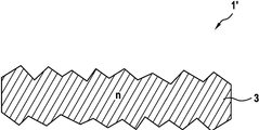
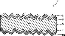
도 3a 내지 도 3e는 본 발명에 따른 방법에 의해서 생성된 태양 전지의 구성 및 그들의 생성의 중요한 국면들을 도식적 단면 표현들을 도시하고 있으며, 도 3e는 본 명세서에서 해당 프로세스 시퀀스에 의해서 생성된 태양 전지(1)를 도시한다.
도 3e는 n-타입의 결정질 규소 기판(3) 및 각각의 피라미드형 구조를 갖는 제 1(전면 측) 표면(3a) 및 제 2(후면 측) 표면(3b)을 갖는 태양 전지(1)를 단면 표현으로 도시적으로 보여준다. 제 1 표면(3a)에서, 제 1 도핑 영역(이미터 영역)(5)은 붕소 확산에 의해서 형성되고, 제 2 표면에서, 편평한 BSF(Back Surface Field)(7)가 인 주입 및 후속하는 경화/활성화에 의해서 제 2 도핑 영역으로서 형성된다. 열적 산화규소 층(8)은 경화/활성화 단계(어닐링 단계) 동안에 전면 측 상에서 볼 수 있다.
두꺼운 질화규소 층(9a 또는 9b)은 제 1 표면 및 제 2 표면(3a, 3b) 상에 반사방지 층으로서 체계적으로 증착된다. 이 반사방지 층은 산화물(예를 들어서 산화규소) 외측에서 추가 부분 층으로서 더해질 수 있으며, 층의 패시베이션 특성들을 개선시킨다. 하지만 도면에서는 도시되지 않는다. 태양 전지들의 전면 측(제 1 표면)(3a)은 전면 측 금속배선(11a)을 보이며, 태양 전지들의 후면 측(제 2 표면)(3b)은 후면 측 금속배선(11b)을 보인다.
도 3a는 프로세스 단계 S1 이후에 양 측면들 상에 텍스처링되고(textured) 세정된 n-규소 기판(1')을 도식적으로 도시하며; 도 3b는 프로세스 단계(S3) 이후의 전면 측 (초기) 붕소 주입 영역(5') 및 후면 측 인 주입 영역(7')을 갖는 텍스처링된 태양 전지 기판(1')을 도시하며; 도 3c는 단계(S3+)에서의 후면 측 캡(9b)의 증착 이후의 상황을 도시하며; 그리고, 도 3d는 어닐링 단계(S4) 이후의 상황을 도시하며, 여기서 양 도핑 영역들(5, 7)은 깊이 방향으로 확장되며, 열적 산화물(8)은 전면 표면 상에서 성장한다.
본 발명자들은 이제 주요 프로세스 단계들에 대한 상술된 간략한 설명에 코멘트 및 조언들을 해서 변형사항들 및 대체사항들을 설명한다.
S1
:
텍스처링
/세정
본 프로세스 단계는 후속하는 세정과 산업 표준 텍스처링을 함께 수반한다. 선택사양적으로, 웨이퍼는 후면 측이 계획될 수 있다. 이를 위해서, 몇몇 방법들이 본 기술 분야의 최신 방법에 의해서 제공되며, 본 발명에 있어서는 중요하지 않다.
S2
: 붕소 주입
태양 전지의 전면 측 내로의 붕소의 주입이 수행되는데, 예를 들어서 0.5 내지 5el5 1/cm2 의 도즈량(dose) 및 1-40 keV의 에너지로, 바람직하게는 1.5 내지 3el5 1/cm2의 도즈량 및 3-10 keV의 에너지로 수행된다. 붕소 층의 층 저항은 경화 후에 30 내지 300 Ohm/sqare; 바람직하게는 60-100 Ohm/sqare이다. 다른 실시예에서, 이러한 주입은 도즈량이 금속배선 영역(metallisation region) 아래에서 보다 높게 되도록 선택적일 수 있다.
이러한 붕소 주입은 또한 후면 측 캡의 증착 이후에(단계(S3+)와 단계(S4) 간에) 발생할 수도 있다. 이는 캡 증착 동안에 주입된 영역의 임의의 기계적 손상을 방지하도록 유리하다고 입증될 수 있다.
S3
: 인 주입
여기에서, 인은 태양 전지의 후면 측 내로 주입된다(예를 들어서 0.5 내지 5el5 1/cm2 의 도즈량 및 1-40 keV의 에너지로, 바람직하게는 2.5 내지 4el5 1/cm2의 도즈량 및 10 keV의 에너지로 수행됨). 인 층의 층 저항은 경화 후에 10 내지 300 Ohm/square; 바람직하게는 30-120 Ohm/square이다. 다른 실시예에서, 이러한 주입은 도즈량이 금속배선 영역 아래에서 보다 높게 되도록 선택적일 수 있다.
S3
+: 후면 측 상의 캡
후면 측 상의 캡은 인의 외부확산을 방지하고 선택사양적으로 산소의 내부확산을 방지한다. 도 2a에 따른 변형 실시예에서, 캡은 태양 전지 상에서 잔류하여서 후면 측 상의 패시베이션 층으로서 사용된다.
가장 간단한 실시예에서, 캡은 순수한 SiO2(n=1.4 내지 1.6, 바람직하게는n=1.46) 또는 순수한 SiN 층(n=1.8 내지 2.2, 바람직하게는 1.9 내지 2)이다. 선택사양적으로, 산소 및 질소 함량의 편차를 조절함으로써 이상적인 패시베이션 및 산소에 대한 침투성을 획득하도록 SiON의 사용이 가능하다(n = 1.46 내지 2.2). 이 층의 두께는 1 nm 내지 250 nm, 바람직하게는 30 내지 80 nm의 범위에 있는다.
정상적으로는, 캡 층은 SiH4, N2O/O2/CO2, NH3, N2, Ar을 포함하는 그룹으로부터 선택된 하나 또는 몇 개의 가스들로부터 선택된 화학물질을 사용하여서 PECVD 프로세스에 의해서 증착된다. 증착 프로세스로 인해서, 층들은 15 % 이하의 수분 함량을 갖는데 이는 어닐링 단계(5)로 인한 것이다. 이와 달리, 캡 층은 예를 들어서, APCVD 또는 PVD와 같은 다른 방법들을 사용하여서 부가될 수 있다.
모든 요건들의 최적화를 위해서, 층 스택이 사용될 수 있는데, 예를 들어서, SiO2/SiN2 층 스택 또는 서로 상이한 굴절율들을 갖는 2 개의 SiN 층들로 구성된 층일 수 있다. 이 프로세스의 성공여부는 후면 측 캡의 부가에 크게 의존한다.
캡 증착 이후에 최적 세정 단계가 이어질 수 있으며 이는 임의의 입자들 및 가능한 오염물을 제거하기 위한 것이다. 세정은 하나 이상의 프로세스 화학물질들 HF, HCl, H2O2을 사용하여서 수분 기반 욕 내에서 습식-화학적으로 수행될 수 있다.
S4:
어닐링
열적 후처리 단계는 주입 손상부들을 경화시키고, 주입된 도펀트들을 활성화시키고, 이미터 및 BSF의 목표 깊이를 획득하기 위해서 붕소 및 인을 웨이퍼 내로 확산시킨다. 어닐링 프로세스는 인보다 매우 크리티컬한(critical) 붕소를 활성화시키기는 요건들에 달려있다. 붕소 활성화는 정상적으로는 불활성 분위기(N2,Ar) 내에서 고온(900 내지 1100 ℃)에서의 어닐링을 요구한다. 발생 순서에 따른 부분적인 단계들에서, 산소가 주입되어서 웨이퍼 표면 상에서 산화물 층을 성장시키고 OED 효과를 통해서 붕소 확산을 가속화시킬 수 있다. 어닐링 프로세스는 5 내지 300 분 동안 지속되며, 바람직하게는 15 내지 60 분 동안 지속된다. 어닐링 프로세스 동안에 성장한 산화물 층은 후속하는 패시베이션을 가능하게 하며, 그의 두께는 1 내지 150nm, 바람직하게는 5 내지 25nm 범위에 있다. 확산 영역들의 깊이들은 30 내지 2500nm, 바람직하게는 400 내지 1000nm 범위에 있다.
이와 달리, RTA(Rapid Thermal Anneal) 단계가 고려될 수 있는데, 이 단계 동안에 태양 전지는 매우 고온(1000 ℃ 이상)에서의 매우 짧은 시간 동안에 가열될 수 있다.
S5
: 전면 측
패시베이션
가장 간단한 실시예에서, 태양 전지의 전면 측 패시베이션은 SiO/SiN을 사용하여 수행된다. 이를 위해서, 단계(S4)의 열적으로 성장한 산화규소(SiO2)가 사용된다. SiN이 PECVD 프로세스를 통해서 증착된다. 본 변형은 프로세스의 저 비용으로 인해서 유리하다. SiN은 정상적으로는 1.98 내지 2.15(바람직하게는 2.05)의 굴절율을 가지며, 10 내지 150nm(바람직하게는 60 내지 90nm)의 두께로 증착된다.
이와 달리, AI2O3/SiN 층 스택이 전면 측 패시베이션을 위해서 사용될 수 있다. 이를 위해서, 전면 측 상의 SiO2는 선택적으로 제거되어야 한다. 이는 예를 들어서 HF를 사용하는 습식 에칭 단계를 수반할 수 있다.
S7: 금속배선(
metallisation
)
금속배선은 표준 산업 방법들을 사용할 수 있으며 본 발명에 있어서는 중요하지 않다. 전면 측 금속배선이 정상적으로는 은 그리드(silver grid)를 사용하여서 수행되고, 후면 측 금속배선은 또한 은 그리드를 사용하여서 수행되거나, 예를 들어서 레이저 어블레이션(laser ablation) 및 PVD에 의해서 생성된 국부적 컨택트들을 갖는 전체 표면 알루미늄 금속배선을 사용하여서 수행된다.
본 기술 분야의 당업자에게 알려진 보다 특정화된 맥락에서, 다른 실시예들 및 변형들이 전적으로 예시적으로 본 명세서에서 도시된 방법 및 디바이스에 기초하여서 고려될 수 있다. 본 발명은 예를 들어서, MWT-nPERT 태양 전지들, p-타입 PERT 태양 전지들 등과 같은, 붕소 및 인 주입을 갖는 다른 태양 전지 개념에 대해서도 사용될 수 있다는 것이 염두되어야 한다.
Claims (11)
- 결정질 반도체 재료로부터 태양 전지(1)를 생성하는 방법으로서, 반도체 기판(3)의 제 1 표면(3a)에 제 1 도펀트의 이온 주입(S2)에 의해 제 1 도핑 영역(5)이 형성되고, 상기 반도체 기판의 제 2 표면(3b)에 제 2 도펀트의 이온 주입(S3) 또는 열적 내부확산에 의해 제 2 도핑 영역(7)이 형성되며, 상기 제 2 표면의 도핑 이후에, 제 2 도펀트에 대해서 외부확산 베리어로 작용하는 캡(9b)이 상기 제 2 표면 상에 부가되며, 이후에 어닐링 단계(S4)가 수행되는, 태양 전지 생성 방법.
- 제1항에 있어서,
상기 제 2 표면(3b) 상에 부가된 캡(9b)은 캡의 조성(composition), 성질(nature) 및 두께로 인해서 산소가 침투할 수 없도록 형성되는, 태양 전지 생성 방법. - 제1항 또는 제2항에 있어서,
상기 제 2 표면(3b) 상에 부가된 캡(9b)은 제 2 표면 상에서 상기 태양 전지(1) 또는 태양 전지의 일부의 반사방지/패시베이션 층으로서 잔류하는, 태양 전지 생성 방법. - 제1항 또는 제2항에 있어서,
상기 제 2 표면(3b) 상에 부가된 캡(9b)은 상기 어닐링 단계(S4) 이후에 에칭 백(etched back)되는, 태양 전지 생성 방법. - 제1항 내지 제4항 중 어느 한 항에 있어서,
상기 제 2 표면(3b) 상에 부가된 캡(9b)은 PECVD 프로세스(S4)에 의해서 증착되는, 태양 전지 생성 방법. - 제1항 내지 제5항 중 어느 한 항에 있어서,
상기 제 2 표면(3b) 상에 부가된 캡(9b)은, 산화규소 층, 질화규소 층 및 질화산화규소(silicon oxide nitride) 층 중 하나 이상을 포함하는, 태양 전지 생성 방법. - 제6항에 있어서,
상기 캡(9b)은 복수의 부분 층들을 포함하며, 상기 부분 층들 중 적어도 하나는 질화규소 층으로 형성되는, 태양 전지 생성 방법. - 제1항 내지 제7항 중 어느 한 항에 있어서,
상기 캡(9b)은 상기 제 1 표면(3a) 내로 제 1 도펀트를 이온 주입하기 전에 형성되는, 태양 전지 생성 방법. - 제1항 내지 제8항 중 어느 한 항에 있어서,
상기 반도체 재료는 규소일 수 있으며, 상기 제 1 도펀트는 붕소, 인듐, 갈륨, 알루미늄를 포함하는 그룹으로부터 선택된 원소일 수 있으며, 특히 붕소이고, 상기 제 2 도펀트는 인, 비소, 안티몬을 포함하는 그룹으로부터 선택된 원소일 수 있으며, 특히 인(phosphorus)인, 태양 전지 생성 방법. - 제1항 내지 제9항 중 어느 한 항에 있어서,
상기 제 1 도핑 영역은 n-규소 기판(3)의 전면 표면(3a) 내의 이미터 영역으로서 형성되고, 상기 제 2 도핑 영역은 상기 n-규소 기판의 후면 표면(3b)에서 후면 표면 필드부(7)로서 형성되는, 태양 전지 생성 방법. - 제1항 내지 제10항 중 어느 한 항에 있어서,
상기 어닐링 단계(S4)는 850 ℃ 내지 1100 ℃ 범위의 온도에서 중성 또는 산화 분위기에서의 경화 단계를 포함하는, 태양 전지 생성 방법.
Applications Claiming Priority (3)
| Application Number | Priority Date | Filing Date | Title |
|---|---|---|---|
| DE102013218351.8 | 2013-09-13 | ||
| DE102013218351.8A DE102013218351A1 (de) | 2013-09-13 | 2013-09-13 | Verfahren zur Herstellung einer Solarzelle |
| PCT/EP2014/066856 WO2015036181A1 (de) | 2013-09-13 | 2014-08-05 | Verfahren zur herstellung einer solarzelle umfassend eine dotierung durch ionenimplantation und abscheiden einer ausdiffusionsbarriere |
Publications (1)
| Publication Number | Publication Date |
|---|---|
| KR20160071373A true KR20160071373A (ko) | 2016-06-21 |
Family
ID=51383707
Family Applications (1)
| Application Number | Title | Priority Date | Filing Date |
|---|---|---|---|
| KR1020167008592A KR20160071373A (ko) | 2013-09-13 | 2014-08-05 | 이온 주입에 의한 도핑 및 외부확산 베리어 증착을 포함하는 태양 전지 생성 방법 |
Country Status (8)
| Country | Link |
|---|---|
| US (1) | US10263135B2 (ko) |
| EP (1) | EP3044813A1 (ko) |
| JP (1) | JP2016535457A (ko) |
| KR (1) | KR20160071373A (ko) |
| CN (1) | CN106104755A (ko) |
| DE (1) | DE102013218351A1 (ko) |
| MY (1) | MY173528A (ko) |
| WO (1) | WO2015036181A1 (ko) |
Families Citing this family (6)
| Publication number | Priority date | Publication date | Assignee | Title |
|---|---|---|---|---|
| KR101680036B1 (ko) * | 2015-07-07 | 2016-12-12 | 엘지전자 주식회사 | 태양 전지 및 이의 제조 방법 |
| WO2017072758A1 (en) | 2015-10-25 | 2017-05-04 | Solaround Ltd. | Method of bifacial cell fabrication |
| DE102016125316B4 (de) * | 2016-12-22 | 2021-07-22 | Infineon Technologies Austria Ag | Herstellen von rekombinationszentren in einem halbleiterbauelement |
| CN107425086A (zh) * | 2017-05-18 | 2017-12-01 | 阳光中科(福建)能源股份有限公司 | 一种离子注入法制作n型pert双面太阳电池的制备工艺 |
| DE102019104249A1 (de) * | 2019-02-20 | 2020-08-20 | Hanwha Q Cells Gmbh | Verfahren zur Herstellung einer PERC-Solarzelle und PERC-Solarzelle |
| CN111640804A (zh) * | 2020-06-01 | 2020-09-08 | 国家电投集团西安太阳能电力有限公司 | 一种氧化硅/氮化硅叠层膜的n-pert双面电池结构 |
Family Cites Families (21)
| Publication number | Priority date | Publication date | Assignee | Title |
|---|---|---|---|---|
| JPS5363993A (en) * | 1976-11-19 | 1978-06-07 | Matsushita Electric Ind Co Ltd | Production of semiconductor device |
| DE3340874A1 (de) | 1983-11-11 | 1985-05-23 | Telefunken electronic GmbH, 7100 Heilbronn | Verfahren zum herstellen einer solarzelle |
| JP2003152205A (ja) * | 2001-11-12 | 2003-05-23 | Sharp Corp | 光電変換素子及びその製造方法 |
| JP2004193350A (ja) * | 2002-12-11 | 2004-07-08 | Sharp Corp | 太陽電池セルおよびその製造方法 |
| JP4632672B2 (ja) * | 2004-02-04 | 2011-02-16 | シャープ株式会社 | 太陽電池の製造方法 |
| US7144751B2 (en) * | 2004-02-05 | 2006-12-05 | Advent Solar, Inc. | Back-contact solar cells and methods for fabrication |
| US20050172996A1 (en) * | 2004-02-05 | 2005-08-11 | Advent Solar, Inc. | Contact fabrication of emitter wrap-through back contact silicon solar cells |
| US20060060238A1 (en) * | 2004-02-05 | 2006-03-23 | Advent Solar, Inc. | Process and fabrication methods for emitter wrap through back contact solar cells |
| JP4849786B2 (ja) * | 2004-08-30 | 2012-01-11 | シャープ株式会社 | 多接合型化合物太陽電池およびその製造方法 |
| JP2006310389A (ja) * | 2005-04-26 | 2006-11-09 | Sharp Corp | 太陽電池の製造方法 |
| US9318644B2 (en) * | 2009-05-05 | 2016-04-19 | Solexel, Inc. | Ion implantation and annealing for thin film crystalline solar cells |
| DE102010003784A1 (de) * | 2010-04-09 | 2011-10-13 | Robert Bosch Gmbh | Verfahren zur Herstellung einer Solarzelle |
| EP2490268A1 (en) * | 2011-02-03 | 2012-08-22 | Imec | Method for fabricating photovoltaic cells |
| EP2805334A4 (en) | 2012-01-16 | 2015-10-28 | Heraeus Precious Metals North America Conshohocken Llc | ALUMINUM CONDUCTIVE PASTE FOR CELLS ON REAR SIDE WITH PASSIVATED SURFACE WITH LOCALLY OPEN METALLIC HOLES. |
| JP2013165160A (ja) * | 2012-02-10 | 2013-08-22 | Shin Etsu Chem Co Ltd | 太陽電池の製造方法及び太陽電池 |
| US9330917B2 (en) * | 2012-02-24 | 2016-05-03 | Varian Semiconductor Equipment Associates, Inc. | Passivation layer for workpieces formed from a polymer |
| KR101872786B1 (ko) * | 2012-06-22 | 2018-06-29 | 엘지전자 주식회사 | 태양 전지의 불순물층 형성 방법 및 태양 전지의 제조 방법 |
| CN102856436A (zh) * | 2012-09-05 | 2013-01-02 | 友达光电股份有限公司 | 太阳能电池及其制作方法 |
| DE102012217078B4 (de) * | 2012-09-21 | 2015-03-05 | Fraunhofer-Gesellschaft zur Förderung der angewandten Forschung e.V. | Verfahren zum Herstellen einer photovoltaischen Solarzelle |
| US9515217B2 (en) * | 2012-11-05 | 2016-12-06 | Solexel, Inc. | Monolithically isled back contact back junction solar cells |
| US20140261666A1 (en) * | 2013-03-13 | 2014-09-18 | Applied Materials, Inc. | Methods of manufacturing a low cost solar cell device |
-
2013
- 2013-09-13 DE DE102013218351.8A patent/DE102013218351A1/de not_active Withdrawn
-
2014
- 2014-08-05 US US15/021,077 patent/US10263135B2/en active Active
- 2014-08-05 JP JP2016541855A patent/JP2016535457A/ja active Pending
- 2014-08-05 KR KR1020167008592A patent/KR20160071373A/ko not_active Application Discontinuation
- 2014-08-05 CN CN201480058077.2A patent/CN106104755A/zh active Pending
- 2014-08-05 WO PCT/EP2014/066856 patent/WO2015036181A1/de active Application Filing
- 2014-08-05 EP EP14753037.2A patent/EP3044813A1/de not_active Withdrawn
- 2014-08-05 MY MYPI2016700869A patent/MY173528A/en unknown
Also Published As
| Publication number | Publication date |
|---|---|
| MY173528A (en) | 2020-01-31 |
| DE102013218351A1 (de) | 2015-03-19 |
| CN106104755A (zh) | 2016-11-09 |
| WO2015036181A1 (de) | 2015-03-19 |
| US20160233372A1 (en) | 2016-08-11 |
| EP3044813A1 (de) | 2016-07-20 |
| JP2016535457A (ja) | 2016-11-10 |
| US10263135B2 (en) | 2019-04-16 |
Similar Documents
| Publication | Publication Date | Title |
|---|---|---|
| CN107195699B (zh) | 一种钝化接触太阳能电池及制备方法 | |
| KR20160071373A (ko) | 이온 주입에 의한 도핑 및 외부확산 베리어 증착을 포함하는 태양 전지 생성 방법 | |
| US20200279970A1 (en) | Method of Manufacturing a Passivated Solar Cell and Resulting Passivated Solar Cell | |
| JP6392385B2 (ja) | 太陽電池の製造方法 | |
| KR101872786B1 (ko) | 태양 전지의 불순물층 형성 방법 및 태양 전지의 제조 방법 | |
| CN110838536A (zh) | 具有多种隧道结结构的背接触太阳能电池及其制备方法 | |
| WO2010055346A3 (en) | Deep grooved rear contact photovoltaic solar cells | |
| WO2012027000A3 (en) | Back junction solar cell with selective front surface field | |
| US20130089942A1 (en) | Method for producing a solar cell | |
| TW201208104A (en) | Ion implanted selective emitter solar cells with in situ surface passivation | |
| CN111354838B (zh) | 太阳能电池及其制备方法、n型掺杂硅膜的处理方法 | |
| CN110943143A (zh) | 用于制造具有异质结和发射极扩散区的光伏太阳能电池的方法 | |
| KR102320551B1 (ko) | 태양 전지의 제조 방법 | |
| JP5830147B1 (ja) | 太陽電池及び太陽電池の製造方法 | |
| US20160240724A1 (en) | Method for producing a solar cell | |
| Lanterne et al. | Annealing, passivation and contacting of ion implanted phosphorus emitter solar cells | |
| CN111149217A (zh) | 界面特性得到提升的钝化发射极背面接触(perc)太阳能电池制造方法以及制造装置 | |
| Ghembaza et al. | Efficiency improvement of crystalline silicon solar cells by optimizing the doping profile of POCl3 diffusion | |
| CN103730541B (zh) | 太阳能电池纳米发射极及其制备方法 | |
| CN112466996B (zh) | 太阳能电池及形成方法 | |
| NL2021449B1 (en) | A method of manufacturing a passivated solar cell and resulting passivated solar cell | |
| CN102122683A (zh) | 采用腐蚀浆料法制备单晶硅太阳能电池选择发射极的工艺 | |
| KR101161210B1 (ko) | 태양전지의 에미터 형성방법 | |
| CN110870082A (zh) | 用于制造pert太阳能电池的方法 | |
| KR102106071B1 (ko) | 태양전지의 제조 방법 |
Legal Events
| Date | Code | Title | Description |
|---|---|---|---|
| A201 | Request for examination | ||
| E902 | Notification of reason for refusal | ||
| E601 | Decision to refuse application |