KR20150103577A - Device handler and method for handling device - Google Patents
Device handler and method for handling device Download PDFInfo
- Publication number
- KR20150103577A KR20150103577A KR1020140025178A KR20140025178A KR20150103577A KR 20150103577 A KR20150103577 A KR 20150103577A KR 1020140025178 A KR1020140025178 A KR 1020140025178A KR 20140025178 A KR20140025178 A KR 20140025178A KR 20150103577 A KR20150103577 A KR 20150103577A
- Authority
- KR
- South Korea
- Prior art keywords
- image
- wafer ring
- transfer tool
- elements
- axis direction
- Prior art date
Links
Images


Classifications
-
- G—PHYSICS
- G01—MEASURING; TESTING
- G01R—MEASURING ELECTRIC VARIABLES; MEASURING MAGNETIC VARIABLES
- G01R31/00—Arrangements for testing electric properties; Arrangements for locating electric faults; Arrangements for electrical testing characterised by what is being tested not provided for elsewhere
- G01R31/26—Testing of individual semiconductor devices
- G01R31/2601—Apparatus or methods therefor
-
- H—ELECTRICITY
- H01—ELECTRIC ELEMENTS
- H01L—SEMICONDUCTOR DEVICES NOT COVERED BY CLASS H10
- H01L21/00—Processes or apparatus adapted for the manufacture or treatment of semiconductor or solid state devices or of parts thereof
- H01L21/67—Apparatus specially adapted for handling semiconductor or electric solid state devices during manufacture or treatment thereof; Apparatus specially adapted for handling wafers during manufacture or treatment of semiconductor or electric solid state devices or components ; Apparatus not specifically provided for elsewhere
- H01L21/673—Apparatus specially adapted for handling semiconductor or electric solid state devices during manufacture or treatment thereof; Apparatus specially adapted for handling wafers during manufacture or treatment of semiconductor or electric solid state devices or components ; Apparatus not specifically provided for elsewhere using specially adapted carriers or holders; Fixing the workpieces on such carriers or holders
- H01L21/67333—Trays for chips
-
- H—ELECTRICITY
- H01—ELECTRIC ELEMENTS
- H01L—SEMICONDUCTOR DEVICES NOT COVERED BY CLASS H10
- H01L21/00—Processes or apparatus adapted for the manufacture or treatment of semiconductor or solid state devices or of parts thereof
- H01L21/67—Apparatus specially adapted for handling semiconductor or electric solid state devices during manufacture or treatment thereof; Apparatus specially adapted for handling wafers during manufacture or treatment of semiconductor or electric solid state devices or components ; Apparatus not specifically provided for elsewhere
- H01L21/677—Apparatus specially adapted for handling semiconductor or electric solid state devices during manufacture or treatment thereof; Apparatus specially adapted for handling wafers during manufacture or treatment of semiconductor or electric solid state devices or components ; Apparatus not specifically provided for elsewhere for conveying, e.g. between different workstations
-
- H—ELECTRICITY
- H01—ELECTRIC ELEMENTS
- H01L—SEMICONDUCTOR DEVICES NOT COVERED BY CLASS H10
- H01L21/00—Processes or apparatus adapted for the manufacture or treatment of semiconductor or solid state devices or of parts thereof
- H01L21/67—Apparatus specially adapted for handling semiconductor or electric solid state devices during manufacture or treatment thereof; Apparatus specially adapted for handling wafers during manufacture or treatment of semiconductor or electric solid state devices or components ; Apparatus not specifically provided for elsewhere
- H01L21/68—Apparatus specially adapted for handling semiconductor or electric solid state devices during manufacture or treatment thereof; Apparatus specially adapted for handling wafers during manufacture or treatment of semiconductor or electric solid state devices or components ; Apparatus not specifically provided for elsewhere for positioning, orientation or alignment
-
- H—ELECTRICITY
- H01—ELECTRIC ELEMENTS
- H01L—SEMICONDUCTOR DEVICES NOT COVERED BY CLASS H10
- H01L22/00—Testing or measuring during manufacture or treatment; Reliability measurements, i.e. testing of parts without further processing to modify the parts as such; Structural arrangements therefor
- H01L22/30—Structural arrangements specially adapted for testing or measuring during manufacture or treatment, or specially adapted for reliability measurements
Abstract
Description
본 발명은 소자핸들러에 관한 것으로서, 보다 상세하게는 반도체공정 및 소잉공정을 마친 소자들을 웨이퍼로부터 픽업하여 언로딩하는 소자핸들러 및 소자핸들링방법에 관한 것이다.BACKGROUND OF THE
SD 램, 프래쉬램, LSI, LED 등 반도체소자(이하 '소자'라 한다)는 반도체공정을 마친 후 소잉공정, 패키징공정 등을 마친 후 시장에 출하됨이 일반적이다.Semiconductor devices (hereinafter referred to as "devices") such as SD RAM, flash ram, LSI, and LED are generally shipped to the market after completion of the semiconductor process, the sowing process, and the packaging process.
그리고 시장에 출하된 제품에 대한 신뢰성을 확보하기 위하여 검사장치, 분류장치, 검사 및 분류장치 등에 의하여 자동검사 및 검사결과에 따른 분류를 통하여 양품의 제품들을 선별하여 시장에 출하하고 있다.In order to ensure the reliability of the products shipped to the market, the products of good products are selected and shipped to the market by sorting according to the automatic inspection and inspection result by inspection apparatus, sorting apparatus, inspection and sorting apparatus.
또한 소자는 SD 램, 프래쉬램, LSI 등 리드프레임, BGA 등 단자구조가 다양해지는 등 칩의 종류가 다양해지고 있다.In addition, chip types such as SDRAM, flash RAM, LSI, lead frame, BGA, etc., are becoming diverse.
최근에는 소자에 대한 소형화 및 고집적화 요구에 따라서 소자가 수지 등에 의한 몰딩공정을 거치지 않고 웨이퍼 레벨에서 최종 제품화되는 것이 확대되고 있는 추세이다.In recent years, there has been an increasing tendency that devices are made into final products at a wafer level without being subjected to a molding process using a resin or the like in accordance with the demand for miniaturization and high integration of devices.
한편 SD램, 모바일SD램, 모바일CPU와 같은 LSI와 같은 반도체 시장에서 경쟁이 격화되면서 소자제조비용의 절감될 필요가 있으며 궁극적으로 생산성을 높이는 것이 매우 절실하다.Meanwhile, as competition intensifies in semiconductor markets such as SDRAM, mobile SDRAM, and mobile CPU, it is necessary to reduce device manufacturing costs and ultimately increase productivity.
그리고 반도체 생산은 클린룸 내에서 전공정이 수행되는바 클린룸 내에서 각 공정을 수행하는 장비의 처리속도가 생산성에 직결되는바, 웨이퍼 수준에서 소자를 언로딩하는 소자핸들러 또한 장비의 처리속도를 높이는 것이 중요하다.In semiconductor manufacturing, the processing speed of the equipment that performs each process in the clean room where the process is performed in the clean room is directly related to the productivity. The device handler which unloads the device at the wafer level also increases the processing speed of the equipment It is important.
그런데 웨이퍼 수준에서 소자를 언로딩하는 소자핸들러는 반도체 공정 및 소잉공정을 마친 웨이퍼링으로부터 소자를 픽업하여 캐리어테이프와 같은 적재부재에 담아 웨이퍼링으로부터 소자를 언로딩하도록 구성된다.However, a device handler for unloading a device at the wafer level is configured to pick up the device from the wafer ring after semiconductor processing and sowing processes and to load the device from a wafer ring by placing it in a loading member such as a carrier tape.
여기서 소자핸들러의 처리속도(통상 시간당 처리개수(UPH)로 체크된다)는 웨이퍼링으로부터 소자를 픽업하여 캐리어테이프와 같은 적재부재에 소자를 플레이스하는 처리량에 의하여 결정된다.Here, the processing speed of the element handler (normally checked by the number of processing per hour (UPH)) is determined by the throughput of picking up the element from the wafer ring and placing the element in a loading member such as a carrier tape.
특히 소자핸들러의 처리속도는, 카메라에 의한 소자인식 및 웨이퍼링과 픽커와의 위치보정 등 웨이퍼링 상의 소자픽업 효율, 픽업 후 적재부재로의 소자적재 효율에 의하여 결정된다.Particularly, the processing speed of the element handler is determined by the device pickup efficiency on the wafer ring, such as device recognition by the camera and positional correction between the wafer ring and the picker, and the device loading efficiency to the post-pick-up member.
본 발명의 목적은 상기와 같은 추세 및 요구에 맞추어, 반도체공정 및 소잉공정을 마친 웨이퍼로부터 소자를 픽업하여 적재부재에 적재하는 장치의 처리속도를 현저히 높일 수 있는 소자핸들러 및 소자핸들링방법을 제공하는 데 있다.It is an object of the present invention to provide a device handler and a device handling method capable of significantly increasing the processing speed of an apparatus for picking up an element from a wafer after a semiconductor process and sowing process and stacking it on a stacking member in accordance with the above- There is.
본 발명은 상기와 같은 본 발명의 목적을 달성하기 위하여 창출된 것으로서, 본 발명은, 반도체공정 및 소잉공정을 마친 다수의 소자들이 부착된 복수의 웨이퍼링들이 적재된 웨이퍼링카세트부와; 상기 웨이퍼링카세트부로부터 웨이퍼링을 공급받아 웨이퍼링을 수평방향으로 이동하는 웨이퍼링테이블과; 상기 웨이퍼링테이블로부터 수평방향으로 이격되어 설치되며 상기 웨이퍼링으로부터 소자를 전달받아 적재하는 적재부재가 설치된 언로딩부와; 상기 웨이퍼링테이블의 상측에 설치되며 상기 웨이퍼링테이블에 안착된 웨이퍼링에 부착된 소자들의 일부에 대한 이미지를 획득하는 제1이미지획득부와; 상기 제1이미지획득부에 의하여 획득된 이미지 내에 포함된 복수의 소자들을 획득된 이미지를 이용하여 픽업위치로 이동하여 획득된 이미지 내에 포함된 복수의 소자들을 모두 픽업한 후 선형이동 및 회전이동 중 적어도 어느 하나의 이동에 의하여 상기 언로딩부의 적재부재로 소자를 전달하는 제1이송툴을 포함하는 것을 특징으로 하는 소자핸들러를 개시한다.The present invention has been made in order to achieve the above-mentioned object of the present invention, and it is an object of the present invention to provide a wafer ring cassette having a plurality of wafer rings on which a plurality of devices having completed semiconductor processing and sowing processes are mounted; A wafer ring table for receiving the wafer ring from the wafer ring cassette and moving the wafer ring horizontally; An unloading unit installed horizontally spaced apart from the wafer ring table and provided with a loading member for transferring and receiving the elements from the wafer ring; A first image acquiring unit installed on the wafer ring table and acquiring an image of a part of elements attached to the wafer ring placed on the wafer ring table; A plurality of elements included in the image acquired by the first image acquiring unit are moved to a pickup position using the acquired image to pick up all the plurality of elements included in the acquired image, And a first transfer tool for transferring the element to the loading member of the unloading portion by any one of the movements.
상기 제1이송툴은 상기 제1이미지획득부에 의하여 획득된 이미지 내에 포함된 복수의 소자들을 모두 픽업한 후 저면이 상측을 항하도록 180°회전하여 픽업된 소자들을 반전시키며, 상기 제1이송툴에 의하여 반전된 소자를 픽업한 후 선형이동 및 회전이동 중 적어도 어느 하나의 이동에 의하여 상기 언로딩부의 적재부재로 소자를 전달하는 제2이송툴을 추가로 포함할 수 있다.The first transfer tool picks up all of a plurality of elements included in the image acquired by the first image acquiring unit and then rotates 180 ° so that the bottom faces the upper side to invert the picked up elements, And a second transfer tool for transferring the element to the loading member of the unloading unit by at least one of linear movement and rotational movement after picking up the element inverted by the unloading unit.
상기 제1이송툴은, n×m배열(n은 1 이상의 자연수, m은 2 이상의 자연수)의 복수의 픽커들을 포함할 수 있다.The first transporting tool may include a plurality of pickers of an n x m arrangement (n is a natural number of 1 or more, and m is a natural number of 2 or more).
상기 제1이송툴은, 복수의 픽커들과, 상기 복수의 픽커들이 지지되어 설치되는 지지부재를 포함하며, 상기 지지부재는 상기 복수의 픽커들이 지지되는 방향에서 원형, 타원형 및 다각형 중 어느 하나의 형상을 가질 수 있다.The first transporting tool may include a plurality of pickers and a support member on which the plurality of pickers are supported, and the support member may be formed of any one of circular, elliptical, and polygonal Shape.
상기 제1이송툴은, 회전구동하는 회전모터의 회전축을 중심으로 각각 방사상으로 배치되는 복수의 픽커들을 포함할 수 있다.The first conveying tool may include a plurality of pickers radially arranged around a rotation axis of a rotating motor that rotates.
상기 제1이송툴은, 평행하게 한 쌍으로 설치되고, 상기 적재부재는 상기 한 쌍의 제1이송툴이 이루는 평행한 방향과 수직방향으로 이동될 수 있다.The first transfer tool is installed in a pair in parallel, and the loading member can be moved in a direction perpendicular to the parallel direction of the pair of first transfer tools.
상기 소자핸들러는 소자들이 상기 제1이송툴에 의하여 상기 언로딩부의 적재부재로 전달될 때 상기 제1이송툴에 의하여 픽업된 소자의 저면에 대한 비전검사를 위하여 소자의 저면에 대한 이미지를 획득하는 제2이미지획득부를 추가로 포함할 수 있다.The device handler obtains an image of the bottom surface of the device for vision inspection of the bottom surface of the device picked up by the first transfer tool when the devices are transferred to the loading member of the unloading unit by the first transfer tool And may further include a second image acquiring unit.
본 발명에 따른 소자핸들러 및 소자핸들링방법은, 복수의 소자들에 대한 이미지를 통한 소자위치인식 및 한번에 복수의 소자들을 픽업 및 플레이스 기능을 수행함으로써 반도체공정 및 소잉공정을 마친 웨이퍼로부터 소자를 픽업하여 적재부재에 신속하게 적재하여 장비의 처리속도를 현저히 높일 수 있는 이점이 있다.A device handler and a device handling method according to the present invention are a device handler and a device handling method for picking up an element from a wafer after a semiconductor process and a sowing process by performing device position recognition for a plurality of devices and picking up and placing a plurality of devices at once There is an advantage that the processing speed of the equipment can be remarkably increased by being quickly loaded on the loading member.
구체적으로 본 발명에 따른 소자핸들러 및 소자핸들링방법은, 다수의 소자들이 부착된 웨이퍼링에 대한 이미지를 획득하고, 획득된 이미지에 포함된 복수의 소자들에 대한 소자위치를 파악한 후에, 한번에 복수의 소자들을 픽업 및 플레이스 기능을 수행함으로써 시간당 처리량을 현저히 증가시켜 처리속도를 크게 향상시킬 수 있다.Specifically, a device handler and a device handling method according to the present invention are characterized by obtaining an image for a wafer ring to which a plurality of devices are attached, determining an element position for a plurality of devices included in the obtained image, By performing the pick-up and place functions of the devices, the processing speed can be greatly improved by significantly increasing the throughput per hour.
한편 종래의 소자핸들러는, 카메라에 의한 소자인식/비전검사 및 단일 픽커에 의한 소자 픽업 및 플레이스 기능을 수행하게 되므로 픽업될 소자들의 수만큼 소자인식/비전검사 및 픽업 및 플레이스 기능을 수행하여야 한다.Meanwhile, since the conventional device handler performs element recognition / vision inspection by a camera and element pick-up and place function by a single picker, it needs to perform device recognition / vision inspection and pickup and place functions as many as the number of elements to be picked up.
그러나 본 발명에 따른 소자핸들러 및 소자핸들링방법은, 복수의 소자들에 대한 소자인식/비전검사가 한 번의 촬영에 이루어지고, 픽업 및 플레이스 기능 또한 한 번에 이루어지므로 소자인식/비전검사 및 픽업 및 플레이스 기능의 수행횟수를 줄여 시간당 처리량을 현저히 증가시켜 처리속도를 크게 향상시킬 수 있다.However, in the device handler and the device handling method according to the present invention, the device recognition / vision inspection for a plurality of devices is performed in one shot, and the pick-up and place functions are also performed at one time. By reducing the number of place functions, the processing speed can be greatly improved by significantly increasing the throughput per hour.
더 나아가 소자인식/비전검사를 위한 소요시간에 비하여 픽업 및 플레이스를 위한 소요시간이 상대적으로 길게 요구되는바 픽업 및 플레이스를 위한 이송툴을 한 쌍 또는 복수 개로 구비함으로써 시간당 처리량을 현저히 증가시켜 처리속도를 크게 향상시킬 수 있다.Furthermore, the time required for pickup and placement is relatively long compared to the time required for device recognition / vision inspection. As a pair or a plurality of transfer tools for pick-up and place are provided, the throughput per hour is remarkably increased, Can be greatly improved.
또한 복수의 소자들에 대한 소자인식/비전검사가 한 번의 촬영에 이루어질 때 소자가 존재하지 않는 위치도 미리 인식이 가능하므로 이송툴의 픽커가 소자가 존재하지 않은 위치로 불필요하게 이동되는 것을 방지하여 시간당 처리량을 현저히 증가시켜 처리속도를 크게 향상시킬 수 있다.Also, when the device recognition / vision inspection for a plurality of devices is performed in one shot, the position where no device exists can be recognized in advance, so that the picker of the transfer tool is prevented from unnecessarily moving to a position where no device exists The throughput per hour can be significantly increased and the processing speed can be greatly improved.
또한 복수의 소자들에 대한 소자인식/비전검사가 한 번의 촬영에 이루어질 때 소자의 불량여부도 함께 검사되므로 이송툴의 픽커가 불량으로 판단된 소자의 위치로 불필요하게 이동되는 것을 방지하여 시간당 처리량을 현저히 증가시켜 처리속도를 크게 향상시킬 수 있다.Also, when the device recognition / vision inspection for a plurality of devices is performed in one shot, it is also checked whether or not the device is defective, so that the picker of the transfer tool is prevented from unnecessarily moving to the position of the defective device, The processing speed can be greatly improved.
또한 본 발명에 따른 소자핸들러 및 소자핸들링방법은, 반도체공정 및 소잉공정을 마친 웨이퍼로부터 소자를 픽업하고, 소자픽업 후 저면에 대한 비전검사와 함께 반전하여 적재부재에 신속하게 적재하여 장비의 처리속도를 현저히 높일 수 있는 이점이 있다.Further, the device handler and the device handling method according to the present invention pick up an element from a wafer after a semiconductor process and a sowing process, pick up the device, quickly carry out a vision inspection of the bottom surface after the device is picked up, Can be significantly increased.
특히 본 발명에 따른 소자핸들러는, 웨이퍼링에 부착된 소자들 중 일부 복수 소자들에 대한 이미지를 획득하여 소자유무, 소자위치를 파악하고, 파악된 소자유무 및 소자위치를 기초로 획득된 이미지 내에 포함된 소자들 모두를 하나의 이송툴에 의하여 픽업하여 언로딩함으로써 소자언로딩 속도를 현저히 높여 장비의 처리속도를 현저히 높일 수 있는 이점이 있다.Particularly, the device handler according to the present invention obtains an image of a plurality of elements among a plurality of elements attached to a wafer ring to grasp the presence or absence of the element and the position of the element, All the included elements are picked up and unloaded by a single transfer tool, thereby remarkably enhancing the device unloading speed and significantly increasing the processing speed of the equipment.
또한 웨이퍼링에 부착된 소자들 중 일부 복수 소자들에 대한 이미지를 획득하여 소자유무, 소자위치를 파악과 함께 소자 상면에 대한 이상유무의 검사 즉 비전검사를 동시에 수행함으로써 비전검사 및 소자언로딩 속도를 현저히 높여 장비의 처리속도를 현저히 높일 수 있는 이점이 있다.In addition, by acquiring an image of a plurality of elements among a plurality of elements attached to the wafer ring, it is possible to identify the presence or absence of the element and position of the element, So that the processing speed of the equipment can be remarkably increased.
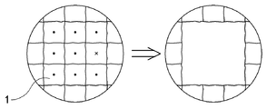
본 발명의 실시예에 따르면 상기 제1이미지획득부(810)에 의하여 획득된 이미지는 웨이퍼링(10)을 기준으로 각 소자(1)의 위치, 즉 제1이송툴(500)의 픽커(513)들에 의하여 픽업될 소자(1)의 위치를 파악하는데 사용될 수 있다.The image obtained by the first
그리고 상기 제1이미지획득부(810)에 의하여 획득된 이미지를 토대로 웨이퍼링(10) 중 소자(1)가 부착되지 않은 위치(도 6에서 ×로 표시)의 파악도 가능하여 소자 부존재에 따른 제1이송툴(500)의 오작동을 방지하여 제1이송툴(500)에 의한 소자 픽업 효율을 높일 수 있다.It is also possible to grasp the position (indicated by x in Fig. 6) of the
또한 웨이퍼 상태에서 소잉을 마친 후 각 소자(1)는 실제로는 도 2에 도시된 바와 같이 절단되지 않고 가로 또는 세로방향으로 편차를 가지고 절단된다.In addition, after the sowing in the wafer state, each
그런데 상기 제1이미지획득부(810)에 의하여 획득된 이미지는 복수의 소자(1)들을 포함하므로 인접한 소자(1)의 배치에 있어서 가로 또는 세로방향으로 편차의 인식도 가능하여 제1이송툴(500)에 의한 소자 픽업 효율을 높일 수 있다.Since the image obtained by the first
도 1은, 본 발명에 따른 소자핸들러의 개념을 보여주는 평면도이다.
도 2a 및 도 2b는 도 1의 소자핸들러에서 사용되는 웨이퍼링을 보여주는 사시도 및 단면도이다.
도 3은, 도 1에서 Ⅲ-Ⅲ방향의 단면도이다.
도 4는 도 1의 소자핸들러에서 사용되는 적재부재의 변형례를 보여주는 평면도이다.
도 5는, 도 1의 소자핸들러의 개념을 보여주는 측면도이다.
도 6은, 도 1의 소자핸들러 중 제1이미지획득부에 의하여 획득된 이미지 및 제1이송툴에 의한 소자픽업 후의 모습을 보여주는 개념도이다.
도 7a 내지 도 7c는, 도 1의 소자핸들러 중 제1이송툴의 저면을 보여주는 저면도들이다.
도 8은, 도 1의 소자핸들러 중 제1이송툴의 변형례를 보여주는 평면도이다.
도 9a 및 도 9b는 본 발명에 따른 소자핸들링방법을 도시하는 일부 개념도들로서, 도 9a는 제1이미지획득부에 의하여 이미지를 획득하는 제1이미지획득단계를 수행하는 개념도이며, 도 9b는 소자이송단계를 보여주는 개념도이다.
도 10a 및 도 10b는 도 9a 및 도 9b에 도시된 소자핸들링방법을 도시하는 일부 평면도로서, 도 10a는 제1이미지획득부에 의하여 이미지를 획득하는 제1이미지획득단계를 수행하는 일부 평면도이며, 도 10b는 소자이송단계를 보여주는 일부 평면도이다.
도 11은 도 1의 소자핸들러의 변형예를 보여주는 측면도이다.1 is a plan view showing the concept of a device handler according to the present invention.
2A and 2B are a perspective view and a cross-sectional view showing a wafer ring used in the device handler of FIG.
Fig. 3 is a sectional view in the III-III direction in Fig. 1. Fig.
4 is a plan view showing a modification of the loading member used in the element handler of FIG.
Fig. 5 is a side view showing the concept of the element handler of Fig. 1; Fig.
FIG. 6 is a conceptual diagram showing an image obtained by the first image acquiring unit and a post-element pickup by the first transfer tool, out of the element handlers of FIG. 1;
Figs. 7A to 7C are bottom views showing the bottom surface of the first transfer tool of the element handler of Fig. 1; Fig.
Fig. 8 is a plan view showing a modification of the first transfer tool of the element handler of Fig. 1; Fig.
9A and 9B are conceptual diagrams showing partly illustrating a device handling method according to the present invention. FIG. 9A is a conceptual view of performing a first image acquiring step of acquiring an image by a first image acquiring unit, FIG. Fig.
10A and 10B are partial plan views showing the element handling method shown in FIGS. 9A and 9B, FIG. 10A is a partial plan view of performing a first image acquiring step of acquiring an image by the first image acquiring unit, 10B is a partial plan view showing the element transferring step.
Fig. 11 is a side view showing a modification of the element handler of Fig. 1; Fig.
이하 본 발명에 따른 소자핸들러에 관하여 첨부된 도면을 참조하여 상세히 설명하면 다음과 같다.Hereinafter, a device handler according to the present invention will be described in detail with reference to the accompanying drawings.
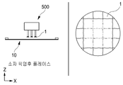
본 발명에 따른 소자핸들러는, 도 1에 도시된 바와 같이, 반도체공정 및 소잉공정을 마친 다수의 소자(1)들이 부착된 웨이퍼링(10)의 적어도 일부에 대한 이미지로서 복수의 소자(1)들을 포함하는 이미지를 획득하는 제1이미지획득부(810)와; 제1이미지획득부(810)에 의하여 획득된 이미지로부터 계산된 각 소자위치에 따라서 제1이미지획득부(810)에 의하여 획득된 이미지에 포함된 복수의 소자(1)들을 모두 픽업한 후 선형이동 및 회전이동 중 적어도 어느 하나의 이동에 의하여 적재부재(20)로 소자(1)를 전달하는 하나 이상의 제1이송툴(500)을 포함한다.A device handler according to the present invention comprises a plurality of
그리고 본 발명에 따른 소자핸들러는, 웨이퍼 상태에서 반도체공정 및 소잉공정을 마친 다수의 소자(1)들이 부착된 복수의 웨이퍼링(10)들이 적재된 웨이퍼링카세트부(100)와; 웨이퍼링카세트부(100)로부터 웨이퍼링(10)을 공급받아 웨이퍼링(10)을 수평방향으로 이동하는 웨이퍼링테이블(200)과; 웨이퍼링테이블(200)로부터 수평방향으로 이격되어 설치되며 웨이퍼링(10)으로부터 소자(1)를 전달받아 적재하는 적재부재(20)가 설치된 언로딩부(300)를 포함할 수 있다.The device handler according to the present invention comprises: a wafer
상기 웨이퍼링카세트부(100)는, 웨이퍼 상태에서 반도체공정 및 소잉공정을 마친 다수의 소자(1)들이 부착된 복수의 웨이퍼링(10)들이 적재된 구성으로서 다양한 구성이 가능하다.The wafer
여기서 상기 웨이퍼링(10)에 적재되는 소자는, 웨이퍼상태에서 반도체공정 및 소잉공정을 마친 소자이다.Here, the device mounted on the
특히 상기 소자(1)는, 반도체공정 후 패키징공정을 거치는 기존 소자와는 달리, 패키징공정을 요하지 않은 소위, 웨이퍼레벨소자가 그 대상이 될 수 있다.Particularly, the
한편 상기 웨이퍼링(10)은, 도 2a 및 도 2b에 도시된 바와 같이, 반도체공정 및 소잉공정을 마친 소자(1)가 적재되는 구성으로서, 소자(1)가 부착되는 테이프(11) 및 테이프(11)를 고정하는 프레임부재(12)를 포함하여 구성될 수 있다.2A and 2B, the
그리고 상기 테이프(11)는 소자(1)들이 부착될 수 있는 부재이면 어떠한 부재도 가능하며 소위 블루테이프가 사용될 수 있다.The
상기 프레임부재(12)는 소자(1)들이 부착된 테이프(11)를 고정하기 위한 구성으로서 원형링, 사각링 등 다양한 구성이 가능하다.The
한편 상기 적재부재(20)는, 소자가 적재되는 구성이면 어떠한 구성도 가능하며, 도 1에 도시된 바와 같은 테이프앤릴(캐리어테이프 및 커버테이프), 블루테이프를 구비한 플레이트, 소자(1)가 담기는 복수의 삽입홈들이 형성된 트레이 등 시장출하 또는 타공정 수행을 위하여 임시로 적재되는 다양한 부재가 사용될 수 있다.On the other hand, the loading
또한 상기 적재부재(20)는, 소자(1)가 임시로 적재되는 부재 이외에, 소자(1)가 실장되는 PCB와 같은 기판, 스트립(strip), 칩제조를 위한 리드프레임(Lead Frame) 등 칩실장, 패키징 공정을 위한 부재가 사용될 수 있다.The stacking
상기 웨이퍼링카세트부(100)는, 복수의 웨이퍼링(10)의 적재를 위한 구성으로서 웨이퍼링(10)들이 상하로 적층될 수 있는 구성이면 어떠한 구성도 가능하다.The wafer
상기 웨이퍼링테이블(200)은, 웨이퍼링카세트부(100)로부터 웨이퍼링(10)을 공급받아 웨이퍼링(10)을 수평방향으로 이동시키는 구성으로서 다양한 구성이 가능하다.The wafer ring table 200 can be variously configured as a structure for moving the
예로서, 상기 웨이퍼링테이블(200)은 웨이퍼링로딩부(미도시)에 의하여 웨이퍼링카세트부(100)로부터 웨이퍼링(10)을 전달받아 제1이송툴(400)이 소자(1)를 픽업할 수 있도록 웨이퍼링(10)을 수평방향으로 이동시키는 구성으로서, X-Y테이블, X-Y-θ테이블 등 다양한 구성이 가능하다.For example, the wafer ring table 200 receives the
또한 상기 웨이퍼링테이블(200)은 상하방향 즉, Z축방향으로 이동될 수도 있다.Further, the wafer ring table 200 may be moved in the vertical direction, i.e., the Z-axis direction.
한편 상기 웨이퍼링카세트부(100)로부터 웨이퍼링테이블(200)로 웨이퍼링(10)을 전달하기 위한 웨이퍼링로딩부는, 웨이퍼링카세트부(100)로부터 웨이퍼링(10)을 인출하고 인출된 웨이퍼링(10)을 웨이퍼링테이블(200)로 전달할 수 있는 구성이면 어떠한 구성도 가능하다.The wafer ring loading section for transferring the
상기 언로딩부(300)는, 웨이퍼링테이블(200)로부터 수평방향으로 이격되어 설치되며 웨이퍼링(10)으로부터 소자(1)를 전달받아 적재하는 적재부재(20)가 설치된 구성으로서 다양한 구성이 가능하다The
특히 상기 언로딩부(300)는, 테이프앤릴(캐리어테이프 및 커버테이프) 등 적재부재(20)의 구성에 따라서 그 구성이 결정된다.Particularly, the configuration of the
예로서, 상기 언로딩부(300)는, 도 1, 도 3, 도 5 및 도 11에 도시된 바와 같이, 소자(1)가 적재되는 포켓부(21)가 길이방향을 따라서 형성되며 소자적재 후 테이프(미도시)에 의하여 밀봉되는 캐리어테이프가 적재부재(20)를 구성하는 경우 일단에 회전가능하게 설치되어 소자(1)가 적재될 캐리어테이프가 감겨진 풀림롤부(311)와, 타단에 회전가능하게 설치되며 소자적재 후 테이프에 의하여 밀봉된 캐리어테이프가 감기는 감길롤부(312)와, 풀림롤부(311)로부터 풀린 캐리어테이프가 적재위치를 지나도록 캐리어테이프의 이동을 안내하는 캐리어테이프가이드부(313)를 포함하여 구성될 수 있다.1, 3, 5, and 11, the
여기서 상기 적재부재(20)는 도 3에 도시된 바와 같이, 소자(1)가 담겨지는 포켓부(21)의 저면에 복수의 홀(22)들이 형성될 수 있다.3, a plurality of
그리고 상기 적재부재(20)가 적재위치에 위치되었을 때 적재부재(20)의 직하방에 진공압을 형성하는 진공압형성장치(24)가 설치되어 후술하는 제1이송툴(500)에 의하여 적재될 때 소자(1)가 안정적으로 적재될 수 있도록 할 수 있다.And a vacuum
여기서 상기 적재부재(20)가 캐리어테이프인 경우 도 3에 도시된 바와 같이, 캐리어테이프의 날개부분을 가이드하도록 설치된 한 쌍의 롤러부재(28)와, 롤러부재가 고정되는 지지부재(29)의 가이드에 의하여 그 이동이 가이드될 수 있다.As shown in FIG. 3, when the
상기 언로딩부(300)의 다른 예로서, 적재부재(20)가 부착되는 플레이트(도 4 참조)인 경우로서, 언로딩부(300)는, 일단에 위치되어 복수의 소자(1)들이 부착되는 플레이트가 적재되는 플레이트적재부와, 제1이송툴(500)에 의하여 소자(1)들을 전달받도록 적재위치에서 플레이트를 지지하여 이동시키는 X-Y테이블과, 트레이적재부로부터 플레이트를 X-Y테이블로 전달하는 트레이이동부(미도시)를 포함하여 구성될 수 있다. As another example of the unloading
여기서 상기 플레이트는, 도 4에 도시된 바와 같이, 웨이퍼링(10)과 유사한 구성으로서 소자(1)가 부착되는 테이프(21)와, 테이프(21)를 고정시키면서 LOT번호, 분류등급 등의 표식이 있는 지지부재(14)를 포함하여 구성되거나, 소자(1)가 담기는 삽입홈들이 복수개로 형성된 트레이로서, 소자(1)의 종류에 따라서 규격화된 트레이, 즉, JEDEC 트레이가 사용될 수 있다.4, the plate is provided with a
또한 도 4에 도시된 플레이트는, 도 1에서 리젝부(700)의 트레이(30), 언로딩부(300)의 구성에 따라서 언로딩부(300)에서 사용될 수 있다.The plate shown in FIG. 4 can be used in the unloading
한편 상기 언로딩부(300)는, 도 1에 도시된 바와 같이, 캐리어테이프에 소자(1)를 적재하는 구성1(310), 플레이트에 소자(1)를 적재하는 구성2 등 어느 하나로만 구성되거나, 구성 1 및 2 중 2개, 또는 모두를 포함하여 구성될 수 있다.1, the
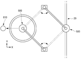
상기 제1이미지획득부(810)는 웨이퍼링테이블(200)의 상측에 설치되며 웨이퍼링테이블(200)에 안착된 웨이퍼링(10)에 부착된 소자(1)들의 일부에 대한 이미지를 획득하는 구성으로서 CCD카메라 등으로 구성될 수 있다.The first
또한 상기 제1이미지획득부(810)는, 도 6에 도시된 바와 같이, 웨이퍼링(10)에 부착된 소자(1)들의 일부에 대한 이미지를 획득하고 획득된 이미지를 제어부(미도시)에 전달할 수 있다.6, the first
그리고 상기 제1이미지획득부(810)에 의하여 획득된 이미지는 웨이퍼링(10)을 기준으로 각 소자(1)의 위치, 즉 후술한 제1이송툴(500)의 픽커(513)들에 의하여 픽업될 각 소자(1)의 소자위치를 파악하는데 사용될 수 있다.The images obtained by the first
또한 상기 제1이미지획득부(810)에 의하여 획득된 이미지를 토대로 웨이퍼링(10) 중 소자(1)가 부착되지 않은 위치(도 6에서 ×로 표시)의 파악도 가능하여 후술하는 제1이송툴(500)에 의한 소자 픽업 효율을 높일 수 있다.Also, it is possible to grasp the position (indicated by x in Fig. 6) of the
또한 웨이퍼 상태에서 소잉을 마친 후 각 소자(1)는 실제로는 도 2에 도시된 바와 같이 절단되지 않고 가로 또는 세로방향으로 편차를 가지고 절단된다.In addition, after the sowing in the wafer state, each
그런데 상기 제1이미지획득부(810)에 의하여 획득된 이미지는 복수의 소자(1)들을 포함하므로 인접한 소자(1)의 배치에 있어서 가로 또는 세로방향으로 편차의 인식도 가능하여 후술하는 제1이송툴(500)에 의한 소자 픽업 효율을 높일 수 있다.Since the image obtained by the first
그러나 종래의 소자핸들러의 경우 카메라에 의하여 각 소자에 대한 인식 후 소자를 픽업하는데 픽업될 위치에서 소자(1)가 없거나 편차가 있음에도 불구하고 해당 위치의 인식 후에야 비로소 소자(1)가 없거나 편차가 있음을 인식하게 되어 소자 픽업 효율이 저하된다.However, in the case of the conventional device handler, the device picks up the device after recognizing each device by the camera, and there is no or variation in the device (1) only after recognizing the position, The element pickup efficiency is lowered.
이에 반하여 본 발명의 경우 소자(1)가 부착되지 않은 위치(도 6에서 ×로 표시), 인접한 소자(1)의 배치의 편차의 인식이 사전에 가능하여 후술하는 제1이송툴(500)에 의한 소자 픽업 효율을 높일 수 있다.On the contrary, in the present invention, it is possible to recognize the deviation of the arrangement of the adjacent elements 1 (indicated by x in Fig. 6) where the
또한 상기 제1이미지획득부(810)에 의하여 획득된 이미지는 웨이퍼링(10)에 부착된 소자(1)의 상면에 대한 비전검사에 사용될 수 있다.The image acquired by the first
한편 상기 제1이미지획득부(810)에 의하여 획득된 복수의 소자(1)들에 대한 이미지는 제어부(미도시)에 전달된 후 분석되며, 제어부는 소자(1)의 유무, 소자(1)의 위치, 소자(1)의 상태 등을 분석하게 된다.Meanwhile, the image of the plurality of
특히 상기 제어부는, 제1이미지획득부(810)에 의하여 획득된 복수의 소자(1)들에 대한 이미지를 분석하고 그 분석결과에 따라서 미리 설정된 판단기준에 따라서 적합한 것으로 판단된 경우 언로딩부(300)의 적재부재(20)로, 부적합한 것으로 판단된 경우 별도로 설치된 소자수거부로 제거되거나, 앞서 설명한 리젝부(700)로 소자(1)가 전달되도록 한다.Particularly, the controller analyzes the images of the plurality of
상기 제어부는, 웨이퍼링(10)에 부착된 소자(1)들의 일부에 대한 이미지를 전달받아 후술하는 제1이송툴(500)에 의하여 소자(1)의 픽업이 가능하도록 웨이퍼링(10) 상에서의 각 소자(1)의 소자위치를 계산하는 구성으로서 제1이미지획득부(810)와 함께 구성되거나 별도로 구성되는 등 다양한 구성이 가능하다.The control unit receives an image of a part of the
또한 상기 제어부는, 웨이퍼링(10)에 부착된 소자(1)들의 일부에 대한 이미지를 전달받아 소자위치의 계산과 함께 소자(1)에 대한 비전검사를 함께 수행할 수도 있다.The control unit may also receive an image of a part of the
한편 상기 제1이미지획득부(810)는 소자(1)에 대한 정밀한 인식을 요하는바 웨이퍼링(10)에 가깝게 배치될 필요가 있다.Meanwhile, the first
그러나 상기 제1이미지획득부(810)이 웨이퍼링(10)에 가깝게 설치되는 경우 제1이송툴(810)과의 간섭이 발생된다.However, when the first
따라서, 본 발명에 따른 소자핸들러는, 도 9a 내지 도 10b에 도시된 바와 같이, 제1이미지획득부(810)를 이미지가 획득될 웨이퍼링(10) 상의 제1위치와, 제1이송툴(500)에 의한 소자픽업시 간섭되지 않는 제2위치로 이동시키는 제1이동부(미도시)를 포함할 수 있다.9A to 10B, the device handler according to the present invention can be configured such that the first
상기 제1이동부는, 제1이미지획득부(810)를 이미지가 획득될 웨이퍼링(10) 상의 제1위치와, 제1이송툴(500)에 의한 소자픽업시 간섭되지 않는 제2위치로 이동시킬 수 있는 구성이면 어떠한 구성도 가능하다.The first moving unit moves the first
상기 제1이동부는, 제1이미지획득부(810)를 수평방향의 선형이동, 회전이동 등에 의하여 제1이미지획득부(810)를 이동하도록 구성될 수 있다.The first moving unit may be configured to move the first
또한 상기 제1이동부는, 제1이미지획득부(810)를 제1이송툴(500)에 의하여 소자픽업시 상측으로 이동될 수 있다.Further, the first moving unit may be moved upward when the first
상기 제1이송툴(500)은 제1이미지획득부(810)에 의하여 획득된 이미지 내에 포함된 복수의 소자(1)들을 획득된 이미지를 이용하여 픽업위치로 이동하여 획득된 이미지 내에 포함된 복수의 소자(1)들을 모두 픽업한 후 선형이동 및 회전이동 중 적어도 어느 하나의 이동에 의하여 언로딩부(300)의 적재부재(20)로 소자(1)를 전달하는 구성이다.The
일예로서, 상기 제1이송툴(500)은, 도 1, 도 5, 도 7a 내지 도 7c 및 도 8에 도시된 바와 같이, 제1이미지획득부(810)에 의하여 획득된 이미지 내에 포함된 복수의 소자(1)들을 획득된 이미지를 이용하여 픽업위치로 이동하여 획득된 이미지 내에 포함된 복수의 소자(1)들을 모두 픽업할 수 있도록, 복수의 픽커(513)들을 포함할 수 있다.As an example, the
그리고 상기 이송툴(500)의 픽커(513)들의 지지구조 및 구동방식에 따라서 다양한 구성이 가능하다.Various configurations are possible according to the supporting structure of the
상기 제1이송툴(500)은, 도 1, 도 5, 도 7a 내지 도 7c에 도시된 바와 같이, 복수의 픽커(513)들과, 복수의 픽커(513)들이 지지되어 설치되는 지지부재(514)를 포함할 수 있다.The
상기 복수의 픽커(513)들은, 진공압에 의하여 웨이퍼링(10)으로부터 소자(1)를 픽업하는 구성으로서 다양한 구성이 가능하다.The plurality of
상기 복수의 픽커(513)들은, 웨이퍼링(10) 상에 부착된 소자(1)들이 거의 직각으로 배치된 행렬배치를 이룸이 일반적인바 제1이송툴(810)은, 이에 대응되어 n×m배열(n은 1 이상의 자연수, m은 2 이상의 자연수)로 배치될 수 있다.The plurality of
상기 복수의 픽커(513)들의 소자픽업에 있어서 웨이퍼링(10) 상에 부착된 소자(1)들을 한번에 픽업할 수 있으나 위치편차 등을 고려하여, 웨이퍼링(10)과의 상대이동에 의하여 하나씩 소자(1)를 픽업할 수 있다.The
한편 상기 지지부재(514)는, 도 7a 내지 도 7c에 도시된 바와 같이, 복수의 픽커(513)들이 지지되는 방향에서, 즉 저면의 형상이 원형, 타원형, 다각형 등 다양한 형상을 가질 수 있다.7A to 7C, the
상기 제1이송툴(500)의 다른 예로서, 제1이송툴(500)은, 도 8에 도시된 바와 같이, 회전구동하는 회전모터(515)의 회전축을 중심으로 각각 방사상으로 배치되는 복수의 픽커(513)들을 포함할 수 있다.As another example of the
이때 상기 제1이송툴(500)을 기준으로 웨이퍼링(10) 및 적재부재(20)는 서로 대향되는 위치, 즉 X축방향으로 배치됨이 바람직하다.At this time, it is preferable that the
한편 상기 제1이송툴(500)은, 제1이미지획득부(810)에 의한 이미지 획득 및 분석 후에 획득된 이미지 내에 포함, 즉 이미지 분석이 가능한 모든 해당 소자(1)들을 픽업한다.On the other hand, the
즉, 본 발명에 따른 소자핸들러는, 제1이미지획득부(810)에 의한 이미지 획득 및 분석 후에 획득된 이미지 내에 포함, 즉 이미지 분석이 가능한 모든 해당 소자(1)들을 픽업하여 이송함으로써 소자언로딩 속도를 현저히 높일 수 있다.That is, the device handler according to the present invention picks up and transfers all the
한편 상기 제1이송툴(500)는, 하나의 선형이동, 즉 X축방향 또는 Y축방향의 선형이동, 소자(1)를 2개 이상의 선형이동, 즉 X축방향, Y축방향 및 Z축방향의 선형이동들 중 2개 또는 3개의 이동들에 의하여 소자(1)를 픽업하고 있는 복수의 픽커(513)들을 이동시키는 피커이동부를 포함할 수 있다.Meanwhile, the
이 경우 상기 픽커이동부는, 선형이동의 수에 따른 선형이동부(미도시)들을 포함할 수 있다.In this case, the picker moving unit may include linear moving units (not shown) according to the number of linear movements.
예를 들면 상기 제1이송툴(500)은, 도 1에 도시된 바와 같이, 웨이퍼링(10)과 적재부재(20) 사이로 가이드레일(522, 532)을 따라서, 즉 X축방향으로 선형이동되도록 설치될 수 있다. For example, the
이때 상기 복수의 픽커(513)들을 지지하는 지지부재(514)들은 가이드레일(522, 532)을 따라서 선형이동되는 지지브라켓(521, 531)에 의하여 지지되며 Y축방향으로 선형이동되도록 설치될 수 있다.The
한편 상기 제1이송툴(500)은, 소자(1)의 이송효율을 고려하여 평행하게 한 쌍으로 설치되고, 이때 적재부재(20)는 한 쌍의 제1이송툴(500)이 이루는 평행한 방향과 수직방향으로 이동될 수 있다.Meanwhile, the
또한 상기 제1이송툴(500)이 한 쌍으로 구성된 경우 상하로 이동, 또는 Y축방향으로 이동됨으로써 상호가 이동시 간섭을 방지할 수 있다.In addition, when the
또한 이동방식에 따른 상기 제1이송툴(500)의 실시예로서, 웨이퍼링(10) 및 적재부재(20)의 배치방향을 X축방향, 수평면 상에서 X축과 수직인 방향을 Y축방향, X축 및 상기 Y축과 수직인 방향을 Z축방향, Z축을 회전축으로 하는 회전방향을 θ방향이라고 할 때, 제1이송툴(500)은, X축방향 선형이동, Y축방향 선형이동, Z축방향 선형이동 및 θ방향 회전이동에 의하여 웨이퍼링(10)으로부터 소자(10)를 픽업하도록 구성될 수 있다.As an example of the
이때 상기 웨이퍼링(10)에서 픽업될 소자(1)에 대한 소자위치에 대한 보정은 제1이송툴(500)의 X축방향 선형이동, Y축방향 선형이동, Z축방향 선형이동 및 θ방향 회전이동에 의하여 수행될 수 있다.At this time, the correction of the element position with respect to the
여기서 상기 웨이퍼링(10)에서 픽업될 소자(1)에 대한 소자위치에 대한 보정은 웨이퍼링(10)이 적재된 웨이퍼링테이블(200)에 의해서도 수행될 수 있음은 물론이다.It should be understood that the correction of the element position with respect to the
또한 이동방식에 따른 상기 제1이송툴(500)의 실시예로서, 제1이송툴(500)은, 웨이퍼링테이블(200)의 이동과 함께 X축방향 선형이동 및 Y축방향 선형이동에 의하여 웨이퍼링(10)으로부터 소자(1)를 픽업하도록 구성될 수 있다.In addition, as an example of the
여기서 웨이퍼링(10)은 제1이송툴(500)에 의하여 소자(1)가 픽업될 때 웨이퍼링테이블(200)에 위하여 Z축방향 선형이동 및 θ방향 회전이동되며, 상기 웨이퍼링(10)에서 픽업될 소자(1)에 대한 소자위치에 대한 보정은 웨이퍼링(10)이 적재된 웨이퍼링테이블(200), 웨이퍼링테이블(200)의 Z축방향 선형이동 및 θ방향 회전이동에 의해서도 수행될 수 있다.Here, the
한편 적재부재(20)에 적재되는 소자(1)는 공정조건, 소자의 종류 등에 따라서 웨이퍼링(10)에서의 상면이 저면으로 되어 적재, 즉 반전되어 적재될 필요가 있는 경우가 있다.On the other hand, the
이에 본 발명에 따른 소자핸들러는, 도 1 내지 도 8에 도시된 바와 같은 실시예와 달리, 도 11에 도시된 보와 같이, 제1이송툴(810)은 제1이미지획득부(810)에 의하여 획득된 이미지 내에 포함된 복수의 소자(1)들을 모두 픽업한 후 저면이 상측을 항하도록 180°회전하여 픽업된 소자(1)들을 반전시키며, 제1이송툴(810)에 의하여 반전된 소자(1)를 픽업한 후 선형이동 및 회전이동 중 적어도 어느 하나의 이동에 의하여 언로딩부(300)의 적재부재(20)로 소자(1)를 전달하는 제2이송툴(600)을 추가로 포함할 수 있다.The device handler according to the present invention differs from the first embodiment shown in FIGS. 1 to 8 in that the
상기 제1이송툴(810)은 상하로 180°회전하는 것 이외에는 구성이 실질적으로 동일하거나 유사하다.The
이때 제1이송툴(810)은 도 7a 내지 도 7c에 도시된 바와 같은 구성에서 복수의 픽커(513)들이 결합된 지지부재(514)를 180°회전하는 회전장치를 추가로 구비하게 된다.At this time, the first conveying
상기 제2이송툴(600)은, 제1이송툴(810)에 의하여 반전된 소자(1)를 픽업한 후 선형이동 및 회전이동 중 적어도 어느 하나의 이동에 의하여 언로딩부(300)의 적재부재(20)로 소자(1)를 전달하는 구성이다.The second conveying
상기 제2이송툴(600)은, 제1이송툴(810)에 의하여 반전된 소자(1)를 픽업함을 고려하여 제1이송툴(810)과 동일한 배치를 가지도록 구성됨이 바람직하다.The
한편 상기 제2이송툴(600)은, 제1이송툴(400)이 한 쌍으로 배치되는 경우 이에 대응되어 평행하게 한 쌍으로 설치될 수 있다.On the other hand, when the first transfer tools 400 are arranged in pairs, the
이 경우 앞서 설명한 언로딩부(300)에서 적재부재(20)는 한 쌍의 제2이송툴(600)이 이루는 평행한 방향과 수직방향으로 이동될 수 있다.In this case, the loading
상기와 같이 제2이송툴(600)이 한 쌍으로 구성됨으로써 신속하게 소자(1)의 이송이 가능하다.As described above, the
그리고 상기 제2이송툴(600)이 한 쌍으로 구성된 경우 상하로 이동, 또는 Y축방향으로 이동됨으로써 상호가 이동시 간섭을 방지할 수 있다.When the second conveying
한편 본 발명에 따른 소자핸들러는 웨이퍼링(10)에 적재된 소자(1)는 별도의 검사장치에 의하여 미리 검사된 상태이며 미리 검사된 검사결과에 따라서 부적합한 것으로 판단된 양품의 소자(1)만 적재부재(20)에 적재하도록 구성될 수 있다.In the device handler according to the present invention, the
이때 상기 소자핸들러는, 미리 검사된 검사결과에 따라서 부적합한 것으로 판단된 소자(1)가 제2이송툴(600)에 의하여 적재되는 리젝적재부재(30)가 설치된 리젝부(700)를 추가로 포함할 수 있다.At this time, the device handler further includes a
상기 리젝부(700)는, 언로딩부(300)의 구성의 예 중 트레이를 구비한 구성과 유사한 구성을 가질 수 있다. 아울러, 소자이송의 효율화를 위하여 도 1에 도시된 바와 같이, 제1이송툴(400)을 중심으로 언로딩부(300)에 대향되어 설치됨이 바람직하다.The
한편 상기 소자핸들러는, 제1이송툴(500) 또는 제2이송툴(600)에 의하여 소자(1)가 이송될 때 검사되지 않은 소자(1)의 저면에 이미지를 획득하는 제2이미지획득부(820)를 추가로 포함할 수 있다.On the other hand, the element handler is provided with a second
상기 제2이미지획득부(820)는, 제1이송툴(500) 또는 제2이송툴(600)에 의한 소자(1)의 픽업상태에서 소자(1)의 저면에 대한 이미지를 획득하는 구성으로서 CC카메라 등이 사용될 수 있다.The second
한편 상기 제2이미지획득부(820)에 의하여 획득된 이미지는 제어부에 전달되고 제어부에 의한 이미지분석에 의하여 제1이송툴(500) 또는 제2이송툴(600)의 회전이동 및 선형이동과, 적재부재(20)의 선형이동의 조합 등 다양한 조합에 의하여 제1이송툴(500) 또는 제2이송툴(600)에 의하여 픽업된 소자(1)의 소자(1)의 적재위치의 정렬을 수행할 수 있다. Meanwhile, the image obtained by the second
또한 상기 소자핸들러는, 제1이송툴(500) 또는 제2이송툴(600)이 적재위치에서 소자(1)를 적재부재(20)에 적재한 후 그 적재상태에 대한 이미지를 획득하는 제3이미지획득부(미도시)를 추가로 포함할 수 있다.The device handler may also be configured such that after the
상기 제3이미지획득부는, 소자(1)가 적재부재(20)에 적재된 후 그 적재상태에 대한 이미지를 획득하여 분석함으로써 적재부재(20)에 부적절하게 적재된 것으로 판단된 경우 시스템을 정지시키거나, 음향 또는 시각신호를 통하여 불적절하게 적재되었음을 알리거나, 제1이송툴(500) 또는 제2이송툴(600)에 의하여 소자(1)를 재 픽업하여 버리거나 재적재하는 등 적절한 조치를 취할 수 있도록 할 수 있다.The third image acquiring unit stops the system when it is judged that the
또한 상기 소자핸들러는, 캐리어테이프가 커버테이프(미도시)에 의하여 밀봉된 후 커버테이프가 부착된 캐리어테이프에 대한 이미지를 획득하는 제4이미지획득부(미도시)를 추가로 포함할 수 있다.The device handler may further include a fourth image acquiring unit (not shown) for acquiring an image of the carrier tape to which the cover tape is attached after the carrier tape is sealed by the cover tape (not shown).
상기 제4이미지획득부는, 캐리어테이프가 커버테이프(미도시)에 의하여 밀봉된 후 커버테이프가 부착된 캐리어테이프에 대한 이미지를 획득하여 분석함으로써 그 밀봉상태가 부적절한 것으로 판단된 경우 시스템을 정지시키거나, 음향 또는 시각신호를 통하여 불적절하게 밀봉되었음을 알리거나, 캐리어테이프를 반대로 이동시켜 실링을 재수행하는 등 적절한 조치를 취할 수 있도록 할 수 있다.The fourth image acquiring unit acquires and analyzes an image of the carrier tape on which the cover tape is attached after the carrier tape is sealed by the cover tape (not shown), thereby stopping the system when it is determined that the sealed state is inappropriate , It is possible to notify that it is improperly sealed through an acoustic or visual signal, or to take appropriate measures such as moving the carrier tape in reverse to re-execute the sealing.
한편 상기와 같은 구성을 가지는 소자핸들러는, 반도체공정 및 소잉공정을 마친 다수의 소자(1)들이 부착된 웨이퍼링(20)의 적어도 일부에 대한 이미지로서 복수의 소자(1)들을 포함하는 이미지를 획득하는 제1이미지획득단계와; 제1이미지획득단계에 의하여 획득된 이미지에 포함된 복수의 소자(1)들을 획득된 이미지를 이용하여 제1이미지획득단계에서 획득된 이미지에 포함된 복수의 소자(1)들의 각 소자위치를 계산하는 위치계산단계와; 소자(1)들을 픽업하기 위한 제1이송툴(500)을 위치계산단계에서 계산된 소자(1)들의 각 소자위치들로 순차적으로 이동시켜 제1이미지획득단계에서 획득된 이미지에 포함된 복수의 소자(1)들을 모두 픽업한 후 선형이동 및 회전이동 중 적어도 어느 하나의 이동에 의하여 적재부재(20)로 소자를 전달하는 소자이송단계를 포함하는 것을 특징으로 하는 소자핸들링방법을 구현할 수 있다On the other hand, the element handler having the above-described configuration is an element handler in which an image including a plurality of
상기 제1이미지획득단계는, 반도체공정 및 소잉공정을 마친 다수의 소자(1)들이 부착된 웨이퍼링(20)의 적어도 일부에 대한 이미지로서 복수의 소자(1)들을 포함하는 이미지를 획득하는 단계로서 다양한 방법에 의하여 수형될 수 있다.The step of acquiring an image comprises acquiring an image comprising a plurality of elements (1) as an image for at least a part of a wafer ring (20) with a plurality of devices (1) Can be embodied by various methods.
한편 상기 제1이미지획득단계는, 도 9a 및 도 10a에 도시된 바와 같이, 웨이퍼링(10) 상부에 위치되어 웨이퍼링(10)의 적어도 일부에 대한 이미지를 획득하는 제1이미지획득부(810)에 의하여 수행되며, 소자이송단계는, 도 9b 및 도 10b에 도시된 바와 같이, 제1이미지획득부(810)를 이미지가 획득될 웨이퍼링(10) 상의 제1위치와, 제1이송툴(500)에 의한 소자픽업시 간섭되지 않는 제2위치로 이동시킬 수 있다.The first image acquisition step, on the other hand, includes a first image acquisition unit 810 (see FIG. 9A) that acquires an image for at least a portion of the
도 10a 및 도 10b에 도시된 실시예의 경우, 선형이동만이 가능한 도 1에 도시된 제1이송툴(500)과는 달리 웨이퍼링(10) 상의 소자픽업위치에서 적재부재(20) 상의 소자적재위치로 수평회전에 의하여 이동되는 예를 도시한 것이다.10A and 10B, in contrast to the
한편 본 발명에 따른 소자핸들링방법은, 제1이미지획득단계에서 획득된 이미지에 포함된 복수의 소자(1)들에 대한 비전검사가 수행하는 비전검사단계를 추가로 포함할 수 있다.Meanwhile, the device handling method according to the present invention may further include a vision inspection step performed by the vision inspection of the plurality of
상기 소자이송단계는, 비전검사단계에서 불량으로 검사된 소자(1)를 제외하고 픽업하거나, 픽업 후 적재부재(20) 상에 위치되기 전에 제1이송툴(500)에서 제거될 수 있다.The element transferring step may be picked up except for the
상기 위치계산단계는, 웨이퍼링(10)에 대한 이미지에서 각 소자(1)의 소자위치를 계산하며, 소자이송단계는, 소자(1)가 있는 것으로 계산된 소자위치들에 대해서만 제1이송툴(500)을 이동시켜 소자(1)를 픽업할 수 있다.
The position calculating step calculates the element position of each element (1) in the image for the wafer ring (10), and the element transfer step is performed only for the element positions calculated as having the element (1) The
이상은 본 발명에 의해 구현될 수 있는 바람직한 실시예의 일부에 관하여 설명한 것에 불과하므로, 주지된 바와 같이 본 발명의 범위는 위의 실시예에 한정되어 해석되어서는 안 될 것이며, 위에서 설명된 본 발명의 기술적 사상과 그 근본을 함께 하는 기술적 사상은 모두 본 발명의 범위에 포함된다고 할 것이다.It will be apparent to those skilled in the art that various modifications and variations can be made in the present invention without departing from the spirit or scope of the invention as defined in the appended claims. It is to be understood that both the technical idea and the technical spirit of the invention are included in the scope of the present invention.
100 : 웨이퍼링카세트부
200 : 웨이퍼링테이블
300 : 언로딩부
500 : 제1이송툴
810 : 제1이미지획득부100: wafer ring cassette 200: wafer ring table
300: unloading unit 500: first transfer tool
810: First image acquiring unit
Claims (18)
상기 제1이미지획득부에 의하여 획득된 이미지로부터 계산된 각 소자위치에 따라서 상기 제1이미지획득부에 의하여 획득된 이미지에 포함된 복수의 소자들을 모두 픽업한 후 선형이동 및 회전이동 중 적어도 어느 하나의 이동에 의하여 적재부재로 소자를 전달하는 하나 이상의 제1이송툴을 포함하는 것을 특징으로 하는 소자핸들러.A first image acquiring unit for acquiring an image including a plurality of elements as an image of at least a part of a wafer ring to which a plurality of devices having completed semiconductor processing and soaking processes are attached;
At least one of a plurality of elements included in an image obtained by the first image obtaining unit is picked up according to each element position calculated from the image obtained by the first image obtaining unit, Wherein the at least one first transfer tool transfers the element to the loading member by movement of the first transfer tool.
상기 제1이미지획득부를 이미지가 획득될 웨이퍼링 상의 제1위치와, 상기 제1이송툴에 의한 소자픽업시 간섭되지 않는 제2위치로 이동시키는 제1이동부를 포함하는 것을 특징으로 하는 소자핸들러.The method according to claim 1,
And a first moving unit for moving the first image obtaining unit to a first position on the wafer ring where an image is to be obtained and a second position that is not interfered with when the device is picked up by the first transfer tool.
상기 제1이미지획득부에 의하여 획득된 이미지는 상기 제1이미지획득부에 의하여 획득된 이미지에 포함된 복수의 소자들에 대한 비전검사에 사용되는 것을 특징으로 하는 소자핸들러.The method according to claim 1,
Wherein the image obtained by the first image obtaining unit is used for a vision check on a plurality of elements included in the image obtained by the first image obtaining unit.
반도체공정 및 소잉공정을 마친 다수의 소자들이 부착된 복수의 웨이퍼링들이 적재된 웨이퍼링카세트부와;
상기 웨이퍼링카세트부로부터 웨이퍼링을 공급받아 웨이퍼링을 수평방향으로 이동하는 웨이퍼링테이블과;
상기 웨이퍼링테이블로부터 수평방향으로 이격되어 설치되며 상기 제1이송툴에 의하여 상기 웨이퍼링으로부터 소자를 전달받아 적재하는 적재부재가 설치된 언로딩부를 포함하는 것을 특징으로 하는 소자핸들러.The method according to claim 1,
A wafer ring cassette portion on which a plurality of wafer rings with a plurality of devices attached thereto after semiconductor processing and sowing processes are loaded;
A wafer ring table for receiving the wafer ring from the wafer ring cassette and moving the wafer ring horizontally;
And an unloading unit installed in the wafer ring table to be spaced apart in the horizontal direction and provided with a loading member for receiving and transferring the device from the wafer ring by the first transfer tool.
상기 적재부재는, 캐리어테이프, 블루테이프를 구비한 플레이트, 소자가 담기는 복수의 삽입홈들이 형성된 트레이, 소자가 실장되는 기판, 소자가 결합되는 스트립, 및 칩제조를 위한 리드프레임 중 적어도 하나인 것을 특징으로 하는 소자핸들러.The method according to claim 1,
The mounting member may be at least one of a carrier tape, a plate provided with a blue tape, a tray having a plurality of insertion grooves formed therein, a substrate on which the device is mounted, a strip to which the device is coupled, Wherein said device handler comprises:
상기 제1이송툴은 상기 제1이미지획득부에 의하여 획득된 이미지 내에 포함된 복수의 소자들을 모두 픽업한 후 저면이 상측을 항하도록 180°회전하여 픽업된 소자들을 반전시키며,
상기 제1이송툴에 의하여 반전된 소자를 픽업한 후 선형이동 및 회전이동 중 적어도 어느 하나의 이동에 의하여 상기 언로딩부의 적재부재로 소자를 전달하는 제2이송툴을 추가로 포함하는 것을 특징으로 하는 소자핸들러.The method according to claim 1,
Wherein the first transfer tool picks up all of the plurality of elements included in the image acquired by the first image acquiring unit and then rotates 180 ° so that the bottom faces the upper side to invert the picked-
And a second transfer tool for transferring the element to the loading member of the unloading unit by at least one of linear movement and rotational movement after picking up the element inverted by the first transfer tool. Device handler.
상기 제1이송툴은, n×m배열(n은 1 이상의 자연수, m은 2 이상의 자연수)의 복수의 픽커들을 포함하는 것을 특징으로 하는 소자핸들러.The method according to claim 1,
Wherein said first transfer tool comprises a plurality of pickers of an n x m array (n is a natural number of 1 or more, and m is a natural number of 2 or more).
상기 제1이송툴은, 복수의 픽커들과, 상기 복수의 픽커들이 지지되어 설치되는 지지부재를 포함하며,
상기 지지부재는 상기 복수의 픽커들이 지지되는 방향에서 원형, 타원형 및 다각형 중 어느 하나의 형상을 가지는 것을 특징으로 하는 소자핸들러.The method of claim 7,
Wherein the first transporting tool includes a plurality of pickers and a support member on which the plurality of pickers are supported,
Wherein the support member has a shape of a circle, an ellipse, and a polygon in a direction in which the plurality of pickers are supported.
상기 제1이송툴은, 회전구동하는 회전모터의 회전축을 중심으로 각각 방사상으로 배치되는 복수의 픽커들을 포함하는 것을 특징으로 하는 소자핸들러.The method of claim 7,
Wherein the first conveying tool includes a plurality of pickers radially arranged around a rotation axis of a rotary motor driven to rotate.
웨이퍼링 및 상기 적재부재의 배치방향을 X축방향, 수평면 상에서 X축과 수직인 방향을 Y축방향, 상기 X축 및 상기 Y축과 수직인 방향을 Z축방향, 상기 Z축을 회전축으로 하는 회전방향을 θ방향이라고 할 때,
상기 제1이송툴은, X축방향 선형이동, Y축방향 선형이동, Z축방향 선형이동 및 θ방향 회전이동에 의하여 웨이퍼링으로부터 소자를 픽업하는 것을 특징으로 하는 소자핸들러.The method according to claim 1,
A direction in which the wafer ring and the mounting member are arranged in the X axis direction, a direction perpendicular to the X axis on the horizontal plane is a Y axis direction, a direction perpendicular to the X axis and the Y axis is a Z axis direction, When the direction is the &thetas; direction,
Wherein the first transfer tool picks up the element from the wafer ring by linear movement in the X-axis direction, linear movement in the Y-axis direction, linear movement in the Z-axis direction, and rotational movement in the? Direction.
웨이퍼링 및 상기 적재부재의 배치방향을 X축방향, 수평면 상에서 X축과 수직인 방향을 Y축방향, 상기 X축 및 상기 Y축과 수직인 방향을 Z축방향, 상기 Z축을 회전축으로 하는 회전방향을 θ방향이라고 할 때,
상기 웨이퍼링은, 상기 제1이송툴에 의하여 소자가 픽업될 때 웨이퍼링테이블에 위하여 Z축방향 선형이동 및 θ방향 회전이동되며,
상기 제1이송툴은, 상기 웨이퍼링테이블의 이동과 함께 X축방향 선형이동 및 Y축방향 선형이동에 의하여 웨이퍼링으로부터 소자를 픽업하는 것을 특징으로 하는 소자핸들러.The method according to claim 1,
A direction in which the wafer ring and the mounting member are arranged in the X axis direction, a direction perpendicular to the X axis on the horizontal plane is a Y axis direction, a direction perpendicular to the X axis and the Y axis is a Z axis direction, When the direction is the &thetas; direction,
The wafer ring is linearly moved in the Z-axis direction and rotated in the? Direction for the wafer ring table when the element is picked up by the first transfer tool,
Wherein the first transfer tool picks up an element from the wafer ring by linear movement in the X-axis direction and linear movement in the Y-axis direction together with the movement of the wafer ring table.
상기 제1이송툴은, 평행하게 한 쌍으로 설치되고,
상기 적재부재는 상기 한 쌍의 제1이송툴이 이루는 평행한 방향과 수직방향으로 이동되는 것을 특징으로 하는 소자핸들러. The method according to claim 1,
Wherein the first transfer tool is provided in a pair in parallel,
Wherein the stacking member is moved in a direction perpendicular to the parallel direction of the pair of first transfer tools.
소자들이 상기 제1이송툴에 의하여 상기 언로딩부의 적재부재로 전달될 때 상기 제1이송툴에 의하여 픽업된 소자의 저면에 대한 비전검사를 위하여 소자의 저면에 대한 이미지를 획득하는 제2이미지획득부를 추가로 포함하는 것을 특징으로 하는 소자핸들러.The method according to claim 1,
When the elements are transferred to the loading member of the unloading unit by the first transfer tool, acquiring an image of the bottom surface of the element for a vision inspection of the bottom surface of the element picked up by the first transfer tool Wherein the device handler further comprises:
상기 제1이미지획득단계에 의하여 획득된 이미지에 포함된 복수의 소자들을 획득된 이미지를 이용하여 상기 제1이미지획득단계에서 획득된 이미지에 포함된 복수의 소자들의 각 소자위치를 계산하는 위치계산단계와;
소자들을 픽업하기 위한 제1이송툴을 상기 위치계산단계에서 계산된 소자들의 각 소자위치들로 순차적으로 이동시켜 상기 제1이미지획득단계에서 획득된 이미지에 포함된 복수의 소자들을 모두 픽업한 후 선형이동 및 회전이동 중 적어도 어느 하나의 이동에 의하여 적재부재로 소자를 전달하는 소자이송단계를 포함하는 것을 특징으로 하는 소자핸들링방법.A first image acquiring step of acquiring an image including a plurality of elements as an image of at least a part of a wafer ring to which a plurality of devices having completed semiconductor processing and soaking processes are attached;
Calculating a position of each element of a plurality of elements included in the image obtained in the first image acquiring step using a plurality of elements included in the image obtained by the first image acquiring step using the obtained image, Wow;
A first transfer tool for picking up elements is sequentially moved to each element position of the elements calculated in the position calculation step to pick up all the elements included in the image obtained in the first image acquisition step, And an element transferring step of transferring the element to the stacking member by movement of at least one of moving and rotating movement.
상기 제1이미지획득단계는,
웨이퍼링 상부에 위치되어 웨이퍼링의 적어도 일부에 대한 이미지를 획득하는 제1이미지획득부에 의하여 수행되며,
상기 소자이송단계는, 상기 제1이미지획득부를 이미지가 획득될 웨이퍼링 상의 제1위치와, 상기 제1이송툴에 의한 소자픽업시 간섭되지 않는 제2위치로 이동시키는 것을 특징으로 하는 소자핸들링방법.15. The method of claim 14,
Wherein the first image acquiring step includes:
And a second image acquiring unit that acquires an image of at least a part of the wafer ring,
Wherein the element transfer step moves the first image acquisition unit to a first position on the wafer ring where an image is to be acquired and to a second position that is not interfered with the element pick-up by the first transfer tool .
상기 제1이미지획득단계에서 획득된 이미지에 포함된 복수의 소자들에 대한 비전검사가 수행하는 비전검사단계를 추가로 포함하는 것을 특징으로 하는 소자핸들링방법.15. The method of claim 14,
Further comprising a vision inspection step of performing a vision inspection on a plurality of elements included in the image acquired in the first image acquisition step.
상기 소자이송단계는,
상기 비전검사단계에서 불량으로 검사된 소자를 제외하고 픽업하거나, 픽업 후 상기 적재부재 상에 위치되기 전에 제1이송툴에서 제거되는 것을 특징으로 하는 소자핸들링방법.18. The method of claim 16,
Wherein the device transfer step comprises:
The picked-up element is removed from the first transport tool before it is picked up or placed on the loading member after pick-up, except for the element inspected in the defective inspection step.
상기 위치계산단계는, 웨이퍼링에 대한 이미지에서 각 소자의 소자위치를 계산하며,
상기 소자이송단계는, 소자가 있는 것으로 계산된 소자위치들에 대해서만 상기 제1이송툴을 이동시켜 소자를 픽업하는 것을 특징으로 하는 소자핸들링방법.15. The method of claim 14,
Wherein the position calculation step calculates an element position of each element in an image for wafer ring,
Wherein the element transfer step moves the first transfer tool only for element positions calculated as having elements to pick up the element.
Priority Applications (1)
| Application Number | Priority Date | Filing Date | Title |
|---|---|---|---|
| KR1020140025178A KR102159183B1 (en) | 2014-03-03 | 2014-03-03 | Device handler and method for handling device |
Applications Claiming Priority (1)
| Application Number | Priority Date | Filing Date | Title |
|---|---|---|---|
| KR1020140025178A KR102159183B1 (en) | 2014-03-03 | 2014-03-03 | Device handler and method for handling device |
Related Child Applications (1)
| Application Number | Title | Priority Date | Filing Date |
|---|---|---|---|
| KR20140027181A Division KR101496796B1 (en) | 2014-03-07 | 2014-03-07 | Device handler and method for handling device |
Publications (2)
| Publication Number | Publication Date |
|---|---|
| KR20150103577A true KR20150103577A (en) | 2015-09-11 |
| KR102159183B1 KR102159183B1 (en) | 2020-10-14 |
Family
ID=54243749
Family Applications (1)
| Application Number | Title | Priority Date | Filing Date |
|---|---|---|---|
| KR1020140025178A KR102159183B1 (en) | 2014-03-03 | 2014-03-03 | Device handler and method for handling device |
Country Status (1)
| Country | Link |
|---|---|
| KR (1) | KR102159183B1 (en) |
Cited By (5)
| Publication number | Priority date | Publication date | Assignee | Title |
|---|---|---|---|---|
| WO2017111348A1 (en) * | 2015-12-21 | 2017-06-29 | (주)제이티 | Flip device handler |
| WO2017111349A1 (en) * | 2015-12-21 | 2017-06-29 | (주)제이티 | Flip chip mounting device |
| KR20180026297A (en) * | 2016-09-02 | 2018-03-12 | (주)제이티 | Flip device handler having the same |
| TWI624900B (en) * | 2015-12-21 | 2018-05-21 | 宰體有限公司 | Flip device handler |
| CN108693456A (en) * | 2018-04-09 | 2018-10-23 | 马鞍山杰生半导体有限公司 | A kind of chip wafer test method |
Citations (6)
| Publication number | Priority date | Publication date | Assignee | Title |
|---|---|---|---|---|
| KR20030049833A (en) * | 2001-12-17 | 2003-06-25 | 미래산업 주식회사 | Method for teaching working posiotion in semiconductor test handler |
| KR20090029943A (en) * | 2007-09-19 | 2009-03-24 | 세크론 주식회사 | Test handler and semiconductor device loading and unloading method thereof the same |
| KR20110100403A (en) * | 2010-03-04 | 2011-09-14 | (주)에스엠솔루션즈 | Vision system of test heander in socket and the method thereof |
| KR20120106492A (en) * | 2011-03-18 | 2012-09-26 | (주)제이티 | Handler for inspecting led device |
| KR20120106491A (en) * | 2011-03-18 | 2012-09-26 | (주)제이티 | Apparatus for handling device and device transferring method |
| KR20130121497A (en) * | 2012-04-27 | 2013-11-06 | (주)제이티 | Vision inspection module and device inspection apparatus |
-
2014
- 2014-03-03 KR KR1020140025178A patent/KR102159183B1/en active IP Right Grant
Patent Citations (6)
| Publication number | Priority date | Publication date | Assignee | Title |
|---|---|---|---|---|
| KR20030049833A (en) * | 2001-12-17 | 2003-06-25 | 미래산업 주식회사 | Method for teaching working posiotion in semiconductor test handler |
| KR20090029943A (en) * | 2007-09-19 | 2009-03-24 | 세크론 주식회사 | Test handler and semiconductor device loading and unloading method thereof the same |
| KR20110100403A (en) * | 2010-03-04 | 2011-09-14 | (주)에스엠솔루션즈 | Vision system of test heander in socket and the method thereof |
| KR20120106492A (en) * | 2011-03-18 | 2012-09-26 | (주)제이티 | Handler for inspecting led device |
| KR20120106491A (en) * | 2011-03-18 | 2012-09-26 | (주)제이티 | Apparatus for handling device and device transferring method |
| KR20130121497A (en) * | 2012-04-27 | 2013-11-06 | (주)제이티 | Vision inspection module and device inspection apparatus |
Cited By (6)
| Publication number | Priority date | Publication date | Assignee | Title |
|---|---|---|---|---|
| WO2017111348A1 (en) * | 2015-12-21 | 2017-06-29 | (주)제이티 | Flip device handler |
| WO2017111349A1 (en) * | 2015-12-21 | 2017-06-29 | (주)제이티 | Flip chip mounting device |
| TWI624900B (en) * | 2015-12-21 | 2018-05-21 | 宰體有限公司 | Flip device handler |
| KR20180026297A (en) * | 2016-09-02 | 2018-03-12 | (주)제이티 | Flip device handler having the same |
| CN108693456A (en) * | 2018-04-09 | 2018-10-23 | 马鞍山杰生半导体有限公司 | A kind of chip wafer test method |
| CN108693456B (en) * | 2018-04-09 | 2021-07-20 | 马鞍山杰生半导体有限公司 | Wafer chip testing method |
Also Published As
| Publication number | Publication date |
|---|---|
| KR102159183B1 (en) | 2020-10-14 |
Similar Documents
| Publication | Publication Date | Title |
|---|---|---|
| KR101338181B1 (en) | Device Inspection Apparatus | |
| KR20150103577A (en) | Device handler and method for handling device | |
| CN109841567B (en) | Semiconductor material cutting device | |
| CN106128987B (en) | Substrate rotary loader | |
| KR102405604B1 (en) | Apparatus for inspecting lens assembly | |
| KR102633105B1 (en) | Transfer tool module and device handler having the same | |
| KR101496796B1 (en) | Device handler and method for handling device | |
| CN217788355U (en) | Wafer box and wafer carrying equipment | |
| KR20170064757A (en) | Method of loading semiconductor devices | |
| KR102231146B1 (en) | Transfer tool module, needle pin assembly, and device handler having the same | |
| CN114975195A (en) | Wafer cassette, wafer transfer apparatus, wafer transfer control method, electrical apparatus, and storage medium | |
| KR101237056B1 (en) | Method for Aligning Semiconductor Package Aggregate | |
| TWI631647B (en) | Device handler | |
| TW202106155A (en) | Electronic component attaching device, method for manufacturing electronic device, and method for manufacturing strap | |
| KR20180051807A (en) | Apparatus for inspecting lens assembly | |
| KR101214970B1 (en) | Apparatus and method for precision loading of light emitting diode wafer | |
| KR102155346B1 (en) | Device handler | |
| KR102579224B1 (en) | Flip device handler having the same | |
| KR101291579B1 (en) | Device Inspection Apparatus | |
| KR102658410B1 (en) | Transfer tool, and flip device having the same | |
| KR20180083742A (en) | Flip device handler having the same | |
| KR20180081404A (en) | Transfer tool module and device handler having the same | |
| KR20180083559A (en) | Transfer tool, and flip device having the same | |
| CN114467172A (en) | Component handler | |
| KR102355615B1 (en) | Device handler |
Legal Events
| Date | Code | Title | Description |
|---|---|---|---|
| A107 | Divisional application of patent | ||
| E902 | Notification of reason for refusal | ||
| E701 | Decision to grant or registration of patent right | ||
| GRNT | Written decision to grant |