KR20140029548A - Lighting optical device, and exposure apparatus - Google Patents
Lighting optical device, and exposure apparatus Download PDFInfo
- Publication number
- KR20140029548A KR20140029548A KR1020147004010A KR20147004010A KR20140029548A KR 20140029548 A KR20140029548 A KR 20140029548A KR 1020147004010 A KR1020147004010 A KR 1020147004010A KR 20147004010 A KR20147004010 A KR 20147004010A KR 20140029548 A KR20140029548 A KR 20140029548A
- Authority
- KR
- South Korea
- Prior art keywords
- light
- distribution
- beneficiation
- polarization
- polarization state
- Prior art date
Links
Images


Classifications
-
- G—PHYSICS
- G03—PHOTOGRAPHY; CINEMATOGRAPHY; ANALOGOUS TECHNIQUES USING WAVES OTHER THAN OPTICAL WAVES; ELECTROGRAPHY; HOLOGRAPHY
- G03F—PHOTOMECHANICAL PRODUCTION OF TEXTURED OR PATTERNED SURFACES, e.g. FOR PRINTING, FOR PROCESSING OF SEMICONDUCTOR DEVICES; MATERIALS THEREFOR; ORIGINALS THEREFOR; APPARATUS SPECIALLY ADAPTED THEREFOR
- G03F7/00—Photomechanical, e.g. photolithographic, production of textured or patterned surfaces, e.g. printing surfaces; Materials therefor, e.g. comprising photoresists; Apparatus specially adapted therefor
- G03F7/70—Microphotolithographic exposure; Apparatus therefor
- G03F7/708—Construction of apparatus, e.g. environment aspects, hygiene aspects or materials
- G03F7/70808—Construction details, e.g. housing, load-lock, seals or windows for passing light in or out of apparatus
- G03F7/70833—Mounting of optical systems, e.g. mounting of illumination system, projection system or stage systems on base-plate or ground
-
- G—PHYSICS
- G03—PHOTOGRAPHY; CINEMATOGRAPHY; ANALOGOUS TECHNIQUES USING WAVES OTHER THAN OPTICAL WAVES; ELECTROGRAPHY; HOLOGRAPHY
- G03F—PHOTOMECHANICAL PRODUCTION OF TEXTURED OR PATTERNED SURFACES, e.g. FOR PRINTING, FOR PROCESSING OF SEMICONDUCTOR DEVICES; MATERIALS THEREFOR; ORIGINALS THEREFOR; APPARATUS SPECIALLY ADAPTED THEREFOR
- G03F7/00—Photomechanical, e.g. photolithographic, production of textured or patterned surfaces, e.g. printing surfaces; Materials therefor, e.g. comprising photoresists; Apparatus specially adapted therefor
- G03F7/70—Microphotolithographic exposure; Apparatus therefor
- G03F7/70058—Mask illumination systems
- G03F7/70191—Optical correction elements, filters or phase plates for controlling intensity, wavelength, polarisation, phase or the like
-
- G—PHYSICS
- G02—OPTICS
- G02B—OPTICAL ELEMENTS, SYSTEMS OR APPARATUS
- G02B26/00—Optical devices or arrangements for the control of light using movable or deformable optical elements
-
- G—PHYSICS
- G02—OPTICS
- G02B—OPTICAL ELEMENTS, SYSTEMS OR APPARATUS
- G02B26/00—Optical devices or arrangements for the control of light using movable or deformable optical elements
- G02B26/007—Optical devices or arrangements for the control of light using movable or deformable optical elements the movable or deformable optical element controlling the colour, i.e. a spectral characteristic, of the light
- G02B26/008—Optical devices or arrangements for the control of light using movable or deformable optical elements the movable or deformable optical element controlling the colour, i.e. a spectral characteristic, of the light in the form of devices for effecting sequential colour changes, e.g. colour wheels
-
- G—PHYSICS
- G02—OPTICS
- G02B—OPTICAL ELEMENTS, SYSTEMS OR APPARATUS
- G02B26/00—Optical devices or arrangements for the control of light using movable or deformable optical elements
- G02B26/06—Optical devices or arrangements for the control of light using movable or deformable optical elements for controlling the phase of light
-
- G—PHYSICS
- G02—OPTICS
- G02B—OPTICAL ELEMENTS, SYSTEMS OR APPARATUS
- G02B27/00—Optical systems or apparatus not provided for by any of the groups G02B1/00 - G02B26/00, G02B30/00
- G02B27/28—Optical systems or apparatus not provided for by any of the groups G02B1/00 - G02B26/00, G02B30/00 for polarising
- G02B27/286—Optical systems or apparatus not provided for by any of the groups G02B1/00 - G02B26/00, G02B30/00 for polarising for controlling or changing the state of polarisation, e.g. transforming one polarisation state into another
-
- G—PHYSICS
- G03—PHOTOGRAPHY; CINEMATOGRAPHY; ANALOGOUS TECHNIQUES USING WAVES OTHER THAN OPTICAL WAVES; ELECTROGRAPHY; HOLOGRAPHY
- G03F—PHOTOMECHANICAL PRODUCTION OF TEXTURED OR PATTERNED SURFACES, e.g. FOR PRINTING, FOR PROCESSING OF SEMICONDUCTOR DEVICES; MATERIALS THEREFOR; ORIGINALS THEREFOR; APPARATUS SPECIALLY ADAPTED THEREFOR
- G03F7/00—Photomechanical, e.g. photolithographic, production of textured or patterned surfaces, e.g. printing surfaces; Materials therefor, e.g. comprising photoresists; Apparatus specially adapted therefor
- G03F7/20—Exposure; Apparatus therefor
-
- G—PHYSICS
- G03—PHOTOGRAPHY; CINEMATOGRAPHY; ANALOGOUS TECHNIQUES USING WAVES OTHER THAN OPTICAL WAVES; ELECTROGRAPHY; HOLOGRAPHY
- G03F—PHOTOMECHANICAL PRODUCTION OF TEXTURED OR PATTERNED SURFACES, e.g. FOR PRINTING, FOR PROCESSING OF SEMICONDUCTOR DEVICES; MATERIALS THEREFOR; ORIGINALS THEREFOR; APPARATUS SPECIALLY ADAPTED THEREFOR
- G03F7/00—Photomechanical, e.g. photolithographic, production of textured or patterned surfaces, e.g. printing surfaces; Materials therefor, e.g. comprising photoresists; Apparatus specially adapted therefor
- G03F7/70—Microphotolithographic exposure; Apparatus therefor
- G03F7/70058—Mask illumination systems
- G03F7/70091—Illumination settings, i.e. intensity distribution in the pupil plane or angular distribution in the field plane; On-axis or off-axis settings, e.g. annular, dipole or quadrupole settings; Partial coherence control, i.e. sigma or numerical aperture [NA]
- G03F7/70108—Off-axis setting using a light-guiding element, e.g. diffractive optical elements [DOEs] or light guides
-
- G—PHYSICS
- G03—PHOTOGRAPHY; CINEMATOGRAPHY; ANALOGOUS TECHNIQUES USING WAVES OTHER THAN OPTICAL WAVES; ELECTROGRAPHY; HOLOGRAPHY
- G03F—PHOTOMECHANICAL PRODUCTION OF TEXTURED OR PATTERNED SURFACES, e.g. FOR PRINTING, FOR PROCESSING OF SEMICONDUCTOR DEVICES; MATERIALS THEREFOR; ORIGINALS THEREFOR; APPARATUS SPECIALLY ADAPTED THEREFOR
- G03F7/00—Photomechanical, e.g. photolithographic, production of textured or patterned surfaces, e.g. printing surfaces; Materials therefor, e.g. comprising photoresists; Apparatus specially adapted therefor
- G03F7/70—Microphotolithographic exposure; Apparatus therefor
- G03F7/70058—Mask illumination systems
- G03F7/70141—Illumination system adjustment, e.g. adjustments during exposure or alignment during assembly of illumination system
-
- G—PHYSICS
- G03—PHOTOGRAPHY; CINEMATOGRAPHY; ANALOGOUS TECHNIQUES USING WAVES OTHER THAN OPTICAL WAVES; ELECTROGRAPHY; HOLOGRAPHY
- G03F—PHOTOMECHANICAL PRODUCTION OF TEXTURED OR PATTERNED SURFACES, e.g. FOR PRINTING, FOR PROCESSING OF SEMICONDUCTOR DEVICES; MATERIALS THEREFOR; ORIGINALS THEREFOR; APPARATUS SPECIALLY ADAPTED THEREFOR
- G03F7/00—Photomechanical, e.g. photolithographic, production of textured or patterned surfaces, e.g. printing surfaces; Materials therefor, e.g. comprising photoresists; Apparatus specially adapted therefor
- G03F7/70—Microphotolithographic exposure; Apparatus therefor
- G03F7/70058—Mask illumination systems
- G03F7/7015—Details of optical elements
-
- G—PHYSICS
- G03—PHOTOGRAPHY; CINEMATOGRAPHY; ANALOGOUS TECHNIQUES USING WAVES OTHER THAN OPTICAL WAVES; ELECTROGRAPHY; HOLOGRAPHY
- G03F—PHOTOMECHANICAL PRODUCTION OF TEXTURED OR PATTERNED SURFACES, e.g. FOR PRINTING, FOR PROCESSING OF SEMICONDUCTOR DEVICES; MATERIALS THEREFOR; ORIGINALS THEREFOR; APPARATUS SPECIALLY ADAPTED THEREFOR
- G03F7/00—Photomechanical, e.g. photolithographic, production of textured or patterned surfaces, e.g. printing surfaces; Materials therefor, e.g. comprising photoresists; Apparatus specially adapted therefor
- G03F7/70—Microphotolithographic exposure; Apparatus therefor
- G03F7/70483—Information management; Active and passive control; Testing; Wafer monitoring, e.g. pattern monitoring
- G03F7/70491—Information management, e.g. software; Active and passive control, e.g. details of controlling exposure processes or exposure tool monitoring processes
- G03F7/705—Modelling or simulating from physical phenomena up to complete wafer processes or whole workflow in wafer productions
-
- G—PHYSICS
- G03—PHOTOGRAPHY; CINEMATOGRAPHY; ANALOGOUS TECHNIQUES USING WAVES OTHER THAN OPTICAL WAVES; ELECTROGRAPHY; HOLOGRAPHY
- G03F—PHOTOMECHANICAL PRODUCTION OF TEXTURED OR PATTERNED SURFACES, e.g. FOR PRINTING, FOR PROCESSING OF SEMICONDUCTOR DEVICES; MATERIALS THEREFOR; ORIGINALS THEREFOR; APPARATUS SPECIALLY ADAPTED THEREFOR
- G03F7/00—Photomechanical, e.g. photolithographic, production of textured or patterned surfaces, e.g. printing surfaces; Materials therefor, e.g. comprising photoresists; Apparatus specially adapted therefor
- G03F7/70—Microphotolithographic exposure; Apparatus therefor
- G03F7/70483—Information management; Active and passive control; Testing; Wafer monitoring, e.g. pattern monitoring
- G03F7/7055—Exposure light control in all parts of the microlithographic apparatus, e.g. pulse length control or light interruption
- G03F7/70566—Polarisation control
-
- G—PHYSICS
- G03—PHOTOGRAPHY; CINEMATOGRAPHY; ANALOGOUS TECHNIQUES USING WAVES OTHER THAN OPTICAL WAVES; ELECTROGRAPHY; HOLOGRAPHY
- G03F—PHOTOMECHANICAL PRODUCTION OF TEXTURED OR PATTERNED SURFACES, e.g. FOR PRINTING, FOR PROCESSING OF SEMICONDUCTOR DEVICES; MATERIALS THEREFOR; ORIGINALS THEREFOR; APPARATUS SPECIALLY ADAPTED THEREFOR
- G03F7/00—Photomechanical, e.g. photolithographic, production of textured or patterned surfaces, e.g. printing surfaces; Materials therefor, e.g. comprising photoresists; Apparatus specially adapted therefor
- G03F7/70—Microphotolithographic exposure; Apparatus therefor
- G03F7/708—Construction of apparatus, e.g. environment aspects, hygiene aspects or materials
- G03F7/70991—Connection with other apparatus, e.g. multiple exposure stations, particular arrangement of exposure apparatus and pre-exposure and/or post-exposure apparatus; Shared apparatus, e.g. having shared radiation source, shared mask or workpiece stage, shared base-plate; Utilities, e.g. cable, pipe or wireless arrangements for data, power, fluids or vacuum
-
- H—ELECTRICITY
- H01—ELECTRIC ELEMENTS
- H01L—SEMICONDUCTOR DEVICES NOT COVERED BY CLASS H10
- H01L21/00—Processes or apparatus adapted for the manufacture or treatment of semiconductor or solid state devices or of parts thereof
- H01L21/02—Manufacture or treatment of semiconductor devices or of parts thereof
- H01L21/027—Making masks on semiconductor bodies for further photolithographic processing not provided for in group H01L21/18 or H01L21/34
- H01L21/0271—Making masks on semiconductor bodies for further photolithographic processing not provided for in group H01L21/18 or H01L21/34 comprising organic layers
- H01L21/0273—Making masks on semiconductor bodies for further photolithographic processing not provided for in group H01L21/18 or H01L21/34 comprising organic layers characterised by the treatment of photoresist layers
- H01L21/0274—Photolithographic processes
Abstract
본 발명에 따르면, 파장판으로서 기능하는 광학 부재의 제조 오차의 영향을 실질적으로 받지 않고, 소망하는 편광 상태의 광으로 피조사면을 조명하는 조명 광학 장치, 또한, 광원(1)으로부터의 광에 근거하여 피조사면(M, W)을 조명하는 조명 광학 장치를 제공한다.
본 발명의 장치는, 조명 동공면 또는 그 근방에 배치되어, 입사광의 편광 상태를 소정의 편광 상태로 변환하기 위한 편광 변환 소자(12)를 구비하고 있다. 편광 변환 소자는, 입사하는 직선 편광에 선광 각도를 가변적으로 부여하기 위한 복수의 가변 선광 부재를 갖는다. 각 가변 선광 부재는, 선광성을 갖는 광학 재료에 의해 형성되고 광축(AX)과 교차하는 방향을 따라 상대적으로 이동 가능한 2개의 편각 프리즘을 갖는다.According to the present invention, an illumination optical device that illuminates an irradiated surface with light in a desired polarization state without being substantially influenced by a manufacturing error of an optical member functioning as a wave plate, and also based on light from the light source 1 To provide an illumination optical device for illuminating the irradiated surfaces (M, W).
The apparatus of this invention is provided in the illumination pupil plane or its vicinity, and is equipped with the polarization conversion element 12 for converting the polarization state of incident light into a predetermined polarization state. The polarization conversion element has a plurality of variable beneficiation members for variably giving the beneficiation angle to the incident linearly polarized light. Each variable beneficiation member has two declination prisms formed by an optical material having beneficiation and relatively movable along a direction crossing the optical axis AX.

Description
본 발명은, 조명 광학 장치의 조정 방법, 조명 광학 장치, 노광 장치, 및 노광 방법에 관한 것으로, 특히 반도체 소자, 촬상 소자, 액정 표시 소자, 박막 자기 헤드 등의 마이크로 디바이스를 리소그래피 공정으로 제조하는 데에 사용되는 노광 장치 등에 바람직한 조명 광학 장치에 관한 것이다.
BACKGROUND OF THE INVENTION Field of the Invention The present invention relates to a method for adjusting an illumination optical device, an illumination optical device, an exposure device, and an exposure method, and in particular, to manufacture microdevices such as semiconductor devices, imaging devices, liquid crystal display devices, thin film magnetic heads, etc. in lithography processes. The present invention relates to an illumination optical device suitable for an exposure apparatus or the like used in the present invention.
이러한 종류의 전형적인 노광 장치에 있어서는, 광원으로부터 사출된 광속(光束)이, 광학 적분기(optical integrator)로서의 플라이 아이 렌즈(또는 마이크로 렌즈 어레이 등)를 거쳐서, 다수의 광원으로 이루어지는 실질적인 면광원으로서의 2차 광원을 형성한다. 2차 광원으로부터의 광속은, 콘덴서 렌즈에 의해 집광된 후, 소정의 패턴이 형성된 마스크를 중첩적으로 조명한다.In a typical exposure apparatus of this kind, the light beam emitted from the light source passes through a fly's eye lens (or a micro lens array, etc.) as an optical integrator, and is a secondary surface as a substantially surface light source composed of a plurality of light sources. Form a light source. The light beam from the secondary light source is condensed by the condenser lens, and then illuminates a mask in which a predetermined pattern is formed.
마스크의 패턴을 투과한 광은, 투영 광학계를 거쳐 웨이퍼 상에 결상(結像)한다. 이렇게 해서, 웨이퍼 상에는, 마스크 패턴이 투영 노광(전사)된다. 또, 마스크에 형성된 패턴은 고집적화되어 있으며, 이 미세 패턴을 웨이퍼 상에 정확히 전사하기 위해서는 웨이퍼 상에 있어서 균일한 조도 분포를 얻는 것이 필수적이다. 현재, 노광 광원으로서, 파장이 248㎚인 광을 공급하는 KrF 엑시머 레이저 광원이나, 파장이 193㎚인 광을 공급하는 ArF 엑시머 레이저 광원 등이 이용되고 있다.Light transmitted through the pattern of the mask is imaged on the wafer via the projection optical system. In this way, the mask pattern is subjected to projection exposure (transfer) on the wafer. In addition, the pattern formed on the mask is highly integrated, and in order to accurately transfer the fine pattern onto the wafer, it is essential to obtain a uniform illuminance distribution on the wafer. Currently, as an exposure light source, a KrF excimer laser light source that supplies light having a wavelength of 248 nm, an ArF excimer laser light source that supplies light having a wavelength of 193 nm, or the like is used.
종래의 노광 장치에서는, 마스크 패턴에 따라서, 이러한 종류의 광원으로부터 공급되는 광을 파장판에 의해 소망하는 편광 방향을 갖는 직선 편광의 광으로 변환하여 마스크를 조명하고 있다(예컨대, 특허 문헌 1을 참조). 구체적으로, 특허 문헌 1에 기재된 종래의 노광 장치에서는, 광원과 회절 광학 소자(광속 변환 소자) 사이의 광로 중에, 수정(水晶)에 의해 형성된 1/4 파장판 및 1/2 파장판이 배치되어 있다.
In the conventional exposure apparatus, the mask is illuminated by converting light supplied from this kind of light source into linearly polarized light having a desired polarization direction by a wave plate according to the mask pattern (see
그러나, 1/4 파장판이나 1/2 파장판과 같은 파장판을 1장의 수정판으로 정밀도 좋게 제조하는 것은 곤란하다. 제조 오차에 기인하여 파장판이 정확하게 기능하지 않는 경우에는, 소망하는 직선 편광의 광으로 마스크(나아가서는, 웨이퍼)를 조명할 수 없어, 결과적으로 마스크 패턴에 따른 소망하는 조명 조건으로 양호한 노광을 할 수가 없다.However, it is difficult to produce a wave plate such as a quarter wave plate or a half wave plate with a single quartz plate with high accuracy. If the wavelength plate does not function correctly due to manufacturing errors, the mask (advancing wafer) cannot be illuminated with the desired linearly polarized light, resulting in good exposure under the desired illumination conditions according to the mask pattern. none.
본 발명은, 전술한 과제를 감안하여 이루어진 것으로, 파장판으로서 기능하는 광학 부재의 제조 오차의 영향을 실질적으로 받는 일 없이, 소망하는 편광 상태의 광으로 피조사면을 조명할 수 있는 조명 광학 장치를 제공하는 것을 목적으로 한다. 또한, 본 발명은, 피조사면에 설정된 마스크를 소망하는 편광 상태의 광으로 조명하는 조명 광학 장치를 이용하여, 적절한 조명 조건을 기초로 양호한 노광을 할 수 있는 노광 장치 및 노광 방법을 제공하는 것을 목적으로 한다.
This invention is made | formed in view of the subject mentioned above, The illumination optical apparatus which can illuminate an irradiated surface with the light of a desired polarization state, without substantially being influenced by the manufacturing error of the optical member which functions as a wave plate. It aims to provide. Moreover, an object of this invention is to provide the exposure apparatus and exposure method which can perform favorable exposure based on appropriate illumination conditions using the illumination optical apparatus which illuminates the mask set to the to-be-irradiated surface with the light of a desired polarization state. It is done.
상기 과제를 해결하기 위하여, 본 발명의 제 1 형태에서는, 광원으로부터의 광에 근거하여 소망하는 편광 상태를 기초로 피조사면을 조명하는 조명 광학 장치에 있어서, 상기 피조사면을 조명하는 광의 편광 상태를 국소적으로 변경하는 제 1 편광 변경 수단과, 상기 조명 광학 장치의 동공면 또는 그 근방의 위치에서의 편광 상태를 국소적으로 변경하는 제 2 편광 변경 수단을 구비하는 것을 특징으로 하는 조명 광학 장치를 제공한다. In order to solve the said subject, in the 1st aspect of this invention, the illumination optical apparatus which illuminates a to-be-irradiated surface based on the desired polarization state based on the light from a light source, WHEREIN: The polarization state of the light which illuminates the said irradiated surface is And a second polarization changing means for locally changing the polarization state at the position of the pupil plane of the illumination optical device or its vicinity, and a second polarization changing means for locally changing the polarization state. to provide.
본 발명의 제 2 형태에서는, 광원으로부터의 광에 근거하여 피조사면을 조명하는 조명 광학 장치에 있어서, 조명 동공면 또는 그 근방에 배치되어, 입사광의 편광 상태를 소정의 편광 상태로 변환하기 위한 편광 변환 소자를 구비하고, 상기 편광 변환 소자는, 상기 조명 광학 장치의 동공면 또는 그 근방의 위치에서의 광의 편광 상태를 국소적으로 변경하는 것을 특징으로 하는 조명 광학 장치를 제공한다.In the 2nd aspect of this invention, the illumination optical apparatus which illuminates an irradiated surface based on the light from a light source, WHEREIN: It is arrange | positioned in the illumination pupil plane or its vicinity, and polarization for converting the polarization state of incident light into a predetermined polarization state. The conversion optical element is provided, The said polarization conversion element provides the illumination optical apparatus which changes locally the polarization state of the light in the pupil plane of the said illumination optical apparatus or its vicinity.
본 발명의 제 3 형태에서는, 광원으로부터의 광에 근거하여 피조사면을 조명하는 조명 광학 장치에 있어서, 상기 피조사면의 근방, 상기 피조사면과 광학적으로 공역(共役)인 위치, 또는 해당 공역인 위치의 근방에 배치되어, 입사광의 편광 상태를 소정의 편광 상태로 변환하기 위한 편광 변환 소자를 구비하고, 상기 편광 변환 소자는, 상기 피조사면에서의 조명광의 편광 상태를 국소적으로 변경하는 것을 특징으로 하는 조명 광학 장치를 제공한다.According to a third aspect of the present invention, there is provided an illumination optical apparatus for illuminating a surface to be irradiated based on light from a light source, the illumination optical apparatus comprising: a position near the irradiated surface, a position optically conjugate with the irradiated surface, And a polarization conversion element for converting the polarization state of the incident light into a predetermined polarization state, characterized in that the polarization conversion element locally changes the polarization state of the illumination light on the surface to be irradiated And an illumination optical system.
본 발명의 제 4 형태에서는, 제 1 형태∼제 3 형태의 조명 광학 장치를 구비하고, 해당 조명 광학 장치에 의해 조명된 소정의 패턴을 감광성 기판 상에 노광하는 것을 특징으로 하는 노광 장치를 제공한다.According to the fourth aspect of the present invention, there is provided an illumination optical device of the first to third aspects, and a predetermined pattern illuminated by the illumination optical device is exposed on the photosensitive substrate. .
본 발명의 제 5 형태에서는, 제 1 형태∼제 3 형태의 조명 광학 장치를 이용하여, 소정의 패턴을 감광성 기판 상에 노광하는 것을 특징으로 하는 노광 방법을 제공한다.In the fifth aspect of the present invention, a predetermined pattern is exposed on the photosensitive substrate by using the illumination optical apparatus of the first to third aspects.
본 발명의 제 6 형태에서는, 제 1 형태∼제 3 형태의 조명 광학 장치를 이용하여, 소정의 패턴을 감광성 기판에 노광하는 노광 공정과, 상기 노광 공정에 의해 노광된 상기 감광성 기판을 현상하는 현상 공정을 포함하는 것을 특징으로 하는 디바이스 제조 방법을 제공한다.In the 6th aspect of this invention, the exposure process which exposes a predetermined | prescribed pattern to a photosensitive board | substrate using the illumination optical device of the 1st-3rd form, and the image development which develops the said photosensitive board | substrate exposed by the said exposure process. It provides a device manufacturing method comprising a process.
본 발명의 제 7 형태에서는, 광원으로부터의 광에 근거하여 피조사면을 조명하는 조명 광학 장치의 조정 방법으로서, 입사광과 사출광 사이에 위상차를 가변적으로 부여하는 가변 위상차 부재를 준비하는 제 1 공정과, 상기 가변 위상차 부재가 부여하는 상기 위상차를 소정의 값으로 설정하는 제 2 공정과, 상기 가변 위상차 부재를 상기 광원과 상기 피조사면과의 사이의 광로 중에 배치하는 제 3 공정을 포함하는 것을 특징으로 하는 조정 방법을 제공한다.According to a seventh aspect of the present invention, there is provided a method of adjusting an illumination optical device that illuminates an irradiated surface based on light from a light source, the method comprising: a first step of preparing a variable phase difference member for variably providing a phase difference between incident light and emitted light; And a second step of setting the phase difference provided by the variable phase difference member to a predetermined value, and a third step of disposing the variable phase difference member in an optical path between the light source and the irradiated surface. To provide an adjustment method.
본 발명의 제 8 형태에서는, 광원으로부터의 광에 근거하여 피조사면을 조명하는 조명 광학 장치의 조정 방법으로서, 상기 피조사면에서의 조명광의 편광 상태를 국소적으로 변경하는 제 1 공정과, 상기 조명 광학 장치의 동공면 또는 그 근방의 위치에서의 광의 편광 상태를 국소적으로 변경하는 제 2 공정을 포함하는 것을 특징으로 하는 조정 방법을 제공한다.In the 8th aspect of this invention, the adjustment method of the illumination optical apparatus which illuminates a to-be-irradiated surface based on the light from a light source, The 1st process of changing locally the polarization state of the illumination light in the said irradiated surface, and the said illumination And a second step of locally changing the polarization state of the light at the pupil plane of the optical device or in the vicinity of the optical device.
본 발명의 제 9 형태에서는, 제 7 형태 또는 제 8 형태의 조정 방법에 따라서 조정된 것을 특징으로 하는 조명 광학 장치를 제공한다.In the ninth aspect of the present invention, the illumination optical device is adjusted according to the adjustment method of the seventh or eighth aspect.
본 발명의 제 10 형태에서는, 조명 광학 장치에 의해 소정의 패턴을 조명하고, 해당 소정의 패턴을 감광성 기판 상에 노광하는 노광 장치의 조정 방법으로서, 상기 조명 광학 장치를, 제 7 형태 또는 제 8 형태의 조정 방법에 따라서 조정하는 것을 특징으로 하는 조정 방법을 제공한다.In the tenth aspect of the present invention, the illumination optical device is a seventh or eighth aspect as an adjustment method of an exposure apparatus that illuminates a predetermined pattern by an illumination optical apparatus and exposes the predetermined pattern on the photosensitive substrate. The adjustment method characterized by adjusting according to the adjustment method of a form is provided.
본 발명의 제 11 형태에서는, 제 1 마스크 상의 제 1 패턴을 조명하는 제 1 조명 광학 장치를 구비하고, 상기 제 1 마스크의 상기 제 1 패턴을 감광성 기판에 노광하는 제 1 노광 장치와, 제 2 마스크 상의 제 2 패턴을 조명하는 제 2 조명 광학 장치를 구비하고, 상기 제 2 마스크의 상기 제 2 패턴을 상기 감광성 기판에 노광하는 제 2 노광 장치를 구비하는 노광 시스템의 조정 방법으로서, 상기 제 1 및 제 2 조명 광학 장치를, 제 7 형태 또는 제 8 형태의 조정 방법에 따라서 조정하는 것을 특징으로 하는 조정 방법을 제공한다.In the eleventh aspect of the present invention, there is provided a first illumination optical device for illuminating a first pattern on a first mask, the first exposure apparatus for exposing the first pattern of the first mask to a photosensitive substrate, and a second A method of adjusting an exposure system, comprising: a second illumination optical device for illuminating a second pattern on a mask; and a second exposure device for exposing the second pattern of the second mask to the photosensitive substrate, the method of adjusting the exposure system; And adjusting the second illumination optical device according to the adjustment method of the seventh or eighth aspect.
본 발명의 제 12 형태에서는, 제 11 형태의 조정 방법에 따라서 조정된 것을 특징으로 하는 노광 시스템을 제공한다.In a twelfth aspect of the present invention, an exposure system is adjusted according to the eleventh aspect of the adjustment method.
본 발명의 제 13 형태에서는, 제 12 형태의 제 1 노광 장치 및 제 2 노광 장치를 포함하는 각종 프로세스용의 제조 장치군과, 해당 제조 장치군을 접속하는 로컬 에리어 네트워크와, 해당 로컬 에리어 네트워크로부터 공장 밖의 외부 네트워크로 액세스 가능하게 하는 게이트웨이를 갖고, 상기 제조 장치군의 적어도 1대에 관한 정보를 데이터 통신하는 것을 가능하게 한 것을 특징으로 하는 마이크로 디바이스 제조 공장을 제공한다.In the thirteenth aspect of the present invention, there is provided a manufacturing apparatus group for various processes including the first exposure apparatus and the second exposure apparatus of the twelfth aspect, a local area network connecting the manufacturing apparatus group, and the local area network. Provided is a microdevice manufacturing plant, having a gateway to enable access to an external network outside the factory, and enabling data communication of information on at least one of the groups of manufacturing apparatuses.
본 발명의 제 14 형태에서는, 제 12 형태의 제 1 노광 장치 및 제 2 노광 장치를 포함하는 각종 프로세스용의 제조 장치군을 마이크로 디바이스 제조 공장에 설치하는 공정과, 해당 제조 장치군을 이용하여 복수의 프로세스에 의해 마이크로 디바이스를 제조하는 공정을 갖는 것을 특징으로 하는 마이크로 디바이스 제조 방법을 제공한다.In the 14th aspect of this invention, the process of providing the manufacturing apparatus group for various processes containing the 1st exposure apparatus and 2nd exposure apparatus of a 12th aspect in a microdevice manufacturing factory, and using the said manufacturing apparatus group in multiple numbers It provides a micro device manufacturing method characterized by having a process of manufacturing a micro device by the process of.
본 발명의 일 형태에서는, 동공면에서의 국소적인 편광 상태를 가변으로 할 수 있기 때문에, 예컨대 피조사면에 배치되는 패턴을 조명하여 감광성 기판에 노광하는 경우에 최적의 조명 조건으로 할 수 있다. 또한, 본 발명의 다른 형태에서는, 피조사면 상에서의 국소적인 편광 상태를 가변으로 할 수 있기 때문에, 예컨대 피조사면에 배치되는 패턴을 조명하여 감광성 기판에 노광하는 경우에 패턴 전사 상태의 면내 차(差)를 저감할 수 있다.In one embodiment of the present invention, the local polarization state at the pupil plane can be varied, so that, for example, a pattern disposed on the surface to be irradiated can be set to an optimal illumination condition when the photosensitive substrate is exposed to light. In addition, in another embodiment of the present invention, since the local polarization state on the irradiated surface can be varied, for example, when the pattern disposed on the irradiated surface is illuminated and exposed to the photosensitive substrate, the in-plane difference of the pattern transfer state ) Can be reduced.
또한, 본 발명의 또 다른 형태에서는, 1/4 파장판이나 1/2 파장판과 같은 파장판을 1장의 수정판에 의해 제조하는 종래 기술과는 달리, 파장판으로서 기능하는 광학 부재로서, 예컨대 솔레일 보상기나 바비네 보상기와 같이 입사광과 사출광 사이에 위상차를 가변적으로 부여하는 가변 위상차 부재를 이용하고 있기 때문에, 가변 위상차 부재를 구성하는 광학 요소에 어느 정도의 제조 오차가 있더라도, 예컨대 1/4 파장판이나 1/2 파장판으로서 정확하게 기능하도록 조정하고 나서 이용할 수 있다.Moreover, in another form of this invention, unlike the prior art which manufactures a wave plate, such as a quarter wave plate and a 1/2 wave plate by one quartz plate, as an optical member which functions as a wave plate, for example, Since a variable retardation member for varying the phase difference between the incident light and the emitted light is used, such as a compensator or a cabinet compensator, even if there are some manufacturing errors in the optical element constituting the variable retardation member, for example, 1/4 It can be used after adjusting to function correctly as a wave plate or a 1/2 wave plate.
따라서, 본 발명의 조명 광학 장치에서는, 파장판으로서 기능하는 광학 부재를 구성하는 각 광학 요소의 제조 오차의 영향을 실질적으로 받는 일 없이, 소망하는 편광 상태의 광으로 피조사면으로서의 마스크를 조명할 수 있다. 그 결과, 본 발명의 노광 장치 및 노광 방법에서는, 피조사면에 설정된 패턴을 소망하는 편광 상태의 광으로 조명하는 조명 광학 장치를 이용하여, 적절한 조명 조건을 기초로 양호한 노광을 할 수 있으며, 나아가서는 양호한 마이크로 디바이스를 제조할 수 있다.
Therefore, in the illumination optical apparatus of this invention, the mask as an irradiated surface can be illuminated with the light of a desired polarization state, without substantially being influenced by the manufacturing error of each optical element which comprises the optical member which functions as a wave plate. have. As a result, in the exposure apparatus and exposure method of this invention, favorable exposure can be performed based on appropriate illumination conditions using the illumination optical apparatus which illuminates the pattern set on the to-be-irradiated surface with the light of a desired polarization state, Furthermore, Good microdevices can be manufactured.
도 1은 본 발명의 실시예에 따른 노광 장치의 구성을 개략적으로 나타내는 도면,
도 2는 도 1의 편광 상태 측정부의 내부 구성을 개략적으로 나타내는 도면,
도 3은 본 실시예에 따른 각 가변 위상차 부재의 구성을 개략적으로 나타내는 도면,
도 4는 제 1 변형예에 따른 노광 장치의 구성을 개략적으로 나타내는 도면,
도 5는 제 1 변형예에 따른 가변 선광 유닛의 구성을 개략적으로 나타내는 도면,
도 6은 도 5의 가변 선광 유닛을 구성하는 각 가변 선광 부재의 구성을 개략적으로 나타내는 도면,
도 7은 수정의 선광성에 대하여 설명하는 도면,
도 8은 도 5의 가변 선광 유닛의 작용에 의해 둘레 방향 편광 상태로 설정된 윤대(輪帶) 형상의 2차 광원을 개략적으로 나타내는 도면,
도 9는 도 5의 가변 선광 유닛의 작용에 의해 직경 방향 편광 상태로 설정된 윤대 형상의 2차 광원을 개략적으로 나타내는 도면,
도 10은 본 실시예에 따른 가변 위상차 유닛의 구성을 개략적으로 나타내는 도면,
도 11은 도 10의 가변 위상차 유닛의 작용을 모식적으로 설명하는 도면,
도 12는 본 실시예에 따른 다른 가변 위상차 유닛의 구성을 개략적으로 나타내는 도면,
도 13은 도 12의 가변 위상차 유닛의 작용을 모식적으로 설명하는 도면,
도 14는 제 2 변형예에 따른 가변 선광 유닛의 구성을 개략적으로 나타내는 도면,
도 15는 도 14의 예의 변형예에 따른 가변 선광 유닛의 구성을 개략적으로 나타내는 도면,
도 16은 제 3 변형예에 따른 가변 선광/이상(移相) 유닛의 구성을 개략적으로 나타내는 도면,
도 17의 (a)는 다극 형상의 2차 광원을 도시하는 도면이고, (b)는 (a)에 도시하는 다극 형상의 2차 광원을 형성하는 광속이 가변 이상 유닛의 이상자(移相子)로부터 사출될 때의 위치 관계를 도시하는 도면,
도 18은 제 4 변형예에 따른 한 쌍의 비구면 선광자(旋光子)의 구성 및 작용을 모식적으로 도시하는 도면,
도 19는 한 쌍의 비구면 선광자(이상자)에 부여되는 선광량(이상량) 분포의 일례를 모식적으로 도시하는 도면,
도 20은 한 쌍의 비구면 선광자(이상자)에 부여되는 선광량(이상량) 분포의 다른 예를 모식적으로 도시하는 도면,
도 21은 입사 위치에 따라서 선광량(이상량)이 상이한 선광량(이상량) 분포를 갖는 3개의 비구면 선광자(旋光子)(이상자)를 이용하는 변형예를 개략적으로 나타내는 도면,
도 22는 도 21의 변형예에 있어서 비구면 선광자(이상자)를 통과하는 축상 광속 및 축외 광속의 단면을 각각 도시하는 도면,
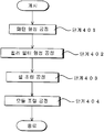
도 23은 본 실시예에 따른 조명 광학 장치의 조정 방법의 각 공정을 개략적으로 나타내는 플로우차트,
도 24는 본 실시예의 변형예에 따른 조정 방법의 각 공정을 개략적으로 나타내는 플로우차트,
도 25는 본 실시예의 전체 시스템을 임의의 소정 각도에서 잘라내어 표현한 것을 도시한 도면,
도 26은 본 실시예의 전체 시스템을 도 25와는 다른 각도에서 잘라내어 표현한 개념도,
도 27은 도 26의 시스템에 있어서 디스플레이 상에 제공되는 사용자 인터페이스 화면의 일례를 도시하는 도면,
도 28은 선광량(이상량) 분포의 일차 성분(경사 성분)만을 보정하는 데에 이용되는 비구면 선광자(이상자)의 구성을 개략적으로 나타내는 도면,
도 29는 마이크로 디바이스로서의 반도체 디바이스를 얻을 때의 방법의 플로우차트,
도 30은 마이크로 디바이스로서의 액정 표시 소자를 얻을 때의 방법의 플로우차트이다.BRIEF DESCRIPTION OF THE DRAWINGS Fig. 1 is a view schematically showing a configuration of an exposure apparatus according to an embodiment of the present invention,
FIG. 2 is a view schematically illustrating an internal configuration of a polarization state measuring unit of FIG. 1;
3 is a diagram schematically showing the configuration of each variable phase difference member according to the present embodiment;
4 schematically shows a configuration of an exposure apparatus according to a first modification;
5 is a view schematically showing the configuration of the variable beneficiation unit according to the first modification,
FIG. 6 is a view schematically showing the configuration of each variable beneficiation member constituting the variable beneficiation unit of FIG. 5;
7 is a diagram illustrating crystal beneficiation;
FIG. 8 is a view schematically showing a circular-shaped secondary light source set to a circumferentially polarized state by the action of the variable beneficiation unit of FIG. 5;
9 is a view schematically showing a ring-shaped secondary light source set to a radially polarized state by the action of the variable beneficiation unit of FIG. 5;
10 schematically shows a configuration of a variable phase difference unit according to the present embodiment;
11 is a diagram schematically illustrating the operation of the variable phase difference unit of FIG. 10;
12 schematically shows a configuration of another variable phase difference unit according to the present embodiment;
FIG. 13 is a diagram schematically illustrating the operation of the variable phase difference unit of FIG. 12; FIG.
14 schematically shows a configuration of a variable beneficiation unit according to a second modification;
15 is a diagram schematically showing a configuration of a variable beneficiation unit according to a modification of the example of FIG. 14;
16 is a diagram schematically showing a configuration of a variable beneficiation / deviation unit according to a third modification;
(A) is a figure which shows the secondary light source of a multipolar shape, (b) is an abnormality of the unit with the variable light flux which forms the secondary light source of the multipolar shape shown to (a). Drawing showing the positional relationship when ejected from the
FIG. 18 is a diagram schematically showing the configuration and operation of a pair of aspherical optoirs according to a fourth modified example; FIG.
FIG. 19 is a diagram schematically showing an example of distribution of beneficiation amount (ideal amount) given to a pair of aspherical beneficiaries (inner box);
20 is a diagram schematically showing another example of the distribution of the amount of beneficiation (ideal amount) imparted to a pair of aspherical beneficiaries (inner box);
21 is a diagram schematically showing a modification using three aspherical beneficiaries (inner box) having a beneficiation amount (ideal amount) distribution in which the beneficiation amount (ideal amount) differs depending on the incident position;
FIG. 22 is a diagram showing cross sections of an on-axis luminous flux and an off-axis luminous flux that pass through an aspherical optical fan (inner box) in the modification of FIG. 21, respectively; FIG.
23 is a flowchart schematically showing each step of the method of adjusting the illumination optical device according to the present embodiment;
24 is a flowchart schematically showing each process of the adjustment method according to the modification of the present embodiment,
25 is a view showing a cut out representation of the entire system of the present embodiment at any predetermined angle;
FIG. 26 is a conceptual view of the entire system of the present embodiment cut out from an angle different from that of FIG. 25;
27 illustrates an example of a user interface screen provided on a display in the system of FIG. 26;
28 is a diagram schematically showing the configuration of an aspherical beneficiator (winner) used to correct only the primary component (inclined component) of the beneficiation amount (ideal amount) distribution;
29 is a flowchart of a method for obtaining a semiconductor device as a micro device;
30 is a flowchart of a method for obtaining a liquid crystal display element as a micro device.
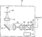
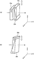
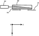
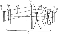
본 발명의 실시예를, 첨부 도면에 근거하여 설명한다. 도 1은, 본 발명의 실시예에 따른 노광 장치의 구성을 개략적으로 나타내는 도면이다. 도 1에 있어서, 감광성 기판인 웨이퍼 W의 법선 방향을 따라서 Z축을, 웨이퍼 W의 면내에 있어서 도 1의 지면에 평행한 방향으로 Y축을, 웨이퍼 W의 면내에 있어서 도 1의 지면에 수직인 방향으로 X축을 각각 설정하고 있다.EMBODIMENT OF THE INVENTION Embodiment of this invention is described based on an accompanying drawing. 1 is a diagram schematically showing a configuration of an exposure apparatus according to an embodiment of the present invention. In Fig. 1, the Z axis along the normal direction of the wafer W as the photosensitive substrate, the Y axis in a direction parallel to the paper surface of Fig. 1 in the plane of the wafer W, and the direction perpendicular to the paper surface of Fig. 1 in the plane of the wafer W. Each of the X axes is set.
도 1을 참조하면, 본 실시예의 노광 장치는, 노광광(조명광)을 공급하기 위한 광원(1)을 구비하고 있다. 광원(1)으로서, 예컨대 193㎚의 파장의 광을 공급하는 ArF 엑시머 레이저 광원이나 248㎚의 파장의 광을 공급하는 KrF 엑시머 레이저 광원 등을 이용할 수 있다. 광원(1)으로부터 사출된 광은, 정형(整形) 광학계(2)에 의해 소요(所要)의 단면 형상의 광속으로 확대되어, 1/4 파장판으로서 기능하는 제 1 가변 위상차 부재(3), 1/2 파장판으로서 기능하는 제 2 가변 위상차 부재(4), 디폴라라이저(depolarizer)(비편광화 소자)(5), 윤대(輪帶) 조명용의 회절 광학 소자(6)를 거쳐서, 어포컬 렌즈(7)에 입사한다.Referring to Fig. 1, the exposure apparatus of the present embodiment includes a
제 1 가변 위상차 부재(3), 제 2 가변 위상차 부재(4) 및 디폴라라이저(5)는 후술하는 바와 같이 편광 상태 전환 수단을 구성하고 있는데, 그 구성 및 작용에 대해서는 후술하기로 한다. 어포컬 렌즈(7)는, 전측(前側) 렌즈군(7a)의 전측 초점 위치와 회절 광학 소자(6)의 위치가 대략 일치하고, 또한 후측(後側) 렌즈군(7b)의 후측 초점 위치와 도면 중 파선(破線)으로 나타내는 소정면(8)의 위치가 대략 일치하도록 설정된 어포컬계(무초점 광학계)이다. 일반적으로, 회절 광학 소자는, 기판에 노광광(조명광)의 파장 정도의 피치를 갖는 단차를 형성함으로써 구성되고, 입사 빔을 소망하는 각도로 회절시키는 작용을 갖는다.The first
구체적으로는, 윤대 조명용의 회절 광학 소자(6)는, 직사각형 형상의 단면을 갖는 평행 광속이 입사한 경우에, 그 파 필드(far field)(또는 프라운호퍼(Fraunhofer) 회절 영역)에 윤대 형상의 광 강도 분포를 형성하는 기능을 갖는다. 따라서, 광속 변환 소자로서의 회절 광학 소자(6)에 입사한 대략 평행 광속은, 어포컬 렌즈(7)의 동공면에 윤대 형상의 광 강도 분포를 형성한 후, 윤대 형상의 각도 분포로 어포컬 렌즈(7)로부터 사출된다. 어포컬 렌즈(7)의 전측 렌즈군(7a)과 후측 렌즈군(7b) 사이의 광로 중에 있어서 그 동공면 또는 그 근방에는, 가변 위상차 유닛(9) 및 원추 액시콘계(10)가 배치되어 있다. 가변 위상차 유닛(9) 및 원추 액시콘계(10)의 구성 및 작용에 대해서는 후술하기로 한다.Specifically, when the parallel light beam having a rectangular cross section is incident, the diffractive
어포컬 렌즈(7)를 거친 광속은, σ값(σ값=조명 광학 장치의 마스크 측 개구수/투영 광학계의 마스크 측 개구수) 가변용의 줌 렌즈(11) 및 가변 선광 유닛(12)을 거쳐서, 마이크로 플라이 아이 렌즈(또는 플라이 아이 렌즈)(13)에 입사한다. 가변 선광 유닛(12)의 구성 및 작용에 대해서는 후술하기로 한다. 마이크로 플라이 아이 렌즈(13)는, 종횡으로, 또한 조밀하게 배열된 다수의 정(正) 굴절력을 갖는 미소 렌즈로 이루어지는 광학 소자이다. 일반적으로, 마이크로 플라이 아이 렌즈는, 예컨대 평행 평면판에 에칭 처리를 실시하여 미소 렌즈군을 형성하는 것에 의해 구성된다.The luminous flux passing through the
여기서, 마이크로 플라이 아이 렌즈를 구성하는 각 미소 렌즈는, 플라이 아이 렌즈를 구성하는 각 렌즈 소자보다도 미소하다. 또한, 마이크로 플라이 아이 렌즈는, 서로 격절(隔絶)된 렌즈 소자로 이루어지는 플라이 아이 렌즈와는 달리, 다수의 미소 렌즈(미소 굴절면)가 서로 격절되는 일 없이 일체적으로 형성되어 있다. 그러나, 정 굴절력을 갖는 렌즈 요소가 종횡으로 배치되어 있다는 점에서 마이크로 플라이 아이 렌즈는 플라이 아이 렌즈와 동일한 파면 분할형의 광학 적분기이다.Here, each micro lens which comprises a micro fly's eye lens is smaller than each lens element which comprises a fly's eye lens. The micro fly's eye lens is formed integrally without a large number of microlenses (microscopic refractive surfaces) being separated from each other, unlike the fly's eye lens composed of lens elements that are separated from each other. However, the micro fly's eye lens is the same wavefront split type optical integrator as the fly's eye lens in that the lens elements having positive refractive power are arranged in the longitudinal direction.
소정면(8)의 위치는 줌 렌즈(11)의 전측 초점 위치의 근방에 배치되고, 마이크로 플라이 아이 렌즈(13)의 입사면은 줌 렌즈(11)의 후측 초점 위치의 근방에 배치되어 있다. 바꿔 말하면, 줌 렌즈(11)는, 소정면(8)과 마이크로 플라이 아이 렌즈(13)의 입사면을 실질적으로 퓨리에 변환의 관계로 배치하고, 나아가서는 어포컬 렌즈(7)의 동공면과 마이크로 플라이 아이 렌즈(13)의 입사면을 광학적으로 대략 공역으로 배치하고 있다. 가변 선광 유닛(12)은, 마이크로 플라이 아이 렌즈(13)의 직전에 배치되고, 나아가서는 어포컬 렌즈(7)의 동공면과 광학적으로 대략 공역으로 배치되어 있다.The position of the
따라서, 마이크로 플라이 아이 렌즈(13)의 입사면 상에는, 어포컬 렌즈(7)의 동공면과 마찬가지로, 예컨대 광축 AX를 중심으로 한 윤대 형상의 조야(照野)가 형성된다. 이 윤대 형상의 조야의 전체 형상은, 줌 렌즈(11)의 초점 거리에 의존하여 상사적(相似的)으로 변화한다. 마이크로 플라이 아이 렌즈(13)를 구성하는 각 미소 렌즈는, 마스크 M 상에 있어서 형성해야 할 조야의 형상(나아가서는 웨이퍼 W 상에 있어서 형성해야 할 노광 영역의 형상)과 상사인 직사각형 형상의 단면을 갖는다.Therefore, on the incidence surface of the micro fly's
마이크로 플라이 아이 렌즈(13)에 입사한 광속은 다수의 미소 렌즈에 의해 이차원적으로 분할되고, 그 후측 초점면 또는 그 근방(나아가서는 조명 동공)에는, 입사 광속에 의해서 형성되는 조야와 대략 동일한 광 강도 분포를 갖는 2차 광원, 즉 광축 AX를 중심으로 한 윤대 형상의 실질적인 면광원으로 이루어지는 2차 광원이 형성된다. 마이크로 플라이 아이 렌즈(13)의 후측 초점면 또는 그 근방에 형성된 2차 광원으로부터의 광속은, 빔 스플리터(14a) 및 콘덴서 광학계(15)를 거친 후, 마스크 블라인드(16)를 중첩적으로 조명한다. 빔 스플리터(14a)를 내장하는 편광 모니터(14)의 구성 및 작용에 대해서는 후술하기로 한다.The light beam incident on the micro fly's
이렇게 해서, 조명 시야 조리개로서의 마스크 블라인드(16)에는, 마이크로 플라이 아이 렌즈(13)를 구성하는 각 미소 렌즈의 형상과 초점 거리에 따른 직사각형 형상의 조야가 형성된다. 마스크 블라인드(16)의 직사각형 형상의 개구부(광 투과부)를 거친 광속은, 결상 광학계(17)의 집광 작용을 받은 후, 소정의 패턴이 형성된 마스크 M을 중첩적으로 조명한다. 즉, 결상 광학계(17)는, 마스크 블라인드(16)의 직사각형 형상 개구부의 상(像)을 마스크 M 상에 형성하게 된다.In this way, the
마스크 스테이지 MS 상에 유지된 마스크 M의 패턴을 투과한 광속은, 투영 광학계 PL을 거쳐서, 웨이퍼 스테이지 WS 상에 유지된 웨이퍼(감광성 기판) W 상에 마스크 패턴의 상을 형성한다. 이렇게 해서, 투영 광학계 PL의 광축 AX와 직교하는 평면(XY 평면) 내에 있어서 웨이퍼 스테이지 WS를 이차원적으로 구동 제어하면서, 나아가서는 웨이퍼 W를 이차원적으로 구동 제어하면서 일괄 노광 또는 스캔 노광을 하는 것에 의해, 웨이퍼 W의 각 노광 영역에는 마스크 M의 패턴이 순차적으로 노광된다.The light beam transmitted through the pattern of the mask M held on the mask stage MS forms an image of a mask pattern on the wafer (photosensitive substrate) W held on the wafer stage WS via the projection optical system PL. In this way, by carrying out package exposure or scanning exposure while driving control of the wafer stage WS two-dimensionally in the plane (XY plane) orthogonal to the optical axis AX of the projection optical system PL, and further driving control of the wafer W two-dimensionally. In each exposure area of the wafer W, the pattern of the mask M is sequentially exposed.
또, 윤대 조명용의 회절 광학 소자(6) 대신에, 4극 조명용의 회절 광학 소자(도시하지 않음)를 조명 광로 중에 설정함으로써, 4극 조명을 실시할 수 있다. 4극 조명용의 회절 광학 소자는, 직사각형 형상의 단면을 갖는 평행 광속이 입사한 경우에, 그 파 필드에 4극 형상의 광 강도 분포를 형성하는 기능을 갖는다. 따라서, 4극 조명용의 회절 광학 소자를 거친 광속은, 마이크로 플라이 아이 렌즈(13)의 입사면에, 예컨대 광축 AX를 중심으로 한 4개의 원 형상의 조야로 이루어지는 4극 형상의 조야를 형성한다. 그 결과, 마이크로 플라이 아이 렌즈(13)의 후측 초점면 또는 그 근방에도, 그 입사면에 형성된 조야와 동일한 4극 형상의 2차 광원이 형성된다.In addition, instead of the diffractive
또한, 윤대 조명용의 회절 광학 소자(6) 대신에, 원형 조명용의 회절 광학 소자(도시하지 않음)를 조명 광로 중에 설정함으로써, 통상의 원형 조명을 실시할 수 있다. 원형 조명용의 회절 광학 소자는, 직사각형 형상의 단면을 갖는 평행 광속이 입사한 경우에, 파 필드에 원 형상의 광 강도 분포를 형성하는 기능을 갖는다. 따라서, 원형 조명용의 회절 광학 소자를 거친 광속은, 마이크로 플라이 아이 렌즈(13)의 입사면에, 예컨대 광축 AX를 중심으로 한 원 형상의 조야를 형성한다. 그 결과, 마이크로 플라이 아이 렌즈(13)의 후측 초점면 또는 그 근방에도, 그 입사면에 형성된 조야와 동일한 원 형상의 2차 광원이 형성된다.In addition, instead of the diffractive
또한, 윤대 조명용의 회절 광학 소자(6) 대신에, 다른 복수극 조명용의 회절 광학 소자(도시하지 않음)를 조명 광로 중에 설정함으로써, 여러 가지 복수극 조명(2극 조명, 8극 조명 등)을 실시할 수 있다. 마찬가지로, 윤대 조명용의 회절 광학 소자(6) 대신에, 적당한 특성을 갖는 회절 광학 소자(도시하지 않음)를 조명 광로 중에 설정함으로써, 여러 가지 형태의 변형 조명을 실시할 수 있다.In addition, instead of the diffractive
원추 액시콘계(10)는, 광원 측에서부터 순서대로, 광원 측으로 평면을 향하여, 또한 마스크 측으로 오목 원추 형상의 굴절면을 향한 제 1 프리즘 부재(10a)와, 마스크 측으로 평면을 향하여, 또한 광원 측으로 볼록 원추 형상의 굴절면을 향한 제 2 프리즘 부재(10b)로 구성되어 있다. 그리고, 제 1 프리즘 부재(10a)의 오목 원추 형상의 굴절면과 제 2 프리즘 부재(10b)의 볼록 원추 형상의 굴절면과는, 서로 접촉 가능하도록 상보적으로 형성되어 있다. 또한, 제 1 프리즘 부재(10a) 및 제 2 프리즘 부재(10b) 중 적어도 한쪽의 부재가 광축 AX를 따라 이동 가능하게 구성되고, 제 1 프리즘 부재(10a)의 오목 원추 형상의 굴절면과 제 2 프리즘 부재(10b)의 볼록 원추 형상의 굴절면의 간격이 가변으로 구성되어 있다. 이하, 윤대 형상 또는 4극 형상의 2차 광원에 주목하여, 원추 액시콘계(10)의 작용 및 줌 렌즈(11)의 작용을 설명한다.The
여기서, 제 1 프리즘 부재(10a)의 오목 원추 형상 굴절면과 제 2 프리즘 부재(10b)의 볼록 원추 형상 굴절면이 서로 접촉하고 있는 상태에서는, 원추 액시콘계(10)는 평행 평면판으로서 기능하며, 형성되는 윤대 형상 또는 4극 형상의 2차 광원에 미치는 영향은 없다. 그러나, 제 1 프리즘 부재(10a)의 오목 원추 형상 굴절면과 제 2 프리즘 부재(10b)의 볼록 원추 형상 굴절면을 이간(離間)시키면, 윤대 형상 또는 4극 형상의 2차 광원의 폭(윤대 형상의 2차 광원의 외경(外俓)과 내경(內徑)의 차의 1/2;4극 형상의 2차 광원에 외접하는 원의 직경(외경)과 내접하는 원의 직경(내경)의 차의 1/2)을 일정하게 유지하면서, 윤대 형상 또는 4극 형상의 2차 광원의 외경(내경)이 변화한다. 즉, 윤대 형상 또는 4극 형상의 2차 광원의 윤대비(내경/외경) 및 크기(외경)가 변화한다.Here, in a state where the concave conical refractive surface of the
줌 렌즈(11)는, 윤대 형상 또는 4극 형상의 2차 광원의 전체 형상을 상사적으로 확대 또는 축소하는 기능을 갖는다. 예컨대, 줌 렌즈(11)의 초점 거리를 최소값에서 소정의 값으로 확대시킴으로써, 윤대 형상 또는 4극 형상의 2차 광원의 전체 형상이 상사적으로 확대된다. 바꿔 말하면, 줌 렌즈(11)의 작용에 의해, 윤대 형상 또는 4극 형상의 2차 광원의 윤대비가 변화하는 일 없이, 그 폭 및 크기(외경)가 함께 변화된다. 이와 같이, 원추 액시콘계(10) 및 줌 렌즈(11)의 작용에 의해, 윤대 형상 또는 4극 형상의 2차 광원의 윤대비와 크기(외경)를 제어할 수 있다.The
편광 모니터(14)는, 마이크로 플라이 아이 렌즈(13)와 콘덴서 광학계(15) 사이의 광로 중에 배치된 빔 스플리터(14a)를 구비하고 있으며, 이 빔 스플리터(14a)로의 입사광의 편광 상태를 검지하는 기능을 갖는다. 바꿔 말하면, 편광 모니터(14)의 검지 결과에 근거하여, 마스크 M(나아가서는 웨이퍼 W)으로의 조명광이 소망하는 편광 상태(비편광 상태를 포함하는 개념)로 되어 있는지 여부가 수시로 검출된다.The polarization monitor 14 is provided with the
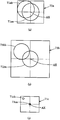
도 2는, 도 1의 편광 상태 측정부의 내부 구성을 개략적으로 나타내는 도면이다. 본 실시예에서는, 도 2에 도시하는 바와 같이 웨이퍼 W를 유지하기 위한 웨이퍼 스테이지 WS에, 웨이퍼 W에 대한 조명광(노광광)의 편광 상태를 측정하기 위한 편광 상태 측정부(18)가 마련되어 있다. 편광 상태 측정부(18)는, 웨이퍼 W의 노광면의 높이 위치에 있어서 이차원적으로 위치 결정 가능한 핀홀 부재(40)를 구비하고 있다. 또, 편광 상태 측정부(18)의 사용시에는, 웨이퍼 W는 광로로부터 퇴피(退避)된다.FIG. 2 is a diagram schematically illustrating an internal configuration of the polarization state measuring unit of FIG. 1. In this embodiment, as shown in FIG. 2, the polarization
핀홀 부재(40)의 핀홀(40a)을 통과한 광은, 콜리메이트 렌즈(41)를 거쳐 대략 평행한 광속으로 되고, 반사경(42)에 의해 반사된 후, 릴레이 렌즈계(43)에 입사한다. 릴레이 렌즈계(43)를 거친 대략 평행한 광속은, 이상자(移相子)로서의 λ/4판(44) 및 편광자로서의 편광 빔 스플리터(45)를 거친 후, 이차원 CCD(46)의 검출면(46a)에 도달한다. 이차원 CCD(46)의 출력은, 제어부(도시하지 않음)에 공급된다. 여기서, λ/4판(44)은, 광축을 중심으로 하여 회전 가능하게 구성되어 있고, 이 λ/4판(44)에는, 그 광축을 중심으로 한 회전각을 설정하기 위한 설정부(47)가 접속되어 있다.The light passing through the
이렇게 해서, 웨이퍼 W에 대한 조명광의 편광도가 0이 아닌 경우에는, 설정부(47)를 거쳐서 λ/4판(44)을 광축 둘레로 회전시키는 것에 의해 이차원 CCD(46)의 검출면(46a)에 있어서의 광 강도 분포가 변화한다. 따라서, 편광 상태 측정부(18)에서는, 설정부(47)를 이용하여 λ/4판(44)을 광축 둘레로 회전시키면서 검출면(46a)에 있어서의 광 강도 분포의 변화를 검출하고, 이 검출 결과로부터 회전 이상자법에 의해 조명광의 편광 상태(편광도;광에 관한 스토크스 파라미터 S1, S2, S3)를 측정할 수 있다.In this way, when the polarization degree of the illumination light with respect to the wafer W is not 0, the
또, 회전 이상자법에 대해서는, 예컨대 츠루타 저(著), 「광의 연필-기술자를 위한 응용 광학」, 주식회사 신기술 커뮤니케이션즈 등에 자세히 기재되어 있다. 실제로는, 핀홀 부재(40)(나아가서는 핀홀(40a))를 웨이퍼면을 따라 이차원적으로 이동시키면서, 웨이퍼면내의 복수의 위치에 있어서의 조명광의 편광 상태를 측정한다. 이 때, 편광 상태 측정부(18)에서는, 이차원적인 검출면(46a)에 있어서의 광 강도 분포의 변화를 검출하기 때문에, 이 검출 분포 정보에 근거하여 조명광의 동공 내에 있어서의 편광 상태의 분포를 측정할 수 있다.In addition, the rotation abnormal magnetic method is described in detail, for example, by Tsuruta, "Applied Optics for Pencils-Engineers", New Technology Communications Co., Ltd., and the like. In practice, the polarization state of the illumination light at a plurality of positions in the wafer surface is measured while moving the pinhole member 40 (the
그런데, 편광 상태 측정부(18)에서는, 이상자로서 λ/4판(44) 대신에 λ/2판을 이용하는 것도 가능하다. 어떠한 이상자를 이용했다고 하더라도, 광의 편광 상태, 즉 광의 4개의 스토크스 파라미터를 측정하기 위해서는, 이상자와 편광자(편광 빔 스플리터(45))의 광축 둘레의 상대 각도를 바꾸거나, 이상자 또는 편광자를 광로로부터 퇴피시키거나 하여, 적어도 4개의 서로 다른 상태에서 검출면(46a)에 있어서의 광 강도 분포의 변화를 검출할 필요가 있다.By the way, in the polarization
또, 본 실시예에서는 이상자로서의 λ/4판(44)을 광축 둘레로 회전시켰지만, 편광자로서의 편광 빔 스플리터(45)를 광축 둘레로 회전시켜도 좋고, 이상자 및 편광자의 쌍방을 광축 둘레로 회전시켜도 좋다. 또한, 이 동작 대신에, 혹은 이 동작에 부가하여, 이상자로서의 λ/4판(44) 및 편광자로서의 편광 빔 스플리터(45) 중의 한쪽 또는 쌍방을 광로로부터 삽탈(揷脫;삽입/분리)시켜도 좋다.In addition, in the present embodiment, the λ / 4
또한, 편광 상태 측정부(18)에서는, 반사경(42)의 편광 특성에 의해 광의 편광 상태가 변화되어 버리는 경우가 있다. 이 경우, 반사경(42)의 편광 특성은 미리 알고 있기 때문에, 소요의 계산에 의해서 반사경(42)의 편광 특성의 편광 상태에의 영향에 근거하여 편광 상태 측정부(18)의 측정 결과를 보정해서, 조명광의 편광 상태를 정확히 측정할 수 있다. 또한, 반사경에 한정되지 않고, 렌즈 등의 다른 광학 부품에 기인하여 편광 상태가 변화되어 버리는 경우에도 마찬가지로 측정 결과를 보정하여, 조명광의 편광 상태를 정확히 측정할 수 있다.In addition, in the polarization
이렇게 해서, 편광 상태 측정부(18)를 이용하여 웨이퍼 W에 대한 조명광의 동공 내에 있어서의 편광 상태(편광도)를 측정하여, 조명광이 동공 내에 있어서 적절한 편광 상태로 되어 있는지 여부가 판정된다. 또, 전술한 실시예에서는, 편광 상태 측정부(18)가 웨이퍼 스테이지 WS에 장착 가능한 구성을 나타내었지만, 이 편광 상태 측정부(18)를 웨이퍼 스테이지 WS에 조립해 넣어도 좋고, 또한 웨이퍼 스테이지 WS와는 별도의 스테이지에 조립해 넣어도 좋다.In this way, the polarization state (polarization degree) in the pupil of the illumination light with respect to the wafer W is measured using the polarization
도 3은, 본 실시예에 따른 각 가변 위상차 부재의 구성을 개략적으로 나타내는 도면이다. 본 실시예에 있어서, 제 1 가변 위상차 부재(3) 및 제 2 가변 위상차 부재(4)는, 도 3(a)에 나타내는 솔레일 보상기로서, 혹은 도 3(b)에 나타내는 바비네 보상기로서 각각 구성되어 있다. 도 3(a)에 나타내는 솔레일 보상기는, 광의 입사 측에서부터 순서대로, 평행 평면판(21a)과, 한 쌍의 편각 프리즘(21b, 21c)으로 구성되어 있다.3 is a diagram schematically showing the configuration of each variable phase difference member according to the present embodiment. In the present embodiment, the first
여기서, 평행 평면판(21a), 제 1 편각 프리즘(21b) 및 제 2 편각 프리즘(21c)은, 복굴절성을 갖는 결정 재료로서의 수정에 의해 형성되어 있다. 또한, 제 1 편각 프리즘(21b)과 제 2 편각 프리즘(21c)은, 서로 보완적인(상보적인) 쐐기 형상의 단면 형상을 갖는다. 또한, 평행 평면판(21a)의 결정 광학축과 한 쌍의 편각 프리즘(21b, 21c)의 결정 광학축이 서로 직교하도록 설정되어 있다.Here, the
또한, 예컨대 마이크로미터 헤드와 같은 구동 수단(도시하지 않음)에 의해, 제 1 편각 프리즘(21b)과 제 2 편각 프리즘(21c)이 Z 방향을 따라서 상대적으로 이동하도록, 혹은 제 1 편각 프리즘(21b)과 제 2 편각 프리즘(21c)이 대향하는 사면(斜面)과 YZ 평면과의 교선(交線) 방향을 따라 상대적으로 이동하도록 구성되어 있다. 도 3(a)에 나타내는 솔레일 보상기(21a∼21c)에서는, 광의 입사 위치에 의존하지 않고, 제 1 편각 프리즘(21b)과 제 2 편각 프리즘(21c)의 상대 위치에 따라서, 입사광과 사출광 사이에 일정한 위상차가 가변적으로 부여된다.Further, for example, by a driving means (not shown) such as a micrometer head, the first and
한편, 도 3(b)에 나타내는 바비네 보상기는, 광의 입사 측에서부터 순서대로, 제 1 편각 프리즘(22a)과, 제 2 편각 프리즘(22b)으로 구성되어 있다. 여기서, 제 1 편각 프리즘(22a) 및 제 2 편각 프리즘(22b)은, 복굴절성을 갖는 결정 재료로서의 수정에 의해 형성되고, 서로 보완적인 쐐기 형상의 단면 형상을 갖는다. 또한, 제 1 편각 프리즘(22a)의 결정 광학축과 제 2 편각 프리즘(22b)의 결정 광학축이 서로 직교하도록 설정되어 있다.On the other hand, the barbine compensator shown in Fig. 3B is composed of a
또한, 예컨대 마이크로미터 헤드와 같은 구동 수단(도시하지 않음)에 의해, 제 1 편각 프리즘(22a)과 제 2 편각 프리즘(22b)이 Z 방향을 따라서 상대적으로 이동하도록, 혹은 제 1 편각 프리즘(22a)과 제 2 편각 프리즘(22b)이 대향하는 사면과 YZ 평면과의 교선 방향을 따라 상대적으로 이동하도록 구성되어 있다. 도 3(b)에 나타내는 바비네 보상기((22a, 22b))에서는, Z 방향에 따른 광의 입사 위치에 어느 정도 의존하지만, 제 1 편각 프리즘(22a)과 제 2 편각 프리즘(22b)의 상대 위치에 따라서, 입사광과 사출광 사이에 대략 일정한 위상차가 가변적으로 부여된다.Further, for example, by a driving means (not shown) such as a micrometer head, the first and
본 실시예에서는, 노광 장치에의 탑재에 앞서 제 1 가변 위상차 부재(3) 단체(單體)에 의해 입사광과 사출광 사이에 부여되는 위상차를 측정하여, 위상차가 광의 파장 λ의 1/4로 되도록, 즉 제 1 가변 위상차 부재(3)가 1/4 파장판으로서 정확하게 기능하도록 미리 조정한다. 마찬가지로, 노광 장치에의 탑재에 앞서 제 2 가변 위상차 부재(4) 단체에 의해 입사광과 사출광 사이에 부여되는 위상차를 측정하고, 위상차가 광의 파장 λ의 1/2로 되도록, 즉 제 2 가변 위상차 부재(4)가 1/2 파장판으로서 정확하게 기능하도록 미리 조정한다.In this embodiment, prior to mounting on the exposure apparatus, the phase difference imparted between the incident light and the emitted light by the first variable
이어서, 1/4 파장판으로서 정확하게 기능하도록 조정된 제 1 가변 위상차 부재(3) 및 1/2 파장판으로서 정확하게 기능하도록 조정된 제 2 가변 위상차 부재(4)를, 정형 광학계(2)와 디폴라라이저(5) 사이의 광로 중의 소정 위치에 각각 위치 결정하고, 광축 AX를 중심으로 하여 일체적으로 회전할 수 있도록 각각 설정한다. 이렇게 해서, 1/4 파장판으로서의 제 1 가변 위상차 부재(3)는, 광축 AX를 중심으로 하여 회전 자유롭게 구성되며, 입사되는 타원 편광의 광을 직선 편광의 광으로 변환한다. 또한, 1/2 파장판으로서의 제 2 가변 위상차 부재(4)는, 광축 AX를 중심으로 하여 회전 자유롭게 구성되어, 입사되는 직선 편광의 편광 방향을 변화시킨다.Subsequently, the first
한편, 디폴라라이저(5)는, 도시를 생략하였지만, 상보적인 형상을 갖는 쐐기 형상의 수정 편각 프리즘과 쐐기 형상의 형석(螢石) 편각 프리즘(또는 석영 편각 프리즘)에 의해 일체적인 프리즘 조립체로서 구성되고, 조명 광로에 대하여 삽탈이 자유롭게 설정되어 있다. 또, 디폴라라이저(5)의 상세한 구성 및 작용에 대해서는, 예컨대 국제 공개 WO 2004/051717호 공보를 참조할 수 있다.On the other hand, although not shown, the
광원(1)으로서 KrF 엑시머 레이저 광원이나 ArF 엑시머 레이저 광원을 이용하는 경우, 이들의 광원으로부터 사출되는 광은 전형적으로는 95% 이상의 편광도를 갖고, 제 1 가변 위상차 부재에는 대략 직선 편광의 광이 입사한다. 그러나, 광원(1)과 제 1 가변 위상차 부재(3) 사이의 광로 중에 이면 반사경으로서의 직각 프리즘이 개재되는 경우, 입사하는 직선 편광의 편광면이 P 편광면 또는 S 편광면에 일치하지 않으면, 직각 프리즘에서의 전(全)반사에 의해 직선 편광이 타원 편광으로 변한다.When the KrF excimer laser light source or the ArF excimer laser light source is used as the
편광 상태 전환 수단(3∼5)에서는, 예컨대 직각 프리즘에서의 전반사에 기인하여 타원 편광의 광이 입사되더라도, 입사하는 타원 편광에 대하여 1/4 파장판으로서의 제 1 가변 위상차 부재(3)를 광축 AX 둘레의 소정의 각도 위치에 설정함으로써, 타원 편광의 입사광이 직선 편광의 광으로 변환되어 제 2 가변 위상차 부재(4)로 도입된다. 또한, 입사하는 직선 편광에 대하여 1/2 파장판으로서의 제 2 가변 위상차 부재(4)를 광축 AX 둘레의 소요의 각도 위치에 설정함으로써, 직선 편광의 입사광이 소망하는 방향으로 편광 방향을 갖는 직선 편광의 광으로 변환되어 디폴라라이저(5)로, 혹은 회절 광학 소자(6)로 직접 도입된다.In the polarization state switching means 3 to 5, even if light of elliptically polarized light is incident due to total reflection in a rectangular prism, for example, the first variable
또한, 디폴라라이저(5)를 조명 광로 중에 삽입하여, 입사하는 직선 편광에 대해 디폴라라이저(5)를 광축 AX 둘레의 소정의 각도 위치에 설정함으로써, 직선 편광의 입사광이 비편광 상태의 광으로 변환(비편광화)되어 회절 광학 소자(6)로 입사한다. 한편, 디폴라라이저(5)가 조명 광로로부터 퇴피되어 있는 경우, 제 2 가변 위상차 부재(4)로부터의 직선 편광의 광은 편광 방향을 바꾸지 않고 그대로 회절 광학 소자(6)에 입사한다.Further, by inserting the
이렇게 해서, 편광 상태 전환 수단(3∼5)에서는, 디폴라라이저(5)를 조명 광로로부터 퇴피시키고, 또한 1/4 파장판으로서의 제 1 가변 위상차 부재(3) 및 1/2 파장판으로서의 제 2 가변 위상차 부재(4)를 광축 AX 둘레의 소정의 각도 위치에 각각 설정함으로써, 소망하는 방향으로 편광 방향을 갖는 직선 편광의 광을 회절 광학 소자(6)에 입사시킬 수 있다. 또한, 1/4 파장판으로서의 제 1 가변 위상차 부재(3) 및 1/2 파장판으로서의 제 2 가변 위상차 부재(4)를 광축 AX 둘레의 소정의 각도 위치에 각각 설정하는 동시에, 디폴라라이저(5)를 조명 광로 중에 삽입하여 광축 AX 둘레의 소정의 각도 위치에 설정함으로써, 비편광 상태의 광을 회절 광학 소자(6)에 입사시킬 수 있다.In this way, in the polarization state switching means 3 to 5, the
바꿔 말하면, 편광 상태 전환 수단(3∼5)에서는, 회절 광학 소자(6)로의 입사광의 편광 상태(나아가서는 마스크 M 및 웨이퍼 W를 조명하는 광의 편광 상태)를 직선 편광 상태와 비편광 상태 사이에서 전환할 수 있다. 또한, 직선 편광 상태의 경우에는, 예컨대 서로 직교하는 편광 상태 사이(Z 방향 편광과 X 방향 편광 사이)에서 전환할 수 있다.In other words, in the polarization state switching means 3 to 5, the polarization state (the polarization state of the light illuminating the mask M and the wafer W) to the diffracted
이상과 같이, 본 실시예에서는, 1/4 파장판이나 1/2 파장판과 같은 파장판을 1장의 수정판에 의해 제조하는 종래 기술과는 달리, 1/4 파장판이나 1/2 파장판과 같은 파장판으로서 기능하는 광학 부재로서, 솔레일 보상기나 바비네 보상기와 같이 입사광과 사출광 사이에 위상차를 가변적으로 부여하는 가변 위상차 부재(3, 4)를 이용하고 있다. 따라서, 가변 위상차 부재(3, 4)를 구성하는 광학 요소(평행 평면판이나 편각 프리즘)에 어느 정도의 제조 오차가 있더라도, 1/4 파장판 및 1/2 파장판으로서 정확하게 기능하도록 각각 조정하고 나서 이용할 수 있다.As described above, in the present embodiment, unlike the prior art in which a wave plate such as a 1/4 wave plate or a 1/2 wave plate is manufactured by one quartz plate, As the optical member functioning as the same wave plate, the
따라서, 본 실시예의 조명 광학 장치(1∼17)에서는, 파장판으로서 기능하는 광학 부재(3, 4)를 구성하는 각 광학 요소(21a∼21c;22a, 22b)의 제조 오차의 영향을 실질적으로 받는 일 없이, 소망하는 편광 상태의 광으로 피조사면으로서의 마스크 M을 조명할 수 있다. 그 결과, 본 실시예의 노광 장치(1∼WS)에서는, 피조사면에 설정된 마스크 M을 소망하는 편광 상태의 광으로 조명하는 조명 광학 장치(1∼17)를 이용하여, 적절한 조명 조건을 기초로 양호한 노광을 할 수 있다.Therefore, in the illumination optical devices 1-17 of this embodiment, the influence of the manufacturing error of each
또, 전술한 설명에서는, 가변 위상차 부재(3, 4) 단체에 의한 위상차를 측정하여, 위상차가 소정의 값(광의 파장 λ의 1/4또는 1/2)으로 되도록 미리 조정한 것을 조명 광로 중에 조립해 넣고 있다. 그러나, 이것에 한정되지 않고, 도 4의 제 1 변형예에 도시하는 바와 같이, 가변 위상차 부재(3, 4)를 조명 광로 중에 조립해 넣은 후에, 편광 상태 측정부(18)의 측정 결과에 근거하여, 가변 위상차 부재(3, 4)가 1/4 파장판 및 1/2 파장판으로서 정확하게 기능하도록 각각 조정하는 것도 가능하다. 또한, 1/4 파장판 및 1/2 파장판으로서 정확하게 기능하도록 조정된 상태로부터 가변 위상차 부재(3, 4)를 더욱 적극적으로 각각 미조정(微調整)함으로써, 다양한 편광 상태의 광으로 피조사면으로서의 마스크 M을, 나아가서는 웨이퍼 W를 조명하는 것도 가능하다.In addition, in the above description, the phase difference by the variable
도 4에 있어서, 제어부 CR은, 편광 상태 측정부(18)로부터의 측정 결과를 수취하여, 가변 위상차 부재(3, 4) 중의 광학 요소(21a∼21c;22a, 22b) 간의 상대 위치를 변경하는 구동부 DR3을 제어하고, 피조사면으로서의 마스크 M 또는 웨이퍼 W 상에서의 편광 상태가 소망하는 상태로 되도록, 가변 위상차 부재(3, 4)에 의한 위상차량을 조정한다.In FIG. 4, the control part CR receives the measurement result from the polarization
또한, 전술한 설명에서는, 가변 위상차 부재(3, 4)를 구성하는 각 광학 요소를 수정에 의해 형성하고 있지만, 이것에 한정되지 않고, 예컨대 불화마그네슘이나 방해석(方解石)과 같은 복굴절성의 결정 재료를 이용하여 가변 위상차 부재(3, 4)의 각 광학 요소를 형성하는 것도 가능하다.In addition, in the above description, although each optical element which comprises the variable
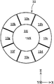
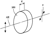
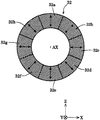
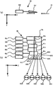
도 5는, 본 실시예에 따른 가변 선광 유닛의 구성을 개략적으로 나타내는 도면이다. 또한, 도 6은, 도 5의 가변 선광 유닛을 구성하는 각 가변 선광 부재의 구성을 개략적으로 나타내는 도면이다. 본 실시예에 따른 가변 선광 유닛(12)은, 마이크로 플라이 아이 렌즈(13)의 직전에, 즉 조명 광학계(2∼17)의 동공 또는 그 근방에 배치되어 있다. 따라서, 윤대 조명의 경우, 가변 선광 유닛(12)에는 광축 AX를 중심으로 한 대략 윤대 형상의 단면을 갖는 광속이 입사되게 된다.5 is a diagram schematically showing the configuration of the variable beneficiation unit according to the present embodiment. 6 is a figure which shows roughly the structure of each variable beneficiation member which comprises the variable beneficiation unit of FIG. The
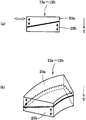
도 5를 참조하면, 가변 선광 유닛(12)은, 광축 AX를 중심으로 하는 원의 둘레 방향을 따라 배치된 8개의 가변 선광 부재(12a, 12b, 12c, 12d, 12e, 12f, 12g, 12h)에 의해 구성되어 있다. 각 가변 선광 부재(12a∼12h)는, 광축 AX를 중심으로 한 윤대 형상의 영역을 원주 방향으로 8등분하여 얻어지는 부채꼴 형상의 외형을 가지며, 또한 서로 동일한 기본 구성을 갖는다. 도 6을 참조하면, 각 가변 선광 부재(12a∼12h)는, 선광성을 갖는 광학 재료로서의 수정에 의해 형성된 한 쌍의 편각 프리즘(23a, 23b)으로 구성되어 있다.Referring to FIG. 5, the
제 1 편각 프리즘(23a)과 제 2 편각 프리즘(23b)은 서로 보완적인 쐐기 형상의 단면 형상을 갖고, 제 1 편각 프리즘(23a)의 결정 광학축 및 제 2 편각 프리즘(23b)의 결정 광학축이 모두 광축 AX에 평행하게(즉, Y 방향에 평행하게) 되도록 배치되어 있다. 또한, 예컨대 마이크로미터 헤드와 같은 구동 수단(도시하지 않음)에 의해, 제 1 편각 프리즘(23a)과 제 2 편각 프리즘(23b)이 광축 AX를 중심으로 하는 원의 직경 방향을 따라서 상대적으로 이동하도록, 혹은 제 1 편각 프리즘(23a)과 제 2 편각 프리즘(23b)이 대향하는 사면과 광축 AX를 포함하는 평면과의 교선 방향을 따라 상대적으로 이동하도록 구성되어 있다.The
이렇게 해서, 도 6에 나타내는 각 가변 선광 부재(12a∼12h)에서는, 제 1 편각 프리즘(23a)과 제 2 편각 프리즘(23b)의 상대 위치에 따라서, 입사하는 직선 편광에 선광 각도가 가변적으로 부여된다. 이하, 도 7을 참조하여, 수정의 선광성에 대하여 간단히 설명한다. 도 7을 참조하면, 두께 d의 수정으로 이루어지는 평행 평면판 형상의 광학 부재(100)가, 그 결정 광학축과 광축 AX가 일치하도록 배치되어 있다. 이 경우, 광학 부재(100)의 선광성에 의해, 입사된 직선 편광의 편광 방향이 광축 AX 둘레로 θ만큼 회전한 상태로 사출된다.In this way, in each of the
이 때, 광학 부재(100)의 선광성에 의한 편광 방향의 회전각(선광 각도) θ는, 광학 부재(100)의 두께 d와 수정의 선광능(旋光能) ρ에 의해, 다음 식 a로 나타낼 수 있다.At this time, the rotation angle (reflection angle) θ of the polarization direction due to the beneficiation of the
![]()
![]()
일반적으로, 수정의 선광능 ρ는, 파장 의존성(사용광의 파장에 의존하여 선광능의 값이 서로 다른 성질:선광 분산)이 있어, 구체적으로는 사용광의 파장이 짧아지면 커지는 경향이 있다. 「응용 광학 Ⅱ」의 제 167 페이지의 기술에 따르면, 250.3㎚의 파장을 갖는 광에 대한 수정의 선광능 ρ는, 153.9도/㎜이다.In general, the crystal beneficiation ρ has a wavelength dependence (property with different values of the beneficiation ability depending on the wavelength of the use light: ray beneficiation), and in particular, tends to increase when the wavelength of the use light becomes short. According to the description on page 167 of "Applied Optics II", the linear light-optical power p of the crystal | crystallization with respect to the light which has a wavelength of 250.3 nm is 153.9 degrees / mm.
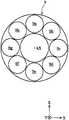
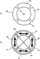
도 8은, 도 5의 가변 선광 유닛의 작용에 의해 둘레 방향 편광 상태로 설정된 윤대 형상의 2차 광원을 개략적으로 나타내는 도면이다. 본 실시예에 있어서, 광축 AX를 사이에 두고 대향하는 가변 선광 부재(12a, 12e)는, Z 방향으로 편광 방향을 갖는 직선 편광의 광이 입사한 경우, Z 방향을 Y축 둘레로 +90도 회전시킨 방향, 즉 X 방향으로 편광 방향을 갖는 직선 편광의 광을 사출하도록 제 1 편각 프리즘(23a)과 제 2 편각 프리즘(23b)의 상대 위치가 설정되어 있다. 따라서, 이 경우, 도 8에 나타내는 윤대 형상의 2차 광원(31) 중, 가변 선광 부재(12a, 12e)의 선광 작용을 받은 광속이 형성하는 한 쌍의 부채꼴 영역(또는 원호 형상 영역)(31a, 31e)을 통과하는 광속의 편광 방향은 X 방향으로 된다.FIG. 8 is a diagram schematically showing a ring-shaped secondary light source set to a circumferentially polarized state by the action of the variable beneficiation unit of FIG. 5. In the present embodiment, the
광축 AX를 사이에 두고 대향하는 가변 선광 부재(12b, 12f)는, Z 방향으로 편광 방향을 갖는 직선 편광의 광이 입사한 경우, Z 방향을 Y축 둘레로 +135도 회전시킨 방향, 즉 Z 방향을 Y축 둘레로 -45도 회전시킨 방향으로 편광 방향을 갖는 직선 편광의 광을 사출하도록 제 1 편각 프리즘(23a)과 제 2 편각 프리즘(23b)의 상대 위치가 설정되어 있다. 따라서, 이 경우, 도 8에 나타내는 윤대 형상의 2차 광원(31) 중, 가변 선광 부재(12b, 12f)의 선광 작용을 받은 광속이 형성하는 한 쌍의 부채꼴 영역(31b, 31f)을 통과하는 광속의 편광 방향은 Z 방향을 Y축 둘레로 -45도 회전시킨 방향으로 된다.The
광축 AX를 사이에 두고 대향하는 가변 선광 부재(12c, 12g)는, Z 방향으로 편광 방향을 갖는 직선 편광의 광이 입사한 경우, Z 방향을 Y축 둘레로 +180도 회전시킨 방향, 즉 Z 방향으로 편광 방향을 갖는 직선 편광의 광을 사출하도록 제 1 편각 프리즘(23a)과 제 2 편각 프리즘(23b)의 상대 위치가 설정되어 있다. 따라서, 이 경우, 도 8에 나타내는 윤대 형상의 2차 광원(31) 중, 가변 선광 부재(12c, 12g)의 선광 작용을 받은 광속이 형성하는 한 쌍의 부채꼴 영역(31c, 31g)을 통과하는 광속의 편광 방향은 Z 방향으로 된다.The
광축 AX를 사이에 두고 대향하는 가변 선광 부재(12d, 12h)는, Z 방향으로 편광 방향을 갖는 직선 편광의 광이 입사한 경우, Z 방향을 Y축 둘레로 +45도 회전시킨 방향으로 편광 방향을 갖는 직선 편광의 광을 사출하도록 제 1 편각 프리즘(23a)과 제 2 편각 프리즘(23b)의 상대 위치가 설정되어 있다. 따라서, 이 경우, 도 8에 나타내는 윤대 형상의 2차 광원(31) 중, 가변 선광 부재(12d, 12h)의 선광 작용을 받은 광속이 형성하는 한 쌍의 부채꼴 영역(31d, 31h)을 통과하는 광속의 편광 방향은 Z 방향을 Y축 둘레로 +45도 회전시킨 방향으로 된다.The
이와 같이, 가변 선광 유닛(12)은, 조명 동공면 또는 그 근방에 배치되어 입사광의 편광 상태를 소정의 편광 상태로 변환하기 위한 편광 변환 소자를 구성하고 있다. 또, 본 실시예에서는, 가변 선광 유닛(12)을 광로로부터 퇴피시키지 않고서 통상의 원형 조명을 실시할 수 있도록, 가변 선광 유닛(12)의 유효 영역의 직경 방향의 크기의 3/10 이상, 바람직하게는 1/3 이상의 크기를 갖고, 또한 선광성을 갖지 않는 원 형상의 중앙 영역(12j)이 마련되어 있다. 여기서, 중앙 영역(12j)은, 예컨대 석영이나 형석과 같이 선광성을 갖지 않는 광학 재료에 의해 형성되어 있어도 좋고, 단순히 원 형상의 개구이더라도 좋다. 단, 중앙 영역(12j)은 가변 선광 유닛(12)에 필수적인 요소는 아니다.Thus, the
본 실시예에서는, 둘레 방향 편광 윤대 조명(윤대 형상의 2차 광원을 통과하는 광속이 둘레 방향 편광 상태로 설정된 변형 조명)에 있어서, 편광 상태 전환 수단(3∼5)의 작용에 의해, Z 방향으로 편광 방향을 갖는 직선 편광의 광을 가변 선광 유닛(12)에 입사시킨다. 그 결과, 마이크로 플라이 아이 렌즈(13)의 후측 초점면 또는 그 근방에는, 도 8에 도시하는 바와 같이, 윤대 형상의 2차 광원(윤대 형상의 조명 동공 분포)(31)이 형성되고, 이 윤대 형상의 2차 광원(31)을 통과하는 광속이 가변 선광 유닛(12)의 작용에 의해 둘레 방향 편광 상태로 설정된다. 둘레 방향 편광 상태에서는, 윤대 형상의 2차 광원(31)을 구성하는 부채꼴 영역(31a∼31h)을 각각 통과하는 광속은, 각 부채꼴 영역(31a∼31h)의 원주 방향에 따른 중심 위치에 있어서의 광축 AX를 중심으로 하는 원의 접선 방향과 대략 일치하는 편광 방향을 갖는 직선 편광 상태로 된다.In the present embodiment, in the circumferentially polarized annular illumination (modified illumination in which the light flux passing through the annular shaped secondary light source is set to the circumferentially polarized state), the Z direction is caused by the action of the polarization state switching means 3 to 5. Thus, light of linearly polarized light having a polarization direction is incident on the
이렇게 해서, 본 실시예에서는, 가변 선광 유닛(12)의 선광 작용에 의해, 광량 손실을 실질적으로 발생시키는 일 없이, 둘레 방향 편광 상태의 윤대 형상의 2차 광원(조명 동공 분포)(31)을 형성할 수 있다. 또, 둘레 방향 편광 상태의 윤대 형상의 조명 동공 분포에 근거하는 둘레 방향 편광 윤대 조명에서는, 최종적인 피조사면으로서의 웨이퍼 W에 조사되는 광이 S 편광을 주성분으로 하는 편광 상태로 된다. 여기서, S 편광이란, 입사면에 대하여 수직인 방향으로 편광 방향을 갖는 직선 편광(입사면에 수직인 방향으로 전기 벡터가 진동하고 있는 편광)을 말한다. 단, 입사면이란, 광이 매질의 경계면(피조사면:웨이퍼 W의 표면)에 도달했을 때에, 그 점에서의 경계면의 법선과 광의 입사 방향을 포함하는 면으로서 정의된다.In this way, in the present embodiment, by the beneficiation of the
그 결과, 둘레 방향 편광 윤대 조명에서는, 투영 광학계 PL의 광학 성능(초점 심도 등)의 향상을 도모할 수 있으며, 웨이퍼(감광성 기판) W 상에 있어서 높은 콘트라스트의 마스크 패턴상을 얻을 수 있다. 즉, 본 실시예의 노광 장치에서는, 광량 손실을 양호하게 억제하면서 둘레 방향 편광 상태의 윤대 형상의 조명 동공 분포를 형성할 수 있는 조명 광학 장치를 이용하고 있기 때문에, 적절한 조명 조건을 기초로 미세 패턴을 충실하게 고(高) 스루풋으로 전사할 수 있다.As a result, in circumferentially polarized circular illumination, the optical performance (focus depth, etc.) of the projection optical system PL can be improved, and a mask pattern image of high contrast can be obtained on the wafer (photosensitive substrate) W. As shown in FIG. That is, in the exposure apparatus of the present embodiment, since the illumination optical apparatus capable of forming a ring-shaped illumination pupil distribution in the circumferentially polarized state while suppressing light loss is favorably used, a fine pattern is selected based on appropriate illumination conditions. Can faithfully transfer at high throughput.
또한, 본 실시예에서는, 편광 상태 전환 수단(3∼5)의 작용에 의해 X 방향으로 편광 방향을 갖는 직선 편광의 광을 가변 선광 유닛(12)에 입사시키고, 도 9에 도시하는 바와 같이 윤대 형상의 2차 광원(32)을 통과하는 광속을 직경 방향 편광 상태로 설정하여, 직경 방향 편광 윤대 조명(윤대 형상의 2차 광원(32)을 통과하는 광속이 직경 방향 편광 상태로 설정된 변형 조명)을 실시할 수 있다. 직경 방향 편광 상태에서는, 윤대 형상의 2차 광원(32)을 구성하는 부채꼴 영역(32a∼32h)을 각각 통과하는 광속은, 부채꼴 영역(32a∼32h)의 원주 방향에 따른 중심 위치에 있어서의 광축 AX를 중심으로 하는 원의 반경 방법과 대략 일치하는 편광 방향을 갖는 직선 편광 상태로 된다.In addition, in this embodiment, light of linearly polarized light having a polarization direction in the X direction is incident on the
직경 방향 편광 상태의 윤대 형상의 조명 동공 분포에 근거하는 직경 방향 편광 윤대 조명에서는, 최종적인 피조사면으로서의 웨이퍼 W에 조사되는 광이 P 편광을 주성분으로 하는 편광 상태로 된다. 여기서, P 편광이란, 전술한 바와 같이 정의되는 입사면에 대하여 평행한 방향으로 편광 방향을 갖는 직선 편광(입사면에 평행한 방향으로 전기 벡터가 진동하고 있는 편광)을 말한다. 그 결과, 직경 방향 편광 윤대 조명에서는, 웨이퍼 W에 도포된 레지스트에 있어서의 광의 반사율을 작게 억제하여, 웨이퍼(감광성 기판) W 상에 있어서 양호한 마스크 패턴상을 얻을 수 있다.In the radially polarized annular illumination based on the annular illumination pupil distribution in the radially polarized state, the light irradiated onto the wafer W as the final irradiated surface becomes a polarized state containing P polarized light as a main component. Here, P-polarized light means linearly polarized light (polarized light in which an electric vector vibrates in a direction parallel to the incident surface) having a polarization direction in a direction parallel to the incident surface defined as described above. As a result, in the radially polarized circular illumination, the reflectance of the light in the resist applied to the wafer W can be suppressed to be small, and a good mask pattern image can be obtained on the wafer (photosensitive substrate) W. FIG.
그런데, 본 출원인은, 예컨대 국제 공개 WO 2005/076045호 팜플렛에 있어서, 조명 동공면 또는 그 근방에 배치되어 입사광의 편광 상태를 소정의 편광 상태로 변환하기 위한 편광 변환 소자로서, 광의 투과 방향에 따른 두께(광축 방향의 길이)가 서로 다른 복수 종류의 수정판을 선광 부재로 하여 원주 방향으로 배치하는 구성을 제안하고 있다. 상기 출원에 있어서 제안된 편광 변환 소자에서는, 입사하는 직선 편광에 소요의 선광 각도를 부여하기 위한 각 선광 부재를 1장의 수정판으로 정밀도 좋게 제조하는 것은 곤란하다. 제조 오차에 기인하여 각 선광 부재가 정확하게 기능하지 않는 경우에는, 소망하는 둘레 방향 편광 상태나 직경 방향 편광 상태 등을 실현할 수가 없다.By the way, in the pamphlet of International Publication No. WO 2005/076045, the present applicant is arranged in the illumination pupil plane or its vicinity and is a polarization conversion element for converting the polarization state of incident light into a predetermined polarization state, The structure which arrange | positions in the circumferential direction using several types of quartz plates from which thickness (length in the optical axis direction) differs as a beneficiation member is proposed. In the polarization conversion element proposed in the said application, it is difficult to manufacture each beneficiation member precisely with one correction plate for giving the beneficiation angle required for linear incidence which is incident. When each beneficiation member does not function correctly due to a manufacturing error, a desired circumferential polarization state, a radial polarization state, etc. cannot be realized.
이에 반하여, 본 실시예에서는, 편광 변환 소자로서의 가변 선광 유닛(12)을, 제 1 편각 프리즘(23a)과 제 2 편각 프리즘(23b)의 상대 위치에 따라 입사하는 직선 편광에 선광 각도를 가변적으로 부여하는 복수의 가변 선광 부재(12a∼12h)에 의해 구성하고 있다. 따라서, 각 가변 선광 부재(12a∼12h)를 구성하는 광학 요소(한 쌍의 편각 프리즘)에 어느 정도의 제조 오차가 있더라도, 소요의 선광 각도를 부여하는 광학 부재로서 정확하게 기능하도록 각 가변 선광 부재(12a∼12h)를 각각 조정하고 나서 가변 선광 유닛(12)을 이용할 수 있다.In contrast, in the present embodiment, the linear beneficiation angle of the
구체적으로는, 노광 장치에의 탑재에 앞서 각 가변 선광 부재(12a∼12h)에 의한 선광 각도를 각각 측정하여, 선광 각도가 소정의 값으로 되도록 각 가변 선광 부재(12a∼12h)(나아가서는 제 1 편각 프리즘(23a)과 제 2 편각 프리즘(23b)의 상대 위치)를 조정하고 나서, 가변 선광 유닛(12)을 조명 광로 중에 조립해 넣는다. 혹은, 가변 선광 유닛(12)을 조명 광로 중에 조립해 넣은 후에, 편광 상태 측정부(18)의 측정 결과에 근거하여, 각 가변 선광 부재(12a∼12h)가 정확하게 기능하도록 제 1 편각 프리즘(23a)과 제 2 편각 프리즘(23b)의 상대 위치를 각각 조정하는 것도 가능하다. 또한, 가변 선광 유닛(12)으로서 정확하게 기능하도록 조정된 상태로부터 각 가변 선광 부재(12a∼12h)를 더욱 적극적으로 각각 미조정함으로써, 다양한 편광 상태(예컨대, 완전한 둘레 방향 편광 상태와 약간 다른 변형 둘레 방향 편광 상태 등)의 광으로 피조사면으로서의 마스크 M을, 나아가서는 웨이퍼 W를 조명하는 것도 가능하다.Specifically, prior to mounting on the exposure apparatus, the beneficiation angles of the
이 경우, 도 1에 도시하는 바와 같이, 제어부 CR은, 편광 상태 측정부(18)로부터의 측정 결과를 수취하여, 가변 선광 유닛(12) 중의 광학 요소(12a∼12h)의 상대 위치를 변경하는 구동부 DR1을 제어하고, 피조사면으로서의 마스크 M 또는 웨이퍼 W 상으로 향하는 광속의 편광 상태가 소망하는 상태로 되도록, 가변 선광 유닛(12)에 의한 선광량의 분포를 조정한다.In this case, as shown in FIG. 1, the control unit CR receives the measurement result from the polarization
이렇게 해서, 본 실시예의 조명 광학 장치(1∼17)에서는, 가변 선광 유닛(12)을 구성하는 각 광학 요소(12a∼12h;23a, 23b)의 제조 오차의 영향을 실질적으로 받는 일 없이, 소망하는 편광 상태의 광으로 피조사면으로서의 마스크 M을 조명할 수 있다. 그 결과, 본 실시예의 노광 장치(1∼WS)에서는, 피조사면에 설정된 마스크 M을 소망하는 편광 상태의 광으로 조명하는 조명 광학 장치(1∼17)를 이용하여, 적절한 조명 조건을 기초로 양호한 노광을 할 수 있다.In this way, in the illumination
또, 전술한 설명에서는, 가변 선광 유닛(12)에 입사하는 광속을, Z 방향으로 편광 방향을 갖는 직선 편광 상태와 X 방향으로 편광 방향을 갖는 직선 편광 상태 사이에서 전환하는 것에 의해, 둘레 방향 편광 윤대 조명과 직경 방향 편광 윤대 조명을 실현하고 있다. 그러나, 이것에 한정되지 않고, 예컨대 Z 방향 또는 X 방향으로 편광 방향을 갖는 직선 편광 상태의 입사 광속에 대하여, 가변 선광 유닛(12)을 도 5에 나타내는 제 1 상태와 광축 AX 둘레로 90도만큼 회전시킨 제 2 상태 사이에서 전환하는 것에 의해, 둘레 방향 편광 윤대 조명과 직경 방향 편광 윤대 조명을 실현하는 것도 가능하다.In addition, in the above description, the circumferentially polarized light is switched by switching the light beam incident on the
또한, 전술한 설명에서는, 마이크로 플라이 아이 렌즈(13)의 직전에 가변 선광 유닛(12)을 배치하고 있다. 그러나, 이것에 한정되지 않고, 일반적으로 조명 광학 장치(1∼PL)의 동공 또는 그 근방에, 예컨대 투영 광학계 PL의 동공 또는 그 근방이나, 결상 광학계(17)의 동공 또는 그 근방이나, 원추 액시콘계(10)의 직전(어포컬 렌즈(7)의 동공 또는 그 근방) 등에 가변 선광 유닛(12)을 배치하는 것도 가능하다.In the above description, the
또한, 전술한 설명에서는, 윤대 형상의 유효 영역의 8분할에 대응하는 8개의 부채꼴 형상의 가변 선광 부재(12a∼12h)에 의해 가변 선광 유닛(12)을 구성하고 있다. 그러나, 이것에 한정되지 않고, 예컨대 원 형상의 유효 영역의 8분할에 대응하는 8개의 부채꼴 형상의 가변 선광 부재에 의해, 혹은 원 형상 또는 윤대 형상의 유효 영역의 4분할에 대응하는 4개의 부채꼴 형상의 가변 선광 부재에 의해, 혹은 원 형상 또는 윤대 형상의 유효 영역의 16분할에 대응하는 16개의 부채꼴 형상의 가변 선광 부재에 의해 가변 선광 유닛(12)을 구성하는 것도 가능하다. 즉, 가변 선광 유닛(12)의 유효 영역의 형상, 유효 영역의 분할수(가변 선광 부재의 수) 등에 대하여 여러 가지 변형예가 가능하다.In addition, in the above-mentioned description, the
또한, 전술한 설명에서는, 수정을 이용하여 각 가변 선광 부재(12a∼12h)(나아가서는 가변 선광 유닛(12))를 형성하고 있다. 그러나, 이것에 한정되지 않고, 선광성을 갖는 다른 적당한 광학 재료를 이용하여 각 가변 선광 부재를 형성하는 것도 가능하다. 이 경우, 사용 파장의 광에 대하여 100도/㎜ 이상의 선광능을 갖는 광학 재료를 이용하는 것이 바람직하다. 즉, 선광능이 작은 광학 재료를 이용하면, 편광 방향의 소요 회전각을 얻기 위해 필요한 두께가 너무 커져서, 광량 손실의 원인이 되기 때문에 바람직하지 못하다.In addition, in the above description, each
또한, 전술한 설명에 있어서, 가변 선광 유닛(12)을 조명 광로에 대하여 고정적으로 마련하였지만, 이 가변 선광 유닛(12)을 조명 광로에 대하여 삽탈 가능하게 마련하여도 좋다. 또한, 전술한 설명에서는, 웨이퍼 W에 대한 S 편광과 윤대 조명을 조합한 예를 나타내었지만, 웨이퍼 W에 대한 S 편광과 2극이나 4극이나 8극 등의 다극 조명 및 원형 조명을 조합하여도 좋다.In addition, although the
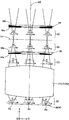
도 10은, 본 실시예에 따른 가변 위상차 유닛의 구성을 개략적으로 나타내는 도면이다. 본 실시예에 따른 가변 위상차 유닛(9)은, 어포컬 렌즈(7)의 동공면 또는 그 근방에, 즉 조명 광학계(2∼17)의 동공 또는 그 근방에 배치되어 있다. 따라서, 윤대 조명의 경우, 가변 위상차 유닛(9)에는, 광축 AX를 중심으로 한 대략 윤대 형상의 단면을 갖는 광속이 입사하게 된다. 또한, 8극 조명의 경우, 가변 위상차 유닛(9)에는, 예컨대 광축 AX를 중심으로 한 8개의 대략 원 형상의 단면을 갖는 광속이 입사하게 된다. 이하, 설명을 단순화하기 위하여 8극 조명의 경우에 대해 설명한다.10 is a diagram schematically showing a configuration of a variable phase difference unit according to the present embodiment. The variable
도 10을 참조하면, 가변 위상차 유닛(9)은, 광축 AX를 중심으로 하는 원의 둘레 방향을 따라 배치된 8개의 원 형상의 가변 위상차 부재(9a, 9b, 9c, 9d, 9e, 9f, 9g, 9h)에 의해 구성되어 있다. 각 가변 위상차 부재(9a∼9h)는, 서로 동일한 기본 구성을 갖고, 구체적으로는 도 3(a)에 나타내는 솔레일 보상기로서, 혹은 도 3(b)에 나타내는 바비네 보상기로서 각각 구성되어 있다.Referring to FIG. 10, the variable
또한, 각 가변 위상차 부재(9a∼9h)는, 예컨대 원 형상의 외형의 중심을 지나 광축 AX에 평행한(Y 방향에 평행한) 축선을 중심으로 하여 회전 자유롭게 구성되어 있다. 일례로서 전술한 둘레 방향 편광 상태로 8극 조명을 실시하는 경우, 도 11에 도시하는 바와 같이 편광 상태 전환 수단(3∼5)의 작용에 의해, 가변 위상차 유닛(9)에 입사하는 8극 형상의 광속(33)을 구성하는 8개의 원 형상의 광속(33a∼33h)은 모두 Z 방향으로 편광 방향을 갖는 직선 편광인 것이다.In addition, each of the variable
그러나, 제 2 가변 위상차 부재(4)와 가변 위상차 유닛(9) 사이의 광로 중에 배치된 광학 부재의 편광 특성 등의 영향에 의해, 가변 위상차 유닛(9)에 도달하는 광속의 편광 상태가 Z 방향으로 편광 방향을 갖는 직선 편광 상태로부터 변화하는 경우가 있다. 단순한 구체예로서, 도 11에 도시하는 바와 같이, 예컨대 가변 위상차 유닛(9)의 가변 위상차 부재(9a)에 입사하는 원 형상의 광속(33a)이 타원 편광 상태로 되거나, 가변 위상차 부재(9h)에 입사하는 원 형상의 광속(33h)이 Z 방향에 대하여 기울어진 방향으로 편광 방향을 갖는 직선 편광 상태로 되거나 한다.However, due to the influence of the polarization characteristics of the optical member disposed in the optical path between the second variable
이 경우, 본 실시예의 가변 위상차 유닛(9)에서는, 가변 위상차 부재(9a)가 1/4 파장판으로서 정확하게 기능하도록, 제 1 편각 프리즘(21b)과 제 2 편각 프리즘(21c)의 상대 위치(혹은 제 1 편각 프리즘(22a)과 제 2 편각 프리즘(22b)의 상대 위치)를 조정한다. 또한, 가변 위상차 부재(9h)가 1/2 파장판으로서 정확하게 기능하도록, 제 1 편각 프리즘(21b)과 제 2 편각 프리즘(21c)의 상대 위치(혹은 제 1 편각 프리즘(22a)과 제 2 편각 프리즘(22b)의 상대 위치)를 조정한다.In this case, in the variable
이어서, 가변 위상차 부재(9a)를 중심 축선 둘레의 소정의 각도 위치에 설정함으로써, 타원 편광의 입사광을 Z 방향으로 편광 방향을 갖는 직선 편광의 광으로 변환한다. 또한, 가변 위상차 부재(9h)를 중심 축선 둘레의 소정의 각도 위치에 설정함으로써, 직선 편광의 입사광을 Z 방향으로 편광 방향을 갖는 직선 편광의 광으로 변환한다. 이렇게 하여, 조명 동공면 또는 그 근방에 배치된 편광 변환 소자로서의 가변 위상차 유닛(9)의 작용에 의해, 입사광의 편광 상태를 소망하는 편광 상태(구체예에서는 Z 방향으로 편광 방향을 갖는 직선 편광 상태)로 변환할 수 있으며, 나아가서는 소망하는 편광 상태(예컨대, 둘레 방향 편광 상태, 직경 방향 편광 상태, Z 방향으로 편광 방향을 갖는 직선 편광 상태 등)로 마스크 M 및 웨이퍼 W를 조명할 수 있다. 즉, 본 실시예에 따른 가변 위상차 유닛(9)을 이용하여, 조명 동공면 또는 그 근방의 위치에서의 편광 상태를 국소적으로 변경함으로써, 조명 동공면 또는 그 근방에 있어서 소망하는 편광 상태의 분포를 갖는 조명광으로 마스크 M 및 웨이퍼 W를 조명할 수 있으며, 나아가서는 소망하는 해상도나 초점 심도 향상의 효과를 얻을 수 있을 뿐만 아니라, 예컨대 패턴 좌우 방향이나 상하 방향에 있어서의 비대칭 오차의 발생을 억제할 수 있다.Subsequently, by setting the variable
또, 전술한 설명에서는, 8극 조명을 실시하는 경우에 주목하고 있지만, 이것에 한정되지 않고, 예컨대 2극, 4극과 같은 복수극 조명이나, 윤대 조명을 실시하는 경우에도 마찬가지로, 편광 변환 소자로서의 가변 위상차 유닛(9)의 작용에 의해 입사광의 편광 상태를 소망하는 편광 상태로 변환할 수 있다. 또한, 전술한 설명에서는, 가변 위상차 유닛(9)을 어포컬 렌즈(7)의 동공면 또는 그 근방에 배치하고 있지만, 이것에 한정되지 않고, 일반적으로 조명 광학계(2∼17)의 동공면 또는 그 근방에 배치하는 것도 가능하다. 또한, 가변 위상차 유닛(9)을 조명 광로에 대하여 삽탈 자유롭게 마련하여도 좋고, 조명 광로 중에 고정적으로 마련하여도 좋다.In addition, although the above-mentioned description pays attention to the case of performing 8-pole illumination, it is not limited to this, For example, also when performing plural-pole illumination, such as a 2-pole and a 4-pole, or a ring-shaped illumination, it is similar as a polarization conversion element. By the action of the variable
또한, 전술한 설명에서는, 가변 위상차 유닛(9)을 통과한 직후의 8극 형상의 광속(33a∼33h)이 모두 Z 방향으로 편광 방향을 갖는 직선 편광 상태로 되도록 조정하고 있지만, 이것에 한정되지 않고, 가변 위상차 유닛(9)을 통과한 직후의 광속이 여러 가지 편광 상태로 되도록 조정하는 것도 가능하다.In addition, although the above-mentioned description adjusts so that all 8 pole-shaped
또한, 편광 상태 측정부(18)의 측정 결과에 근거하여, 어떤 조정 상태로부터 각 가변 위상차 부재(9a∼9h)를 더욱 적극적으로 각각 미조정함으로써, 더욱 다양한 편광 상태의 광으로 피조사면으로서의 마스크 M을, 나아가서는 웨이퍼 W를 조명하는 것도 가능하다. 이 경우, 제어부 CR은, 도 1에 나타낸 구동부 DR2를 거쳐서 가변 위상차 유닛(9) 중의 각 가변 위상차 부재(9a∼9h)를 조정한다.Further, based on the measurement result of the polarization
또, 도 5에 나타낸 가변 선광 유닛(12)과 도 10에 나타낸 가변 위상차 유닛(9)을 조합하여 이용하여도 좋다. 이 경우, 가변 위상차 유닛(9)에 의해서 조명광의 타원 편광율을 제어하고, 가변 선광 유닛(12)에 의해서 편광 방향(타원 편광의 경우에는 그 장축 방향)을 제어하는 것이 바람직하다. 이 때, 가변 위상차 유닛(9)과 가변 선광 유닛(12)을 인접한 상태로 배치하여도 좋고, 이들 유닛 사이에 릴레이 광학계(7b, 11)를 사이에 두고, 이들의 유닛(9, 12)이 서로 공역으로 되도록 배치하여도 좋다.Alternatively, the
도 12는, 본 실시예에 따른 별도의 가변 위상차 유닛의 구성을 개략적으로 나타내는 도면이다. 도 12에 나타내는 가변 위상차 유닛(19)은, 도 12(a)에 도시하는 바와 같이 마스크 블라인드(16)의 근방에, 즉 조명 광학 장치(1∼17)의 피조사면과 광학적으로 공역인 위치 또는 그 근방에 배치되어 있다. 따라서, 가변 위상차 유닛(19)에는, 윤대 조명이나 복수극 조명이나 원형 조명 등에 의존하지 않고, 마스크 M 상의 조명 영역이나 웨이퍼 W 상의 노광 영역(스캔 노광의 경우에는 정지 노광 영역)과 거의 상사(相似)인 직사각형 형상의 광속이 입사하게 된다.12 is a diagram schematically showing the configuration of another variable phase difference unit according to the present embodiment. The variable
도 12(b)를 참조하면, 가변 위상차 유닛(19)은, 광축 AX를 중심으로 하는 직사각형 형상의 영역 내에 대략 조밀 배치된 다수의 원 형상의 가변 위상차 부재(19a, 19b, 19c, 19d, 19e, …)에 의해 구성되어 있다. 각 가변 위상차 부재(19a∼19e, …)는, 서로 동일한 기본 구성을 갖고, 구체적으로는 도 3(a)에 나타내는 솔레일 보상기로서, 혹은 도 3(b)에 나타내는 바비네 보상기로서 각각 구성되어 있다.Referring to Fig. 12 (b), the
또한, 각 가변 위상차 부재(19a∼19e, …)는, 예컨대 원 형상의 외형의 중심을 지나 광축 AX에 평행한(Y 방향에 평행한) 축선을 중심으로 하여 회전 자유롭게 구성되어 있다. 일례로서 Y 방향으로 편광 방향을 갖는 직선 편광 상태로 마스크 M 및 웨이퍼 W를 조명하는 경우, 도 13에 도시하는 바와 같이 편광 상태 전환 수단(3∼5)의 작용에 의해, 가변 위상차 유닛(19)의 각 가변 위상차 부재(19a∼19e, …)에 입사하는 광속은 모두 Z 방향으로 편광 방향을 갖는 직선 편광인 것이다.In addition, each of the variable
그러나, 제 2 가변 위상차 부재(4)와 가변 위상차 유닛(19) 사이의 광로 중에 배치된 광학 부재의 편광 특성 등의 영향에 의해, 가변 위상차 유닛(19)에 도달하는 광속의 편광 상태가 Z 방향으로 편광 방향을 갖는 직선 편광 상태로부터 변화하는 경우가 있다. 단순한 구체예로서, 도 13에 도시하는 바와 같이, 예컨대 가변 위상차 유닛(19)의 가변 위상차 부재(19a)에 입사하는 광속이 타원 편광 상태로 되거나, 가변 위상차 부재(19e)에 입사하는 광속이 Z 방향에 대하여 기울어진 방향으로 편광 방향을 갖는 직선 편광 상태로 되거나 한다.However, due to the influence of the polarization characteristics of the optical member disposed in the optical path between the second variable
이 경우, 도 12의 가변 위상차 유닛(19)에서는, 가변 위상차 부재(19a)가 1/4 파장판으로서 정확하게 기능하도록, 제 1 편각 프리즘(21b)과 제 2 편각 프리즘(21c)의 상대 위치(혹은 제 1 편각 프리즘(22a)과 제 2 편각 프리즘(22b)의 상대 위치)를 조정한다. 또한, 가변 위상차 부재(19e)가 1/2 파장판으로서 정확하게 기능하도록, 제 1 편각 프리즘(21b)과 제 2 편각 프리즘(21c)의 상대 위치(혹은 제 1 편각 프리즘(22a)과 제 2 편각 프리즘(22b)의 상대 위치)를 조정한다.In this case, in the variable
이어서, 가변 위상차 부재(19a)를 중심 축선 둘레의 소정의 각도 위치에 설정함으로써, 타원 편광의 입사광을 Z 방향으로 편광 방향을 갖는 직선 편광의 광으로 변환한다. 또한, 가변 위상차 부재(19e)를 중심 축선 둘레의 소정의 각도 위치에 설정함으로써, 직선 편광의 입사광을 Z 방향으로 편광 방향을 갖는 직선 편광의 광으로 변환한다. 이렇게 해서, 피조사면과 광학적으로 공역인 위치 또는 그 근방에 배치된 편광 변환 소자로서의 가변 위상차 유닛(19)의 작용에 의해, 입사광의 편광 상태를 소망하는 편광 상태(구체예에서는 Z 방향으로 편광 방향을 갖는 직선 편광 상태)로 변환할 수 있으며, 나아가서는 소망하는 편광 상태(Y 방향으로 편광 방향을 갖는 직선 편광 상태)로 마스크 M 및 웨이퍼 W를 조명할 수 있다. 즉, 본 실시예에 따른 별도의 가변 위상차 유닛(19)을 이용하여, 피조사면(마스크 M, 웨이퍼 W)을 조명하는 광의 편광 상태를 국소적으로 변경함으로써, 피조사면 상에 있어서 소망하는 편광 상태의 분포를 갖는 조명광으로 마스크 M 및 웨이퍼 W를 조명할 수 있으며, 나아가서는 웨이퍼 W 상에 형성되는 패턴의 선폭이 노광 영역 내의 위치마다 분산되는 것을 억제하여, 이른바 필드 내 선폭 차의 발생을 억제할 수 있다.Subsequently, by setting the variable
또, 도 5의 가변 선광 유닛과 도 12의 가변 위상차 유닛, 혹은 도 10의 가변 위상차 유닛과 도 12의 가변 위상차 유닛을 병용하는 것도 가능하다. 이 경우, 조명 동공면 또는 그 근방에서의 편광 상태를 국소적으로 연속 변경하면서 피조사면(마스크 M, 웨이퍼 W)을 조명하는 광의 편광 상태를 국소적으로 연속 변경함으로써, 조명 동공면 또는 그 근방에 있어서 소망하는 편광 상태의 분포를 갖고, 또한 피조사면 상에 있어서 소망하는 편광 상태의 분포를 갖는 조명광으로 마스크 M 및 웨이퍼 W를 조명할 수 있으며, 나아가서는 패턴의 비대칭 오차의 발생 및 필드 내 선폭 차의 발생 등을 억제할 수 있다.Moreover, it is also possible to use together the variable beneficiation unit of FIG. 5, the variable phase difference unit of FIG. 12, or the variable phase difference unit of FIG. In this case, by locally continuously changing the polarization state at or near the illumination pupil plane, locally changing the polarization state of the light illuminating the irradiated surface (mask M, wafer W) to the illumination pupil plane or the vicinity thereof. Mask M and wafer W can be illuminated with illumination light having a distribution of the desired polarization state and having a distribution of the desired polarization state on the irradiated surface, furthermore, the occurrence of pattern asymmetry errors and the line width difference in the field. Generation and the like can be suppressed.
또, 전술한 설명에서는, 가변 위상차 유닛(19)을 마스크 블라인드(16)의 근방에 배치하고 있다. 그러나, 이것에 한정되지 않고, 마스크 블라인드(16)의 근방 이외에, 조명 광학 장치(1∼17)의 피조사면의 근방(예컨대 마스크 M의 근방), 피조사면과 광학적으로 공역인 위치, 또는 해당 공역인 위치의 근방에 배치하는 것도 가능하다. 또한, 가변 위상차 유닛(19)을 조명 광로에 대하여 삽탈 자유롭게 마련하여도 좋고, 조명 광로 중에 고정적으로 마련하여도 좋다. 또, 스캔 노광의 경우에는, 다수의 원 형상의 가변 위상차 부재를 비(非) 스캔 방향을 따라서 배치하는 것이 바람직하고, 또한 비스캔 방향에 따른 배치가 갈지자 형상(혹은 지그재그 형상)으로 되는 것이 바람직하다.In addition, in the above description, the
또한, 전술한 설명에서는, 가변 위상차 유닛(19)을 통과한 직후의 광속이 모두 Z 방향으로 편광 방향을 갖는 직선 편광 상태로 되도록 조정하고 있지만, 이것에 한정되지 않고, 가변 위상차 유닛(19)을 통과한 직후의 광속이 여러 가지 편광 상태로 되도록 조정하는 것도 가능하다. 또한, 편광 상태 측정부(18)의 측정 결과에 근거하여, 어떤 조정 상태로부터 각 가변 위상차 부재(19a∼19e, …)를 더욱 적극적으로 각각 미조정함으로써, 다양한 편광 상태의 광으로 피조사면으로서의 마스크 M을, 나아가서는 웨이퍼 W를 조명하는 것도 가능하다.In addition, in the above-mentioned description, although the luminous flux immediately after passing through the variable
이 경우, 도 12에 도시하는 바와 같이, 제어부 CR은, 편광 상태 측정부(18)로부터의 측정 결과를 수취하여, 가변 위상차 유닛(19) 중의 가변 위상차 부재(19a∼19e)를 구동하는 구동부 DR4를 제어하고, 피조사면으로서의 마스크 M 또는 웨이퍼 W 상에서의 광속의 편광 상태 분포가 소망하는 상태로 되도록, 가변 위상차 유닛(19)에 의한 위상차량의 분포를 조정한다.In this case, as shown in FIG. 12, the control unit CR receives the measurement result from the polarization
또한, 전술한 실시예에서는, 조명 광학 장치(1∼17)의 피조사면과 광학적으로 공역인 위치 또는 그 근방에 가변 위상차 유닛(19)을 배치하고 있지만, 이 가변 위상차 유닛 대신에, 복수의 가변 선광 유닛을 배치하여도 좋다. 이 경우, 각각의 가변 선광 부재의 형상은, 도 5에 나타낸 바와 같은 부채꼴 형상이 아니라, 원 형상인 것이 바람직하다. 이 구성에 의해, 피조사면 상에 있어서 소망하는 편광 방향의 분포를 갖는 조명광으로 직선 편광 조명을 실시할 수 있다. 나아가서는, 피조사면 상에 있어서 소망하는 편광 상태의 분포를 갖는 조명광으로 편광 조명을 실시할 수 있다. 또, 이러한 가변 선광 유닛과 가변 위상차 유닛을 조합하여 이용하여도 좋다. 이 경우, 가변 위상차 유닛에 의해서 조명광의 타원 편광율을 제어하고, 가변 선광 유닛에 의해서 편광 방향(타원 편광의 경우에는 그 장축 방향)을 제어하는 것이 바람직하다.Further, in the above-described embodiment, the variable
또한, 도 14에 제 2 변형예로서 도시하는 바와 같이, 가변 선광 유닛(80)으로서, 비스캔 방향(X 방향)에 대응한 방향을 따라서, 쐐기 형상으로 형성된 선광성을 갖는 광학 재료(예컨대 수정)로 이루어지는 가변 선광 부재(81a∼81f)를 배치하여도 좋다. 이들 가변 선광 부재(81a∼81f)는 스캔 방향에 대응하는 방향(Z 방향)으로 움직일 수 있으며, 그 이동량은, 제어부 CR에 의해 제어되고 각 가변 선광 부재(81a∼81f)에 접속된 구동 유닛(82a∼82f)에 의해 조정된다.In addition, as shown in FIG. 14 as a 2nd modification, the optical material (for example, crystal | crystallization) which has wedge shape formed in the wedge shape along the direction corresponding to the bisscan direction (X direction) as the
도 14(b)를 참조하여, 각 가변 선광 부재(81a∼81f)의 작용에 대하여 설명한다. 또, 여기서는 가변 선광 부재(81f)를 대표로 설명한다. 도 14(b)에 있어서, 가변 선광 부재(81f)의 이동 방향(Z 방향)에 따른 복수의 위치(83f1∼83f5)를 생각한다. 이 때, 마스크 블라인드(16)의 개구부(16a) 내의 복수의 위치(83f1∼83f5)를 통과한 각 광속의 편광 상태를 참조 부호 "84f1∼84f5"로 나타낸다. 가변 선광 부재(81f)를 거치지 않은 광속의 편광 상태(84f1∼84f3)에 대하여, 가변 선광 부재(81f)를 거친 광속의 편광 상태(84f4, 84f5)는, 가변 선광 부재(81f)의 광축 방향(Y 방향)의 두께에 따라서, 입사한 직선 편광의 편광 방향이 광축 둘레로 회전한다.Referring to Fig. 14B, the operation of the
여기서, 스캔 노광을 생각해 보면, 웨이퍼 W 상의 한 점에 도달하는 광속의 편광 상태는, 스캔 방향에 따른 광속군의 평균적인 편광 상태라고 생각할 수 있다. 제 2 변형예에서는, 가변 선광 부재(81f)의 Z 방향 위치에 따라서, Z 방향에 따른 광속의 편광 상태(84f1∼84f5)가 평균적인 편광 상태를 변경할 수 있기 때문에, 웨이퍼 W 상의 한 점에 도달하는 광속의 편광 상태를 변경할 수 있다. 그리고, 비스캔 방향에 따른 각 가변 선광 부재(81a∼81f)의 Z 방향 위치를 각각 변경함으로써, 비스캔 방향에서의 광속의 편광 상태의 분포를 변경할 수 있다. 또, 도 15에 도시하는 바와 같이, 가변 선광 유닛의 각 가변 선광 부재(81a∼81f)에, 광축 보정용의 비정질 재료(예컨대 석영)로 이루어지는 쐐기 형상의 광학 부재(85a∼85f)(도 15에서는 "85f"만 도시함)를 마련하고, 전체로서 평행 평면판 형상으로 하여도 좋다.Here, considering the scanning exposure, it can be considered that the polarization state of the luminous flux reaching one point on the wafer W is an average polarization state of the luminous flux group along the scanning direction. In the second modification, since the polarization states 84f1 to 84f5 of the light beams along the Z direction can change the average polarization state in accordance with the Z direction position of the
도 16은, 제 3 변형예에 따른 가변 선광/이상 유닛의 구성을 개략적으로 나타내는 도면이다. 제 3 변형예는, 가변 선광자를 이용하여 직선 편광의 편광 방향(타원 편광의 장축 방향의 방향)을 제어하면서, 가변 이상자를 이용하여 편광의 타원율을 제어하는 것이다. 도 16(a)에 나타내는 측면도, 도 16(b)에 나타내는 상면도 및 도 16(c)에 나타내는 하면도를 참조하면, 선광자(51∼55)는 각각 결정 광학축이 광축 방향을 향한 수정으로 형성되어 있고, 이상자(61∼66)는 각각 결정 광학축이 광축 직교 방향을 향한 수정으로 형성되어 있다.16 is a diagram schematically showing the configuration of the variable beneficiation / abnormal unit according to the third modification. The third modified example is to control the ellipticity of the polarized light using the variable idealizer while controlling the polarization direction of the linearly polarized light (the direction in the major axis direction of the elliptical polarization) using the variable optical photon. Referring to the side view shown in Fig. 16 (a), the top view shown in Fig. 16 (b) and the bottom view shown in Fig. 16 (c), the
여기서, 선광자(51) 및 이상자(61)는 사각뿔 형상을 하고 있으며, 선광자(52∼55) 및 이상자(62∼65)는 각각(광축을 포함하는 면내에서의) 단면이 쐐기 형상이고 광축 방향에서 보아 4분원 형상을 하고 있다. 또한, 이상자(61∼65)에 있어서의 선광 작용을 제거(cancel)하기 위하여, 이상자(61∼65)의 결정 광학축 방향과 이상자(66)의 결정 광학축 방향은 서로 직교하고 있다. 또한, 선광자(52∼55)는, 선광자(51)에 대하여 광축을 기준으로 하는 반경 방향으로 움직일 수 있도록 마련되어 있으며, 이상자(62∼65)는, 이상자(61)에 대하여 광축을 기준으로 하는 반경 방향으로 움직일 수 있도록 마련되어 있다. 이 때, 선광자(52∼55)는, 사각뿔 형상의 선광자(51)의 사면을 따라 움직일 수 있는 것이 바람직하고, 이상자(62∼65)는, 사각뿔 형상의 이상자(61)의 사면을 따라 움직일 수 있는 것이 바람직하다.Here, the
선광자(52∼55)의 반경 방향의 위치에 따라서, 선광자 전체로서의 광축 방향의 두께가 국소적으로 변경된다. 또한, 이상자(62∼65)의 반경 방향의 위치에 따라서 이상자 전체로서의 광축 방향의 두께가 국소적으로 변경된다. 따라서, 선광자(51, 52) 및 이상자(61, 62, 66)를 통과하는 제 1 광속, 선광자(51, 53) 및 이상자(61, 63, 66)를 통과하는 제 2 광속, 선광자(51, 54) 및 이상자(61, 64, 66)를 통과하는 제 3 광속, 및 선광자(51, 55) 및 이상자(61, 65, 66)를 통과하는 제 4 광속의 각각에 부여하는 선광량 및 이상량을 독립적으로 조정할 수 있으므로, 제 1 ∼제 4 광속의 각각의 편광 상태(편광 방향 및 타원율)를 독립 조정할 수 있다.According to the radial position of the optical beams 52-55, the thickness of the optical axis direction as whole optical beams changes locally. In addition, the thickness in the optical axis direction as the whole idealist is locally changed in accordance with the radial position of the idealist 62-65. Therefore, the first light beam passing through the
또, 이상량을 효과적으로 조정(보정)하기 위해서는, 본 변형예와 같이 가변 이상 유닛(61∼66)의 입사 측에 가변 선광 유닛(51∼55)을 배치하는 것이 바람직하다. 여기서, 가변 이상 유닛(61∼66)의 사출 측에 가변 선광 유닛(51∼55)이 배치되는 경우에는, 가변 이상 유닛(51∼55)의 이상자의 결정축 방위와 이상자(51∼55)에 입사하는 광의 편광 방향이 평행 또는 수직으로 될 가능성이 있어, 이 때에는 입사광에 대하여 이상 작용을 부여할 수 없다. 이 경우에는, 가변 위상 유닛(51∼55)의 이상자(51∼55)의 결정축을 광축 직교 면내에서 임의의 방향으로 회전시키기 위한 이상자 회전 기구를 마련하거나, 서로 다른 방위의 결정축을 갖는 이상자와 교환 가능하도록 마련하는 것이 바람직하다. 이와 같이, 광의 입사 측으로부터 가변 선광 유닛 및 가변 이상 유닛의 순으로 배치하는 것은, 본 변형예뿐만 아니라 후술하는 변형예 및 실시예에 있어서도 유효하다.In order to effectively adjust (correct) the abnormal amount, it is preferable to arrange the
이 가변 선광/이상 유닛(51∼55;61∼66)은, 도 5에 나타낸 가변 선광 유닛(12), 도 10에 나타낸 가변 위상 유닛(9) 대신에, 조명 광학 장치의 동공면 또는 그 근방에 배치할 수 있다. 이 때, 조명 광학 장치의 동공면에 형성되는 2차 광원으로서, 예컨대 도 17(a)에 나타내는 바와 같은 다극 형상의 2차 광원(35a∼35d)을 적용할 수 있다. 이 다극 형상의 2차 광원(35a∼35d)를 형성하는 광속이 가변 이상 유닛(61∼65)의 이상자(62∼65)로부터 사출될 때의 위치 관계를 도 17(b)에 나타낸다. 이 도 17의 예에서는, 2차 광원(35a∼35d)의 원주 방향의 절단선을, 광축을 중심으로 한 방위각으로 10도 이상으로 하고 있다. 이에 따라, 분할된 이상자(선광자)의 경계에 2차 광원(35a∼35d)을 형성하는 광이 가해지지 않도록 할 수 있다. 또한, 도 12에 나타낸 가변 위상차 유닛(19) 대신에, 조명 광학 장치의 피조사면, 해당 피조사면의 근방 또는 그들의 공역면에 배치할 수 있다.These variable beneficiation /
또한, 전술한 예에서는, 4개의 영역을 통과하는 광속에 대한 선광량 및 이상량을 독립 제어하였지만, 영역의 수는 4개에 한정되지 않고, 6개여도 8개여도 몇 개여도 좋다. 여기서, 조명광(노광광)의 파장이 193㎚인 경우, 수정의 선광능은 90도/228㎛이며, 이상량은 180도/7㎛이다. 선광자에 의한 직선 편광 방향의 가변량을, 예컨대 ㅁ20도로 하고, 이상자에 의한 위상 조정량을 ㅁ10도로 할 때, 선광자의 쐐기각을 7.2도로 하면, 선광자(52∼55)에게 요구되는 반경 방향의 스트로크는 ㅁ1㎜이며, 이상자의 쐐기각을 0.35도로 하면, 이상자(62∼65)에 요구되는 반경 방향의 스트로크는 100㎛이다.In addition, in the above-mentioned example, although the amount of beneficiation and abnormal amount with respect to the light beam which pass through four areas were controlled independently, the number of area | regions is not limited to four, and may be six, eight, or some. Here, when the wavelength of illumination light (exposure light) is 193 nm, the linear light ability of crystal | crystallization is 90 degree | times / 228 micrometers, and an ideal amount is 180 degree | times / 7 micrometers. When the variable amount of the linearly polarized light direction by the optical beam is set to 20 °, and the phase adjustment amount by the idealizer is 자 10 °, the wedge angle of the optical beam is 7.2 °, which is required by the
도 18은, 제 4 변형예에 따른 한 쌍의 비구면 선광자의 구성 및 작용을 모식적으로 도시하는 도면이다. 본 변형예에서는, 도 18에 도시하는 바와 같이, 마스크 블라인드(16)의 전측(광원 측)에 제 1 비구면 선광자쌍(58)이 배치되고, 마스크 블라인드(16)의 후측(마스크 측)에 제 2 비구면 선광자쌍(59)이 배치되어 있다. 제 1 비구면 선광자쌍(58)은, YZ 단면이 오목형인 선광자(58a)와 당해 선광자(58a)의 오목면과 상보적인 볼록면을 갖는 광축 보정판(58b)과의 조합을 갖고, 제 2 비구면 선광자쌍(59)은, YZ 단면이 볼록 형상의 선광자(59a)와 당해 선광자(59a)의 볼록면과 상보적인 오목면을 갖는 광축 보정판(59b)과의 조합을 갖는다. 이들 제 1 비구면 선광자쌍(58) 및 제 2 비구면 선광자쌍(59)에서는, 광속의 입사 위치에 따라서 선광자의 두께가 서로 다른 구성이다.FIG. 18 is a diagram schematically showing the configuration and operation of a pair of aspherical optical beams according to the fourth modification. In this modification, as shown in FIG. 18, the 1st aspherical
구체적으로, 제 1 비구면 선광자쌍(58)은, 도 19(a)에 도시하는 바와 같이, 예컨대 Y 방향을 따라서 유효 영역의 중심에 있어서 선광량이 가장 작고, 또한 중심으로부터의 거리의 이차 함수에 따라서 선광량이 주변을 향하여 단조롭게 증대되는 것과 같은 2차의 오목 형상 패턴의 선광량 분포를 갖는다. 한편, 제 2 비구면 선광자쌍(59)은, 도 19(b)에 도시하는 바와 같이, 예컨대 Y 방향을 따라서 유효 영역의 중심에 있어서 선광량이 가장 크고, 또한 중심으로부터의 거리의 이차 함수에 따라서 선광량이 주변을 향하여 단조롭게 감소하는 것과 같은 2차의 볼록 형상 패턴의 선광량 분포를 갖는다.Specifically, as shown in Fig. 19A, the first aspherical pair of
그리고, 본 변형예에서는, 제 1 비구면 선광자쌍(58)에 있어서의 유효 영역의 주변에 있어서의 선광량의 최대값과 중심에 있어서의 선광량의 최소값과의 차와, 제 2 비구면 선광자쌍(59)에 있어서의 유효 영역의 중심에 있어서의 선광량의 최대값과 주변에 있어서의 선광량의 최소값과의 차가 같도록 설정되어 있다. 즉, 제 1 비구면 선광자쌍(58)은 2차의 오목 형상 패턴의 선광량 분포를 갖고, 제 2 비구면 선광자쌍(59)은 2차의 볼록 형상 패턴의 선광량 분포를 갖는다. 그 결과, 제 1 비구면 선광자쌍(58)과 제 2 비구면 선광자쌍(59)은 상보적인 선광량 분포를 갖게 된다.In the present modified example, the difference between the maximum value of the amount of beneficiation in the periphery of the effective region in the first
또한, 본 변형예에서는, 제 1 비구면 선광자쌍(58)(엄밀하게는 그 오목면)과 마스크 블라인드(16)와의 거리와, 제 2 비구면 선광자쌍(59)(엄밀하게는 그 볼록면)과 마스크 블라인드(16)와의 거리가 서로 같아지도록 설정되어 있다. 이하, 피조사면으로서의 마스크 M(또는 최종적인 피조사면으로서의 웨이퍼 W) 상에 있어서 광축 AX와 교차하는 중심점 P1에 도달하는 광선, 중심점 P1에서부터 +Y 방향으로 소정 거리만큼 떨어진 점 P2에 도달하는 광선, 및 중심점 P1에서부터 -Y 방향으로 동일한 소정 거리만큼 떨어진 점 P3에 도달하는 광선에 주목한다.In addition, in this modification, the distance between the 1st aspherical photon pair 58 (strictly concave surface) and the
여기서, 2차의 오목 형상 패턴의 선광량 분포를 갖는 제 1 비구면 선광자쌍(58)만이 개재된 경우를 생각해 본다. 도 18에 있어서, 제 1 비구면 선광자쌍(58)과 마스크 블라인드(16) 사이의 3개의 그래프 (A)는, 제 1 비구면 선광자쌍(58)과 마스크 블라인드(16) 사이의 광로를 진행하는, 점 P1, P2, P3에 관한 광속의 각각의 개구 내 선광량의 분포를 나타내는 것이고, 마스크 블라인드(16)와 제 2 비구면 선광자쌍(59) 사이의 3개의 그래프 (B)는, 마스크 블라인드와 제 2 비구면 선광자쌍(59) 사이의 광로를 진행하는, 점 P1, P2, P3에 관한 광속의 각각의 개구 내 선광량의 분포를 나타내는 것이다.Here, the case where only the 1st aspherical
또한, 제 2 비구면 선광자쌍(59)과 결상 광학계(17)(또는 결상 광학계(17)와 투영 광학계 PL) 사이의 3개의 그래프 (C)는, 제 2 비구면 선광자쌍(59)과 결상 광학계(17)(또는 결상 광학계(17)와 투영 광학계 PL) 사이의 광로를 진행하는, 점 P1, P2, P3에 관한 광속의 각각의 개구 내 선광량의 분포를 나타내는 것이며, 결상 광학계(17)(또는 결상 광학계(17)와 투영 광학계 PL)와 피조사면(M, W) 사이의 3개의 그래프 (D)는, 결상 광학계(17)(또는 결상 광학계(17)와 투영 광학계 PL)와 피조사면(M, W) 사이의 광로를 진행하는, 점 P1, P2, P3에 관한 광속의 각각의 개구 내 선광량의 분포를 나타내는 것이다. 이들 그래프 (A)∼(D)에서는, 세로축에 선광량, 가로축에 개구수 NA를 취하고 있다.In addition, three graphs C between the second
여기서, 그래프 (A)로부터, 제 1 비구면 선광자쌍(58)과 마스크 블라인드(16) 사이에 있어서는, 중심점 P1에 관한 개구 내 선광량 분포는 오목 형상 패턴으로 되고, 점 P2에 관한 개구 내 선광량 분포는 경사 패턴으로 되며, 점 P3에 관한 개구 내 선광량 분포는 점 P2의 경사 패턴과는 경사 방향이 반대인 경사 패턴으로 된다. 그래프 (B)에 도시하는 바와 같이, 마스크 블라인드(16)(중간 결상점)를 통과한 후에는, 중심점 P1에 관한 개구 내 선광량 분포는 오목 형상 패턴 그대로지만, 점 P2에 관한 개구 내 선광량 분포와 점 P3에 관한 개구 내 선광량 분포는 경사 방향이 반대 방향인 경사 패턴으로 된다.Here, from the graph (A), between the first aspherical pairs of
또한 제 1 비구면 선광자쌍(58)에 부가하여 2차의 볼록 형상 패턴의 선광량 분포를 갖는 제 2 비구면 선광자쌍(59)도 개재시키면, 제 2 비구면 선광자쌍(59)의 작용에 의해, 도 18의 그래프 (C, D)에 도시하는 바와 같이, 중심점 P1에 관한 선광량 분포가 오목 형상 패턴으로부터 균일한 패턴으로 되돌아가고, 점 P2 및 점 P3에 관한 선광량 분포의 경사 패턴의 정도가 더 조장된 경사 패턴으로 변화한다.In addition to the first
바꿔 말하면, 제 1 보정 비구면 선광자쌍(58)과 제 2 비구면 선광자쌍(59)의 협동 작용에 의해, 중심점 P1(및 P1과 동일한 Y 좌표를 갖는 점)에 관한 선광량 분포가 변화하는 일 없이, 점 P2(및 P2와 동일한 Y 좌표를 갖는 점)에 관한 선광량 분포가 선형적인 경사 패턴으로 변화하고, 점 P3(및 P3과 동일한 Y 좌표를 갖는 점)에 관한 선광량 분포가 점 P2의 경사 패턴과는 경사 방향이 반대이고 경사의 정도가 동등한 선형적인 경사 패턴으로 변화한다. 또, 점 P2 및 점 P3에 관한 선광량 분포의 선형적인 경사 조정의 정도는, 점 P2 및 점 P3의 중심점 P1에서부터의 Y 방향에 따른 거리에 의존한다.In other words, due to the cooperative action of the first corrected
즉, 중심점 P1에서부터 Y 방향을 따라 멀어질수록, 그 점에 관한 선광량 분포의 선형적인 경사 조정의 정도는 커진다. 또한, 도 18을 참조하면 명백하겠지만, 피조사면 상의 각 점에 도달하는 광선이 제 1 비구면 선광자쌍(58) 및 제 2 비구면 선광자쌍(59)을 각각 통과하는 영역(이하, 「파셜(partial) 영역」이라고 함)의 크기는, 제 1 비구면 선광자쌍(58) 및 제 2 비구면 선광자쌍(59)이 마스크 블라인드(16)로부터 멀어질수록 커지고, 각 점에 관한 선광량 분포의 선형적인 경사 조정의 정도도 커진다. 물론, 제 1 비구면 선광자쌍(58) 및 제 2 비구면 선광자쌍(59)의 선광량 분포의 변화의 정도를 더욱 크게 설정하면, 각 점에 관한 선광량 분포의 선형적인 경사 조정의 정도도 커진다.That is, the further away from the center point P1 along the Y direction, the greater the degree of linear inclination adjustment of the beneficiation amount distribution with respect to the point. In addition, as will be apparent with reference to FIG. 18, a region where light rays reaching each point on the irradiated surface pass through the first
또한, 전술한 바와 같이, 본 변형예에서는, 제 1 비구면 선광자쌍(58)과 제 2 비구면 선광자쌍(59)이 상보적인 선광량 분포를 갖고, 제 1 비구면 선광자쌍(58)과 제 2 비구면 선광자쌍(59)이 마스크 블라인드(16)를 사이에 두고 같은 거리에 설정되어 있기 때문에, 피조사면 상의 각 점에 관한 파셜 영역의 위치 및 크기는 제 1 비구면 선광자쌍(58)과 제 2 비구면 선광자쌍(59)에서 대략 일치한다. 그 결과, 제 1 비구면 선광자쌍(58)과 제 2 비구면 선광자쌍(59)의 협동 작용에 의해, 피조사면 상의 각 점에 관한 선광량 분포는 점마다 각각 조정되지만, 피조사면 상의 선광량 분포는 실질적으로 변화하는 일은 없다.In addition, as described above, in the present modification, the first aspherical pair of
이상과 같이, 본 변형예에서는, 제 1 비구면 선광자쌍(58)과 제 2 비구면 선광자쌍(59)이, 피조사면(M, W) 상의 각 점에 관한 선광량 분포를 각각 독립적으로 조정하기 위한 조정 수단, 바꿔 말하면, 본 변형예에서는, 제 1 비구면 선광자쌍(58)과 제 2 비구면 선광자쌍(59)이, 피조사면(M, W) 상의 각 점에 도달하는 광속의 개구 내의 편광 상태를 독립적으로 조정하기 위한 조정 수단을 구성하고 있다. 그 결과, 본 변형예의 노광 장치에서는, 피조사면(M, W)에서의 선광량 분포를 대략 균일하게 유지하면서, 피조사면 상의 각 점에서의 편광 상태 분포를 각각 소망하는 분포로 조정할 수 있기 때문에, 마스크 M의 미세 패턴을 노광 영역의 전체에 걸쳐 소망하는 선폭으로 웨이퍼 W 상에 충실히 전사할 수 있다.As described above, in the present modification, the first aspherical pair of
또, 전술한 설명에서는, 제 1 비구면 선광자쌍(58)과 제 2 비구면 선광자쌍(59)이 마스크 블라인드(16)를 사이에 두고 같은 거리에 설정되어 있지만, 최종적인 피조사면인 웨이퍼 W와 광학적으로 공역인 공역면을 사이에 두고 같은 거리에, 구체적으로는, 예컨대 마스크 M을 사이에 두고 같은 거리에 설정하더라도, 전술한 실시예와 마찬가지의 효과가 얻어진다. 또한, 전술한 설명에서는, 제 1 비구면 선광자쌍(58)이 2차의 오목 형상 패턴의 선광량 분포를 갖고, 또한 제 2 비구면 선광자쌍(59)이 2차의 볼록 형상 패턴의 선광량 분포를 갖지만, 제 1 비구면 선광자쌍(58)이 2차의 볼록 형상 패턴의 선광량 분포를 갖고, 또한 제 2 비구면 선광자쌍(59)이 2차의 오목 형상 패턴의 선광량 분포를 갖는 경우에도 전술한 변형예와 마찬가지의 효과가 얻어진다.In the above description, the first aspheric
또한, 전술한 설명에서는, 제 1 비구면 선광자쌍(58) 및 제 2 비구면 선광자쌍(59)이 소정의 패턴의 선광량 분포를 부여하기 위하여, 예컨대 결정축이 광축과 평행하게 위치 결정된 수정으로 이루어지는 선광자를 이용하였지만, 그 대신에, 예컨대 결정축이 광축과 수직으로 위치 결정된 수정으로 이루어지는 이상자와 광축 보정판을 조합하여, 제 1 비구면 이상자쌍 및 제 2 비구면 이상자쌍을 이용하여도 좋다. 이 경우, 예컨대 제 1 비구면 이상자쌍은, YZ 단면이 오목 형상인 이상자와 당해 이상자의 오목면과 상보적인 볼록면을 갖는 광축 보정판과의 조합을 갖고, 제 2 비구면 이상자쌍은, YZ 단면이 볼록 형상인 이상자와 당해 이상자의 볼록면과 상보적인 오목면을 갖는 광축 보정판과의 조합을 갖는다. 이들 제 1 비구면 이상자쌍 및 제 2 비구면 이상자쌍에서는, 광속의 입사 위치에 따라서 이상자의 두께가 상이한 구성이다.In addition, in the above description, in order to give the distribution of the beneficiation amount of the predetermined pattern to the first
구체적으로, 제 1 비구면 이상자쌍은, 도 19(c)에 도시하는 바와 같이, 예컨대 Y 방향을 따라서 유효 영역의 중심에 있어서 이상량이 가장 작고, 또한 중심으로부터의 거리의 2차 함수에 따라서 이상량이 주변을 향하여 단조롭게 증대되는 것과 같은 2차의 오목 형상 패턴의 이상량 분포를 갖는다. 한편, 제 2 비구면 이상자쌍은, 도 19(d)에 도시하는 바와 같이, 예컨대 Y 방향을 따라서 유효 영역의 중심에 있어서 이상량이 가장 크고, 또한 중심으로부터의 거리의 2차 함수에 따라서 이상량이 주변을 향하여 단조롭게 감소하는 것과 같은 2차의 볼록 형상 패턴의 이상량 분포를 갖는다. 이들 제 1 비구면 이상자쌍과 제 2 비구면 이상자쌍에 의해, 피조사면 상의 각 점에 관한 이상량 분포의 각각을 독립적으로 조정할 수 있다. 바꿔 말하면, 제 1 비구면 이상자쌍과 제 2 비구면 이상자쌍에 의해, 피조사면(M, W) 상의 각 점에 도달하는 광속의 개구 내의 편광 상태를 독립적으로 조정할 수 있다. 또, 이 비구면 이상자쌍과 전술한 비구면 선광자쌍의 쌍방을 조합시켜도 좋다.Specifically, as shown in Fig. 19 (c), the first aspherical pair of abnormalities has the smallest abnormality at the center of the effective area along the Y direction, and the abnormal amount according to the quadratic function of the distance from the center. It has an ideal amount distribution of a secondary concave pattern such as monotonically increasing toward the periphery. On the other hand, as shown in Fig. 19 (d), the second aspherical pair of abnormalities has the largest abnormality at the center of the effective area along the Y-direction, and the abnormal amount according to the quadratic function of the distance from the center. Has an ideal amount distribution of the secondary convex pattern such as monotonically decreasing toward. By these 1st aspherical surface abnormality pair and a 2nd aspherical surface abnormality pair, each of the abnormality distribution about each point on an irradiated surface can be adjusted independently. In other words, the polarization state in the opening of the light beam reaching each point on the irradiated surface M, W can be independently adjusted by the 1st aspherical surface abnormality pair and the 2nd aspherical surface abnormality pair. In addition, you may combine both the aspherical abnormal pair and the above-mentioned aspherical optical pair.
또한, 전술한 설명에서는, 제 1 비구면 선광자(이상자)쌍(58) 및 제 2 비구면 선광자(이상자)쌍(59)이 2차의 패턴의 선광량(이상량) 분포를 갖지만, 이것에 한정되지 않고, 제 1 비구면 선광자(이상자)쌍(58) 및 제 2 비구면 선광자(이상자)쌍(59)에 부여하는 선광량(이상량) 분포의 패턴에 대해서는 여러 가지 변형예가 가능하다. 구체적으로, 예컨대 제 1 비구면 선광자(이상자)쌍(58)이, 도 20(a), (c)에 도시하는 바와 같이, 예컨대 유효 영역의 중심으로부터의 Y 방향에 따른 거리의 4차 함수에 따라서 중심으로부터 주변을 향하여 투과율이 일단 증대된 후에 감소하는 것과 같은 4차의 M자 형상 패턴의 선광량(이상량) 분포를 갖는 변형예도 가능하다.In addition, in the above description, although the first aspherical photon (pair)
이 제 5 변형예에서는, 제 2 비구면 선광자(이상자)쌍(59)은, 도 20(b), (d)에 도시하는 바와 같이 유효 영역의 중심으로부터의 Y 방향에 따른 거리의 4차 함수에 따라서 중심으로부터 주변을 향하여 선광량(이상량)이 일단 감소한 후에 증대되는 것과 같은 4차 W자 형상 패턴의 선광량(이상량) 분포를 갖게 된다. 이 경우, 제 1 비구면 선광자(이상자)쌍(58)의 선광량(이상량) 분포와 제 2 비구면 선광자(이상자)쌍(59)의 선광량(이상량) 분포를 상보적으로 설정하면, 전술한 변형예와 마찬가지의 효과가 얻어진다. 단, 제 1 비구면 선광자(이상자)쌍(58) 및 제 2 비구면 선광자(이상자)쌍(59)이 4차의 패턴의 선광량(이상량) 분포를 갖기 때문에, 선형적인 경사 조정이 아니라 3차 함수적인 경사 조정 효과가 얻어진다. 또, 제 1 비구면 선광자(이상자)쌍(58) 및 제 2 비구면 선광자(이상자)쌍(59)의 패턴의 선광량(이상량) 분포는 4차 이상이어도 좋다.In this fifth modification, the second aspherical photon (pair)
또한, 전술한 설명에서는, 제 1 비구면 선광자(이상자)쌍(58) 및 제 2 비구면 선광자(이상자)쌍(59)에 Y 방향에 따른 일차원의 선광량(이상량) 분포를 부여하고 있는, 즉 선광자(이상자)가 실린드리컬 렌즈 형상이지만, 일차원의 선광량(이상량) 분포의 변화 방향에 대해서는 여러 가지 변형예가 가능하다. 또한, 제 1 비구면 선광자(이상자)쌍(58) 및 제 2 비구면 선광자(이상자)쌍(59)에 이차원적인 선광량(이상량) 분포를 부여하는 것도 가능하다. 또한, 제 1 비구면 선광자(이상자)쌍(58) 및 제 2 비구면 선광자(이상자)쌍(59)에 부여해야 할 선광량(이상량) 분포를 다른 적당한 함수에 따라서 규정하는 것도 가능하다. 일례로서, 예컨대 후술하는 제르니케 다항식을 이용하여 제 1 비구면 선광자(이상자)쌍(58) 및 제 2 비구면 선광자(이상자)쌍(59)의 선광량(이상량) 분포를 규정함으로써, 피조사면 상의 각 점에 관한 개구 내 편광 상태 분포를 다양한 형태에 따라서 점마다 각각 조정하는 것이 가능하게 된다.In addition, in the above-described description, the one-dimensional amount of beneficiation (ideal amount) distribution along the Y direction is given to the first aspherical beneficiary (winner)
그런데, 전술한 변형예에 있어서, 결정축이 광축과 수직하게 위치 결정된 수정으로 이루어지는 이상자를 이용하여 제 1 비구면 이상자쌍과 제 2 비구면 이상자쌍을 구성하였지만, 이상자로서는 수정에 한정되지 않고, 예컨대 불화마그네슘(MgF2) 등의 복굴절성을 나타내는 결정 재료로 형성되는 것이나, 응력 왜곡 분포를 갖는 광 투과성 재료로 형성되는 것이나, 구조 복굴절성을 갖는 패턴을 갖는 광 투과성 재료로 형성되는 것 등 여러 가지의 것을 적용할 수 있다.By the way, in the above-described modification, although the first aspherical pair and the second aspherical pair were formed by using an ideal crystal composed of crystals whose crystal axes were positioned perpendicular to the optical axis, the ideal magnet is not limited to the crystal, for example, magnesium fluoride. It is formed of a crystalline material exhibiting birefringence such as (MgF 2 ), or formed of a light transmissive material having a stress distortion distribution, or formed of a light transmissive material having a pattern having a structure birefringence Applicable
또, 전술한 변형예에서는, 제 1 비구면 선광자(이상자)쌍(58)의 투과율 분포와 제 2 비구면 선광자(이상자)쌍(59)의 선광량(이상량) 분포가 상보적으로 설정되어 있지만, 이것에 한정되지 않고, 제 1 비구면 선광자(이상자)쌍(58)의 선광량(이상량) 분포에 대하여 상보적인 선광량(이상량) 분포와는 실질적으로 다른 선광량(이상량) 분포를 제 2 비구면 선광자(이상자)쌍(59)에 부여하는 변형예도 가능하다. 이 변형예에서는, 제 1 비구면 선광자(이상자)쌍(58)의 선광량(이상량) 분포에 대하여 상보적인 선광량(이상량) 분포와 제 2 비구면 선광자(이상자)쌍(59)의 선광량(이상량) 분포의 차에 따라 피조사면 상의 편광 상태의 분포가 조정되게 되어, 피조사면 상의 편광 상태의 분포를 대략 일정하게 유지하면서, 피조사면 상의 각 점에서의 개구 내에서의 편광 상태의 분포를 각각 대략 균일하게 조정할 수 있다.In addition, in the above-mentioned modification, although the transmittance distribution of the 1st aspherical photon (pair)
마찬가지로, 피조사면 상의 편광 상태의 분포를 적극적으로 조정하는 변형예로서, 마스크 블라인드(16)를 사이에 두고 제 1 비구면 선광자(이상자)쌍(58)과 제 2 비구면 선광자(이상자)쌍(59)을 서로 다른 거리에 설정하는 것도 가능하다. 이 경우, 마스크 블라인드(16)와 제 1 비구면 선광자(이상자)쌍(58)과의 거리와 마스크 블라인드(7)와 제 2 비구면 선광자(이상자)쌍(59)과의 거리와의 차에 따라 피조사면에 있어서의 편광 상태의 분포를 조정할 수 있으며, 나아가서는 피조사면 상의 편광 상태의 분포를 대략 일정하게 유지하면서, 피조사면 상의 각 점에서의 개구 내에서의 편광 상태의 분포를 각각 대략 균일하게 조정할 수 있다.Similarly, as a modification to actively adjust the distribution of the polarization state on the irradiated surface, a pair of first aspherical photon (winner) pairs 58 and a second aspheric photon (winner) pair (with the mask blind 16 interposed therebetween) It is also possible to set 59 at different distances. In this case, the difference between the distance between the
또한, 전술한 설명에서는, 한 쌍의 비구면 선광자(이상자)쌍(58, 59)을 이용하는 것에 의해, 피조사면 상의 편광 상태의 분포를 대략 균일하게 유지 또는 조정하면서 피조사면 상의 각 점에서의 개구 내의 편광 상태의 분포를 각각 대략 균일하게 조정하고 있다. 그러나, 이것에 한정되지 않고, 일반적으로는 소정의 선광량 분포 또는 이상량 분포를 갖는 복수의 비구면 선광자 또는 비구면 이상자로 이루어지는 조정 수단을 이용하여, 본 발명의 효과를 얻을 수 있다. 즉, 조정 수단을 구성하는 비구면 선광자(이상자)의 수 및 배치에 대하여 여러 가지 변형예가 가능하다.In addition, in the above description, by using a pair of aspherical photon (pair) pairs 58 and 59, the opening at each point on the irradiated surface while maintaining or adjusting the distribution of the polarization state on the irradiated surface is approximately uniform. Distribution of the internal polarization state is adjusted to be approximately uniform, respectively. However, it is not limited to this, and generally, the effect of this invention can be acquired using the adjustment means which consists of a some aspherical photon or aspherical abnormality which has predetermined linearity distribution or abnormality distribution. That is, various modifications are possible with respect to the number and arrangement of aspherical beneficiaries (winners) constituting the adjusting means.
구체적으로, 예컨대 도 21에 도시하는 바와 같이, 입사 위치에 따라서 선광량(이상량)이 서로 다른 선광량(이상량) 분포를 갖는 3개의 비구면 선광자(이상자)(71a∼71c)를 이용하는 제 6 변형예도 가능하다. 도 21의 제 6 변형예에서는, 마이크로 플라이 아이 렌즈(13)와 마스크 블라인드(16) 사이의 콘덴서 광학계(15)의 광로 중에 제 1 비구면 선광자(이상자)(71a) 및 제 2 비구면 선광자(이상자)(71b)가 광원 측에서부터 순서대로 배치되고, 콘덴서 광학계(15)와 마스크 블라인드(16) 사이의 광로 중에 제 3 비구면 선광자(이상자)(71c)가 배치되어 있다.Specifically, for example, as shown in FIG. 21, the sixth modification using three aspherical beneficiaries (winners) 71a to 71c having a different amount of beneficiation amount (ideal amount) depending on the incident position. An example is possible. In the sixth modified example of FIG. 21, the first aspherical photon (inner box) 71a and the second aspherical photon (in the optical path of the condenser
이 경우, 도 22에 도시하는 바와 같이, 축상 광속(마스크 블라인드(16)와 광축 AX와의 교점에 도달하는 광속)이 비구면 선광자(이상자)(71a∼71c)를 각각 통과하는 영역, 즉 축상 파셜 영역(71aa, 71ba, 71ca)이 비구면 선광자(이상자)(71a∼71c)마다 다르게 되어 있다. 마찬가지로, 축외 광속(광축 AX로부터 떨어진 마스크 블라인드(16) 상의 점에 도달하는 광속)이 비구면 선광자(이상자)(71a∼71c)를 각각 통과하는 영역, 즉 축외 파셜 영역(71ab, 71bb, 71cb)도 비구면 선광자(이상자)(71a∼71c)마다 다르게 되어 있다.In this case, as shown in FIG. 22, an area in which the axial luminous flux (the luminous flux reaching the intersection between the
이 제 6 변형예에서는, 각 비구면 선광자(이상자)(71a∼71c)의 선광량(이상량) 분포, 각 비구면 선광자(이상자)(71a∼71c)에 있어서의 축상 파셜 영역 및 축외 파셜 영역의 위치 및 크기 등을 적절히 설정함으로써, 피조사면에서의 편광 상태의 분포를 대략 균일하게 조정하면서, 피조사면 상의 각 점에서의 개구 내에서의 편광 상태의 분포를 각각 대략 균일하게 조정할 수 있다. 또한 일반적으로는, 입사 위치에 따라서 선광량(이상량)이 변화하는 소정의 선광량(이상량) 분포를 갖는 복수의 비구면 선광자(이상자)로 이루어지는 조정 수단을 이용하여, 각 비구면 선광자(이상자)의 선광량(이상량) 분포, 각 비구면 선광자(이상자)에 있어서의 축상 파셜 영역 및 축외 파셜 영역의 위치 및 크기 등을 적절히 설정함으로써, 본 발명의 효과를 얻을 수 있다.In this sixth modification, the beneficiation amount (ideal amount) distribution of each aspherical beneficiator (inner box) 71a to 71c, the axial partial region and the off-axis partial region in each aspheric beneficiator (inner box) 71a to 71c By suitably setting a position, a magnitude | size, etc., distribution of the polarization state in the opening in each point on a to-be-irradiated surface can be adjusted substantially uniformly, adjusting the distribution of the polarization state on an irradiated surface substantially uniformly. Moreover, generally, each aspherical beneficiary (winner) is used by the adjustment means which consists of a some aspherical beneficiary (winner) which has a predetermined amount of beneficiation (an abnormal amount) distribution which changes the beneficiary amount (an abnormal amount) according to an incident position. The effect of the present invention can be obtained by appropriately setting the amount of beneficiation (abnormal amount) distribution, the position and size of the axial partial region and the off-axis partial region in each aspherical beneficiary (this box).
이하, 광원(1)에서부터 투영 광학계 PL까지를 피조사면으로서의 웨이퍼 W를 조명하는 조명 광학 장치라고 생각하고, 이 조명 광학 장치(1∼PL)의 조정 방법에 대하여 설명한다. 또, 본 실시예에서는, 조정 방법의 설명을 간소화하기 위하여, 소정의 선광량(이상량) 분포를 갖는 복수(2개 또는 그 이상)의 비구면 선광자(이상자)를 이용하여, 피조사면(웨이퍼 W가 설정되는 면)에서의 편광 상태의 분포를 대략 균일하게 조정하면서, 피조사면 상의 각 점에서의 개구 내에서의 편광 상태의 분포를 각각 대략 균일하게 조정하는 것으로 한다.Hereinafter, it considers the
도 23은, 본 실시예에 따른 조명 광학 장치의 조정 방법의 각 공정을 개략적으로 나타내는 플로우차트이다. 도 23에 도시하는 바와 같이, 본 실시예에 따른 조명 광학 장치(1∼PL)의 조정 방법에서는, 피조사면 상의 복수 점에 관한 개구 내에서의 편광 상태의 분포(동공 편광 상태 분포) 및 피조사면에 있어서의 편광 상태의 분포를 얻는다(S11). 구체적으로, 분포 획득 공정 S11에서는, 조명 광학 장치(1∼PL)의 설계 데이터에 근거하여, 피조사면 상의 복수 점에 관한 개구 내에서의 편광 상태의 분포 및 피조사면에 있어서의 편광 상태의 분포를 산출한다.23 is a flowchart schematically showing each step of the adjusting method of the illumination optical device according to the present embodiment. As shown in FIG. 23, in the adjustment method of the illumination optical apparatus 1-PL which concerns on a present Example, the distribution (polarized-polarization state distribution) of the polarization state in the opening with respect to the several point on an irradiation surface, and an irradiation surface Distribution of the polarization state in is obtained (S11). Specifically, in distribution acquisition process S11, based on the design data of illumination optical apparatus 1-PL, the distribution of the polarization state in the opening with respect to the several point on a to-be-irradiated surface, and the distribution of the polarization state in a to-be-irradiated surface is shown. Calculate.
여기서, 조명 광학 장치(1∼PL)의 설계 데이터로서, 예컨대 마이크로 플라이 아이 렌즈(13)의 직후부터 웨이퍼 W의 직전까지의 광학계(15∼PL)의 데이터, 즉 각 광학면의 곡률 반경, 각 광학면의 축상 간격, 각 광학 부재를 형성하는 광학 재료의 굴절률 및 종류, 사용광의 파장, 각 광학 부재의 선광량(이상량), 반사 방지막이나 반사막의 입사 각도 특성(선광량이나 이상(리타데이션)량) 등의 데이터를 이용한다. 또, 설계 데이터에 근거하여 피조사면 상의 복수 점에 관한 개구 내에서의 편광 상태의 분포를 산출하는 방법에 대해서는, 예컨대 미국 특허 제 6,870,668 호 공보를 참조할 수 있다.Here, as design data of the illumination
혹은, 분포 획득 공정 S11에 있어서, 실제로 제조된 장치마다 피조사면 상의 복수 점에 관한 개구 내에서의 편광 상태의 분포 및 피조사면에 있어서의 편광 상태의 분포를 측정하여도 좋다. 구체적으로, 피조사면 상의 복수 점에 관한 개구 내에서의 편광 상태의 분포 및 피조사면에 있어서의 편광 상태의 분포는, 예컨대 도 2에 나타낸 편광 상태 측정부(18)를 이용하여 측정할 수 있다.Or in distribution acquisition process S11, you may measure the distribution of the polarization state in the opening with respect to the several point on a to-be-irradiated surface, and the distribution of the polarization state in an irradiated surface for every apparatus actually manufactured. Specifically, the distribution of the polarization state in the opening about the plurality of points on the irradiated surface and the distribution of the polarization state on the irradiated surface can be measured using the polarization
본 실시예에서는, 피조사면 상의 복수 점에 관한 개구 내(피조사면 상의 복수 점의 각각에 대한 동공 내)에서의 편광 상태 분포로서, 스토크스 파라미터(S0, S1, S2, S3)에 의해 규정되는 특정 편광도(DSP1, DSP2, DSP3)의 분포를 이용할 수 있다. 여기서, 특정 편광도 DSP1은 동공 상의 한 점을 통과하여 상면(像面) 상의 한 점에 도달하는 광선에 관한 스토크스 파라미터 S0에 대한 스토크스 파라미터 S1의 비(比) S1/S0으로 표시된다. 마찬가지로 특정 편광도 DSP2는 동공 상의 한 점을 통과하여 상면 상의 한 점에 도달하는 광선에 관한 스토크스 파라미터 S0에 대한 스토크스 파라미터 S2의 비 S2/S0으로 표시되며, 특정 편광도 DSP3은 동공 상의 한 점을 통과하여 상면 상의 한 점에 도달하는 광선에 관한 스토크스 파라미터 S0에 대한 스토크스 파라미터 S3의 비 S3/S0으로 표시된다. 여기서, S0은 전(全) 강도이고, S1은 (수평 직선 편광 강도-수직 직선 편광 강도)이며, S2는 (45도 직선 편광 강도-135도 직선 편광 강도)이며, S3은 (우회전 원 편광 강도-좌회전 원 편광 강도)이다.In this embodiment, the Stokes parameters S 0 , S 1 , S 2 , and S 3 as polarization state distributions in the openings (in the pupils to each of the plurality of points on the irradiated surface) with respect to the plurality of points on the irradiated surface. The distribution of specific polarization degrees DSP 1 , DSP 2 , DSP 3 defined by. Here, the specific polarization degree DSP 1 is the ratio S 1 / S of the Stokes parameter S 1 to the Stokes parameter S 0 with respect to the light beams passing through a point on the pupil and reaching a point on the image plane. It is displayed as 0 . Similarly, the specific polarization degree DSP 2 is represented by the ratio S 2 / S 0 of the Stokes parameter S 2 to the Stokes parameter S 0 with respect to the light beam passing through a point on the pupil and reaching a point on the top surface, DSP 3 is represented by the ratio S 3 / S 0 of the Stokes parameter S 3 to the Stokes parameter S 0 with respect to the light beam passing through a point on the pupil and reaching a point on the upper surface. Here, S 0 is full intensity, S 1 is (horizontal linear polarization intensity-vertical linear polarization intensity), S 2 is (45 degree linear polarization intensity-135 degree linear polarization intensity), and S 3 is ( Right turn circular polarization intensity-left turn circular polarization intensity).
이어서, 본 실시예의 조정 방법에서는, 설계 데이터에 근거하는 산출 혹은 편광 상태 측정부(18)를 이용한 측정에 의해 얻어진 피조사면 상의 복수 점에 관한 개구 내에서의 편광 상태의 분포 및 피조사면에 있어서의 편광 상태의 분포가 각각 소망하는 정도로 대략 균일한지 여부를 판정한다(S12). 판정 공정 S12에 있어서, 개구 내에서의 편광 상태의 분포 및 편광 상태의 분포 중의 적어도 한쪽이 소망하는 정도로 대략 균일하지 않다고 판정된 경우(도면 중 NO인 경우), 비구면 선광자(이상자)의 설계 공정 S13으로 진행한다. 한편, 판정 공정 S12에 있어서, 개구 내에서의 편광 상태의 분포 및 편광 상태의 분포의 쌍방이 소망하는 정도로 대략 균일하다고 판정된 경우(도면 중 YES인 경우),비구면 선광자(이상자)의 형상 결정 공정 S15로 진행한다.Next, in the adjustment method of a present Example, the distribution of the polarization state in the opening with respect to the several point on the to-be-irradiated surface obtained by calculation based on design data, or the measurement using the polarization
설계 공정 S13에서는, 개구 내에서의 편광 상태의 분포 및 편광 상태의 분포의 쌍방이 소망하는 정도로 대략 균일하게 되도록, 피조사면 상의 복수 점에 관한 개구 내에서의 편광 상태의 분포를 각각 독립적으로 조정하고, 또한 필요에 따라서 피조사면에 있어서의 편광 상태의 분포를 조정하기 위하여 복수의 비구면 선광자(이상자)에 각각 부여해야 할 소요의 선광량(이상량) 분포를 결정(산출)한다. 구체적으로는, 산출 또는 측정된 개구 내에서의 편광 상태의 분포 및 편광 상태의 분포의 정보를 참조하여 사용하는 비구면 선광자(이상자)의 수 및 위치를 미리 상정하고, 피조사면에서의 편광 상태의 분포를 대략 균일하게 유지 또는 조정하면서 피조사면 상의 각 점에서의 개구 내에서의 편광 상태의 분포를 각각 대략 균일하게 조정하기 위하여 각 비구면 선광자(이상자)에 부여해야 할 선광량(이상량) 분포를 구한다.In the design process S13, the distribution of the polarization state in the opening about the plurality of points on the irradiated surface is independently adjusted so that both the distribution of the polarization state in the opening and the distribution of the polarization state are approximately uniform to a desired degree. Further, if necessary, in order to adjust the distribution of the polarization state on the irradiated surface, the required amount of beneficiation (ideal amount) distribution to be given to the plurality of aspherical beneficiaries (this box) is determined (calculated). Specifically, the number and positions of aspherical photonizers (this box) used in reference to information on the distribution of the polarization state and the distribution of the polarization state in the calculated or measured aperture are preliminarily assumed, and the While maintaining or adjusting the distribution to be approximately uniform, the distribution of the amount of beneficiation (ideal amount) to be given to each aspherical beneficiator (this winner) in order to adjust the distribution of the polarization state in the opening at each point on the irradiated surface to be approximately uniform. Obtain
이어서, 설계 공정 S13에서 결정한 선광량(이상량) 분포를 부여한 복수의 비구면 선광자(이상자)를 각각 상정 위치에 배치한 상태, 즉 비구면 선광자(이상자)의 탑재 상태에서, 피조사면 상의 복수 점에 관한 개구 내에서의 편광 상태의 분포(동공 편광 상태 분포) 및 피조사면에서의 편광 상태의 분포를 산출한다(S14). 구체적으로, 분포 산출 공정 S14에서는, 전술한 설계 데이터 정보에 부가하여 각 비구면 선광자(이상자)의 선광량(이상량) 분포 및 위치에 관한 정보를 참조하여, 개구 내에서의 편광 상태의 분포 및 편광 상태의 분포를 산출한다.Subsequently, in a state where a plurality of aspherical beneficiaries (this box) to which the beneficiation amount (ideal amount) distribution determined in the design step S13 is assigned are placed at the assumed positions, that is, the aspheric beneficiaries (this box) are mounted on a plurality of points on the irradiated surface. The distribution of the polarization state (the pupil polarization state distribution) and the distribution of the polarization state in the irradiated surface in the openings related to the light are calculated (S14). Specifically, in distribution calculation step S14, in addition to the above-mentioned design data information, the distribution and the polarization of the polarization state in the aperture with reference to the information on the distribution and position of the amount of beneficiation (ideal amount) of each aspherical beneficiary (this box) Calculate the distribution of states.
이어서, 분포 산출 공정 S14에서 산출된 피조사면 상의 복수 점에 관한 개구 내에서의 편광 상태의 분포 및 피조사면에 있어서의 편광 상태의 분포가 각각 소망하는 정도로 대략 균일한지 여부를 판정한다(S12). 판정 공정 S12에 있어서, 개구 내에서의 편광 상태의 분포 및 편광 상태의 분포 중의 적어도 한쪽이 소망하는 정도로 대략 균일하지 않다고 판정된 경우(도면 중 NO인 경우), 다시 비구면 선광자(이상자)의 설계 공정 S13으로 진행하게 된다. 한편, 판정 공정 S12에 있어서, 개구 내에서의 편광 상태의 분포 및 편광 상태의 분포의 쌍방이 소망하는 정도로 대략 균일하다고 판정된 경우(도면 중 YES인 경우), 비구면 선광자(이상자)의 형상 결정 공정 S15로 진행한다.Subsequently, it is determined whether the distribution of the polarization state in the opening regarding the plurality of points on the irradiated surface calculated in the distribution calculation step S14 and the distribution of the polarization states on the irradiated surface are substantially uniform to a desired degree, respectively (S12). In determination step S12, when it is determined that at least one of the distribution of the polarization state in the opening and the distribution of the polarization state is not approximately uniform to a desired degree (NO in the drawing), the design of an aspherical beneficiary (winner) is again. The process proceeds to step S13. On the other hand, in determination process S12, when it is determined that both the distribution of the polarization state in the opening and the distribution of the polarization state are approximately uniform to a desired degree (YES in the figure), the shape of the aspherical optical illuminator (winner) is determined. Proceed to step S15.
예컨대, 시행 착오적으로 설계 공정 S13과 분포 산출 공정 S14를 반복하고 진행한 형상 결정 공정 S15에서는, 설계 공정 S13에서 산출된 소요의 선광량(이상량) 분포(각 비구면 선광자(이상자)에 부여해야 할 선광량(이상량) 분포)를 실현하는 데에 필요한 비구면 선광자(이상자)의 면 형상을 결정한다. 마지막으로, 형상 결정 공정 S15에서 결정된 면 형상을 갖는 복수의 비구면 선광자(이상자) 및 당해 면 형상과 상보적인 면 형상을 갖는 광축 보정판을 제조하고, 제조된 각 비구면 선광자(이상자)를 광학계 중의 소정의 위치에 각각 조립해 넣는다(S16). 이상과 같이, 형상 결정 공정 S15 및 제조 탑재 공정 S16은, 소요의 선광량(이상량) 분포를 갖는 복수의 비구면 선광자(이상자)를 각각 형성하여 배치하는 조정 공정을 구성하고 있다. 이렇게 해서, 본 실시예의 조정 방법은 종료한다.For example, in the shape determination step S15 in which the design step S13 and the distribution calculation step S14 are repeated and advanced by trial and error, the necessary beneficiation amount (ideal amount) distribution calculated in the design step S13 (to be given to each aspherical beneficiary (winner)) The shape of the surface of the aspherical beneficiator (winner box) necessary for realizing the amount of beneficiation (ideal amount) is determined. Finally, a plurality of aspherical photons (winner box) having a plane shape determined in the shape determination step S15 and an optical axis correction plate having a plane shape complementary to the plane shape are manufactured, and each produced aspherical plate holder (winner box) is manufactured in the optical system. Each is assembled in a predetermined position (S16). As described above, the shape determining step S15 and the manufacturing mounting step S16 constitute an adjustment step of forming and arranging a plurality of aspherical beneficiaries (inner box) each having the required beneficiation amount (ideal amount) distribution. In this way, the adjustment method of this embodiment is complete | finished.
다음에, 본 실시예의 변형예로서, 각 비구면 선광자(이상자)에 부여해야 할 소요의 선광량(이상량) 분포를 시행 착오적이 아니라 간단하고 정확하게 구할 수 있는 조정 방법을 설명한다. 도 24는, 본 실시예의 변형예에 따른 조정 방법의 각 공정을 개략적으로 나타내는 플로우차트이다. 도 24에 나타내는 변형예의 조정 방법에서는, 도 23에 나타내는 조정 방법과 마찬가지로, 피조사면 상의 복수 점에 관한 동공 내에서의 편광 상태의 분포(동공 내 편광 상태 분포 또는 동공 편광 상태 분포) 및 피조사면에 있어서의 편광 상태의 분포를 얻는다(S21). 구체적으로, 분포 획득 공정 S21에서는, 조명 광학 장치(1∼PL)의 설계 데이터에 근거하여, 피조사면 상의 복수 점에 관한 동공 내 편광 상태 분포 및 피조사면에 있어서의 편광 상태의 분포를 산출한다. 혹은, 전술한 편광 측정부(18)를 이용하여, 실제로 제조된 장치마다 피조사면 상의 복수 점에 관한 동공 내 편광 상태 분포 및 피조사면에 있어서의 편광 상태의 분포를 측정한다.Next, as a modification of the present embodiment, an adjustment method that allows simple and accurate determination of the distribution of the required beneficiation amount (ideal amount) to be given to each aspherical beneficiator (this box) is not trial and error. 24 is a flowchart schematically showing each step of the adjustment method according to the modification of the present embodiment. In the adjustment method of the modification shown in FIG. 24, similarly to the adjustment method shown in FIG. 23, the polarization state distribution (in-hole polarization state distribution or pupil polarization state distribution) and the irradiation surface of the polarization state in the pupil about a plurality of points on the irradiation surface. Distribution of the polarization state in is obtained (S21). Specifically, in distribution acquisition process S21, based on the design data of illumination optical apparatus 1-PL, the distribution of the polarization state in a pupil about the multiple points on a to-be-irradiated surface, and the polarization state in an irradiated surface is computed. Or using the
이어서, 도 23에 나타내는 조정 방법과 마찬가지로, 설계 데이터에 근거한 산출 혹은 편광 측정부(18)를 이용한 측정에 의해 얻어진 피조사면 상의 복수 점에 관한 동공 내 편광 상태 분포 및 피조사면에 있어서의 편광 상태의 분포가 각각 소망하는 정도로 대략 균일한지 여부를 판정한다(S22). 판정 공정 S22에 있어서, 동공 내 편광 상태의 분포 및 편광 상태의 분포 중의 적어도 한쪽이 소망하는 정도로 대략 균일하지 않다고 판정된 경우(도면 중 NO인 경우), 동공 내 편광 상태 분포의 근사 공정 S23으로 진행한다. 한편, 판정 공정 S22에 있어서, 동공 내 편광 상태 분포 및 편광 상태의 분포의 쌍방이 소망하는 정도로 대략 균일하다고 판정된 경우(도면 중 YES인 경우), 비구면 선광자(이상자)의 형상 결정 공정 S27로 진행한다.Next, similarly to the adjustment method shown in FIG. 23, the polarization state distribution in the pupil and the polarization state in the irradiated surface of a plurality of points on the irradiated surface obtained by calculation based on design data or by the measurement using the
동공 내 편광 상태 분포의 근사 공정 S23에서는, 분포 획득 공정 S21에서 얻어진 피조사면 상의 각 점에 관한 동공 내 편광 상태 분포를 조명 동공면에 있어서의 동공 좌표의 함수로서의 소정의 다항식으로 근사한다. 예컨대 본 실시예에서는, 예컨대 2극 조명이나 윤대 조명의 경우, 제르니케·애뉼러(Zernike Annular) 다항식을 이용하여, 조명광의 동공 내에 있어서의 편광 상태의 분포를, 특정 편광도 DSP(DSP1, DSP2, DSP3)의 분포에 의해 표현한다. 이것은, 윤대 조명에서는 동공 내의 유효 광원 영역의 형상이 원환상(圓環狀)(윤대형)이며, 2극 조명에서는 동공 내의 2극 형상의 유효 광원 영역이 원환상의 영역의 일부를 차지하고 있기 때문이다. 특정 편광도 DSP의 동공 내의 분포를 나타내는 제르니케·애뉼러 다항식의 표현에서는, 좌표계로서 동공극 좌표 (ρ, θ)를 이용하고, 직교 함수계로서 제르니케·애뉼러의 원통 함수를 이용한다.Approximation process of in-hole polarization state distribution In the step S23, the in- pupil polarization state distribution about each point on the irradiated surface obtained in distribution acquisition process S21 is approximated by the predetermined polynomial as a function of the pupil coordinate in an illumination pupil plane. For example, in the present embodiment, for example, in the case of dipole illumination or annular illumination, Zernike, annular (Zernike Annular) for using the polynomial and the distribution of polarization states in in the pupil of the illumination light, even DSP (DSP particular polarization 1, Expressed by the distribution of DSP 2 and DSP 3 ). This is because in annular illumination, the shape of the effective light source region in the pupil is annular (limbic), and in dipole illumination, the bipolar effective light source region in the pupil occupies a part of the annular region. . In the expression of the Zernike annular polynomial which shows the distribution in the pupil of the specific polarization degree DSP, the pupillary coordinates (ρ, θ) are used as the coordinate system, and the cylindrical function of the Zernike Annular is used as the orthogonal function system.
즉, 특정 편광도 DSP(ρ, θ)는, 제르니케·애뉼러의 원통 함수 AZi(ρ, θ)를 이용하여, 다음 식 b에 나타내는 바와 같이 전개된다.In other words, the specific polarization degree DSP (ρ, θ) is developed as shown in the following equation b by using the Zernike Annular cylindrical function AZi (ρ, θ).

여기서, Ci는, 제르니케·애뉼러 다항식의 각 항의 계수이다. 이하, 제르니케·애뉼러 다항식의 각 항의 함수계 AZi(ρ, θ) 중, 제 1 항∼제 16 항에 관한 함수 AZ1∼AZ16만을 다음 표 1에 나타낸다. 또, 함수 AZ2∼AZ16에 포함되는 「ε」은, 동공 내에 있어서 유효 광원 영역이 부분적 혹은 전체적으로 차지하는 원환상의 영역의 윤대비(원환상의 영역의 내경/외경=σinner/σouter)이다.Here, Ci is the coefficient of each term of the Zernike annular polynomial. Hereinafter, only the functions AZ1 to AZ16 according to

한편, 예컨대 원형 조명의 경우, 프린지·제르니케(Fringe Zernike) 다항식을 이용하여, 조명광의 동공 내에 있어서의 편광 상태의 분포를, 특정 편광도 DSP(DSP1, DSP2, DSP3)의 분포에 의해 표현한다. 이것은, 원형 조명에서는 동공 내의 유효 광원 영역의 형상이 원 형상이기 때문이다. 특정 편광도 DSP의 동공 내의 분포를 나타내는 프린지·제르니케 다항식의 표현에서는, 좌표계로서 동공극 좌표 (ρ, θ)를 이용하고, 직교 함수계로서 프린지·제르니케의 원통 함수를 이용한다.On the other hand, for example, in the case of circular illumination, the distribution of the polarization state in the pupil of the illumination light is converted to the distribution of specific polarization degrees DSP (DSP 1 , DSP 2 , DSP 3 ) using the Fringe Zernike polynomial. Express by This is because in circular illumination, the shape of the effective light source region in the pupil is circular. In the expression of the fringe Zernike polynomial representing the distribution in the pupil of the specific polarization degree DSP, the pupillary coordinates (ρ, θ) are used as the coordinate system, and the zirconia cylindrical function is used as the orthogonal function system.
즉, 특정 편광도 DSP(ρ, θ)는, 프린지·제르니케의 원통 함수 FZi(ρ, θ)를 이용하여, 다음 식 c에 나타내는 바와 같이 전개된다.That is, the specific polarization degree DSP (ρ, θ) is developed as shown in the following expression c using the cylindrical function FZi (ρ, θ) of Fringe Zernike.

여기서, Bi는, 프린지·제르니케 다항식의 각 항의 계수이다. 이하, 프린지·제르니케 다항식의 각 항의 함수계 FZi(ρ, θ) 중, 제 1 항∼제 16 항에 관한 함수 FZ1∼FZ16만을 다음 표 2에 나타낸다.Here, Bi is the coefficient of each term of a fringe Zernike polynomial. Hereinafter, only the functions FZ1-FZ16 concerning Claims 1-16 are shown in following Table 2 among the water-system FZi (ρ, (theta)) of each term of a fringe Zernike polynomial.

이어서, 본 변형예의 조정 방법에서는, 근사 공정 S23에서 얻어진 제르니케 다항식에 있어서의 각 항의 계수 Ci에 근거하여, 각 점에 관한 편광 상태의 분포를 상면극 좌표 (h, α) 및 동공극 좌표 (ρ, θ)의 함수로서의 편광 상태 분포 다항식에 의해 평가한다(S24). 구체적으로, 평가 공정 S24에서는, 각 점에 관한 편광 상태의 분포를 상면극 좌표 (h, α) 및 동공극 좌표 (ρ, θ)의 함수로서 나타내는 편광 상태 분포 다항식을 설정한다. 또, 편광 상태 분포 다항식의 설정에 대해서는, 미국 특허 공개 US 2003/0206289호 공보나 일본 특허 공개 제 2005-12190 호 공보를 참조할 수 있다.Next, in the adjustment method of this modification, based on the coefficient Ci of each term in the Zernike polynomial obtained in approximation process S23, distribution of the polarization state about each point is made into the top pole coordinate (h, alpha) and the pupil gap coordinate ( It evaluates by the polarization state distribution polynomial as a function of (rho, (theta)) (S24). Specifically, in the evaluation step S24, a polarization state distribution polynomial which shows the distribution of the polarization state with respect to each point as a function of the top pole coordinates (h, α) and the pupillary coordinates (ρ, θ) is set. Moreover, about setting of polarization state distribution polynomial, US Unexamined-Japanese-Patent No. US 2003/0206289 and Unexamined-Japanese-Patent No. 2005-12190 can be referred.
전술한 공보 등에서는, 투영 광학계의 파면 수차를 상면극 좌표 (h, α) 및 동공극 좌표 (ρ, θ)의 함수로서 나타내는 수차(收差) 다항식을 설정하고 있지만, 마찬가지의 방법에 의해 편광 상태 분포 다항식을 설정할 수 있음은 분명하다. 이렇게 해서, 평가 공정 S24에서는, 근사 공정(S23)에서 얻어진 제르니케 다항식에 있어서의 각 항의 제르니케 계수 Ci에 근거하여, 편광 상태 분포 다항식에 있어서의 각 항의 계수를 결정하고, 나아가서는 각 점에 관한 편광 상태의 분포를 편광 상태 분포 다항식에 의해 나타내고 평가한다.In the above-described publications, the aberration polynomial which represents the wave front aberration of the projection optical system as a function of the image polar coordinates (h, α) and the pupillary coordinates (ρ, θ) is set, but polarized light by the same method. It is clear that the state distribution polynomial can be set. In this way, in evaluation process S24, based on the Zernike coefficient Ci of each term in the Zernike polynomial obtained in the approximation process S23, the coefficient of each term in the polarization state distribution polynomial is determined, The distribution of the polarization state related is represented and evaluated by the polarization state distribution polynomial.
구체적으로는, 전술한 공보 등에 개시되어 있는 바와 같이, 예컨대 특정 항의 제르니케 함수 Zi에 주목하여, 대응하는 제르니케 계수 Ci의 상면 내 분포(각 점에 있어서의 계수 Ci의 분포)에 근거하여, 편광 상태 분포 다항식에 있어서의 특정 항의 계수를, 예컨대 최소 제곱법을 이용하여 결정한다. 또한, 다른 특정 항의 제르니케 함수 Zi에 주목하여, 대응하는 제르니케 계수 Ci의 상면 내 분포에 근거하여, 편광 상태 분포 다항식에 있어서의 다른 항의 계수를, 예컨대 최소 제곱법을 이용하여 순차적으로 결정한다.Specifically, as disclosed in the above-described publications, for example, paying attention to the Zernike function Zi of the specific term, and based on the in-plane distribution of the corresponding Zernike coefficient Ci (distribution of the coefficient Ci at each point), The coefficient of the specific term in a polarization state distribution polynomial is determined using the least square method, for example. In addition, paying attention to the Zernike function Zi of another specific term, based on the in-plane distribution of the corresponding Zernike coefficient Ci, the coefficients of the other terms in the polarization state distribution polynomial are sequentially determined using, for example, a least square method. .
이렇게 해서, 평가 공정 S24에서는, 편광 상태 분포의 동공 내 분포 및 상면 내 분포를 동시에 표현하는 편광 상태 분포 다항식이 최종적으로 얻어진다. 이와 같이, 편광 상태 분포의 동공 내 분포 및 상면 내 분포를 동시에 표현하는 편광 상태 분포 다항식을 이용하는 것에 의해, 편광 상태 분포를 해석적으로 분해하는 것이 가능하게 되어, 컴퓨터를 사용하여 시행 착오적으로 수치 최적화를 하는 방법에 비해, 광학 조정 해(解)를 신속하고도 정확하게 산출하는 것이 가능하게 된다. 즉, 편광 상태 분포 다항식에 의해 편광 상태 분포 상황의 특징을 파악하기 쉽게 되기 때문에, 광학 조정의 예측 수립이 용이하게 된다.In this way, in evaluation process S24, the polarization state distribution polynomial which expresses simultaneously the intracavity distribution and the in-plane distribution of a polarization state distribution is finally obtained. Thus, by using the polarization state distribution polynomial which simultaneously expresses the distribution in the pupil and the in-plane distribution of the polarization state distribution, it becomes possible to analytically decompose the polarization state distribution, and numerically optimizes trial and error using a computer. Compared to the method of performing the above, it is possible to calculate the optical adjustment solution quickly and accurately. That is, since it becomes easy to grasp | ascertain the characteristic of polarization state distribution situation by a polarization state distribution polynomial, prediction establishment of optical adjustment becomes easy.
이어서, 비구면 선광자(이상자)의 설계 공정 S25에서는, 동공 편광 상태 분포 및 피조사면 내에서의 편광 상태의 분포의 쌍방이 소망하는 정도로 대략 균일하게 되도록, 피조사면 상의 복수 점에 관한 편광 상태의 분포를 각각 독립적으로 조정하고, 또한 필요에 따라서 피조사면에 있어서의 편광 상태 분포를 조정하기 위하여 복수의 비구면 선광자(이상자)에 각각 부여해야 할 소요의 선광량(이상량) 분포를 결정(산출)한다. 구체적으로는, 우선 필요에 따라서, 분포 획득 공정 S21에서 얻어진 피조사면(상면)에 있어서의 편광 상태의 분포를 상면극 좌표 (h, α)의 함수로서의 제르니케 다항식에 의해 근사시켜 둔다.Next, in the design step S25 of the aspherical linear photon (inner box), the distribution of the polarization state with respect to the plurality of points on the irradiated surface so that both of the pupil polarization state distribution and the distribution of the polarization state in the irradiated surface are approximately uniform as desired. Are independently adjusted, and if necessary, in order to adjust the polarization state distribution on the irradiated surface, determine (calculate) distribution of necessary beneficiation amount (ideal amount) to be given to a plurality of aspherical optical receivers (this box). . Specifically, first, as necessary, the distribution of the polarization state on the irradiated surface (upper surface) obtained in distribution acquisition step S21 is approximated by the Zernike polynomial as a function of the upper pole coordinates (h, α).
또한, 각 비구면 선광자(이상자)에 부여해야 할 선광량(이상량) 분포를, 예컨대 비구면 선광자(이상자)의 광학면에 있어서의 극 좌표를 이용한 제르니케 다항식에 의해 표현한다. 그리고, 각 비구면 선광자(이상자)의 선광량(이상량) 분포를 나타내는 제르니케 다항식의 각 항의 계수와 피조사면 상의 각 점에 관한 동공 편광 상태 분포의 변화와의 관계를 나타내는 제 1 테이블 T21, 및 각 비구면 선광자(이상자)의 선광량(이상량) 분포를 나타내는 제르니케 다항식의 각 항의 계수와 피조사면에 있어서의 편광 상태 분포의 변화와의 관계를 나타내는 제 2 테이블 T22를 준비한다.In addition, the distribution of the amount of beneficiation (ideal amount) to be given to each aspherical beneficiary (the winner) is expressed by, for example, a Zernike polynomial using the polar coordinates in the optical plane of the aspherical beneficiator (the winner). And a first table T21 indicating the relationship between the coefficient of each term of the Zernike polynomial representing the amount of beneficiation (ideal amount) of each aspherical beneficiary (the winner) and the change in the pupil polarization state distribution about each point on the irradiated surface, and The 2nd table T22 which shows the relationship between the coefficient of each term of the Zernike polynomial which shows the distribution of the amount of beneficiation (ideal amount) of each aspherical beneficiator (this box), and the change of the polarization state distribution in an irradiated surface is prepared.
이렇게 해서, 설계 공정 S25에서는, 평가 공정 S24에서 얻어진 편광 상태 분포에 관한 평가 결과(구체적으로는 편광 상태 분포의 동공 내 분포 및 상면 내 분포를 동시에 표현하는 편광 상태 분포 다항식), 필요에 따라서 제르니케 다항식에 의해 근사된 편광 상태 분포 정보, 제 1 테이블 T21에 있어서의 각 비구면 선광자(이상자)의 선광량(이상량) 분포와 동공 편광 상태 분포의 변화와의 상관 관계, 및 제 2 테이블 T22에 있어서의 각 비구면 선광자(이상자)의 선광량(이상량) 분포와 편광 상태의 분포의 변화와의 상관 관계를 참조한 선형 결합에 의한 최적화 방법에 근거하여, 피조사면에서의 편광 상태 분포를 대략 균일하게 유지 또는 조정하면서 피조사면 상의 각 점에서의 동공 편광 상태의 분포를 각각 대략 균일하게 조정하기 위하여 각 비구면 선광자(이상자)에 부여해야 할 선광량(이상량) 분포를 구한다.In this way, in design process S25, the evaluation result (specifically, the polarization state distribution polynomial which expresses in-pupil distribution and in-plane distribution of a polarization state distribution simultaneously) about the polarization state distribution obtained by evaluation process S24, Zernike as needed In the polarization state distribution information approximated by the polynomial, the correlation between the distribution of the beneficiation amount (ideal amount) of each aspherical photon (in this case) and the change in the pupil polarization state distribution in the first table T21, and in the second table T22 Maintaining approximately uniform polarization state distribution on the irradiated surface based on an optimization method by linear coupling which refers to the correlation between the distribution of the beneficiation amount (ideal amount) of each aspherical beneficiator (in this case) and the distribution of the polarization state distributions. Or each aspherical photon (in order to adjust the distribution of the pupil polarization state at each point on the irradiated surface substantially uniformly Box) obtains a line intensity (phase shift) distribution to be given to the.
이어서, 설계 공정 S25에서 결정된 선광량(이상량) 분포를 부여한 복수의 비구면 선광자(이상자)를 각각 상정 위치에 배치한 상태, 즉 비구면 선광자(이상자)의 탑재 상태에서, 피조사면 상의 복수 점에 관한 동공 편광 상태 분포 및 피조사면에 있어서의 편광 상태 분포를 산출한다(S26). 또한, 분포 산출 공정 S26에서 산출된 피조사면 상의 복수 점에 관한 동공 편광 상태 분포 및 피조사면에 있어서의 편광 상태 분포가 각각 소망하는 정도로 대략 균일한지 여부를 판정한다(S22). 선형 결합에 의한 최적화 방법을 이용하여 소요의 선광량(이상량) 분포가 시행 착오적이 아니라 간단하고 정확하게 구해져 있기 때문에, 판정 공정 S22에 있어서 동공 편광 상태 분포 및 편광 상태 분포의 쌍방이 소망하는 정도로 대략 균일하다고 판정되어, 비구면 선광자(이상자)의 형상 결정 공정 S27로 진행하게 된다.Subsequently, a plurality of aspherical beneficiaries (winners) to which the beneficiation amount (ideal amount) distribution determined in the design step S25 is arranged at the assumed positions, that is, the aspheric beneficiaries (winners) are mounted on a plurality of points on the irradiated surface. The pupil polarization state distribution relating to the polarization state distribution on the irradiated surface is calculated (S26). In addition, it is determined whether the pupil polarization state distribution regarding the plurality of points on the irradiated surface and the polarization state distribution on the irradiated surface, which are calculated in the distribution calculation step S26, are substantially uniform to a desired degree, respectively (S22). Since the required amount of beneficiation (ideal amount) distribution is obtained by simple and accurate, not trial-and-error, using an optimization method by linear coupling, the degree of pupil polarization state distribution and polarization state distribution in the determination step S22 is approximately to the extent desired. It is determined to be uniform, and the flow proceeds to the shape determination step S27 of the aspherical beneficiary (this box).
형상 결정 공정 S27에서는, 설계 공정 S25에서 산출된 소요의 선광량(이상량) 분포를 실현하는 데에 필요한 비구면 선광자(이상자)의 면 형상을 결정한다. 마지막으로, 형상 결정 공정 S27에서 결정된 면 형상을 갖는 복수의 비구면 선광자(이상자) 및 해당 면 형상과 상보적인 면 형상을 갖는 광축 보정판을 제조하고, 제조된 각 비구면 선광자(이상자)쌍을 광학계 중의 소정의 위치에 각각 조립해 넣는다(S28). 이렇게 해서, 변형예의 조정 방법은 종료한다.In shape determination process S27, the surface shape of the aspherical beneficiator (this box) required for realizing the required beneficiation amount (ideal amount) distribution calculated by design process S25 is determined. Finally, a plurality of aspherical photons (winner) having a plane shape determined in the shape determination step S27 and an optical axis compensating plate having a plane shape complementary to the plane shape are manufactured, and each pair of aspherical photon (winner) pairs manufactured is optical system. It puts together in the predetermined position in the inside (S28). In this way, the adjustment method of a modification is complete | finished.
전술한 각 실시예 또는 변형예에 따른 조정 방법은, 예컨대, 반도체 제조 공장에 설치된 복수의 노광 장치를 조정할 때에도 적용할 수 있다. 이 경우, 복수의 노광 장치의 편광 상태를 서로 동일한 편광 상태로 되도록 조정하는 것이 바람직하다. 이에 따라, 노광 장치의 사용자가 사용하는 마스크의 OPC(광학 근접 효과 보정)를 복수의 노광 장치 사이에서 공통화할 수 있어, 마스크 비용의 저감을 도모할 수 있다.The adjustment method which concerns on each Example or modification mentioned above is applicable also when adjusting the some exposure apparatus provided in the semiconductor manufacturing plant, for example. In this case, it is preferable to adjust the polarization states of the plurality of exposure apparatuses to be the same polarization states. Thereby, OPC (optical proximity effect correction) of the mask used by the user of the exposure apparatus can be shared among a plurality of exposure apparatuses, and the mask cost can be reduced.
이하, 복수의 노광 장치를 갖는 노광 시스템을 이용한 마이크로 디바이스(IC나 LSI 등의 반도체 칩, 액정 패널, CCD, 박막 자기 헤드, 마이크로 머신 등)의 생산 시스템의 일례를 설명한다. 이것은, 반도체 제조 공장에 설치된 제조 장치의 문제(trouble) 대응이나 정기 유지 보수(maintenance), 혹은 소프트웨어 제공 등의 보수 서비스를, 제조 공장 밖의 컴퓨터 네트워크를 이용하여 실행하는 것이다.Hereinafter, an example of the production system of microdevices (semiconductor chips, such as IC and LSI, a liquid crystal panel, a CCD, a thin film magnetic head, a micromachine etc.) using the exposure system which has a some exposure apparatus is demonstrated. This is to perform maintenance services such as trouble response, regular maintenance, or software provision of a manufacturing apparatus installed in a semiconductor manufacturing plant using a computer network outside the manufacturing plant.
도 25는, 본 실시예의 전체 시스템을 임의의 소정 각도에서 잘라내어 표현한 것이다. 도면 중, 참조 부호 "301"은 반도체 디바이스의 제조 장치를 제공하는 벤더(vendor)(장치 공급 메이커)의 사업소이다. 제조 장치의 실례로서, 반도체 제조 공장에서 사용하는 각종 프로세스용의 반도체 제조 장치, 예컨대, 전(前) 공정용 기기(노광 장치, 레지스트 처리 장치, 에칭 장치 등의 리소그래피 장치, 열 처리 장치, 성막 장치, 평탄화 장치 등)이나 후(後) 공정용 기기(조립 장치, 검사 장치 등)을 상정하고 있다. 사업소(301) 내에는, 제조 장치의 보수 데이터베이스를 제공하는 호스트 관리 시스템(308), 복수의 조작 단말 컴퓨터(310), 이들을 연결하여 인트라넷을 구축하는 로컬 에리어 네트워크(LAN)(309)를 구비한다. 호스트 관리 시스템(308)은, LAN(309)을 사업소의 외부 네트워크인 인터넷(305)에 접속하기 위한 게이트웨이와, 외부로부터의 액세스를 제한하는 보안(security) 기능을 구비한다.Fig. 25 shows the whole system of the present embodiment cut out at an arbitrary predetermined angle. In the figure,
한편, 참조 부호 "302∼304"는, 제조 장치의 사용자로서의 반도체 제조 메이커의 제조 공장이다. 제조 공장(302∼304)은, 서로 다른 메이커에 속하는 공장이어도 좋고, 동일한 메이커에 속하는 공장(예컨대, 전 공정용의 공장, 후 공정용의 공장 등)이어도 좋다. 각 공장(302∼304) 내에는, 각각, 상기한 노광 시스템(복수의 노광 장치)을 포함하는 복수의 제조 장치(306)와, 그들을 연결하여 인트라넷을 구축하는 로컬 에리어 네트워크(LAN)(311)와, 각 제조 장치(306)의 가동 상황을 감시하는 감시 장치로서 호스트 관리 시스템(307)이 마련되어 있다. 각 공장(302∼304)에 마련된 호스트 관리 시스템(307)은, 각 공장 내의 LAN(311)을 공장의 외부 네트워크인 인터넷(305)에 접속하기 위한 게이트웨이를 구비한다. 이에 따라, 각 공장의 LAN(311)으로부터 인터넷(305)을 거쳐서 벤더(301) 측의 호스트 관리 시스템(308)에 액세스가 가능하게 되며, 호스트 관리 시스템(308)의 보안 기능에 의해서 한정된 사용자만이 액세스 허가되도록 되어 있다.It is noted that
구체적으로는, 인터넷(305)을 거쳐서, 각 제조 장치(306)의 가동 상황을 나타내는 상태(status) 정보(예컨대, 문제가 발생한 제조 장치의 증상)를 공장 측으로부터 벤더 측으로 통지하는 것 외에, 그 통지에 대응하는 응답 정보(예컨대, 문제에 대한 대처 방법을 지시하는 정보, 대처용 소프트웨어나 데이터)나, 최신의 소프트웨어, 도움말 정보 등의 보수 정보를 벤더 측으로부터 수취할 수 있다. 각 공장(302∼304)과 벤더(301) 사이의 데이터 통신 및 각 공장 내의 LAN(311)으로의 데이터 통신에는, 인터넷에서 일반적으로 사용되고 있는 통신 프로토콜(TCP/IP)이 사용된다. 또, 공장 밖의 외부 네트워크로서 인터넷을 이용하는 대신에, 제3자로부터의 액세스가 불가능하여 보안성이 높은 전용선 네트워크(ISDN 등)를 이용하는 것도 가능하다. 또한, 호스트 관리 시스템은 벤더가 제공하는 것에 한정되지 않고, 사용자가 데이터베이스를 구축하여 외부 네트워크 상에 두고, 사용자의 복수의 공장으로부터 해당 데이터베이스로의 액세스를 허가하도록 하여도 좋다.Specifically, via the
한편, 도 26은, 본 실시예의 전체 시스템을 도 25와는 다른 각도에서 잘라내어 표현한 개념도이다. 도 25의 예에서는 각각이 제조 장치를 구비한 복수의 사용자 공장과, 해당 제조 장치의 벤더의 관리 시스템을 외부 네트워크로 접속하여, 해당 외부 네트워크를 거쳐서 각 공장의 생산 관리나 적어도 1대의 제조 장치의 정보를 데이터 통신하는 것이었다. 이에 반하여, 본 예는, 복수의 벤더의 제조 장치를 구비한 공장과, 해당 복수의 제조 장치의 각각의 벤더의 관리 시스템을 공장 밖의 외부 네트워크로 접속하여, 각 제조 장치의 보수 정보를 데이터 통신하는 것이다. 도면 중, 참조 부호 "201"은 제조 장치 사용자(반도체 디바이스 제조 메이커)의 제조 공장이며, 공장의 제조 라인에는 각종 프로세스를 실행하는 제조 장치, 여기서는 일례로서 상기 실시예의 제 1 및 제 2 노광 장치(202), 레지스트 처리 장치(203), 성막 처리 장치(204)가 도입되어 있다. 또, 도 26에서는 제조 공장(201)은 1개만 묘사하고 있지만, 실제는 복수의 공장이 마찬가지로 네트워크화되어 있다. 공장 내의 각 장치는 LAN(206)에 의해 접속되어 인트라넷을 구성하고, 호스트 관리 시스템(205)에서 제조 라인의 가동 관리가 이루어지고 있다.26 is a conceptual diagram in which the entire system of the present embodiment is cut out and expressed at an angle different from that in FIG. In the example of FIG. 25, a plurality of user factories each having a manufacturing apparatus and a management system of a vendor of the manufacturing apparatus are connected to an external network, and the production management of each factory or at least one manufacturing apparatus is connected via the external network. Information was to communicate data. On the other hand, this example connects the factory provided with the manufacturing apparatuses of a plurality of vendors, and the management system of each vendor of the said plurality of manufacturing apparatuses to an external network outside the factory, and performs maintenance data communication of each manufacturing apparatus. will be. In the figure,
한편, 노광 장치 메이커(210), 레지스트 처리 장치 메이커(220), 성막 장치 메이커(230) 등 벤더(장치 공급 메이커)의 각 사업소에는, 각각 공급한 기기의 원격 보수를 하기 위한 호스트 관리 시스템(211, 221, 231)을 구비하고, 이들은 전술한 바와 같이 보수 데이터베이스와 외부 네트워크의 게이트웨이를 구비한다. 사용자의 제조 공장 내의 각 장치를 관리하는 호스트 관리 시스템(205)과, 각 장치의 벤더의 관리 시스템(211, 221, 231)은, 외부 네트워크(200)인 인터넷 또는 전용선 네트워크에 의해서 접속되어 있다. 이 시스템에 있어서, 제조 라인의 일련의 제조 기기 중의 어느 것인가에 문제가 생기면, 제조 라인의 가동이 중지되어 버리는데, 문제가 발생한 기기의 벤더로부터 인터넷(200)을 통한 원격 보수를 받음으로써 신속한 대응이 가능하여, 제조 라인의 중지를 최소한으로 억제할 수 있다.On the other hand, the
반도체 제조 공장에 설치된 각 제조 장치는 각각, 디스플레이와, 네트워크 인터페이스와, 기억 장치에 저장된 네트워크 액세스용 소프트웨어 및 장치 동작용 소프트웨어를 실행하는 컴퓨터를 구비한다. 기억 장치로는, 내장 메모리나 하드 디스크, 혹은 네트워크 파일 서버 등이다. 상기 네트워크 액세스용 소프트웨어는, 전용 또는 범용의 웹 브라우저를 포함하며, 예컨대 도 27에 나타낸 일례와 같은 화면의 사용자 인터페이스를 디스플레이 상에 제공한다.Each manufacturing apparatus provided in the semiconductor manufacturing factory includes a display, a network interface, and a computer that executes network access software and device operating software stored in the storage device. The storage device may be an internal memory, a hard disk, or a network file server. The network access software includes a dedicated or general purpose web browser, and provides a user interface of a screen such as the example shown in FIG. 27 on the display.
각 공장에서 제조 장치를 관리하는 오퍼레이터는, 화면을 참조하면서, 제조 장치의 기종(401), 일련 번호(serial number)(402), 문제의 건명(件名)(403), 발생일(404), 긴급도(405), 증상(406), 대처법(407), 경과(408) 등의 정보를 화면 상의 입력 항목에 입력한다. 입력된 정보는 인터넷을 통해 보수 데이터베이스로 송신되고, 그 결과의 적절한 보수 정보가 보수 데이터베이스로부터 회신되어 디스플레이 상에 제시된다. 또한, 웹 브라우저가 제공하는 사용자 인터페이스는 또한 도시한 바와 같이 하이퍼링크 기능(410∼412)을 실현하여, 오퍼레이터는 각 항목의 더욱 상세한 정보로 액세스하거나, 벤더가 제공하는 소프트웨어 라이브러리로부터 제조 장치에 사용하는 최신 버전의 소프트웨어를 꺼내오거나, 공장의 오퍼레이터의 참고에 제공하는 조작 가이드(도움말 정보)를 꺼내오거나 할 수 있다.The operator who manages the manufacturing apparatus in each factory, while referring to the screen, the
또, 전술한 실시예에 있어서의 편광 측정부(18)가 측정한 편광 상태에 관한 정보도 전술한 상태 정보에 포함시킬 수 있으며, 전술한 가변 위상차 부재나 가변 선광 부재의 조정량에 관한 정보도 전술한 응답 정보에 포함시킬 수 있다.Moreover, the information regarding the polarization state measured by the
그런데, 전술한 비구면 선광자에 있어서, 이 비구면 선광자에 의해 선광량 분포의 1차 성분(경사 성분)만을 보정하면 되는 경우에는, 도 28(a)에 도시하는 바와 같이, 쐐기 형상의 선광자를 이용하면 된다. 이 때, 쐐기 형상의 선광자의 쐐기각이 지극히 얕은 경우(예컨대, 0.5'∼10'의 범위 내인 경우)에는, 광축 보정판을 마련하지 않아도 좋다.By the way, in the above-mentioned aspherical beneficiary, when only the primary component (inclination component) of the beneficiation amount distribution is corrected by this aspherical beneficiary, as shown in FIG. You can use At this time, in the case where the wedge angle of the wedge-shaped optometry is extremely shallow (for example, in the range of 0.5 'to 10'), the optical axis correction plate may not be provided.
또한, 전술한 비구면 이상자에 있어서, 이 비구면 이상자에 의해서 이상량 분포의 1차 성분(경사 성분)만을 보정하면 되는 경우에는, 도 28(b)에 도시하는 바와 같이, 1차 성분의 응력 왜곡 분포(응력 복굴절 분포)를 갖는 광 투과 부재를, 비구면 이상자 대신에 이용할 수 있다. 이 도 28(b)에 나타낸 광 투과 부재의 이상량의 분포는 도 28(c)에 나타내는 바와 같이, 1차 성분(경사 성분)의 이상량 분포로 된다.In addition, in the above-described aspheric anomaly, when only the primary component (inclination component) of the abnormality distribution is corrected by this aspherical anomaly, as shown in Fig. 28 (b), the stress distortion distribution of the primary component ( A light transmissive member having a stress birefringence distribution can be used in place of the aspherical surface abnormality. As shown in FIG. 28 (c), the distribution of the abnormal amount of the light transmitting member shown in FIG. 28 (b) is the abnormal amount distribution of the primary component (inclined component).
또한, 전술한 각 실시예에 따른 조정 방법에 따르면, 예컨대 마스크를 구성하는 광 투과 부재가 복굴절 분포를 갖는 것과 같은 경우에도, 이 마스크 내부의 복굴절 분포를 보상할 수 있는 편광 분포의 조명광으로 마스크를 조명하는 것이 가능하게 되기 때문에, 마스크에 기인하는 편광 상태의 악화를 보정할 수 있으며, 감광성 기판 상에 형성되는 패턴의 선폭 이상을 저감시킬 수 있다. 또한, 투영 광학계가 소정의 리타데이션 분포를 갖는 것과 같은 경우에도, 이 리타데이션 분포를 보상할 수 있는 편광 분포의 조명광으로 마스크를 조명하는 것이 가능하게 되기 때문에, 투영 광학계에 기인하는 편광 상태의 악화를 보정할 수 있으며, 감광성 기판 상에 형성되는 패턴의 선폭 이상을 저감시킬 수 있다.Further, according to the adjustment method according to each of the above-described embodiments, even if the light transmitting member constituting the mask has a birefringence distribution, for example, the mask is provided with illumination light having a polarization distribution that can compensate for the birefringence distribution inside the mask. Since it becomes possible to illuminate, the deterioration of the polarization state resulting from a mask can be correct | amended, and the line width abnormality of the pattern formed on the photosensitive substrate can be reduced. In addition, even when the projection optical system has a predetermined retardation distribution, the mask can be illuminated with illumination light having a polarization distribution that can compensate for this retardation distribution, so that the deterioration of the polarization state caused by the projection optical system Can be corrected and the line width abnormality of the pattern formed on the photosensitive substrate can be reduced.
전술한 실시예에 따른 노광 장치에서는, 조명 광학 장치에 의해 마스크(레티클)를 조명하고(조명 공정), 투영 광학계를 이용하여 마스크에 형성된 전사용 패턴을 감광성 기판에 노광하는(노광 공정) 것에 의해, 마이크로 디바이스(반도체 소자, 촬상 소자, 액정 표시 소자, 박막 자기 헤드 등)를 제조할 수 있다. 이하, 전술한 실시예의 노광 장치를 이용하여 감광성 기판으로서의 웨이퍼 등에 소정의 회로 패턴을 형성함으로써, 마이크로 디바이스로서의 반도체 디바이스를 얻을 때의 방법의 일례에 대하여, 도 29의 플로우차트를 참조하여 설명한다.In the exposure apparatus according to the embodiment described above, the mask (reticle) is illuminated by an illumination optical device (lighting step), and the exposure pattern formed on the mask is exposed to the photosensitive substrate by using a projection optical system (exposure step). , Microdevices (semiconductor elements, imaging elements, liquid crystal display elements, thin film magnetic heads, etc.) can be manufactured. Hereinafter, an example of a method for obtaining a semiconductor device as a micro device by forming a predetermined circuit pattern on a wafer as a photosensitive substrate using the exposure apparatus of the above-described embodiment will be described with reference to the flowchart of FIG. 29.
우선, 도 29의 단계 301에 있어서, 1 롯트의 웨이퍼 상에 금속막이 증착된다. 다음의 단계 302에 있어서, 그 1 롯트의 웨이퍼 상의 금속막 상에 포토레지스트가 도포된다. 그 후, 단계 303에 있어서, 전술한 실시예의 노광 장치를 이용하여, 마스크 상의 패턴의 상이 그 투영 광학계를 거쳐, 그 1 롯트의 웨이퍼 상의 각 샷 영역에 순차 노광 전사된다. 그 후, 단계 304에 있어서, 그 1 롯트의 웨이퍼 상의 포토레지스트의 현상이 행해진 후, 단계 305에 있어서, 그 1 롯트의 웨이퍼 상에서 레지스트 패턴을 마스크로 하여 에칭을 실시함으로써, 마스크 상의 패턴에 대응하는 회로 패턴이, 각 웨이퍼 상의 각 샷 영역에 형성된다. 그 후, 더 위의 레이어의 회로 패턴의 형성 등을 실시함으로써, 반도체 소자 등의 디바이스가 제조된다. 전술한 반도체 디바이스 제조 방법에 따르면, 지극히 미세한 회로 패턴을 갖는 반도체 디바이스를 스루풋 좋게 얻을 수 있다.First, in
또한, 전술한 실시예의 노광 장치에서는, 플레이트(유리 기판) 상에 소정의 패턴(회로 패턴, 전극 패턴 등)을 형성함으로써, 마이크로 디바이스로서의 액정 표시 소자를 얻는 것도 가능하다. 이하, 도 30의 플로우차트를 참조하여, 이 때의 방법의 일례에 대하여 설명한다. 도 30에 있어서, 패턴 형성 공정(401)에서는, 전술한 실시예의 노광 장치를 이용하여 마스크의 패턴을 감광성 기판(레지스트가 도포된 유리 기판 등)에 전사 노광하는, 이른바 광 리소그래피 공정이 실행된다. 이 광 리소그래피 공정에 의해, 감광성 기판 상에는 다수의 전극 등을 포함하는 소정의 패턴이 형성된다. 그 후, 노광된 기판은, 현상 공정, 에칭 공정, 레지스트 박리 공정 등의 각 공정을 거침으로써, 기판 상에 소정의 패턴이 형성되고, 다음의 컬러 필터 형성 공정(402)으로 이행한다.In the exposure apparatus of the above-described embodiment, it is also possible to obtain a liquid crystal display element as a micro device by forming a predetermined pattern (circuit pattern, electrode pattern, etc.) on a plate (glass substrate). Hereinafter, an example of the method at this time is demonstrated with reference to the flowchart of FIG. In FIG. 30, in the
다음에, 컬러 필터 형성 공정(402)에서는, R(Red), G(Green), B(Blue)에 대응한 3개의 도트의 조(組)가 매트릭스 형상으로 다수 배열되거나, 또는 R, G, B의 3개의 스트라이프의 필터의 조를 복수 수평 주사선 방향으로 배열한 컬러 필터를 형성한다. 그리고, 컬러 필터 형성 공정(402) 다음에, 셀 조립 공정(403)이 실행된다. 셀 조립 공정(403)에서는, 패턴 형성 공정(401)에서 얻어진 소정 패턴을 갖는 기판, 및 컬러 필터 형성 공정(402)에서 얻어진 컬러 필터 등을 이용하여 액정 패널(액정 셀)을 조립한다.Next, in the color
셀 조립 공정(403)에서는, 예컨대, 패턴 형성 공정(401)에서 얻어진 소정 패턴을 갖는 기판과 컬러 필터 형성 공정(402)에서 얻어진 컬러 필터와의 사이에 액정을 주입하여, 액정 패널(액정 셀)을 제조한다. 그 후, 모듈 조립 공정(404)에서, 조립된 액정 패널(액정 셀)의 표시 동작을 실행시키는 전기 회로, 백라이트 등의 각 부품을 장착하여 액정 표시 소자로서 완성시킨다. 전술한 액정 표시 소자의 제조 방법에 따르면, 극히 미세한 회로 패턴을 갖는 액정 표시 소자를 스루풋 좋게 얻을 수 있다.In the
또, 전술한 실시예에서는, 노광광으로서 ArF 엑시머 레이저광(파장:193㎚)이나 KrF 엑시머 레이저광(파장:248㎚)을 이용하고 있지만, 이것에 한정되지 않고, 다른 적당한 레이저 광원, 예컨대 파장 157㎚의 레이저광을 공급하는 F2 레이저 광원 등에 대하여 본 발명을 적용하는 것도 가능하다.In addition, although the ArF excimer laser light (wavelength: 193 nm) and KrF excimer laser light (wavelength: 248 nm) are used as exposure light in the above-mentioned embodiment, it is not limited to this, Another suitable laser light source, for example, wavelength It is also possible to apply the present invention to an F 2 laser light source or the like that supplies 157 nm laser light.
또한, 전술한 실시예에서는, 노광 장치에 있어서 마스크를 조명하는 조명 광학 장치에 대하여 본 발명을 적용하고 있지만, 이것에 한정되지 않고, 마스크 이외의 피조사면을 조명하는 일반적인 조명 광학 장치 및 그 조정 방법에 대하여 본 발명을 적용하는 것도 가능하다.
In addition, in the above-mentioned embodiment, although this invention is applied to the illumination optical apparatus which illuminates a mask in an exposure apparatus, it is not limited to this, The general illumination optical apparatus which illuminates to-be-exposed surfaces other than a mask, and its adjustment method It is also possible to apply the present invention to.
1 : 광원
3, 4 : 가변 위상차 부재
5 : 디폴라라이저(depolarizer)
6 : 회절 광학 소자
7 : 어포컬 렌즈
9, 19 : 가변 위상차 유닛
10 : 원추 액시콘계
11 : 줌 렌즈
12 : 가변 선광 유닛
13 : 마이크로 플라이 아이 렌즈
14 : 편광 모니터
15 : 콘덴서 광학계
16 : 마스크 블라인드
17 : 결상 광학계
18 : 편광 상태 측정부
M : 마스크
PL : 투영 광학계
W : 웨이퍼1: light source
3, 4: variable phase difference member
5: depolarizer
6: diffractive optical element
7: afocal lens
9, 19: variable phase difference unit
10: cone axicon
11: zoom lens
12: variable beneficiation unit
13: Micro Fly Eye Lens
14: polarized monitor
15: condenser optical system
16: mask blinds
17: imaging optical system
18: polarization state measuring unit
M: Mask
PL: projection optical system
W: Wafer
Claims (2)
상기 광원으로부터의 광을 조명 동공면에 분포시키는 광학계와,
상기 조명 광학 장치의 광축과 교차하는 방향을 따라 이동 가능하고, 입사광의 편광 상태를 소정의 편광 상태로 변환하는 편광 변환 소자와, 상기 편광 변환 소자의 상기 조명 광학 장치의 광로 중에서의 상기 교차하는 방향에서의 위치를 소정 위치로 설정하는 구동부를 구비하고, 상기 조명 동공면 상의 제 1 영역에 분포되는 광의 편광 상태에 대해, 상기 제 1 영역과는 다른 제 2 영역에 분포되는 광의 편광 상태를 변경하는 편광 변환부
를 구비하는 조명 광학 장치.
An illumination optical apparatus for illuminating a surface to be irradiated with light from a light source,
An optical system for distributing the light from the light source to the illumination pupil plane,
A polarization conversion element which is movable along a direction intersecting the optical axis of the illumination optical device and converts the polarization state of the incident light into a predetermined polarization state; And changing a polarization state of light distributed in a second region different from the first region with respect to a polarization state of light distributed in the first region on the illumination pupil plane The polarized-
And an illumination optical system.
제 1 영역에 분포되는 광은 편광 변환 소자를 통과하지 않고, 제 2 영역에 분포되는 광은 편광 변환 소자를 통과하는 것
을 특징으로 하는 노광 장치.3. The method of claim 2,
Light distributed in the first region does not pass through the polarization conversion element, and light distributed in the second region passes through the polarization conversion element
An exposure apparatus characterized by the above-mentioned.
Applications Claiming Priority (5)
| Application Number | Priority Date | Filing Date | Title |
|---|---|---|---|
| JPJP-P-2005-013576 | 2005-01-21 | ||
| JP2005013576 | 2005-01-21 | ||
| JPJP-P-2005-120709 | 2005-04-19 | ||
| JP2005120709 | 2005-04-19 | ||
| PCT/JP2006/300584 WO2006077849A1 (en) | 2005-01-21 | 2006-01-18 | Method of adjusting lighting optical device, lighting optical device, exposure system, and exposure method |
Related Parent Applications (1)
| Application Number | Title | Priority Date | Filing Date |
|---|---|---|---|
| KR1020127023534A Division KR101431359B1 (en) | 2005-01-21 | 2006-01-18 | Lighting optical device, exposure apparatus, exposure method, and method for manufacturing device |
Related Child Applications (1)
| Application Number | Title | Priority Date | Filing Date |
|---|---|---|---|
| KR1020157012242A Division KR101642242B1 (en) | 2005-01-21 | 2006-01-18 | Lighting optical system and exposure apparatus |
Publications (1)
| Publication Number | Publication Date |
|---|---|
| KR20140029548A true KR20140029548A (en) | 2014-03-10 |
Family
ID=36692238
Family Applications (6)
| Application Number | Title | Priority Date | Filing Date |
|---|---|---|---|
| KR1020077005320A KR101332066B1 (en) | 2005-01-21 | 2006-01-18 | Method of adjusting lighting optical device, lighting optical device, exposure system, and exposure method |
| KR1020147004010A KR20140029548A (en) | 2005-01-21 | 2006-01-18 | Lighting optical device, and exposure apparatus |
| KR1020157012242A KR101642242B1 (en) | 2005-01-21 | 2006-01-18 | Lighting optical system and exposure apparatus |
| KR1020127023534A KR101431359B1 (en) | 2005-01-21 | 2006-01-18 | Lighting optical device, exposure apparatus, exposure method, and method for manufacturing device |
| KR1020167019287A KR20160088960A (en) | 2005-01-21 | 2006-01-18 | Lighting optical system |
| KR1020177030955A KR20170123348A (en) | 2005-01-21 | 2006-01-18 | Exposure apparatus |
Family Applications Before (1)
| Application Number | Title | Priority Date | Filing Date |
|---|---|---|---|
| KR1020077005320A KR101332066B1 (en) | 2005-01-21 | 2006-01-18 | Method of adjusting lighting optical device, lighting optical device, exposure system, and exposure method |
Family Applications After (4)
| Application Number | Title | Priority Date | Filing Date |
|---|---|---|---|
| KR1020157012242A KR101642242B1 (en) | 2005-01-21 | 2006-01-18 | Lighting optical system and exposure apparatus |
| KR1020127023534A KR101431359B1 (en) | 2005-01-21 | 2006-01-18 | Lighting optical device, exposure apparatus, exposure method, and method for manufacturing device |
| KR1020167019287A KR20160088960A (en) | 2005-01-21 | 2006-01-18 | Lighting optical system |
| KR1020177030955A KR20170123348A (en) | 2005-01-21 | 2006-01-18 | Exposure apparatus |
Country Status (10)
| Country | Link |
|---|---|
| US (1) | US20070146676A1 (en) |
| EP (3) | EP3153925A3 (en) |
| JP (3) | JP4582096B2 (en) |
| KR (6) | KR101332066B1 (en) |
| CN (3) | CN101788721B (en) |
| HK (4) | HK1117271A1 (en) |
| IL (2) | IL182064A (en) |
| SG (1) | SG159495A1 (en) |
| TW (4) | TWI453796B (en) |
| WO (1) | WO2006077849A1 (en) |
Families Citing this family (117)
| Publication number | Priority date | Publication date | Assignee | Title |
|---|---|---|---|---|
| KR101124179B1 (en) | 2003-04-09 | 2012-03-27 | 가부시키가이샤 니콘 | Exposure method and apparatus, and device manufacturing method |
| TWI474132B (en) | 2003-10-28 | 2015-02-21 | 尼康股份有限公司 | Optical illumination device, projection exposure device, exposure method and device manufacturing method |
| TWI612338B (en) * | 2003-11-20 | 2018-01-21 | 尼康股份有限公司 | Optical illuminating apparatus, exposure device, exposure method, and device manufacturing method |
| KR101165862B1 (en) | 2004-01-16 | 2012-07-17 | 칼 짜이스 에스엠티 게엠베하 | Polarization-modulating optical element |
| US8270077B2 (en) * | 2004-01-16 | 2012-09-18 | Carl Zeiss Smt Gmbh | Polarization-modulating optical element |
| US20070019179A1 (en) * | 2004-01-16 | 2007-01-25 | Damian Fiolka | Polarization-modulating optical element |
| TWI395068B (en) | 2004-01-27 | 2013-05-01 | 尼康股份有限公司 | Optical system, exposure device and method of exposure |
| TWI360837B (en) | 2004-02-06 | 2012-03-21 | Nikon Corp | Polarization changing device, optical illumination |
| US7324280B2 (en) | 2004-05-25 | 2008-01-29 | Asml Holding N.V. | Apparatus for providing a pattern of polarization |
| US7697138B2 (en) * | 2005-01-19 | 2010-04-13 | Litel Instruments | Method and apparatus for determination of source polarization matrix |
| TWI453796B (en) * | 2005-01-21 | 2014-09-21 | 尼康股份有限公司 | Polarizing change unit and fabricating method of device |
| US7375799B2 (en) * | 2005-02-25 | 2008-05-20 | Asml Netherlands B.V. | Lithographic apparatus |
| JP4612849B2 (en) * | 2005-03-01 | 2011-01-12 | キヤノン株式会社 | Exposure method, exposure apparatus, and device manufacturing method |
| US20100182582A1 (en) * | 2005-06-13 | 2010-07-22 | Asml Netherlands B.V, | Passive reticle tool, a lithographic apparatus and a method of patterning a device in a lithography tool |
| DE102006031807A1 (en) * | 2005-07-12 | 2007-01-18 | Carl Zeiss Smt Ag | Lighting device for microlithographic projection exposure system, has depolarizing system to effect polarization direction variation such that light mixer produces light without preferred direction, and including plates of crystal material |
| KR101459157B1 (en) | 2005-10-04 | 2014-11-07 | 칼 짜이스 에스엠티 게엠베하 | Device and method for influencing the polarization distribution in an optical system, in particular in a microlithographic projection exposure apparatus |
| JP5067162B2 (en) * | 2005-11-10 | 2012-11-07 | 株式会社ニコン | Illumination optical apparatus, exposure apparatus, and exposure method |
| JP2007220767A (en) * | 2006-02-15 | 2007-08-30 | Canon Inc | Exposure apparatus and method of manufacturing device |
| JP5158439B2 (en) * | 2006-04-17 | 2013-03-06 | 株式会社ニコン | Illumination optical apparatus, exposure apparatus, and device manufacturing method |
| JP5105316B2 (en) * | 2006-07-07 | 2012-12-26 | 株式会社ニコン | Illumination optical apparatus, exposure apparatus, and device manufacturing method |
| JP5308638B2 (en) * | 2006-07-14 | 2013-10-09 | カール・ツァイス・エスエムティー・ゲーエムベーハー | Illumination optical system for microlithographic projection exposure apparatus |
| DE102006032810A1 (en) * | 2006-07-14 | 2008-01-17 | Carl Zeiss Smt Ag | Illumination optics for a microlithography projection exposure apparatus, illumination system with such an illumination optics, microlithography projection exposure apparatus with such an illumination system, microlithographic production method for components and component produced by this method |
| JP2008108851A (en) * | 2006-10-24 | 2008-05-08 | Canon Inc | Illuminating means, exposure apparatus having the illuminating means, and manufacturing method of device |
| DE102007027985A1 (en) | 2006-12-21 | 2008-06-26 | Carl Zeiss Smt Ag | Optical system, in particular illumination device or projection objective of a microlithographic projection exposure apparatus |
| US7952685B2 (en) * | 2007-03-15 | 2011-05-31 | Carl Zeiss Smt Ag | Illuminator for a lithographic apparatus and method |
| WO2008119794A1 (en) | 2007-04-03 | 2008-10-09 | Carl Zeiss Smt Ag | Optical system, in particular illumination device or projection objective of a microlithographic projection exposure apparatus |
| DE102008011134A1 (en) | 2007-04-03 | 2008-10-09 | Carl Zeiss Smt Ag | Method for adapting imaging characteristics, involves determining polarization distribution which is presented in predetermined level of illumination equipment of projection lighting device |
| US7872731B2 (en) * | 2007-04-20 | 2011-01-18 | Asml Netherlands B.V. | Lithographic apparatus and device manufacturing method |
| US7817250B2 (en) | 2007-07-18 | 2010-10-19 | Carl Zeiss Smt Ag | Microlithographic projection exposure apparatus |
| DE102007043958B4 (en) * | 2007-09-14 | 2011-08-25 | Carl Zeiss SMT GmbH, 73447 | Illumination device of a microlithographic projection exposure apparatus |
| US8451427B2 (en) | 2007-09-14 | 2013-05-28 | Nikon Corporation | Illumination optical system, exposure apparatus, optical element and manufacturing method thereof, and device manufacturing method |
| US20090091730A1 (en) * | 2007-10-03 | 2009-04-09 | Nikon Corporation | Spatial light modulation unit, illumination apparatus, exposure apparatus, and device manufacturing method |
| JP5267029B2 (en) | 2007-10-12 | 2013-08-21 | 株式会社ニコン | Illumination optical apparatus, exposure apparatus, and device manufacturing method |
| WO2009048051A1 (en) * | 2007-10-12 | 2009-04-16 | Nikon Corporation | Illuminating optical apparatus, and exposure method and apparatus |
| CN101681123B (en) * | 2007-10-16 | 2013-06-12 | 株式会社尼康 | Illumination optical system, exposure apparatus, and device manufacturing method |
| CN101681125B (en) * | 2007-10-16 | 2013-08-21 | 株式会社尼康 | Illumination optical system, exposure apparatus, and device manufacturing method |
| US8379187B2 (en) | 2007-10-24 | 2013-02-19 | Nikon Corporation | Optical unit, illumination optical apparatus, exposure apparatus, and device manufacturing method |
| JP2010004008A (en) * | 2007-10-31 | 2010-01-07 | Nikon Corp | Optical unit, illumination optical device, exposure apparatus, exposure method and production process of device |
| US9116346B2 (en) * | 2007-11-06 | 2015-08-25 | Nikon Corporation | Illumination apparatus, illumination method, exposure apparatus, and device manufacturing method |
| JP5326259B2 (en) * | 2007-11-08 | 2013-10-30 | 株式会社ニコン | Illumination optical apparatus, exposure apparatus, and device manufacturing method |
| DE102007055062A1 (en) * | 2007-11-16 | 2009-05-28 | Carl Zeiss Smt Ag | Optical system, and method for characterizing an optical system |
| DE102007055567A1 (en) | 2007-11-20 | 2009-05-28 | Carl Zeiss Smt Ag | Optical system |
| US8040492B2 (en) * | 2007-11-27 | 2011-10-18 | Carl Zeiss Smt Gmbh | Illumination system of a microlithographic projection exposure apparatus |
| KR20100105649A (en) * | 2007-12-17 | 2010-09-29 | 가부시키가이샤 니콘 | Spatial light modulating unit, illumination optical system, aligner, and device manufacturing method |
| TW200929333A (en) | 2007-12-17 | 2009-07-01 | Nikon Corp | Illumination optical system, exposure apparatus, and device manufacturing method |
| DE102008003289A1 (en) | 2008-01-05 | 2009-07-09 | Carl Zeiss Smt Ag | Illumination device for microlithographic projection exposure system for manufacturing e.g. LCD, has manipulator in connection with light mixing bar producing locally varying contribution for polarization distribution in reticle plane |
| JP2009194107A (en) * | 2008-02-13 | 2009-08-27 | Canon Inc | Generation method for database of effective light-source shape, optical-image calculation method, program, exposure method, and device manufacturing method |
| US8908151B2 (en) * | 2008-02-14 | 2014-12-09 | Nikon Corporation | Illumination optical system, exposure apparatus, device manufacturing method, compensation filter, and exposure optical system |
| WO2009125511A1 (en) | 2008-04-11 | 2009-10-15 | 株式会社ニコン | Spatial light modulating unit, illumination optical system, aligner, and device manufacturing method |
| US20090257043A1 (en) * | 2008-04-14 | 2009-10-15 | Nikon Corporation | Illumination optical system, exposure apparatus, device manufacturing method, and exposure optical system |
| KR101695034B1 (en) * | 2008-05-28 | 2017-01-10 | 가부시키가이샤 니콘 | Inspection device for spatial light modulator, illuminating optical system, exposure device, inspecting method, method for adjusting illuminating optical system, illuminating method, exposure method, and device manufacturing method |
| US7796259B2 (en) * | 2008-07-09 | 2010-09-14 | Weifour, Inc. | Rapid acquisition ellipsometry |
| DE102008040611A1 (en) * | 2008-07-22 | 2010-01-28 | Carl Zeiss Smt Ag | Method for modifying a polarization distribution in a microlithographic projection exposure apparatus, and a microlithographic projection exposure apparatus |
| US20100123883A1 (en) * | 2008-11-17 | 2010-05-20 | Nikon Corporation | Projection optical system, exposure apparatus, and device manufacturing method |
| KR101708948B1 (en) | 2008-12-24 | 2017-03-08 | 가부시키가이샤 니콘 | Illumination optical system, exposure apparatus, and device manufacturing method |
| WO2010073794A1 (en) | 2008-12-24 | 2010-07-01 | 株式会社 ニコン | Illumination optical system, exposure apparatus, and device manufacturing method |
| JP4447651B1 (en) * | 2009-02-06 | 2010-04-07 | 武蔵オプティカルシステム株式会社 | Lens adapter |
| JP5633021B2 (en) * | 2009-06-29 | 2014-12-03 | 株式会社ブイ・テクノロジー | Alignment method, alignment apparatus, and exposure apparatus |
| TW201102765A (en) | 2009-07-01 | 2011-01-16 | Nikon Corp | Grinding device, grinding method, exposure device and production method of a device |
| US20110037962A1 (en) * | 2009-08-17 | 2011-02-17 | Nikon Corporation | Polarization converting unit, illumination optical system, exposure apparatus, and device manufacturing method |
| JP5531518B2 (en) * | 2009-09-08 | 2014-06-25 | 株式会社ニコン | Polarization conversion unit, illumination optical system, exposure apparatus, and device manufacturing method |
| DE102011003035A1 (en) | 2010-02-08 | 2011-08-11 | Carl Zeiss SMT GmbH, 73447 | Polarization-influencing optical arrangement, as well as optical system of a microlithographic projection exposure apparatus |
| WO2011102109A1 (en) | 2010-02-20 | 2011-08-25 | 株式会社ニコン | Light source optimizing method, exposure method, device manufacturing method, program, exposure apparatus, lithography system, light source evaluation method, and light source modulation method |
| US9389519B2 (en) | 2010-02-25 | 2016-07-12 | Nikon Corporation | Measuring method and measuring apparatus of pupil transmittance distribution, exposure method and exposure apparatus, and device manufacturing method |
| US20110205519A1 (en) * | 2010-02-25 | 2011-08-25 | Nikon Corporation | Polarization converting unit, illumination optical system, exposure apparatus, and device manufacturing method |
| EP2369413B1 (en) * | 2010-03-22 | 2021-04-07 | ASML Netherlands BV | Illumination system and lithographic apparatus |
| DE102010029339A1 (en) | 2010-05-27 | 2011-12-01 | Carl Zeiss Smt Gmbh | Optical system for a microlithographic projection exposure apparatus and microlithographic exposure method |
| DE102010029905A1 (en) | 2010-06-10 | 2011-12-15 | Carl Zeiss Smt Gmbh | Optical system of a microlithographic projection exposure apparatus |
| JP2012004465A (en) | 2010-06-19 | 2012-01-05 | Nikon Corp | Illumination optical system, exposure equipment, and device manufacturing method |
| JP5366019B2 (en) | 2010-08-02 | 2013-12-11 | 株式会社ニコン | Transmission optical system, illumination optical system, exposure apparatus, and device manufacturing method |
| JP5507016B2 (en) * | 2010-09-28 | 2014-05-28 | カール・ツァイス・エスエムティー・ゲーエムベーハー | Optical system for microlithographic projection exposure apparatus and method for reducing image placement error |
| US20120212722A1 (en) | 2011-02-21 | 2012-08-23 | Nikon Corporation | Fast Illumination Simulator Based on a Calibrated Flexible Point Spread Function |
| DE102011076434A1 (en) | 2011-05-25 | 2012-11-29 | Carl Zeiss Smt Gmbh | Illumination device for use in microlithographic projection exposure system for illuminating mask i.e. reticle, for manufacturing e.g. LCD, has optical element arranged between mirror assembly and pupil plane of illumination device |
| US10120283B2 (en) | 2011-06-06 | 2018-11-06 | Nikon Corporation | Illumination method, illumination optical device, and exposure device |
| TWI587002B (en) | 2011-06-13 | 2017-06-11 | 尼康股份有限公司 | Illumination method |
| DE102011079548A1 (en) | 2011-07-21 | 2012-07-19 | Carl Zeiss Smt Gmbh | Micro-lithographic projection exposure system for manufacturing e.g. integrated switching circuits, has optical arrangement configured in such manner that modification of maximum value is minimized in comparison with analog system |
| DE102011079777A1 (en) | 2011-07-26 | 2013-01-31 | Carl Zeiss Smt Gmbh | Microlithographic exposure method |
| KR102040341B1 (en) | 2011-08-04 | 2019-11-04 | 가부시키가이샤 니콘 | Illumination device |
| JP6103467B2 (en) * | 2011-10-06 | 2017-03-29 | 株式会社ニコン | Illumination optical system, illumination method, exposure apparatus, exposure method, and device manufacturing method |
| DE102011085334A1 (en) | 2011-10-27 | 2013-05-02 | Carl Zeiss Smt Gmbh | Optical system in a lighting device of a microlithographic projection exposure apparatus |
| US9732934B2 (en) | 2011-10-28 | 2017-08-15 | Nikon Corporation | Illumination device for optimizing polarization in an illumination pupil |
| DE102012200370A1 (en) | 2012-01-12 | 2013-08-01 | Carl Zeiss Smt Gmbh | Method for manufacturing optical element in microlithographic projection exposure system of optical system for manufacturing microstructured components, involves providing substrate that is made from material and has thickness |
| DE102012200368A1 (en) | 2012-01-12 | 2013-07-18 | Carl Zeiss Smt Gmbh | Polarization-influencing optical arrangement, in particular in a microlithographic projection exposure apparatus |
| DE102012203944A1 (en) | 2012-03-14 | 2013-10-02 | Carl Zeiss Smt Gmbh | Method for adjusting an optical system of a microlithographic projection exposure apparatus |
| JP6049043B2 (en) | 2012-03-29 | 2016-12-21 | カール・ツァイス・エスエムティー・ゲーエムベーハー | Apparatus and method for compensating for channel defects in a microlithographic projection exposure system |
| DE102012205045A1 (en) | 2012-03-29 | 2013-10-02 | Carl Zeiss Smt Gmbh | Optical system of a microlithographic projection exposure apparatus |
| DE102012206148A1 (en) | 2012-04-16 | 2013-10-17 | Carl Zeiss Smt Gmbh | Optical system of a microlithographic projection exposure apparatus, and method for adjusting an optical system |
| DE102012206154A1 (en) | 2012-04-16 | 2013-06-06 | Carl Zeiss Smt Gmbh | Optical system for microlithographic projection exposure system utilized for manufacturing e.g. LCD, has mirror elements adjusted independent of each other, and retarding layer arranged on reflection surface of one of mirror elements |
| DE102012206159A1 (en) | 2012-04-16 | 2013-06-20 | Carl Zeiss Smt Gmbh | Optical arrangement of illumination device of micro-lithographic projection exposure system, converts input polarization distribution of light into desired output polarization distribution due to Faraday rotation of optical element |
| KR102170864B1 (en) | 2012-05-02 | 2020-10-28 | 가부시키가이샤 니콘 | Method for evaluating and improving pupil luminance distribution, illumination optical system and adjustment method thereof, exposure device, exposure method, and device manufacturing method |
| CN104379296B (en) * | 2012-06-15 | 2016-06-29 | 三菱电机株式会社 | Laser processing device |
| DE102012212864A1 (en) | 2012-07-23 | 2013-08-22 | Carl Zeiss Smt Gmbh | Optical system for microlithographic projection exposure system for manufacture of e.g. LCD, has polarization manipulator whose two sub-elements are made of respective optical positive and negative uniaxial crystal materials |
| DE102012214052A1 (en) | 2012-08-08 | 2014-02-13 | Carl Zeiss Smt Gmbh | Microlithographic exposure method, and microlithographic projection exposure apparatus |
| DE102012214198A1 (en) | 2012-08-09 | 2013-05-29 | Carl Zeiss Smt Gmbh | Illumination device for use in microlithographic projection exposure system, has polarization influencing optical element attached to reflecting side surface so that state of polarization of light beam on beam path is differently influenced |
| CN102890058B (en) * | 2012-09-18 | 2014-07-30 | 上海仪电物理光学仪器有限公司 | Wavelength conversion mechanism of multi-wavelength polarimeter |
| DE102012217769A1 (en) | 2012-09-28 | 2014-04-03 | Carl Zeiss Smt Gmbh | Optical system for a microlithographic projection exposure apparatus and microlithographic exposure method |
| DE102012223217B9 (en) | 2012-12-14 | 2014-07-10 | Carl Zeiss Smt Gmbh | Optical system of a microlithographic projection exposure apparatus |
| DE102013200137A1 (en) | 2013-01-08 | 2013-11-14 | Carl Zeiss Smt Gmbh | Microlithographic projection exposure system operating method for manufacturing e.g. LCDs, involves illuminating regions of plane in rotational positions of lambda/two-plate, and adjusting mirror arrangement with light pulses |
| DE102013204453B4 (en) | 2013-03-14 | 2019-11-21 | Carl Zeiss Smt Gmbh | Optical system for a microlithographic projection exposure apparatus, microlithographic projection exposure apparatus and method for the microlithographic production of microstructured components |
| US8922753B2 (en) | 2013-03-14 | 2014-12-30 | Carl Zeiss Smt Gmbh | Optical system for a microlithographic projection exposure apparatus |
| JP2015025977A (en) * | 2013-07-26 | 2015-02-05 | 日本精機株式会社 | Scanning projection device |
| JP5534276B2 (en) * | 2013-08-23 | 2014-06-25 | 株式会社ニコン | Illumination optical system, exposure apparatus, and device manufacturing method |
| US20150294037A1 (en) * | 2014-04-11 | 2015-10-15 | General Electric Company | System and method for automated substation design and configuration |
| JP5839076B2 (en) * | 2014-04-25 | 2016-01-06 | 株式会社ニコン | Illumination optical system, exposure apparatus, and device manufacturing method |
| CN105549327B (en) * | 2014-10-29 | 2018-03-02 | 上海微电子装备(集团)股份有限公司 | The adjusting apparatus and method of adjustment of exposure device |
| CN104991258A (en) * | 2015-07-16 | 2015-10-21 | 哈尔滨工业大学 | Infrared laser light uniformizing illumination detecting system |
| KR102460551B1 (en) * | 2015-10-29 | 2022-10-31 | 삼성디스플레이 주식회사 | Laser crystalling apparatus |
| EP3598236A4 (en) | 2017-03-16 | 2021-01-20 | Nikon Corporation | Control device and control method, exposure device and exposure method, device manufacturing method, data generation method, and program |
| KR102384289B1 (en) * | 2017-10-17 | 2022-04-08 | 삼성디스플레이 주식회사 | Laser crystalling apparatus |
| TWI670541B (en) * | 2018-07-04 | 2019-09-01 | 陽程科技股份有限公司 | Polarization alignment detecting device and detecting method |
| JP6979391B2 (en) * | 2018-07-11 | 2021-12-15 | 株式会社日立製作所 | Distance measuring device, distance measuring method, and three-dimensional shape measuring device |
| WO2020188861A1 (en) * | 2019-03-19 | 2020-09-24 | 株式会社村田製作所 | Optical device |
| TWI728831B (en) * | 2019-08-14 | 2021-05-21 | 香港商立景創新有限公司 | Optical imaging apparatus with adjustable focal length |
| JP7469867B2 (en) | 2019-11-26 | 2024-04-17 | 三星電子株式会社 | Ellipsometer and semiconductor device inspection device |
| US20210239893A1 (en) * | 2020-01-30 | 2021-08-05 | Lawrence Livermore National Security, Llc | Polarization manipulation of free-space electromagnetic radiation fields |
| TWI773067B (en) * | 2021-01-04 | 2022-08-01 | 財團法人工業技術研究院 | Adjustment method of laser light path and adjustment device of laser light path |
| TW202236117A (en) * | 2021-02-03 | 2022-09-16 | 日商東京威力科創股份有限公司 | Film thickness analysis method, film thickness analysis device, and storage medium |
Family Cites Families (116)
| Publication number | Priority date | Publication date | Assignee | Title |
|---|---|---|---|---|
| FR2465241A1 (en) * | 1979-09-10 | 1981-03-20 | Thomson Csf | ILLUMINATOR DEVICE FOR PROVIDING AN ADJUSTABLE INTENSITY DISTRIBUTION ILLUMINATION BEAM AND PATTERN TRANSFER SYSTEM COMPRISING SUCH A DEVICE |
| US4744615A (en) * | 1986-01-29 | 1988-05-17 | International Business Machines Corporation | Laser beam homogenizer |
| JP2527807B2 (en) * | 1989-05-09 | 1996-08-28 | 住友大阪セメント株式会社 | Optical associative identification device |
| US7656504B1 (en) * | 1990-08-21 | 2010-02-02 | Nikon Corporation | Projection exposure apparatus with luminous flux distribution |
| JP2995820B2 (en) * | 1990-08-21 | 1999-12-27 | 株式会社ニコン | Exposure method and method, and device manufacturing method |
| US6252647B1 (en) * | 1990-11-15 | 2001-06-26 | Nikon Corporation | Projection exposure apparatus |
| US6710855B2 (en) * | 1990-11-15 | 2004-03-23 | Nikon Corporation | Projection exposure apparatus and method |
| KR950004968B1 (en) * | 1991-10-15 | 1995-05-16 | 가부시키가이샤 도시바 | Projection exposure apparatus |
| JP2866243B2 (en) * | 1992-02-10 | 1999-03-08 | 三菱電機株式会社 | Projection exposure apparatus and method of manufacturing semiconductor device |
| US5312513A (en) * | 1992-04-03 | 1994-05-17 | Texas Instruments Incorporated | Methods of forming multiple phase light modulators |
| JPH06188169A (en) * | 1992-08-24 | 1994-07-08 | Canon Inc | Method of image formation, exposure system, and manufacture of device |
| US6404482B1 (en) * | 1992-10-01 | 2002-06-11 | Nikon Corporation | Projection exposure method and apparatus |
| US5459000A (en) * | 1992-10-14 | 1995-10-17 | Canon Kabushiki Kaisha | Image projection method and device manufacturing method using the image projection method |
| JP2698521B2 (en) * | 1992-12-14 | 1998-01-19 | キヤノン株式会社 | Catadioptric optical system and projection exposure apparatus having the optical system |
| US5739898A (en) * | 1993-02-03 | 1998-04-14 | Nikon Corporation | Exposure method and apparatus |
| JPH06244082A (en) * | 1993-02-19 | 1994-09-02 | Nikon Corp | Projection exposure device |
| US6304317B1 (en) * | 1993-07-15 | 2001-10-16 | Nikon Corporation | Projection apparatus and method |
| JP3463335B2 (en) * | 1994-02-17 | 2003-11-05 | 株式会社ニコン | Projection exposure equipment |
| JP3099933B2 (en) * | 1993-12-28 | 2000-10-16 | 株式会社東芝 | Exposure method and exposure apparatus |
| US20020080338A1 (en) * | 1994-03-29 | 2002-06-27 | Nikon Corporation | Projection exposure apparatus |
| US5453814A (en) * | 1994-04-13 | 1995-09-26 | Nikon Precision Inc. | Illumination source and method for microlithography |
| JPH088177A (en) * | 1994-04-22 | 1996-01-12 | Canon Inc | Projection aligner and manufacture of device |
| US5631721A (en) * | 1995-05-24 | 1997-05-20 | Svg Lithography Systems, Inc. | Hybrid illumination system for use in photolithography |
| US5815247A (en) * | 1995-09-21 | 1998-09-29 | Siemens Aktiengesellschaft | Avoidance of pattern shortening by using off axis illumination with dipole and polarizing apertures |
| DE19535392A1 (en) * | 1995-09-23 | 1997-03-27 | Zeiss Carl Fa | Radial polarization-rotating optical arrangement and microlithography projection exposure system with it |
| JPH1079337A (en) * | 1996-09-04 | 1998-03-24 | Nikon Corp | Projection aligner |
| US6191829B1 (en) * | 1996-10-08 | 2001-02-20 | Citizen Watch Co., Ltd. | Optical apparatus for optically rotating a portion of a polarization axis of a linearly polarized light |
| SG102627A1 (en) * | 1996-11-28 | 2004-03-26 | Nikon Corp | Lithographic device |
| US6208407B1 (en) * | 1997-12-22 | 2001-03-27 | Asm Lithography B.V. | Method and apparatus for repetitively projecting a mask pattern on a substrate, using a time-saving height measurement |
| DE19807120A1 (en) * | 1998-02-20 | 1999-08-26 | Zeiss Carl Fa | Optical system with polarization compensator |
| DE69931690T2 (en) * | 1998-04-08 | 2007-06-14 | Asml Netherlands B.V. | Lithographic apparatus |
| US6238063B1 (en) * | 1998-04-27 | 2001-05-29 | Nikon Corporation | Illumination optical apparatus and projection exposure apparatus |
| DE19829612A1 (en) * | 1998-07-02 | 2000-01-05 | Zeiss Carl Fa | Microlithography lighting system with depolarizer |
| US6031658A (en) * | 1998-09-25 | 2000-02-29 | University Of Central Florida | Digital control polarization based optical scanner |
| US6406148B1 (en) * | 1998-12-31 | 2002-06-18 | Texas Instruments Incorporated | Electronic color switching in field sequential video displays |
| JP4207389B2 (en) * | 1999-01-06 | 2009-01-14 | 株式会社ニコン | Projection optical system, method of manufacturing the same, and projection exposure apparatus using the same |
| JP2001100311A (en) * | 1999-07-23 | 2001-04-13 | Seiko Epson Corp | Projector |
| WO2001023933A1 (en) * | 1999-09-29 | 2001-04-05 | Nikon Corporation | Projection optical system |
| US6361909B1 (en) * | 1999-12-06 | 2002-03-26 | Industrial Technology Research Institute | Illumination aperture filter design using superposition |
| SG124257A1 (en) * | 2000-02-25 | 2006-08-30 | Nikon Corp | Exposure apparatus and exposure method capable of controlling illumination distribution |
| JP2001264696A (en) * | 2000-03-16 | 2001-09-26 | Canon Inc | Illumination optical system and exposure device provided with the same |
| JP4689064B2 (en) * | 2000-03-30 | 2011-05-25 | キヤノン株式会社 | Exposure apparatus and device manufacturing method |
| JP3927753B2 (en) * | 2000-03-31 | 2007-06-13 | キヤノン株式会社 | Exposure apparatus and device manufacturing method |
| DE60124524T2 (en) * | 2000-04-25 | 2007-03-08 | Asml Holding, N.V. | OPTICAL REDUCTION SYSTEM WITH CONTROL OF EXPOSURE POLARIZATION |
| JP2003532282A (en) * | 2000-04-25 | 2003-10-28 | エーエスエムエル ユーエス,インコーポレイテッド | Optical reduction system without reticle diffraction induced bias |
| JP3645801B2 (en) * | 2000-08-24 | 2005-05-11 | ペンタックス株式会社 | Beam train detection method and phase filter for detection |
| WO2002031570A1 (en) | 2000-10-10 | 2002-04-18 | Nikon Corporation | Method of evaluating imaging performance |
| SE0100336L (en) * | 2001-02-05 | 2002-08-06 | Micronic Laser Systems Ab | Addressing method and apparatus using the same technical area |
| EP1384117A2 (en) * | 2001-04-24 | 2004-01-28 | Canon Kabushiki Kaisha | Exposure method and apparatus |
| JP3780873B2 (en) * | 2001-05-01 | 2006-05-31 | ソニー株式会社 | Lighting device |
| DE10124803A1 (en) * | 2001-05-22 | 2002-11-28 | Zeiss Carl | Polarizer and microlithography projection system with polarizer |
| KR100576746B1 (en) * | 2001-06-01 | 2006-05-03 | 에이에스엠엘 네델란즈 비.브이. | Lithographic apparatus, device manufacturing method, device manufactured thereby, control system, computer program, and computer program product |
| KR20030036254A (en) * | 2001-06-13 | 2003-05-09 | 가부시키가이샤 니콘 | Scanning exposure method and scanning exposure system, and device production method |
| CN1393702A (en) * | 2001-06-26 | 2003-01-29 | 山东新光量子科技股份有限公司 | Polarizing-splitting prism |
| US6831731B2 (en) * | 2001-06-28 | 2004-12-14 | Nikon Corporation | Projection optical system and an exposure apparatus with the projection optical system |
| US6727992B2 (en) * | 2001-07-06 | 2004-04-27 | Zygo Corporation | Method and apparatus to reduce effects of sheared wavefronts on interferometric phase measurements |
| US6788389B2 (en) * | 2001-07-10 | 2004-09-07 | Nikon Corporation | Production method of projection optical system |
| JP2003068600A (en) * | 2001-08-22 | 2003-03-07 | Canon Inc | Aligner and cooling method of substrate chuck |
| TW554411B (en) * | 2001-08-23 | 2003-09-21 | Nikon Corp | Exposure apparatus |
| US6970232B2 (en) * | 2001-10-30 | 2005-11-29 | Asml Netherlands B.V. | Structures and methods for reducing aberration in integrated circuit fabrication systems |
| JP2003202523A (en) * | 2001-11-02 | 2003-07-18 | Nec Viewtechnology Ltd | Polarization unit, polarization illumination device and projection type display device using the illumination device |
| US6577379B1 (en) * | 2001-11-05 | 2003-06-10 | Micron Technology, Inc. | Method and apparatus for shaping and/or orienting radiation irradiating a microlithographic substrate |
| US6900915B2 (en) * | 2001-11-14 | 2005-05-31 | Ricoh Company, Ltd. | Light deflecting method and apparatus efficiently using a floating mirror |
| TW567406B (en) * | 2001-12-12 | 2003-12-21 | Nikon Corp | Diffraction optical device, refraction optical device, illuminating optical device, exposure system and exposure method |
| US20050134825A1 (en) * | 2002-02-08 | 2005-06-23 | Carl Zeiss Smt Ag | Polarization-optimized illumination system |
| JP2003257812A (en) | 2002-02-27 | 2003-09-12 | Nikon Corp | Evaluating method for imaging optical system, adjusting method for the same, aligner, and alignment method |
| WO2003075328A1 (en) * | 2002-03-01 | 2003-09-12 | Nikon Corporation | Projection optical system adjustment method, prediction method, evaluation method, adjustment method, exposure method, exposure device, program, and device manufacturing method |
| US20050094268A1 (en) * | 2002-03-14 | 2005-05-05 | Carl Zeiss Smt Ag | Optical system with birefringent optical elements |
| JP3950732B2 (en) * | 2002-04-23 | 2007-08-01 | キヤノン株式会社 | Illumination optical system, illumination method and exposure apparatus |
| JP4333078B2 (en) * | 2002-04-26 | 2009-09-16 | 株式会社ニコン | Projection optical system, exposure apparatus including the projection optical system, exposure method using the projection optical system, and device manufacturing method |
| US20050095749A1 (en) * | 2002-04-29 | 2005-05-05 | Mathias Krellmann | Device for protecting a chip and method for operating a chip |
| TW200307179A (en) * | 2002-05-27 | 2003-12-01 | Nikon Corp | Lighting device, exposing device and exposing method |
| TWI233004B (en) * | 2002-05-31 | 2005-05-21 | Asml Netherlands Bv | Kit of parts for assembling an optical element, method of assembling an optical element, optical element, lithographic apparatus, and device manufacturing method |
| JP2004051717A (en) * | 2002-07-17 | 2004-02-19 | Mitsubishi Heavy Ind Ltd | Biomass gasifier |
| JP4095376B2 (en) * | 2002-08-28 | 2008-06-04 | キヤノン株式会社 | Exposure apparatus and method, and device manufacturing method |
| JP2004104654A (en) * | 2002-09-12 | 2004-04-02 | Ricoh Co Ltd | Image reading apparatus |
| JP2004111579A (en) * | 2002-09-17 | 2004-04-08 | Canon Inc | Exposure method and system |
| KR100480620B1 (en) * | 2002-09-19 | 2005-03-31 | 삼성전자주식회사 | Exposing equipment including a Micro Mirror Array and exposing method using the exposing equipment |
| JP3958163B2 (en) * | 2002-09-19 | 2007-08-15 | キヤノン株式会社 | Exposure method |
| US6844927B2 (en) * | 2002-11-27 | 2005-01-18 | Kla-Tencor Technologies Corporation | Apparatus and methods for removing optical abberations during an optical inspection |
| TW200412617A (en) * | 2002-12-03 | 2004-07-16 | Nikon Corp | Optical illumination device, method for adjusting optical illumination device, exposure device and exposure method |
| EP1429190B1 (en) * | 2002-12-10 | 2012-05-09 | Canon Kabushiki Kaisha | Exposure apparatus and method |
| US6891655B2 (en) * | 2003-01-02 | 2005-05-10 | Micronic Laser Systems Ab | High energy, low energy density, radiation-resistant optics used with micro-electromechanical devices |
| KR101124179B1 (en) * | 2003-04-09 | 2012-03-27 | 가부시키가이샤 니콘 | Exposure method and apparatus, and device manufacturing method |
| US6842223B2 (en) * | 2003-04-11 | 2005-01-11 | Nikon Precision Inc. | Enhanced illuminator for use in photolithographic systems |
| TW200507055A (en) * | 2003-05-21 | 2005-02-16 | Nikon Corp | Polarized cancellation element, illumination device, exposure device, and exposure method |
| JP2005012190A (en) | 2003-05-23 | 2005-01-13 | Nikon Corp | Estimation method and adjusting method of imaging optical system, exposure apparatus and method |
| JP4323903B2 (en) * | 2003-09-12 | 2009-09-02 | キヤノン株式会社 | Illumination optical system and exposure apparatus using the same |
| DE60321241D1 (en) * | 2003-09-26 | 2008-07-03 | Zeiss Carl Smt Ag | Exposure method and projection exposure system for carrying out the method |
| US7408616B2 (en) * | 2003-09-26 | 2008-08-05 | Carl Zeiss Smt Ag | Microlithographic exposure method as well as a projection exposure system for carrying out the method |
| US6970233B2 (en) * | 2003-12-03 | 2005-11-29 | Texas Instruments Incorporated | System and method for custom-polarized photolithography illumination |
| US20070019179A1 (en) * | 2004-01-16 | 2007-01-25 | Damian Fiolka | Polarization-modulating optical element |
| KR101165862B1 (en) * | 2004-01-16 | 2012-07-17 | 칼 짜이스 에스엠티 게엠베하 | Polarization-modulating optical element |
| TWI360837B (en) | 2004-02-06 | 2012-03-21 | Nikon Corp | Polarization changing device, optical illumination |
| JP4693088B2 (en) * | 2004-02-20 | 2011-06-01 | 株式会社ニコン | Illumination optical apparatus, exposure apparatus, and exposure method |
| JP5159027B2 (en) * | 2004-06-04 | 2013-03-06 | キヤノン株式会社 | Illumination optical system and exposure apparatus |
| US7283209B2 (en) * | 2004-07-09 | 2007-10-16 | Carl Zeiss Smt Ag | Illumination system for microlithography |
| EP1621930A3 (en) * | 2004-07-29 | 2011-07-06 | Carl Zeiss SMT GmbH | Illumination system for a microlithographic projection exposure apparatus |
| JP4599936B2 (en) * | 2004-08-17 | 2010-12-15 | 株式会社ニコン | Illumination optical apparatus, adjustment method of illumination optical apparatus, exposure apparatus, and exposure method |
| US7245353B2 (en) * | 2004-10-12 | 2007-07-17 | Asml Netherlands B.V. | Lithographic apparatus, device manufacturing method |
| GB2419208A (en) * | 2004-10-18 | 2006-04-19 | Qinetiq Ltd | Optical correlation employing an optical bit delay |
| US7271874B2 (en) * | 2004-11-02 | 2007-09-18 | Asml Holding N.V. | Method and apparatus for variable polarization control in a lithography system |
| JP2006179516A (en) * | 2004-12-20 | 2006-07-06 | Toshiba Corp | Exposure device, exposure method and method for manufacturing semiconductor device |
| US7312852B2 (en) * | 2004-12-28 | 2007-12-25 | Asml Netherlands B.V. | Polarized radiation in lithographic apparatus and device manufacturing method |
| US7345740B2 (en) * | 2004-12-28 | 2008-03-18 | Asml Netherlands B.V. | Polarized radiation in lithographic apparatus and device manufacturing method |
| TWI453796B (en) * | 2005-01-21 | 2014-09-21 | 尼康股份有限公司 | Polarizing change unit and fabricating method of device |
| US7317512B2 (en) * | 2005-07-11 | 2008-01-08 | Asml Netherlands B.V. | Different polarization in cross-section of a radiation beam in a lithographic apparatus and device manufacturing method |
| US20070058151A1 (en) * | 2005-09-13 | 2007-03-15 | Asml Netherlands B.V. | Optical element for use in lithography apparatus and method of conditioning radiation beam |
| JP2008041710A (en) * | 2006-08-01 | 2008-02-21 | Fujitsu Ltd | Lighting optical device, exposure method, and design method |
| US8451427B2 (en) * | 2007-09-14 | 2013-05-28 | Nikon Corporation | Illumination optical system, exposure apparatus, optical element and manufacturing method thereof, and device manufacturing method |
| US20090091730A1 (en) * | 2007-10-03 | 2009-04-09 | Nikon Corporation | Spatial light modulation unit, illumination apparatus, exposure apparatus, and device manufacturing method |
| CN101681123B (en) * | 2007-10-16 | 2013-06-12 | 株式会社尼康 | Illumination optical system, exposure apparatus, and device manufacturing method |
| US8379187B2 (en) * | 2007-10-24 | 2013-02-19 | Nikon Corporation | Optical unit, illumination optical apparatus, exposure apparatus, and device manufacturing method |
| US9116346B2 (en) * | 2007-11-06 | 2015-08-25 | Nikon Corporation | Illumination apparatus, illumination method, exposure apparatus, and device manufacturing method |
| US20110037962A1 (en) * | 2009-08-17 | 2011-02-17 | Nikon Corporation | Polarization converting unit, illumination optical system, exposure apparatus, and device manufacturing method |
| US20110205519A1 (en) * | 2010-02-25 | 2011-08-25 | Nikon Corporation | Polarization converting unit, illumination optical system, exposure apparatus, and device manufacturing method |
-
2006
- 2006-01-02 TW TW097151814A patent/TWI453796B/en not_active IP Right Cessation
- 2006-01-02 TW TW097151805A patent/TWI453795B/en not_active IP Right Cessation
- 2006-01-02 TW TW095100035A patent/TWI423301B/en not_active IP Right Cessation
- 2006-01-02 TW TW097151801A patent/TW200923418A/en unknown
- 2006-01-18 EP EP16185285.0A patent/EP3153925A3/en not_active Withdrawn
- 2006-01-18 KR KR1020077005320A patent/KR101332066B1/en active IP Right Grant
- 2006-01-18 KR KR1020147004010A patent/KR20140029548A/en not_active Application Discontinuation
- 2006-01-18 KR KR1020157012242A patent/KR101642242B1/en active IP Right Grant
- 2006-01-18 KR KR1020127023534A patent/KR101431359B1/en active IP Right Grant
- 2006-01-18 WO PCT/JP2006/300584 patent/WO2006077849A1/en active Application Filing
- 2006-01-18 SG SG201000449-7A patent/SG159495A1/en unknown
- 2006-01-18 CN CN2010101281362A patent/CN101788721B/en not_active Expired - Fee Related
- 2006-01-18 CN CN2010101288766A patent/CN101866058B/en not_active Expired - Fee Related
- 2006-01-18 KR KR1020167019287A patent/KR20160088960A/en active IP Right Grant
- 2006-01-18 EP EP06711853.9A patent/EP1840945B1/en active Active
- 2006-01-18 KR KR1020177030955A patent/KR20170123348A/en not_active Application Discontinuation
- 2006-01-18 EP EP17199654.9A patent/EP3358414A1/en not_active Withdrawn
- 2006-01-18 JP JP2006553907A patent/JP4582096B2/en not_active Expired - Fee Related
- 2006-01-18 CN CN2006800006868A patent/CN101164142B/en not_active Expired - Fee Related
- 2006-12-26 US US11/644,966 patent/US20070146676A1/en not_active Abandoned
-
2007
- 2007-03-20 IL IL182064A patent/IL182064A/en active IP Right Grant
-
2008
- 2008-07-03 HK HK08107327.1A patent/HK1117271A1/en not_active IP Right Cessation
-
2010
- 2010-06-25 JP JP2010145155A patent/JP5293689B2/en not_active Expired - Fee Related
- 2010-12-08 HK HK10111419.8A patent/HK1144840A1/en not_active IP Right Cessation
- 2010-12-29 HK HK10112199.2A patent/HK1145714A1/en not_active IP Right Cessation
-
2011
- 2011-06-10 JP JP2011130545A patent/JP5644685B2/en not_active Expired - Fee Related
- 2011-12-07 IL IL216818A patent/IL216818A/en active IP Right Grant
-
2017
- 2017-08-25 HK HK18111320.8A patent/HK1251992A1/en unknown
Also Published As
Similar Documents
| Publication | Publication Date | Title |
|---|---|---|
| KR101332066B1 (en) | Method of adjusting lighting optical device, lighting optical device, exposure system, and exposure method | |
| KR101195687B1 (en) | Lighting optical device, exposure system, exposure method and manufacturing method of device | |
| US20070296941A1 (en) | Optical System, Exposure System, and Exposure Method | |
| KR20100029136A (en) | Illuminating optical apparatus, exposure apparatus, exposure method, and device manufacturing method | |
| TWI437371B (en) | Illumination optical device, production method of an illumination optical device, adjusting method of an illumination optical device, exposure device and exposure method | |
| JP4752702B2 (en) | Illumination optical apparatus, exposure apparatus, and device manufacturing method | |
| JP2006210471A (en) | Illumination optical device, aligner, and method of exposure | |
| US20140043594A1 (en) | Method of adjusting lighting optical device, lighting optical device, exposure system, and exposure method |
Legal Events
| Date | Code | Title | Description |
|---|---|---|---|
| A107 | Divisional application of patent | ||
| A201 | Request for examination | ||
| E902 | Notification of reason for refusal | ||
| AMND | Amendment | ||
| E601 | Decision to refuse application | ||
| J201 | Request for trial against refusal decision | ||
| A107 | Divisional application of patent | ||
| AMND | Amendment | ||
| WITB | Written withdrawal of application | ||
| J301 | Trial decision |
Free format text: TRIAL DECISION FOR APPEAL AGAINST DECISION TO DECLINE REFUSAL REQUESTED 20150413 Effective date: 20150601 |