JP4582096B2 - Adjustment method for illumination optical apparatus, illumination optical apparatus, exposure apparatus, and exposure method - Google Patents
Adjustment method for illumination optical apparatus, illumination optical apparatus, exposure apparatus, and exposure method Download PDFInfo
- Publication number
- JP4582096B2 JP4582096B2 JP2006553907A JP2006553907A JP4582096B2 JP 4582096 B2 JP4582096 B2 JP 4582096B2 JP 2006553907 A JP2006553907 A JP 2006553907A JP 2006553907 A JP2006553907 A JP 2006553907A JP 4582096 B2 JP4582096 B2 JP 4582096B2
- Authority
- JP
- Japan
- Prior art keywords
- polarization
- optical
- light
- illumination optical
- polarization state
- Prior art date
- Legal status (The legal status is an assumption and is not a legal conclusion. Google has not performed a legal analysis and makes no representation as to the accuracy of the status listed.)
- Expired - Fee Related
Links
Images


Classifications
-
- G—PHYSICS
- G03—PHOTOGRAPHY; CINEMATOGRAPHY; ANALOGOUS TECHNIQUES USING WAVES OTHER THAN OPTICAL WAVES; ELECTROGRAPHY; HOLOGRAPHY
- G03F—PHOTOMECHANICAL PRODUCTION OF TEXTURED OR PATTERNED SURFACES, e.g. FOR PRINTING, FOR PROCESSING OF SEMICONDUCTOR DEVICES; MATERIALS THEREFOR; ORIGINALS THEREFOR; APPARATUS SPECIALLY ADAPTED THEREFOR
- G03F7/00—Photomechanical, e.g. photolithographic, production of textured or patterned surfaces, e.g. printing surfaces; Materials therefor, e.g. comprising photoresists; Apparatus specially adapted therefor
- G03F7/70—Microphotolithographic exposure; Apparatus therefor
- G03F7/70058—Mask illumination systems
- G03F7/70191—Optical correction elements, filters or phase plates for controlling intensity, wavelength, polarisation, phase or the like
-
- G—PHYSICS
- G03—PHOTOGRAPHY; CINEMATOGRAPHY; ANALOGOUS TECHNIQUES USING WAVES OTHER THAN OPTICAL WAVES; ELECTROGRAPHY; HOLOGRAPHY
- G03F—PHOTOMECHANICAL PRODUCTION OF TEXTURED OR PATTERNED SURFACES, e.g. FOR PRINTING, FOR PROCESSING OF SEMICONDUCTOR DEVICES; MATERIALS THEREFOR; ORIGINALS THEREFOR; APPARATUS SPECIALLY ADAPTED THEREFOR
- G03F7/00—Photomechanical, e.g. photolithographic, production of textured or patterned surfaces, e.g. printing surfaces; Materials therefor, e.g. comprising photoresists; Apparatus specially adapted therefor
- G03F7/70—Microphotolithographic exposure; Apparatus therefor
- G03F7/708—Construction of apparatus, e.g. environment aspects, hygiene aspects or materials
- G03F7/70808—Construction details, e.g. housing, load-lock, seals or windows for passing light in or out of apparatus
- G03F7/70833—Mounting of optical systems, e.g. mounting of illumination system, projection system or stage systems on base-plate or ground
-
- G—PHYSICS
- G02—OPTICS
- G02B—OPTICAL ELEMENTS, SYSTEMS OR APPARATUS
- G02B26/00—Optical devices or arrangements for the control of light using movable or deformable optical elements
-
- G—PHYSICS
- G02—OPTICS
- G02B—OPTICAL ELEMENTS, SYSTEMS OR APPARATUS
- G02B26/00—Optical devices or arrangements for the control of light using movable or deformable optical elements
- G02B26/007—Optical devices or arrangements for the control of light using movable or deformable optical elements the movable or deformable optical element controlling the colour, i.e. a spectral characteristic, of the light
- G02B26/008—Optical devices or arrangements for the control of light using movable or deformable optical elements the movable or deformable optical element controlling the colour, i.e. a spectral characteristic, of the light in the form of devices for effecting sequential colour changes, e.g. colour wheels
-
- G—PHYSICS
- G02—OPTICS
- G02B—OPTICAL ELEMENTS, SYSTEMS OR APPARATUS
- G02B26/00—Optical devices or arrangements for the control of light using movable or deformable optical elements
- G02B26/06—Optical devices or arrangements for the control of light using movable or deformable optical elements for controlling the phase of light
-
- G—PHYSICS
- G02—OPTICS
- G02B—OPTICAL ELEMENTS, SYSTEMS OR APPARATUS
- G02B27/00—Optical systems or apparatus not provided for by any of the groups G02B1/00 - G02B26/00, G02B30/00
- G02B27/28—Optical systems or apparatus not provided for by any of the groups G02B1/00 - G02B26/00, G02B30/00 for polarising
- G02B27/286—Optical systems or apparatus not provided for by any of the groups G02B1/00 - G02B26/00, G02B30/00 for polarising for controlling or changing the state of polarisation, e.g. transforming one polarisation state into another
-
- G—PHYSICS
- G03—PHOTOGRAPHY; CINEMATOGRAPHY; ANALOGOUS TECHNIQUES USING WAVES OTHER THAN OPTICAL WAVES; ELECTROGRAPHY; HOLOGRAPHY
- G03F—PHOTOMECHANICAL PRODUCTION OF TEXTURED OR PATTERNED SURFACES, e.g. FOR PRINTING, FOR PROCESSING OF SEMICONDUCTOR DEVICES; MATERIALS THEREFOR; ORIGINALS THEREFOR; APPARATUS SPECIALLY ADAPTED THEREFOR
- G03F7/00—Photomechanical, e.g. photolithographic, production of textured or patterned surfaces, e.g. printing surfaces; Materials therefor, e.g. comprising photoresists; Apparatus specially adapted therefor
- G03F7/20—Exposure; Apparatus therefor
-
- G—PHYSICS
- G03—PHOTOGRAPHY; CINEMATOGRAPHY; ANALOGOUS TECHNIQUES USING WAVES OTHER THAN OPTICAL WAVES; ELECTROGRAPHY; HOLOGRAPHY
- G03F—PHOTOMECHANICAL PRODUCTION OF TEXTURED OR PATTERNED SURFACES, e.g. FOR PRINTING, FOR PROCESSING OF SEMICONDUCTOR DEVICES; MATERIALS THEREFOR; ORIGINALS THEREFOR; APPARATUS SPECIALLY ADAPTED THEREFOR
- G03F7/00—Photomechanical, e.g. photolithographic, production of textured or patterned surfaces, e.g. printing surfaces; Materials therefor, e.g. comprising photoresists; Apparatus specially adapted therefor
- G03F7/70—Microphotolithographic exposure; Apparatus therefor
- G03F7/70058—Mask illumination systems
- G03F7/70091—Illumination settings, i.e. intensity distribution in the pupil plane or angular distribution in the field plane; On-axis or off-axis settings, e.g. annular, dipole or quadrupole settings; Partial coherence control, i.e. sigma or numerical aperture [NA]
- G03F7/70108—Off-axis setting using a light-guiding element, e.g. diffractive optical elements [DOEs] or light guides
-
- G—PHYSICS
- G03—PHOTOGRAPHY; CINEMATOGRAPHY; ANALOGOUS TECHNIQUES USING WAVES OTHER THAN OPTICAL WAVES; ELECTROGRAPHY; HOLOGRAPHY
- G03F—PHOTOMECHANICAL PRODUCTION OF TEXTURED OR PATTERNED SURFACES, e.g. FOR PRINTING, FOR PROCESSING OF SEMICONDUCTOR DEVICES; MATERIALS THEREFOR; ORIGINALS THEREFOR; APPARATUS SPECIALLY ADAPTED THEREFOR
- G03F7/00—Photomechanical, e.g. photolithographic, production of textured or patterned surfaces, e.g. printing surfaces; Materials therefor, e.g. comprising photoresists; Apparatus specially adapted therefor
- G03F7/70—Microphotolithographic exposure; Apparatus therefor
- G03F7/70058—Mask illumination systems
- G03F7/70141—Illumination system adjustment, e.g. adjustments during exposure or alignment during assembly of illumination system
-
- G—PHYSICS
- G03—PHOTOGRAPHY; CINEMATOGRAPHY; ANALOGOUS TECHNIQUES USING WAVES OTHER THAN OPTICAL WAVES; ELECTROGRAPHY; HOLOGRAPHY
- G03F—PHOTOMECHANICAL PRODUCTION OF TEXTURED OR PATTERNED SURFACES, e.g. FOR PRINTING, FOR PROCESSING OF SEMICONDUCTOR DEVICES; MATERIALS THEREFOR; ORIGINALS THEREFOR; APPARATUS SPECIALLY ADAPTED THEREFOR
- G03F7/00—Photomechanical, e.g. photolithographic, production of textured or patterned surfaces, e.g. printing surfaces; Materials therefor, e.g. comprising photoresists; Apparatus specially adapted therefor
- G03F7/70—Microphotolithographic exposure; Apparatus therefor
- G03F7/70058—Mask illumination systems
- G03F7/7015—Details of optical elements
-
- G—PHYSICS
- G03—PHOTOGRAPHY; CINEMATOGRAPHY; ANALOGOUS TECHNIQUES USING WAVES OTHER THAN OPTICAL WAVES; ELECTROGRAPHY; HOLOGRAPHY
- G03F—PHOTOMECHANICAL PRODUCTION OF TEXTURED OR PATTERNED SURFACES, e.g. FOR PRINTING, FOR PROCESSING OF SEMICONDUCTOR DEVICES; MATERIALS THEREFOR; ORIGINALS THEREFOR; APPARATUS SPECIALLY ADAPTED THEREFOR
- G03F7/00—Photomechanical, e.g. photolithographic, production of textured or patterned surfaces, e.g. printing surfaces; Materials therefor, e.g. comprising photoresists; Apparatus specially adapted therefor
- G03F7/70—Microphotolithographic exposure; Apparatus therefor
- G03F7/70483—Information management; Active and passive control; Testing; Wafer monitoring, e.g. pattern monitoring
- G03F7/70491—Information management, e.g. software; Active and passive control, e.g. details of controlling exposure processes or exposure tool monitoring processes
- G03F7/705—Modelling or simulating from physical phenomena up to complete wafer processes or whole workflow in wafer productions
-
- G—PHYSICS
- G03—PHOTOGRAPHY; CINEMATOGRAPHY; ANALOGOUS TECHNIQUES USING WAVES OTHER THAN OPTICAL WAVES; ELECTROGRAPHY; HOLOGRAPHY
- G03F—PHOTOMECHANICAL PRODUCTION OF TEXTURED OR PATTERNED SURFACES, e.g. FOR PRINTING, FOR PROCESSING OF SEMICONDUCTOR DEVICES; MATERIALS THEREFOR; ORIGINALS THEREFOR; APPARATUS SPECIALLY ADAPTED THEREFOR
- G03F7/00—Photomechanical, e.g. photolithographic, production of textured or patterned surfaces, e.g. printing surfaces; Materials therefor, e.g. comprising photoresists; Apparatus specially adapted therefor
- G03F7/70—Microphotolithographic exposure; Apparatus therefor
- G03F7/70483—Information management; Active and passive control; Testing; Wafer monitoring, e.g. pattern monitoring
- G03F7/7055—Exposure light control in all parts of the microlithographic apparatus, e.g. pulse length control or light interruption
- G03F7/70566—Polarisation control
-
- G—PHYSICS
- G03—PHOTOGRAPHY; CINEMATOGRAPHY; ANALOGOUS TECHNIQUES USING WAVES OTHER THAN OPTICAL WAVES; ELECTROGRAPHY; HOLOGRAPHY
- G03F—PHOTOMECHANICAL PRODUCTION OF TEXTURED OR PATTERNED SURFACES, e.g. FOR PRINTING, FOR PROCESSING OF SEMICONDUCTOR DEVICES; MATERIALS THEREFOR; ORIGINALS THEREFOR; APPARATUS SPECIALLY ADAPTED THEREFOR
- G03F7/00—Photomechanical, e.g. photolithographic, production of textured or patterned surfaces, e.g. printing surfaces; Materials therefor, e.g. comprising photoresists; Apparatus specially adapted therefor
- G03F7/70—Microphotolithographic exposure; Apparatus therefor
- G03F7/708—Construction of apparatus, e.g. environment aspects, hygiene aspects or materials
- G03F7/70991—Connection with other apparatus, e.g. multiple exposure stations, particular arrangement of exposure apparatus and pre-exposure and/or post-exposure apparatus; Shared apparatus, e.g. having shared radiation source, shared mask or workpiece stage, shared base-plate; Utilities, e.g. cable, pipe or wireless arrangements for data, power, fluids or vacuum
-
- H—ELECTRICITY
- H01—ELECTRIC ELEMENTS
- H01L—SEMICONDUCTOR DEVICES NOT COVERED BY CLASS H10
- H01L21/00—Processes or apparatus adapted for the manufacture or treatment of semiconductor or solid state devices or of parts thereof
- H01L21/02—Manufacture or treatment of semiconductor devices or of parts thereof
- H01L21/027—Making masks on semiconductor bodies for further photolithographic processing not provided for in group H01L21/18 or H01L21/34
- H01L21/0271—Making masks on semiconductor bodies for further photolithographic processing not provided for in group H01L21/18 or H01L21/34 comprising organic layers
- H01L21/0273—Making masks on semiconductor bodies for further photolithographic processing not provided for in group H01L21/18 or H01L21/34 comprising organic layers characterised by the treatment of photoresist layers
- H01L21/0274—Photolithographic processes
Description
本発明は、照明光学装置の調整方法、照明光学装置、露光装置、および露光方法に関し、特に半導体素子、撮像素子、液晶表示素子、薄膜磁気ヘッド等のマイクロデバイスをリソグラフィー工程で製造するのに使用される露光装置などに好適な照明光学装置に関するものである。 The present invention relates to a method for adjusting an illumination optical apparatus, an illumination optical apparatus, an exposure apparatus, and an exposure method, and in particular, used for manufacturing a microdevice such as a semiconductor element, an image sensor, a liquid crystal display element, and a thin film magnetic head in a lithography process. The present invention relates to an illumination optical apparatus suitable for an exposure apparatus to be used.
この種の典型的な露光装置においては、光源から射出された光束が、オプティカルインテグレータとしてのフライアイレンズ(またはマイクロレンズアレイなど)を介して、多数の光源からなる実質的な面光源としての二次光源を形成する。二次光源からの光束は、コンデンサーレンズにより集光された後、所定のパターンが形成されたマスクを重畳的に照明する。 In a typical exposure apparatus of this type, a light beam emitted from a light source passes through a fly-eye lens (or a microlens array or the like) as an optical integrator, and is used as a substantial surface light source composed of a number of light sources. The next light source is formed. The light beam from the secondary light source is condensed by the condenser lens and then illuminates the mask on which a predetermined pattern is formed in a superimposed manner.
マスクのパターンを透過した光は、投影光学系を介してウェハ上に結像する。こうして、ウェハ上には、マスクパターンが投影露光(転写)される。なお、マスクに形成されたパターンは高集積化されており、この微細パターンをウェハ上に正確に転写するにはウェハ上において均一な照度分布を得ることが不可欠である。現在、露光光源として、波長が248nmの光を供給するKrFエキシマレーザ光源や、波長が193nmの光を供給するArFエキシマレーザ光源などが用いられている。 The light transmitted through the mask pattern forms an image on the wafer via the projection optical system. Thus, the mask pattern is projected and exposed (transferred) onto the wafer. The pattern formed on the mask is highly integrated, and it is essential to obtain a uniform illuminance distribution on the wafer in order to accurately transfer this fine pattern onto the wafer. Currently, a KrF excimer laser light source that supplies light with a wavelength of 248 nm, an ArF excimer laser light source that supplies light with a wavelength of 193 nm, and the like are used as the exposure light source.
従来の露光装置では、マスクパターンに応じて、この種の光源から供給される光を波長板により所望の偏光方向を有する直線偏光の光に変換してマスクを照明している(たとえば特許文献1を参照)。具体的に、特許文献1に記載された従来の露光装置では、光源と回折光学素子(光束変換素子)との間の光路中に、水晶により形成された1/4波長板および1/2波長板が配置されている。
In a conventional exposure apparatus, light supplied from this type of light source is converted into linearly polarized light having a desired polarization direction by a wave plate in accordance with a mask pattern to illuminate the mask (for example, Patent Document 1). See). Specifically, in the conventional exposure apparatus described in
しかしながら、1/4波長板や1/2波長板のような波長板を1枚の水晶板で精度良く製造することは困難である。製造誤差に起因して波長板が正確に機能しない場合には、所望の直線偏光の光でマスク(ひいてはウェハ)を照明することができず、結果としてマスクパターンに応じた所望の照明条件で良好な露光を行うことができない。 However, it is difficult to accurately manufacture a wave plate such as a quarter wave plate or a half wave plate with a single crystal plate. If the wave plate does not function correctly due to manufacturing errors, the mask (and thus the wafer) cannot be illuminated with the desired linearly polarized light, and as a result, the desired illumination conditions according to the mask pattern are good. Exposure cannot be performed.
本発明は、前述の課題に鑑みてなされたものであり、波長板として機能する光学部材の製造誤差の影響を実質的に受けることなく、所望の偏光状態の光で被照射面を照明することのできる照明光学装置を提供することを目的とする。また、本発明は、被照射面に設定されたマスクを所望の偏光状態の光で照明する照明光学装置を用いて、適切な照明条件のもとで良好な露光を行うことのできる露光装置および露光方法を提供することを目的とする。 The present invention has been made in view of the above-described problems, and illuminates an irradiated surface with light in a desired polarization state without being substantially affected by manufacturing errors of an optical member functioning as a wave plate. An object of the present invention is to provide an illumination optical device that can perform the above-described operation. The present invention also provides an exposure apparatus capable of performing good exposure under appropriate illumination conditions using an illumination optical apparatus that illuminates a mask set on an irradiated surface with light having a desired polarization state, and An object is to provide an exposure method.
前記課題を解決するために、本発明の第1形態では、光源からの光に基づいて所望の偏光状態のもとで被照射面を照明する照明光学装置において、
前記被照射面を照明する光の偏光状態を局所的に変更する第1偏光変更手段と、
前記照明光学装置の瞳面もしくはその近傍の位置での偏光状態を局所的に変更する第2偏光変更手段とを備えていることを特徴とする照明光学装置を提供する。In order to solve the above problems, in the first embodiment of the present invention, in an illumination optical apparatus that illuminates an irradiated surface under a desired polarization state based on light from a light source,
First polarization changing means for locally changing the polarization state of the light that illuminates the illuminated surface;
There is provided an illumination optical apparatus comprising: a second polarization changing unit that locally changes a polarization state at a position of the pupil plane of the illumination optical apparatus or in the vicinity thereof.
本発明の第2形態では、光源からの光に基づいて被照射面を照明する照明光学装置において、
照明瞳面またはその近傍に配置されて、入射光の偏光状態を所定の偏光状態に変換するための偏光変換素子を備え、
前記偏光変換素子は、前記照明光学装置の瞳面もしくはその近傍の位置での光の偏光状態を局所的に変更することを特徴とする照明光学装置を提供する。In the second embodiment of the present invention, in the illumination optical device that illuminates the illuminated surface based on the light from the light source,
A polarization conversion element that is disposed on or near the illumination pupil plane and converts the polarization state of incident light into a predetermined polarization state,
The polarization conversion element locally changes the polarization state of light at the pupil plane of the illumination optical apparatus or a position near the pupil plane.
本発明の第3形態では、光源からの光に基づいて被照射面を照明する照明光学装置において、
前記被照射面の近傍、前記被照射面と光学的に共役な位置、または該共役な位置の近傍に配置されて、入射光の偏光状態を所定の偏光状態に変換するための偏光変換素子を備え、
前記偏光変換素子は、前記被照射面での照明光の偏光状態を局所的に変更することを特徴とする照明光学装置を提供する。In the third aspect of the present invention, in the illumination optical device that illuminates the irradiated surface based on the light from the light source,
A polarization conversion element arranged near the irradiated surface, at a position optically conjugate with the irradiated surface, or near the conjugate position, for converting the polarization state of incident light into a predetermined polarization state; Prepared,
The polarization conversion element provides an illumination optical device characterized by locally changing a polarization state of illumination light on the irradiated surface.
本発明の第4形態では、第1形態〜第3形態の照明光学装置を備え、該照明光学装置により照明された所定のパターンを感光性基板上に露光することを特徴とする露光装置を提供する。 According to a fourth aspect of the present invention, there is provided an exposure apparatus comprising the illumination optical apparatus according to the first to third aspects, and exposing a predetermined pattern illuminated by the illumination optical apparatus onto a photosensitive substrate. To do.
本発明の第5形態では、第1形態〜第3形態の照明光学装置を用いて、所定のパターンを感光性基板上に露光することを特徴とする露光方法を提供する。 According to a fifth aspect of the present invention, there is provided an exposure method characterized in that a predetermined pattern is exposed on a photosensitive substrate using the illumination optical apparatus according to the first to third aspects.
本発明の第6形態では、第1形態〜第3形態の照明光学装置を用いて、所定のパターンを感光性基板に露光する露光工程と、
前記露光工程により露光された前記感光性基板を現像する現像工程とを含むことを特徴とするデバイス製造方法を提供する。In the sixth embodiment of the present invention, using the illumination optical device according to the first to third embodiments, an exposure step of exposing a predetermined pattern to the photosensitive substrate;
And a development step of developing the photosensitive substrate exposed by the exposure step.
本発明の第7形態では、光源からの光に基づいて被照射面を照明する照明光学装置の調整方法であって、
入射光と射出光との間に位相差を可変的に付与する可変位相差部材を準備する第1工程と、
前記可変位相差部材が付与する前記位相差を所定の値に設定する第2工程と、
前記可変位相差部材を前記光源と前記被照射面との間の光路中に配置する第3工程とを含むことを特徴とする調整方法を提供する。According to a seventh aspect of the present invention, there is provided an adjustment method for an illumination optical device that illuminates an irradiated surface based on light from a light source,
A first step of preparing a variable phase difference member that variably imparts a phase difference between incident light and outgoing light;
A second step of setting the phase difference provided by the variable phase difference member to a predetermined value;
And a third step of arranging the variable phase difference member in an optical path between the light source and the irradiated surface.
本発明の第8形態では、光源からの光に基づいて被照射面を照明する照明光学装置の調整方法であって、
前記被照射面での照明光の偏光状態を局所的に変更する第1工程と、
前記照明光学装置の瞳面もしくはその近傍の位置での光の偏光状態を局所的に変更する第2工程とを含むことを特徴とする調整方法を提供する。According to an eighth aspect of the present invention, there is provided an adjustment method for an illumination optical device that illuminates an irradiated surface based on light from a light source,
A first step of locally changing a polarization state of illumination light on the irradiated surface;
And a second step of locally changing the polarization state of light at the pupil plane of the illumination optical device or a position in the vicinity thereof.
本発明の第9形態では、第7形態または第8形態の調整方法に従って調整されたことを特徴とする照明光学装置を提供する。 According to a ninth aspect of the present invention, there is provided an illumination optical apparatus that is adjusted according to the adjustment method of the seventh or eighth aspect.
本発明の第10形態では、照明光学装置により所定のパターンを照明し、該所定のパターンを感光性基板上に露光する露光装置の調整方法であって、
前記照明光学装置を、第7形態または第8形態の調整方法に従って調整することを特徴とする調整方法を提供する。According to a tenth aspect of the present invention, there is provided an exposure apparatus adjustment method in which a predetermined pattern is illuminated by an illumination optical device, and the predetermined pattern is exposed on a photosensitive substrate,
There is provided an adjustment method characterized in that the illumination optical device is adjusted according to the adjustment method of the seventh aspect or the eighth aspect.
本発明の第11形態では、第1マスク上の第1パターンを照明する第1照明光学装置を備え、前記第1マスクの前記第1パターンを感光性基板に露光する第1露光装置と、
第2マスク上の第2パターンを照明する第2照明光学装置を備え、前記第2マスクの前記第2パターンを前記感光性基板に露光する第2露光装置とを備える露光システムの調整方法であって、
前記第1および第2照明光学装置を、第7形態または第8形態の調整方法に従って調整することを特徴とする調整方法を提供する。In an eleventh aspect of the present invention, a first exposure apparatus that includes a first illumination optical device that illuminates a first pattern on a first mask, and that exposes the first pattern of the first mask onto a photosensitive substrate;
An exposure system adjustment method comprising: a second illumination optical device that illuminates a second pattern on the second mask; and a second exposure device that exposes the photosensitive substrate with the second pattern of the second mask. And
An adjustment method is provided, wherein the first and second illumination optical devices are adjusted according to an adjustment method of a seventh aspect or an eighth aspect.
本発明の第12形態では、第11形態の調整方法に従って調整されたことを特徴とする露光システムを提供する。 According to a twelfth aspect of the present invention, there is provided an exposure system that is adjusted according to the adjustment method of the eleventh aspect.
本発明の第13形態では、第12形態の第1露光装置および第2露光装置を含む各種プロセス用の製造装置群と、該製造装置群を接続するローカルエリアネットワークと、該ローカルエリアネットワークから工場外の外部ネットワークにアクセス可能にするゲートウェイとを有し、前記製造装置群の少なくとも1台に関する情報をデータ通信することを可能にしたことを特徴とするマイクロデバイス製造工場を提供する。 In a thirteenth aspect of the present invention, a manufacturing apparatus group for various processes including the first exposure apparatus and the second exposure apparatus of the twelfth aspect, a local area network connecting the manufacturing apparatus group, and a factory from the local area network A microdevice manufacturing plant is provided that includes a gateway that allows access to an external network outside and enables data communication regarding information on at least one of the manufacturing apparatuses.
本発明の第14形態では、第12形態の第1露光装置および第2露光装置を含む各種プロセス用の製造装置群をマイクロデバイス製造工場に設置する工程と、該製造装置群を用いて複数のプロセスによってマイクロデバイスを製造する工程とを有することを特徴とするマイクロデバイス製造方法を提供する。 In the fourteenth aspect of the present invention, a process for installing a manufacturing apparatus group for various processes including the first exposure apparatus and the second exposure apparatus of the twelfth form in a microdevice manufacturing plant, and a plurality of manufacturing apparatus groups using the manufacturing apparatus group There is provided a method of manufacturing a microdevice, comprising a step of manufacturing a microdevice by a process.
本発明の1つの態様では、瞳面での局所的な偏光状態を可変にすることができるため、たとえば被照射面に配置されるパターンを照明して感光性基板に露光する場合に最適な照明条件とすることができる。また、本発明の別の態様では、被照射面上での局所的な偏光状態を可変にすることができるため、たとえば被照射面に配置されるパターンを照明して感光性基板に露光する場合にパターン転写状態の面内差を低減することができる。 In one aspect of the present invention, since the local polarization state on the pupil plane can be made variable, for example, illumination that is optimal when the photosensitive substrate is exposed by illuminating a pattern arranged on the irradiated surface. It can be a condition. Further, in another aspect of the present invention, since the local polarization state on the irradiated surface can be made variable, for example, when a pattern arranged on the irradiated surface is illuminated and exposed to a photosensitive substrate In addition, the in-plane difference in the pattern transfer state can be reduced.
また、本発明のさらに別の態様では、1/4波長板や1/2波長板のような波長板を1枚の水晶板により製造する従来技術とは異なり、波長板として機能する光学部材として、例えばソレイユ補償器やバビネ補償器のように入射光と射出光との間に位相差を可変的に付与する可変位相差部材を用いているので、可変位相差部材を構成する光学要素にある程度の製造誤差があっても、たとえば1/4波長板や1/2波長板として正確に機能するように調整してから用いることができる。 Further, in another aspect of the present invention, unlike a conventional technique in which a wave plate such as a quarter wave plate or a half wave plate is manufactured by a single quartz plate, the optical member functions as a wave plate. Since, for example, a variable phase difference member that variably imparts a phase difference between incident light and outgoing light, such as a Soleil compensator and a Babinet compensator, is used, the optical element constituting the variable phase difference member has some degree of Even if there is a manufacturing error of, for example, it can be used after being adjusted to function correctly as a quarter-wave plate or a half-wave plate.
したがって、本発明の照明光学装置では、波長板として機能する光学部材を構成する各光学要素の製造誤差の影響を実質的に受けることなく、所望の偏光状態の光で被照射面としてのマスクを照明することができる。その結果、本発明の露光装置および露光方法では、被照射面に設定されたパターンを所望の偏光状態の光で照明する照明光学装置を用いて、適切な照明条件のもとで良好な露光を行うことができ、ひいては良好なマイクロデバイスを製造することができる。 Therefore, in the illumination optical device of the present invention, the mask as the irradiated surface is irradiated with light in a desired polarization state without being substantially affected by the manufacturing error of each optical element constituting the optical member functioning as the wave plate. Can be illuminated. As a result, in the exposure apparatus and exposure method of the present invention, the exposure optical device that illuminates the pattern set on the irradiated surface with light having a desired polarization state can be used to perform good exposure under appropriate illumination conditions. Can be performed, and thus a good microdevice can be manufactured.
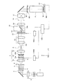
本発明の実施形態を、添付図面に基づいて説明する。図1は、本発明の実施形態にかかる露光装置の構成を概略的に示す図である。図1において、感光性基板であるウェハWの法線方向に沿ってZ軸を、ウェハWの面内において図1の紙面に平行な方向にY軸を、ウェハWの面内において図1の紙面に垂直な方向にX軸をそれぞれ設定している。 Embodiments of the present invention will be described with reference to the accompanying drawings. FIG. 1 is a drawing schematically showing a configuration of an exposure apparatus according to an embodiment of the present invention. In FIG. 1, the Z axis along the normal direction of the wafer W, which is a photosensitive substrate, the Y axis in the direction parallel to the plane of FIG. 1 in the plane of the wafer W, and the plane of the wafer W in FIG. The X axis is set in the direction perpendicular to the paper surface.
図1を参照すると、本実施形態の露光装置は、露光光(照明光)を供給するための光源1を備えている。光源1として、たとえば193nmの波長の光を供給するArFエキシマレーザ光源や248nmの波長の光を供給するKrFエキシマレーザ光源などを用いることができる。光源1から射出された光は、整形光学系2により所要の断面形状の光束に拡大され、1/4波長板として機能する第1可変位相差部材3、1/2波長板として機能する第2可変位相差部材4、デポラライザ(非偏光化素子)5、輪帯照明用の回折光学素子6を介して、アフォーカルレンズ7に入射する。
Referring to FIG. 1, the exposure apparatus of this embodiment includes a
第1可変位相差部材3、第2可変位相差部材4およびデポラライザ5は後述するように偏光状態切換手段を構成しているが、その構成および作用については後述する。アフォーカルレンズ7は、前側レンズ群7aの前側焦点位置と回折光学素子6の位置とがほぼ一致し且つ後側レンズ群7bの後側焦点位置と図中破線で示す所定面8の位置とがほぼ一致するように設定されたアフォーカル系(無焦点光学系)である。一般に、回折光学素子は、基板に露光光(照明光)の波長程度のピッチを有する段差を形成することによって構成され、入射ビームを所望の角度に回折する作用を有する。
The first variable
具体的には、輪帯照明用の回折光学素子6は、矩形状の断面を有する平行光束が入射した場合に、そのファーフィールド(またはフラウンホーファー回折領域)に輪帯状の光強度分布を形成する機能を有する。したがって、光束変換素子としての回折光学素子6に入射したほぼ平行光束は、アフォーカルレンズ7の瞳面に輪帯状の光強度分布を形成した後、輪帯状の角度分布でアフォーカルレンズ7から射出される。アフォーカルレンズ7の前側レンズ群7aと後側レンズ群7bとの間の光路中においてその瞳面またはその近傍には、可変位相差ユニット9および円錐アキシコン系10が配置されている。可変位相差ユニット9および円錐アキシコン系10の構成および作用については後述する。
Specifically, the diffractive optical element 6 for annular illumination forms an annular light intensity distribution in the far field (or Fraunhofer diffraction region) when a parallel light beam having a rectangular cross section is incident. It has a function. Accordingly, the substantially parallel light beam incident on the diffractive optical element 6 as the light beam conversion element forms an annular light intensity distribution on the pupil plane of the
アフォーカルレンズ7を介した光束は、σ値(σ値=照明光学装置のマスク側開口数/投影光学系のマスク側開口数)可変用のズームレンズ11および可変旋光ユニット12を介して、マイクロフライアイレンズ(またはフライアイレンズ)13に入射する。可変旋光ユニット12の構成および作用については後述する。マイクロフライアイレンズ13は、縦横に且つ稠密に配列された多数の正屈折力を有する微小レンズからなる光学素子である。一般に、マイクロフライアイレンズは、たとえば平行平面板にエッチング処理を施して微小レンズ群を形成することによって構成される。
The light beam that has passed through the
ここで、マイクロフライアイレンズを構成する各微小レンズは、フライアイレンズを構成する各レンズエレメントよりも微小である。また、マイクロフライアイレンズは、互いに隔絶されたレンズエレメントからなるフライアイレンズとは異なり、多数の微小レンズ(微小屈折面)が互いに隔絶されることなく一体的に形成されている。しかしながら、正屈折力を有するレンズ要素が縦横に配置されている点でマイクロフライアイレンズはフライアイレンズと同じ波面分割型のオプティカルインテグレータである。 Here, each micro lens constituting the micro fly's eye lens is smaller than each lens element constituting the fly eye lens. Further, unlike a fly-eye lens composed of lens elements isolated from each other, a micro fly-eye lens is formed integrally with a large number of micro lenses (micro refractive surfaces) without being isolated from each other. However, the micro fly's eye lens is the same wavefront division type optical integrator as the fly eye lens in that lens elements having positive refractive power are arranged vertically and horizontally.
所定面8の位置はズームレンズ11の前側焦点位置の近傍に配置され、マイクロフライアイレンズ13の入射面はズームレンズ11の後側焦点位置の近傍に配置されている。換言すると、ズームレンズ11は、所定面8とマイクロフライアイレンズ13の入射面とを実質的にフーリエ変換の関係に配置し、ひいてはアフォーカルレンズ7の瞳面とマイクロフライアイレンズ13の入射面とを光学的にほぼ共役に配置している。可変旋光ユニット12は、マイクロフライアイレンズ13の直前に配置され、ひいてはアフォーカルレンズ7の瞳面と光学的にほぼ共役に配置されている。
The position of the
したがって、マイクロフライアイレンズ13の入射面上には、アフォーカルレンズ7の瞳面と同様に、たとえば光軸AXを中心とした輪帯状の照野が形成される。この輪帯状の照野の全体形状は、ズームレンズ11の焦点距離に依存して相似的に変化する。マイクロフライアイレンズ13を構成する各微小レンズは、マスクM上において形成すべき照野の形状(ひいてはウェハW上において形成すべき露光領域の形状)と相似な矩形状の断面を有する。
Accordingly, on the incident surface of the micro fly's
マイクロフライアイレンズ13に入射した光束は多数の微小レンズにより二次元的に分割され、その後側焦点面またはその近傍(ひいては照明瞳)には、入射光束によって形成される照野とほぼ同じ光強度分布を有する二次光源、すなわち光軸AXを中心とした輪帯状の実質的な面光源からなる二次光源が形成される。マイクロフライアイレンズ13の後側焦点面またはその近傍に形成された二次光源からの光束は、ビームスプリッター14aおよびコンデンサー光学系15を介した後、マスクブラインド16を重畳的に照明する。ビームスプリッター14aを内蔵する偏光モニター14の構成および作用については後述する。
The light beam incident on the micro fly's
こうして、照明視野絞りとしてのマスクブラインド16には、マイクロフライアイレンズ13を構成する各微小レンズの形状と焦点距離とに応じた矩形状の照野が形成される。マスクブラインド16の矩形状の開口部(光透過部)を介した光束は、結像光学系17の集光作用を受けた後、所定のパターンが形成されたマスクMを重畳的に照明する。すなわち、結像光学系17は、マスクブラインド16の矩形状開口部の像をマスクM上に形成することになる。
Thus, a rectangular illumination field corresponding to the shape and focal length of each microlens constituting the micro fly's
マスクステージMS上に保持されたマスクMのパターンを透過した光束は、投影光学系PLを介して、ウェハステージWS上に保持されたウェハ(感光性基板)W上にマスクパターンの像を形成する。こうして、投影光学系PLの光軸AXと直交する平面(XY平面)内においてウェハステージWSを二次元的に駆動制御しながら、ひいてはウェハWを二次元的に駆動制御しながら一括露光またはスキャン露光を行うことにより、ウェハWの各露光領域にはマスクMのパターンが順次露光される。 The light beam that has passed through the pattern of the mask M held on the mask stage MS forms an image of the mask pattern on the wafer (photosensitive substrate) W held on the wafer stage WS via the projection optical system PL. . In this way, batch exposure or scan exposure is performed while the wafer stage WS is two-dimensionally driven and controlled in a plane (XY plane) orthogonal to the optical axis AX of the projection optical system PL, and thus the wafer W is two-dimensionally driven and controlled. As a result, the pattern of the mask M is sequentially exposed in each exposure region of the wafer W.
なお、輪帯照明用の回折光学素子6に代えて、4極照明用の回折光学素子(不図示)を照明光路中に設定することによって、4極照明を行うことができる。4極照明用の回折光学素子は、矩形状の断面を有する平行光束が入射した場合に、そのファーフィールドに4極状の光強度分布を形成する機能を有する。したがって、4極照明用の回折光学素子を介した光束は、マイクロフライアイレンズ13の入射面に、たとえば光軸AXを中心とした4つの円形状の照野からなる4極状の照野を形成する。その結果、マイクロフライアイレンズ13の後側焦点面またはその近傍にも、その入射面に形成された照野と同じ4極状の二次光源が形成される。
Instead of the diffractive optical element 6 for annular illumination, quadrupole illumination can be performed by setting a diffractive optical element (not shown) for quadrupole illumination in the illumination optical path. The diffractive optical element for quadrupole illumination has a function of forming a quadrupole light intensity distribution in the far field when a parallel light beam having a rectangular cross section is incident. Therefore, the light beam that has passed through the diffractive optical element for quadrupole illumination has a quadrupole illumination field composed of, for example, four circular illumination fields centered on the optical axis AX on the incident surface of the micro fly's
また、輪帯照明用の回折光学素子6に代えて、円形照明用の回折光学素子(不図示)を照明光路中に設定することによって、通常の円形照明を行うことができる。円形照明用の回折光学素子は、矩形状の断面を有する平行光束が入射した場合に、ファーフィールドに円形状の光強度分布を形成する機能を有する。したがって、円形照明用の回折光学素子を介した光束は、マイクロフライアイレンズ13の入射面に、たとえば光軸AXを中心とした円形状の照野を形成する。その結果、マイクロフライアイレンズ13の後側焦点面またはその近傍にも、その入射面に形成された照野と同じ円形状の二次光源が形成される。
Moreover, instead of the diffractive optical element 6 for annular illumination, a normal circular illumination can be performed by setting a diffractive optical element (not shown) for circular illumination in the illumination optical path. The diffractive optical element for circular illumination has a function of forming a circular light intensity distribution in the far field when a parallel light beam having a rectangular cross section is incident. Therefore, the light beam that has passed through the diffractive optical element for circular illumination forms, for example, a circular illumination field around the optical axis AX on the incident surface of the micro fly's
さらに、輪帯照明用の回折光学素子6に代えて、他の複数極照明用の回折光学素子(不図示)を照明光路中に設定することによって、様々な複数極照明(2極照明、8極照明など)を行うことができる。同様に、輪帯照明用の回折光学素子6に代えて、適当な特性を有する回折光学素子(不図示)を照明光路中に設定することによって、様々な形態の変形照明を行うことができる。 Furthermore, by replacing the diffractive optical element 6 for annular illumination with another diffractive optical element (not shown) for multipole illumination in the illumination optical path, various multipole illuminations (bipolar illumination, 8 Polar lighting etc.). Similarly, various forms of modified illumination can be performed by setting a diffractive optical element (not shown) having appropriate characteristics in the illumination optical path instead of the diffractive optical element 6 for annular illumination.
円錐アキシコン系10は、光源側から順に、光源側に平面を向け且つマスク側に凹円錐状の屈折面を向けた第1プリズム部材10aと、マスク側に平面を向け且つ光源側に凸円錐状の屈折面を向けた第2プリズム部材10bとから構成されている。そして、第1プリズム部材10aの凹円錐状の屈折面と第2プリズム部材10bの凸円錐状の屈折面とは、互いに当接可能なように相補的に形成されている。また、第1プリズム部材10aおよび第2プリズム部材10bのうち少なくとも一方の部材が光軸AXに沿って移動可能に構成され、第1プリズム部材10aの凹円錐状の屈折面と第2プリズム部材10bの凸円錐状の屈折面との間隔が可変に構成されている。以下、輪帯状または4極状の二次光源に着目して、円錐アキシコン系10の作用およびズームレンズ11の作用を説明する。
The
ここで、第1プリズム部材10aの凹円錐状屈折面と第2プリズム部材10bの凸円錐状屈折面とが互いに当接している状態では、円錐アキシコン系10は平行平面板として機能し、形成される輪帯状または4極状の二次光源に及ぼす影響はない。しかしながら、第1プリズム部材10aの凹円錐状屈折面と第2プリズム部材10bの凸円錐状屈折面とを離間させると、輪帯状または4極状の二次光源の幅(輪帯状の二次光源の外径と内径との差の1/2;4極状の二次光源に外接する円の直径(外径)と内接する円の直径(内径)との差の1/2)を一定に保ちつつ、輪帯状または4極状の二次光源の外径(内径)が変化する。すなわち、輪帯状または4極状の二次光源の輪帯比(内径/外径)および大きさ(外径)が変化する。
Here, in a state where the concave conical refracting surface of the
ズームレンズ11は、輪帯状または4極状の二次光源の全体形状を相似的に拡大または縮小する機能を有する。たとえば、ズームレンズ11の焦点距離を最小値から所定の値へ拡大させることにより、輪帯状または4極状の二次光源の全体形状が相似的に拡大される。換言すると、ズームレンズ11の作用により、輪帯状または4極状の二次光源の輪帯比が変化することなく、その幅および大きさ(外径)がともに変化する。このように、円錐アキシコン系10およびズームレンズ11の作用により、輪帯状または4極状の二次光源の輪帯比と大きさ(外径)とを制御することができる。
The
偏光モニター14は、マイクロフライアイレンズ13とコンデンサー光学系15との間の光路中に配置されたビームスプリッター14aを備えており、このビームスプリッター14aへの入射光の偏光状態を検知する機能を有する。換言すれば、偏光モニター14の検知結果に基づいて、マスクM(ひいてはウェハW)への照明光が所望の偏光状態(非偏光状態を含む概念)になっているか否かが随時検出される。
The polarization monitor 14 includes a
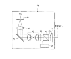
図2は、図1の偏光状態測定部の内部構成を概略的に示す図である。本実施形態では、図2に示すように、ウェハWを保持するためのウェハステージWSに、ウェハWに対する照明光(露光光)の偏光状態を測定するための偏光状態測定部18が設けられている。偏光状態測定部18は、ウェハWの露光面の高さ位置において二次元的に位置決め可能なピンホール部材40を備えている。なお、偏光状態測定部18の使用時には、ウェハWは光路から退避する。
FIG. 2 is a diagram schematically showing the internal configuration of the polarization state measurement unit of FIG. In the present embodiment, as shown in FIG. 2, a polarization
ピンホール部材40のピンホール40aを通過した光は、コリメートレンズ41を介してほぼ平行な光束になり、反射鏡42で反射された後、リレーレンズ系43に入射する。リレーレンズ系43を介したほぼ平行な光束は、移相子としてのλ/4板44および偏光子としての偏光ビームスプリッター45を介した後、二次元CCD46の検出面46aに達する。二次元CCD46の出力は、制御部(不図示)に供給される。ここで、λ/4板44は、光軸を中心として回転可能に構成されており、このλ/4板44には、その光軸を中心とした回転角を設定するための設定部47が接続されている。
The light that has passed through the pinhole 40 a of the
こうして、ウェハWに対する照明光の偏光度が0でない場合には、設定部47を介してλ/4板44を光軸廻りに回転させることにより二次元CCD46の検出面46aにおける光強度分布が変化する。したがって、偏光状態測定部18では、設定部47を用いてλ/4板44を光軸廻りに回転させながら検出面46aにおける光強度分布の変化を検出し、この検出結果から回転移相子法により照明光の偏光状態(偏光度;光に関するストークスパラメータS1,S2,S3)を測定することができる。Thus, when the polarization degree of the illumination light with respect to the wafer W is not 0, the light intensity distribution on the
なお、回転移相子法については、例えば鶴田著,「光の鉛筆−光技術者のための応用光学」,株式会社新技術コミュニケーションズなどに詳しく記載されている。実際には、ピンホール部材40(ひいてはピンホール40a)をウェハ面に沿って二次元的に移動させつつ、ウェハ面内の複数の位置における照明光の偏光状態を測定する。このとき、偏光状態測定部18では、二次元的な検出面46aにおける光強度分布の変化を検出するので、この検出分布情報に基づいて照明光の瞳内における偏光状態の分布を測定することができる。
The rotational phase shifter method is described in detail in, for example, Tsuruta, “Pencil of Light-Applied Optics for Optical Engineers”, New Technology Communications Inc. Actually, the polarization state of the illumination light at a plurality of positions in the wafer surface is measured while moving the pinhole member 40 (and thus the
ところで、偏光状態測定部18では、移相子としてλ/4板44に代えてλ/2板を用いることも可能である。どのような移相子を用いたとしても、光の偏光状態、すなわち光の4つのストークスパラメータを測定するためには、移相子と偏光子(偏光ビームスプリッター45)との光軸廻りの相対角度を変えたり、移相子または偏光子を光路から退避させたりして、少なくとも4つの異なる状態で検出面46aにおける光強度分布の変化を検出する必要がある。
By the way, in the polarization
なお、本実施形態では移相子としてのλ/4板44を光軸廻りに回転させたが、偏光子としての偏光ビームスプリッター45を光軸廻りに回転させても良く、移相子および偏光子の双方を光軸廻りに回転させても良い。また、この動作に代えて、あるいはこの動作に加えて、移相子としてのλ/4板44および偏光子としての偏光ビームスプリッター45のうちの一方または双方を光路から挿脱させても良い。
In this embodiment, the λ / 4
また、偏光状態測定部18では、反射鏡42の偏光特性により光の偏光状態が変化してしまう場合がある。この場合、反射鏡42の偏光特性は予めわかっているので、所要の計算によって反射鏡42の偏光特性の偏光状態への影響に基づいて偏光状態測定部18の測定結果を補正し、照明光の偏光状態を正確に測定することができる。また、反射鏡に限らず、レンズなどの他の光学部品に起因して偏光状態が変化してしまう場合でも同様に測定結果を補正し、照明光の偏光状態を正確に測定することができる。
In the polarization
こうして、偏光状態測定部18を用いてウェハWに対する照明光の瞳内における偏光状態(偏光度)を測定し、照明光が瞳内において適切な偏光状態になっているか否かが判定される。なお、上述の実施形態では、偏光状態測定部18がウェハステージWSに取り付け可能な構成を示したが、この偏光状態測定部18をウェハステージWSに組み込んでもよく、またウェハステージWSとは別のステージに組み込んでもよい。
Thus, the polarization state (degree of polarization) of the illumination light with respect to the wafer W in the pupil is measured using the polarization
図3は、本実施形態にかかる各可変位相差部材の構成を概略的に示す図である。本実施形態において、第1可変位相差部材3および第2可変位相差部材4は、図3(a)に示すソレイユ補償器として、あるいは図3(b)に示すバビネ補償器としてそれぞれ構成されている。図3(a)に示すソレイユ補償器は、光の入射側から順に、平行平面板21aと、一対の偏角プリズム21bおよび21cとにより構成されている。
FIG. 3 is a diagram schematically showing the configuration of each variable phase difference member according to the present embodiment. In the present embodiment, the first variable
ここで、平行平面板21a、第1偏角プリズム21bおよび第2偏角プリズム21cは、複屈折性を有する結晶材料としての水晶により形成されている。また、第1偏角プリズム21bと第2偏角プリズム21cとは、互いに補完的な(相補的な)くさび状の断面形状を有する。さらに、平行平面板21aの結晶光学軸と一対の偏角プリズム21bおよび21cの結晶光学軸とが互いに直交するように設定されている。
Here, the plane
また、たとえばマイクロメータヘッドのような駆動手段(不図示)により、第1偏角プリズム21bと第2偏角プリズム21cとがZ方向に沿って相対的に移動するように、あるいは第1偏角プリズム21bと第2偏角プリズム21cとが対向する斜面とYZ平面との交線方向に沿って相対的に移動するように構成されている。図3(a)に示すソレイユ補償器(21a〜21c)では、光の入射位置に依存することなく、第1偏角プリズム21bと第2偏角プリズム21cとの相対位置に応じて、入射光と射出光との間に一定の位相差が可変的に付与される。
Further, the first
一方、図3(b)に示すバビネ補償器は、光の入射側から順に、第1偏角プリズム22aと、第2偏角プリズム22bとにより構成されている。ここで、第1偏角プリズム22aおよび第2偏角プリズム22bは、複屈折性を有する結晶材料としての水晶により形成され、互いに補完的なくさび状の断面形状を有する。さらに、第1偏角プリズム22aの結晶光学軸と第2偏角プリズム22bの結晶光学軸とが互いに直交するように設定されている。
On the other hand, the Babinet compensator shown in FIG. 3B is composed of a
また、たとえばマイクロメータヘッドのような駆動手段(不図示)により、第1偏角プリズム22aと第2偏角プリズム22bとがZ方向に沿って相対的に移動するように、あるいは第1偏角プリズム22aと第2偏角プリズム22bとが対向する斜面とYZ平面との交線方向に沿って相対的に移動するように構成されている。図3(b)に示すバビネ補償器(22a,22b)では、Z方向に沿った光の入射位置にある程度依存するものの、第1偏角プリズム22aと第2偏角プリズム22bとの相対位置に応じて、入射光と射出光との間にほぼ一定の位相差が可変的に付与される。
Further, the first
本実施形態では、露光装置への搭載に先立って第1可変位相差部材3単体により入射光と射出光との間に付与される位相差を測定し、位相差が光の波長λの1/4になるように、すなわち第1可変位相差部材3が1/4波長板として正確に機能するように予め調整する。同様に、露光装置への搭載に先立って第2可変位相差部材4単体により入射光と射出光との間に付与される位相差を測定し、位相差が光の波長λの1/2になるように、すなわち第2可変位相差部材4が1/2波長板として正確に機能するように予め調整する。
In the present embodiment, prior to mounting on the exposure apparatus, the phase difference imparted between the incident light and the emitted light is measured by the first variable
次いで、1/4波長板として正確に機能するように調整された第1可変位相差部材3および1/2波長板として正確に機能するように調整された第2可変位相差部材4を、整形光学系2とデポラライザ5との間の光路中の所定位置にそれぞれ位置決めし、光軸AXを中心として一体的に回転できるようにそれぞれ設定する。こうして、1/4波長板としての第1可変位相差部材3は、光軸AXを中心として回転自在に構成されて、入射する楕円偏光の光を直線偏光の光に変換する。また、1/2波長板としての第2可変位相差部材4は、光軸AXを中心として回転自在に構成されて、入射する直線偏光の偏光方向を変化させる。
Next, the first variable
一方、デポラライザ5は、図示を省略したが、相補的な形状を有するくさび形状の水晶偏角プリズムとくさび形状の蛍石偏角プリズム(または石英偏角プリズム)とにより一体的なプリズム組立体として構成され、照明光路に対して挿脱自在に設定されている。なお、デポラライザ5の詳細な構成および作用については、たとえば国際公開第WO2004/051717号公報を参照することができる。
On the other hand, although not shown, the
光源1としてKrFエキシマレーザ光源やArFエキシマレーザ光源を用いる場合、これらの光源から射出される光は典型的には95%以上の偏光度を有し、第1可変位相差部材3にはほぼ直線偏光の光が入射する。しかしながら、光源1と第1可変位相差部材3との間の光路中に裏面反射鏡としての直角プリズムが介在する場合、入射する直線偏光の偏光面がP偏光面またはS偏光面に一致していないと、直角プリズムでの全反射により直線偏光が楕円偏光に変わる。
When a KrF excimer laser light source or an ArF excimer laser light source is used as the
偏光状態切換手段(3〜5)では、たとえば直角プリズムでの全反射に起因して楕円偏光の光が入射しても、入射する楕円偏光に対して1/4波長板としての第1可変位相差部材3を光軸AX廻りの所定の角度位置に設定することにより、楕円偏光の入射光が直線偏光の光に変換されて第2可変位相差部材4へ導かれる。また、入射する直線偏光に対して1/2波長板としての第2可変位相差部材4を光軸AX廻りの所要の角度位置に設定することにより、直線偏光の入射光が所望の方向に偏光方向を有する直線偏光の光に変換されてデポラライザ5へ、あるいは回折光学素子6へ直接導かれる。
In the polarization state switching means (3 to 5), for example, even if elliptically polarized light is incident due to total reflection by a right-angle prism, the first variable position as a quarter wavelength plate with respect to the incident elliptically polarized light. By setting the
また、デポラライザ5を照明光路中に挿入し、入射する直線偏光に対してデポラライザ5を光軸AX廻りの所定の角度位置に設定することにより、直線偏光の入射光が非偏光状態の光に変換(非偏光化)されて回折光学素子6に入射する。一方、デポラライザ5が照明光路から退避している場合、第2可変位相差部材4からの直線偏光の光は偏光方向を変えることなくそのまま回折光学素子6に入射する。
Further, by inserting the
こうして、偏光状態切換手段(3〜5)では、デポラライザ5を照明光路から退避させ、且つ1/4波長板としての第1可変位相差部材3および1/2波長板としての第2可変位相差部材4を光軸AX廻りの所定の角度位置にそれぞれ設定することにより、所望の方向に偏光方向を有する直線偏光の光を回折光学素子6に入射させることができる。また、1/4波長板としての第1可変位相差部材3および1/2波長板としての第2可変位相差部材4を光軸AX廻りの所定の角度位置にそれぞれ設定するとともに、デポラライザ5を照明光路中に挿入して光軸AX廻りの所定の角度位置に設定することにより、非偏光状態の光を回折光学素子6に入射させることができる。
Thus, in the polarization state switching means (3 to 5), the
換言すれば、偏光状態切換手段(3〜5)では、回折光学素子6への入射光の偏光状態(ひいてはマスクMおよびウェハWを照明する光の偏光状態)を直線偏光状態と非偏光状態との間で切り換えることができる。また、直線偏光状態の場合には、例えば互いに直交する偏光状態の間(Z方向偏光とX方向偏光との間)で切り換えることができる。 In other words, in the polarization state switching means (3 to 5), the polarization state of the light incident on the diffractive optical element 6 (and thus the polarization state of the light that illuminates the mask M and the wafer W) is changed between the linear polarization state and the non-polarization state. Can be switched between. In the case of a linear polarization state, for example, switching between orthogonal polarization states (between Z-direction polarization and X-direction polarization) can be performed.
以上のように、本実施形態では、1/4波長板や1/2波長板のような波長板を1枚の水晶板により製造する従来技術とは異なり、1/4波長板や1/2波長板のような波長板として機能する光学部材として、ソレイユ補償器やバビネ補償器のように入射光と射出光との間に位相差を可変的に付与する可変位相差部材(3,4)を用いている。したがって、可変位相差部材(3,4)を構成する光学要素(平行平面板や偏角プリズム)にある程度の製造誤差があっても、1/4波長板および1/2波長板として正確に機能するようにそれぞれ調整してから用いることができる。 As described above, in the present embodiment, unlike the prior art in which a wave plate such as a quarter wave plate or a half wave plate is manufactured using a single quartz plate, a quarter wave plate or a half wave plate is used. As an optical member that functions as a wave plate such as a wave plate, a variable phase difference member (3, 4) that variably gives a phase difference between incident light and outgoing light, such as a Soleil compensator and a Babinet compensator. Is used. Therefore, even if there are some manufacturing errors in the optical elements (parallel plane plates and declination prisms) constituting the variable phase difference members (3, 4), they function correctly as quarter-wave plates and half-wave plates. It can be used after being adjusted respectively.
したがって、本実施形態の照明光学装置(1〜17)では、波長板として機能する光学部材(3,4)を構成する各光学要素(21a〜21c;22a,22b)の製造誤差の影響を実質的に受けることなく、所望の偏光状態の光で被照射面としてのマスクMを照明することができる。その結果、本実施形態の露光装置(1〜WS)では、被照射面に設定されたマスクMを所望の偏光状態の光で照明する照明光学装置(1〜17)を用いて、適切な照明条件のもとで良好な露光を行うことができる。 Therefore, in the illumination optical device (1-17) of this embodiment, the influence of the manufacturing error of each optical element (21a-21c; 22a, 22b) which comprises the optical member (3, 4) which functions as a wavelength plate is substantial. The mask M as the irradiated surface can be illuminated with light having a desired polarization state without receiving light. As a result, in the exposure apparatus (1 to WS) of the present embodiment, appropriate illumination is performed using the illumination optical apparatus (1 to 17) that illuminates the mask M set on the irradiated surface with light having a desired polarization state. Good exposure can be performed under conditions.
なお、上述の説明では、可変位相差部材(3,4)単体による位相差を測定し、位相差が所定の値(光の波長λの1/4または1/2)になるように予め調整したものを照明光路中に組み込んでいる。しかしながら、これに限定されることなく、図4の第1変形例に示すように、可変位相差部材(3,4)を照明光路中に組み込んだ後に、偏光状態測定部18の測定結果に基づいて、可変位相差部材(3,4)が1/4波長板および1/2波長板として正確に機能するようにそれぞれ調整することもできる。また、1/4波長板および1/2波長板として正確に機能するように調整された状態から可変位相差部材(3,4)をさらに積極的にそれぞれ微調整することにより、多様な偏光状態の光で被照射面としてのマスクMを、ひいてはウェハWを照明することもできる。
In the above description, the phase difference due to the variable phase difference member (3, 4) alone is measured, and adjusted in advance so that the phase difference becomes a predetermined value (1/4 or 1/2 of the light wavelength λ). Is incorporated into the illumination light path. However, the present invention is not limited to this, and based on the measurement result of the polarization
図4において、制御部CRは、偏光状態測定部18からの測定結果を受け取り、可変位相差部材(3,4)中の光学要素(21a〜21c;22a,22b)間の相対位置を変更する駆動部DR3を制御し、被照射面としてのマスクMまたはウェハW上での偏光状態が所望の状態となるように、可変位相差部材(3,4)による位相差量を調整する。
In FIG. 4, the control unit CR receives the measurement result from the polarization
また、上述の説明では、可変位相差部材(3,4)を構成する各光学要素を水晶により形成しているが、これに限定されることなく、たとえばフッ化マグネシウムや方解石のような複屈折性の結晶材料を用いて可変位相差部材(3,4)の各光学要素を形成することもできる。 In the above description, each optical element constituting the variable phase difference member (3, 4) is formed of quartz, but is not limited to this, and birefringence such as magnesium fluoride or calcite is used. It is also possible to form each optical element of the variable phase difference member (3, 4) using a crystalline material.
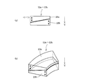
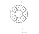
図5は、本実施形態にかかる可変旋光ユニットの構成を概略的に示す図である。また、図6は、図5の可変旋光ユニットを構成する各可変旋光部材の構成を概略的に示す図である。本実施形態にかかる可変旋光ユニット12は、マイクロフライアイレンズ13の直前に、すなわち照明光学系(2〜17)の瞳またはその近傍に配置されている。したがって、輪帯照明の場合、可変旋光ユニット12には光軸AXを中心としたほぼ輪帯状の断面を有する光束が入射することになる。
FIG. 5 is a diagram schematically showing the configuration of the variable optical rotation unit according to the present embodiment. FIG. 6 is a diagram schematically showing the configuration of each variable optical rotation member constituting the variable optical rotation unit of FIG. The variable
図5を参照すると、可変旋光ユニット12は、光軸AXを中心とする円の周方向に沿って配置された8つの可変旋光部材12a,12b,12c,12d,12e,12f,12gおよび12hにより構成されている。各可変旋光部材12a〜12hは、光軸AXを中心とした輪帯状の領域を円周方向に8等分して得られる扇形形状の外形を有し、且つ互いに同じ基本構成を有する。図6を参照すると、各可変旋光部材12a〜12hは、旋光性を有する光学材料としての水晶により形成された一対の偏角プリズム23aと23bとにより構成されている。
Referring to FIG. 5, the variable
第1偏角プリズム23aと第2偏角プリズム23bとは互いに補完的なくさび状の断面形状を有し、第1偏角プリズム23aの結晶光学軸および第2偏角プリズム23bの結晶光学軸がともに光軸AXに平行に(すなわちY方向に平行に)なるように配置されている。また、たとえばマイクロメータヘッドのような駆動手段(不図示)により、第1偏角プリズム23aと第2偏角プリズム23bとが光軸AXを中心とする円の径方向に沿って相対的に移動するように、あるいは第1偏角プリズム23aと第2偏角プリズム23bとが対向する斜面と光軸AXを含む平面との交線方向に沿って相対的に移動するように構成されている。
The
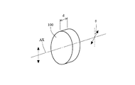
こうして、図6に示す各可変旋光部材12a〜12hでは、第1偏角プリズム23aと第2偏角プリズム23bとの相対位置に応じて、入射する直線偏光に旋光角度が可変的に付与される。以下、図7を参照して、水晶の旋光性について簡単に説明する。図7を参照すると、厚さdの水晶からなる平行平面板状の光学部材100が、その結晶光学軸と光軸AXとが一致するように配置されている。この場合、光学部材100の旋光性により、入射した直線偏光の偏光方向が光軸AX廻りにθだけ回転した状態で射出される。
Thus, in each of the variable
このとき、光学部材100の旋光性による偏光方向の回転角(旋光角度)θは、光学部材100の厚さdと水晶の旋光能ρとにより、次の式(a)で表わされる。
θ=d・ρ (a)At this time, the rotation angle (optical rotation angle) θ in the polarization direction due to the optical rotation of the
θ = d · ρ (a)
一般に、水晶の旋光能ρは、波長依存性(使用光の波長に依存して旋光能の値が異なる性質:旋光分散)があり、具体的には使用光の波長が短くなると大きくなる傾向がある。「応用光学II」の第167頁の記述によれば、250.3nmの波長を有する光に対する水晶の旋光能ρは、153.9度/mmである。 In general, the optical rotation ρ of quartz has a wavelength dependency (a property in which the value of optical rotation varies depending on the wavelength of the light used: optical rotation dispersion), and specifically, it tends to increase as the wavelength of the light used decreases. is there. According to the description on page 167 of “Applied Optics II”, the optical rotation power ρ of quartz with respect to light having a wavelength of 250.3 nm is 153.9 degrees / mm.
図8は、図5の可変旋光ユニットの作用により周方向偏光状態に設定された輪帯状の二次光源を概略的に示す図である。本実施形態において、光軸AXを挟んで対向する可変旋光部材12aおよび12eは、Z方向に偏光方向を有する直線偏光の光が入射した場合、Z方向をY軸廻りに+90度回転させた方向すなわちX方向に偏光方向を有する直線偏光の光を射出するように第1偏角プリズム23aと第2偏角プリズム23bとの相対位置が設定されている。したがって、この場合、図8に示す輪帯状の二次光源31のうち、可変旋光部材12aおよび12eの旋光作用を受けた光束が形成する一対の扇形領域(または円弧状領域)31aおよび31eを通過する光束の偏光方向はX方向になる。
FIG. 8 is a diagram schematically showing a ring-shaped secondary light source set in a circumferential polarization state by the action of the variable optical rotation unit of FIG. In this embodiment, the variable
光軸AXを挟んで対向する可変旋光部材12bおよび12fは、Z方向に偏光方向を有する直線偏光の光が入射した場合、Z方向をY軸廻りに+135度回転させた方向すなわちZ方向をY軸廻りに−45度回転させた方向に偏光方向を有する直線偏光の光を射出するように第1偏角プリズム23aと第2偏角プリズム23bとの相対位置が設定されている。したがって、この場合、図8に示す輪帯状の二次光源31のうち、可変旋光部材12bおよび12fの旋光作用を受けた光束が形成する一対の扇形領域31bおよび31fを通過する光束の偏光方向はZ方向をY軸廻りに−45度回転させた方向になる。
The variable
光軸AXを挟んで対向する可変旋光部材12cおよび12gは、Z方向に偏光方向を有する直線偏光の光が入射した場合、Z方向をY軸廻りに+180度回転させた方向すなわちZ方向に偏光方向を有する直線偏光の光を射出するように第1偏角プリズム23aと第2偏角プリズム23bとの相対位置が設定されている。したがって、この場合、図8に示す輪帯状の二次光源31のうち、可変旋光部材12cおよび12gの旋光作用を受けた光束が形成する一対の扇形領域31cおよび31gを通過する光束の偏光方向はZ方向になる。
The variable
光軸AXを挟んで対向する可変旋光部材12dおよび12hは、Z方向に偏光方向を有する直線偏光の光が入射した場合、Z方向をY軸廻りに+45度回転させた方向に偏光方向を有する直線偏光の光を射出するように第1偏角プリズム23aと第2偏角プリズム23bとの相対位置が設定されている。したがって、この場合、図8に示す輪帯状の二次光源31のうち、可変旋光部材12dおよび12hの旋光作用を受けた光束が形成する一対の扇形領域31dおよび31hを通過する光束の偏光方向はZ方向をY軸廻りに+45度回転させた方向になる。
The variable
このように、可変旋光ユニット12は、照明瞳面またはその近傍に配置されて入射光の偏光状態を所定の偏光状態に変換するための偏光変換素子を構成している。なお、本実施形態では、可変旋光ユニット12を光路から退避させることなく通常の円形照明を行うことができるように、可変旋光ユニット12の有効領域の径方向の大きさの3/10以上、好ましくは1/3以上の大きさを有し且つ旋光性を有しない円形状の中央領域12jが設けられている。ここで、中央領域12jは、たとえば石英や蛍石のように旋光性を有しない光学材料により形成されていてもよいし、単純に円形状の開口であってもよい。ただし、中央領域12jは可変旋光ユニット12に必須の要素ではない。
In this way, the variable
本実施形態では、周方向偏光輪帯照明(輪帯状の二次光源を通過する光束が周方向偏光状態に設定された変形照明)に際して、偏光状態切換手段(3〜5)の作用により、Z方向に偏光方向を有する直線偏光の光を可変旋光ユニット12に入射させる。その結果、マイクロフライアイレンズ13の後側焦点面またはその近傍には、図8に示すように、輪帯状の二次光源(輪帯状の照明瞳分布)31が形成され、この輪帯状の二次光源31を通過する光束が可変旋光ユニット12の作用により周方向偏光状態に設定される。周方向偏光状態では、輪帯状の二次光源31を構成する扇形領域31a〜31hをそれぞれ通過する光束は、各扇形領域31a〜31hの円周方向に沿った中心位置における光軸AXを中心とする円の接線方向とほぼ一致する偏光方向を有する直線偏光状態になる。
In the present embodiment, during the circumferential polarization annular illumination (deformed illumination in which the light beam passing through the annular secondary light source is set in the circumferential polarization state), the polarization state switching means (3-5) causes Z to Linearly polarized light having a polarization direction in the direction is incident on the variable
こうして、本実施形態では、可変旋光ユニット12の旋光作用により、光量損失を実質的に発生させることなく、周方向偏光状態の輪帯状の二次光源(照明瞳分布)31を形成することができる。なお、周方向偏光状態の輪帯状の照明瞳分布に基づく周方向偏光輪帯照明では、最終的な被照射面としてのウェハWに照射される光がS偏光を主成分とする偏光状態になる。ここで、S偏光とは、入射面に対して垂直な方向に偏光方向を有する直線偏光(入射面に垂直な方向に電気ベクトルが振動している偏光)のことである。ただし、入射面とは、光が媒質の境界面(被照射面:ウェハWの表面)に達したときに、その点での境界面の法線と光の入射方向とを含む面として定義される。
Thus, in the present embodiment, the annular secondary light source (illumination pupil distribution) 31 in the circumferentially polarized state can be formed by the optical rotation action of the variable
その結果、周方向偏光輪帯照明では、投影光学系PLの光学性能(焦点深度など)の向上を図ることができ、ウェハ(感光性基板)W上において高いコントラストのマスクパターン像を得ることができる。すなわち、本実施形態の露光装置では、光量損失を良好に抑えつつ周方向偏光状態の輪帯状の照明瞳分布を形成することのできる照明光学装置を用いているので、適切な照明条件のもとで微細パターンを忠実に且つ高スループットで転写することができる。 As a result, in the circumferential polarization annular illumination, the optical performance (such as the depth of focus) of the projection optical system PL can be improved, and a high-contrast mask pattern image can be obtained on the wafer (photosensitive substrate) W. it can. That is, in the exposure apparatus of the present embodiment, an illumination optical apparatus that can form a ring-shaped illumination pupil distribution in a circumferentially polarized state while suppressing light amount loss satisfactorily is used. Thus, a fine pattern can be transferred faithfully and with high throughput.
また、本実施形態では、偏光状態切換手段(3〜5)の作用によりX方向に偏光方向を有する直線偏光の光を可変旋光ユニット12に入射させて、図9に示すように輪帯状の二次光源32を通過する光束を径方向偏光状態に設定し、径方向偏光輪帯照明(輪帯状の二次光源32を通過する光束が径方向偏光状態に設定された変形照明)を行うことができる。径方向偏光状態では、輪帯状の二次光源32を構成する扇形領域32a〜32hをそれぞれ通過する光束は、扇形領域32a〜32hの円周方向に沿った中心位置における光軸AXを中心とする円の半径方法とほぼ一致する偏光方向を有する直線偏光状態になる。
Further, in the present embodiment, linearly polarized light having a polarization direction in the X direction is made incident on the variable
径方向偏光状態の輪帯状の照明瞳分布に基づく径方向偏光輪帯照明では、最終的な被照射面としてのウェハWに照射される光がP偏光を主成分とする偏光状態になる。ここで、P偏光とは、上述のように定義される入射面に対して平行な方向に偏光方向を有する直線偏光(入射面に平行な方向に電気ベクトルが振動している偏光)のことである。その結果、径方向偏光輪帯照明では、ウェハWに塗布されたレジストにおける光の反射率を小さく抑えて、ウェハ(感光性基板)W上において良好なマスクパターン像を得ることができる。 In the radial polarization annular illumination based on the annular illumination pupil distribution in the radial polarization state, the light irradiated on the wafer W as the final irradiated surface is in a polarization state mainly composed of P-polarized light. Here, the P-polarized light is linearly polarized light having a polarization direction in a direction parallel to the incident surface defined as described above (polarized light whose electric vector is oscillating in a direction parallel to the incident surface). is there. As a result, in the radial polarization annular illumination, it is possible to obtain a good mask pattern image on the wafer (photosensitive substrate) W while suppressing the reflectance of light in the resist applied to the wafer W to be small.
ところで、本出願人は、たとえば国際公開第WO2005/076045号パンフレットにおいて、照明瞳面またはその近傍に配置されて入射光の偏光状態を所定の偏光状態に変換するための偏光変換素子として、光の透過方向に沿った厚さ(光軸方向の長さ)が互いに異なる複数種類の水晶板を旋光部材として円周方向に配置する構成を提案している。上記出願において提案された偏光変換素子では、入射する直線偏光に所要の旋光角度を付与するための各旋光部材を1枚の水晶板で精度良く製造することは困難である。製造誤差に起因して各旋光部材が正確に機能しない場合には、所望の周方向偏光状態や径方向偏光状態などを実現することができない。 By the way, the present applicant, for example, in International Publication No. WO2005 / 076045 pamphlet, as a polarization conversion element that is arranged on or near the illumination pupil plane and converts the polarization state of incident light into a predetermined polarization state, A configuration is proposed in which a plurality of types of quartz plates having different thicknesses in the transmission direction (length in the optical axis direction) are arranged in the circumferential direction as optical rotation members. In the polarization conversion element proposed in the above-mentioned application, it is difficult to accurately manufacture each optical rotation member for giving a required optical rotation angle to incident linearly polarized light with one crystal plate. If each optical rotatory member does not function correctly due to a manufacturing error, a desired circumferential polarization state, radial polarization state, or the like cannot be realized.
これに対し、本実施形態では、偏光変換素子としての可変旋光ユニット12を、第1偏角プリズム23aと第2偏角プリズム23bとの相対位置に応じて入射する直線偏光に旋光角度を可変的に付与する複数の可変旋光部材12a〜12hにより構成している。したがって、各可変旋光部材12a〜12hを構成する光学要素(一対の偏角プリズム)にある程度の製造誤差があっても、所要の旋光角度を付与する光学部材として正確に機能するように各可変旋光部材12a〜12hをそれぞれ調整してから可変旋光ユニット12を用いることができる。
On the other hand, in the present embodiment, the variable
具体的には、露光装置への搭載に先立って各可変旋光部材12a〜12hによる旋光角度をそれぞれ測定し、旋光角度が所定の値になるように各可変旋光部材12a〜12hを(ひいては第1偏角プリズム23aと第2偏角プリズム23bとの相対位置)を調整してから、可変旋光ユニット12を照明光路中に組み込む。あるいは、可変旋光ユニット12を照明光路中に組み込んだ後に、偏光状態測定部18の測定結果に基づいて、各可変旋光部材12a〜12hが正確に機能するように第1偏角プリズム23aと第2偏角プリズム23bとの相対位置をそれぞれ調整することもできる。また、可変旋光ユニット12として正確に機能するように調整された状態から各可変旋光部材12a〜12hをさらに積極的にそれぞれ微調整することにより、多様な偏光状態(たとえば完全な周方向偏光状態と僅かに異なる変形周方向偏光状態など)の光で被照射面としてのマスクMを、ひいてはウェハWを照明することもできる。
Specifically, prior to mounting in the exposure apparatus, the optical rotation angles by the variable
この場合、図1に示すように、制御部CRは、偏光状態測定部18からの測定結果を受け取り、可変旋光ユニット12中の光学要素(12a〜12h)の相対位置を変更する駆動部DR1を制御し、被照射面としてのマスクMまたはウェハW上に向かう光束の偏光状態が所望の状態となるように、可変旋光ユニット12による旋光量の分布を調整する。
In this case, as shown in FIG. 1, the control unit CR receives the measurement result from the polarization
こうして、本実施形態の照明光学装置(1〜17)では、可変旋光ユニット12を構成する各光学要素(12a〜12h;23a,23b)の製造誤差の影響を実質的に受けることなく、所望の偏光状態の光で被照射面としてのマスクMを照明することができる。その結果、本実施形態の露光装置(1〜WS)では、被照射面に設定されたマスクMを所望の偏光状態の光で照明する照明光学装置(1〜17)を用いて、適切な照明条件のもとで良好な露光を行うことができる。
Thus, in the illumination optical device (1-17) of the present embodiment, a desired optical device (12a-12h; 23a, 23b) constituting the variable
なお、上述の説明では、可変旋光ユニット12に入射する光束を、Z方向に偏光方向を有する直線偏光状態とX方向に偏光方向を有する直線偏光状態との間で切り換えることにより、周方向偏光輪帯照明と径方向偏光輪帯照明とを実現している。しかしながら、これに限定されることなく、たとえばZ方向またはX方向に偏光方向を有する直線偏光状態の入射光束に対して、可変旋光ユニット12を図5に示す第1状態と光軸AX廻りに90度だけ回転させた第2状態との間で切り換えることにより、周方向偏光輪帯照明と径方向偏光輪帯照明とを実現することもできる。
In the above description, the circumferential polarization ring is switched by switching the light beam incident on the variable
また、上述の説明では、マイクロフライアイレンズ13の直前に可変旋光ユニット12を配置している。しかしながら、これに限定されることなく、一般に照明光学装置(1〜PL)の瞳またはその近傍に、たとえば投影光学系PLの瞳またはその近傍や、結像光学系17の瞳またはその近傍や、円錐アキシコン系10の直前(アフォーカルレンズ7の瞳またはその近傍)などに可変旋光ユニット12を配置することもできる。
In the above description, the variable
また、上述の説明では、輪帯状の有効領域の8分割に対応する8つの扇形形状の可変旋光部材12a〜12hにより可変旋光ユニット12を構成している。しかしながら、これに限定されることなく、たとえば円形状の有効領域の8分割に対応する8つの扇形形状の可変旋光部材により、あるいは円形状または輪帯状の有効領域の4分割に対応する4つの扇形形状の可変旋光部材により、あるいは円形状または輪帯状の有効領域の16分割に対応する16つの扇形形状の可変旋光部材により可変旋光ユニット12を構成することもできる。すなわち、可変旋光ユニット12の有効領域の形状、有効領域の分割数(可変旋光部材の数)などについて様々な変形例が可能である。
In the above description, the variable
また、上述の説明では、水晶を用いて各可変旋光部材12a〜12hを(ひいては可変旋光ユニット12を)形成している。しかしながら、これに限定されることなく、旋光性を有する他の適当な光学材料を用いて各可変旋光部材を形成することもできる。この場合、使用波長の光に対して100度/mm以上の旋光能を有する光学材料を用いることが好ましい。すなわち、旋光能の小さい光学材料を用いると、偏光方向の所要回転角を得るために必要な厚さが大きくなり過ぎて、光量損失の原因になるので好ましくない。
In the above description, each of the variable
また、上述の説明において、可変旋光ユニット12を照明光路に対して固定的に設けたが、この可変旋光ユニット12を照明光路に対して挿脱可能に設けても良い。また、上述の説明では、ウェハWに対するS偏光と輪帯照明とを組み合わせた例を示したが、ウェハWに対するS偏光と2極や4極や8極などの多極照明および円形照明とを組み合わせても良い。
In the above description, the variable
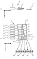
図10は、本実施形態にかかる可変位相差ユニットの構成を概略的に示す図である。本実施形態にかかる可変位相差ユニット9は、アフォーカルレンズ7の瞳面またはその近傍に、すなわち照明光学系(2〜17)の瞳またはその近傍に配置されている。したがって、輪帯照明の場合、可変位相差ユニット9には、光軸AXを中心としたほぼ輪帯状の断面を有する光束が入射することになる。また、8極照明の場合、可変位相差ユニット9には、例えば光軸AXを中心とした8つのほぼ円形状の断面を有する光束が入射することになる。以下、説明を単純化するために8極照明の場合について説明する。
FIG. 10 is a diagram schematically showing the configuration of the variable phase difference unit according to the present embodiment. The variable
図10を参照すると、可変位相差ユニット9は、光軸AXを中心とする円の周方向に沿って配置された8つの円形状の可変位相差部材9a,9b,9c,9d,9e,9f,9gおよび9hにより構成されている。各可変位相差部材9a〜9hは、互いに同じ基本構成を有し、具体的には図3(a)に示すソレイユ補償器として、あるいは図3(b)に示すバビネ補償器としてそれぞれ構成されている。
Referring to FIG. 10, the variable
また、各可変位相差部材9a〜9hは、たとえば円形状の外形の中心を通り光軸AXに平行な(Y方向に平行な)軸線を中心として回転自在に構成されている。一例として上述の周方向偏光状態で8極照明を行う場合、図11に示すように、偏光状態切換手段(3〜5)の作用により、可変位相差ユニット9に入射する8極状の光束33を構成する8つの円形状の光束33a〜33hはすべてZ方向に偏光方向を有する直線偏光であるはずである。
Each of the variable
しかしながら、第2可変位相差部材4と可変位相差ユニット9との間の光路中に配置された光学部材の偏光特性などの影響により、可変位相差ユニット9に達する光束の偏光状態がZ方向に偏光方向を有する直線偏光状態から変化することがある。単純な具体例として、図11に示すように、たとえば可変位相差ユニット9の可変位相差部材9aに入射する円形状の光束33aが楕円偏光状態になったり、可変位相差部材9hに入射する円形状の光束33hがZ方向に対して傾いた方向に偏光方向を有する直線偏光状態になったりする。
However, due to the influence of the polarization characteristics of the optical member disposed in the optical path between the second variable
この場合、本実施形態の可変位相差ユニット9では、可変位相差部材9aが1/4波長板として正確に機能するように、第1偏角プリズム21bと第2偏角プリズム21cとの相対位置(あるいは第1偏角プリズム22aと第2偏角プリズム22bとの相対位置)を調整する。また、可変位相差部材9hが1/2波長板として正確に機能するように、第1偏角プリズム21bと第2偏角プリズム21cとの相対位置(あるいは第1偏角プリズム22aと第2偏角プリズム22bとの相対位置)を調整する。
In this case, in the variable
次いで、可変位相差部材9aを中心軸線廻りの所定の角度位置に設定することにより、楕円偏光の入射光をZ方向に偏光方向を有する直線偏光の光に変換する。また、可変位相差部材9hを中心軸線廻りの所定の角度位置に設定することにより、直線偏光の入射光をZ方向に偏光方向を有する直線偏光の光に変換する。こうして、照明瞳面またはその近傍に配置された偏光変換素子としての可変位相差ユニット9の作用により、入射光の偏光状態を所望の偏光状態(具体例ではZ方向に偏光方向を有する直線偏光状態)に変換することができ、ひいては所望の偏光状態(たとえば周方向偏光状態、径方向偏光状態、Z方向に偏光方向を有する直線偏光状態など)でマスクMおよびウェハWを照明することができる。すなわち、本実施形態にかかる可変位相差ユニット9を用いて、照明瞳面もしくはその近傍の位置での偏光状態を局所的に変更することにより、照明瞳面もしくはその近傍において所望の偏光状態の分布を持つ照明光でマスクMおよびウェハWを照明することができ、ひいては所望の解像度や焦点深度向上の効果が得られるだけでなく、たとえばパターン左右方向や上下方向における非対称誤差の発生を抑えることができる。
Next, by setting the variable
なお、上述の説明では、8極照明を行う場合に着目しているが、これに限定されることなく、たとえば2極、4極のような複数極照明や、輪帯照明を行う場合にも同様に、偏光変換素子としての可変位相差ユニット9の作用により入射光の偏光状態を所望の偏光状態に変換することができる。また、上述の説明では、可変位相差ユニット9をアフォーカルレンズ7の瞳面またはその近傍に配置しているが、これに限定されることなく、一般的に照明光学系(2〜17)の瞳面またはその近傍に配置することもできる。ちなみに、可変位相差ユニット9を照明光路に対して挿脱自在に設けてもよいし、照明光路中に固定的に設けてもよい。
In the above description, attention is paid to the case of performing 8-pole illumination, but the present invention is not limited to this. For example, multi-pole illumination such as 2-pole and 4-pole or annular illumination is also performed. Similarly, the polarization state of incident light can be converted into a desired polarization state by the action of the variable
また、上述の説明では、可変位相差ユニット9を通過した直後の8極状の光束33a〜33hがすべてZ方向に偏光方向を有する直線偏光状態になるように調整しているが、これに限定されることなく、可変位相差ユニット9を通過した直後の光束が様々な偏光状態になるように調整することもできる。
In the above description, the octupole
また、偏光状態測定部18の測定結果に基づいて、ある調整状態から各可変位相差部材9a〜9hをさらに積極的にそれぞれ微調整することにより、さらに多様な偏光状態の光で被照射面としてのマスクMを、ひいてはウェハWを照明することもできる。この場合、制御部CRは、図1に示した駆動部DR2を介して可変位相差ユニット9中の各可変位相差部材9a〜9hを調整する。
Further, based on the measurement result of the polarization
なお、図5に示した可変旋光ユニット12と図10に示した可変位相差ユニット9とを組み合わせて用いても良い。この場合、可変位相差ユニット9によって照明光の楕円偏光率を制御し、可変旋光ユニット12によって偏光方向(楕円偏光の場合はその長軸方向)を制御することが好ましい。このとき、可変位相差ユニット9と可変旋光ユニット12とを隣接した状態で配置しても良いし、これらのユニット間にリレー光学系(7b,11)を挟んで、これらのユニット9と12とが互いに共役になるように配置しても良い。
Note that the variable
図12は、本実施形態にかかる別の可変位相差ユニットの構成を概略的に示す図である。図12に示す可変位相差ユニット19は、図12(a)に示すように、マスクブラインド16の近傍に、すなわち照明光学装置(1〜17)の被照射面と光学的に共役な位置またはその近傍に配置されている。したがって、可変位相差ユニット19には、輪帯照明や複数極照明や円形照明などに依存することなく、マスクM上の照明領域やウェハW上の露光領域(スキャン露光の場合には静止露光領域)とほぼ相似な矩形状の光束が入射することになる。
FIG. 12 is a diagram schematically showing the configuration of another variable phase difference unit according to this embodiment. As shown in FIG. 12A, the variable
図12(b)を参照すると、可変位相差ユニット19は、光軸AXを中心とする矩形状の領域内にほぼ稠密配置された多数の円形状の可変位相差部材19a,19b,19c,19d,19e,・・・により構成されている。各可変位相差部材(19a〜19e,・・・)は、互いに同じ基本構成を有し、具体的には図3(a)に示すソレイユ補償器として、あるいは図3(b)に示すバビネ補償器としてそれぞれ構成されている。
Referring to FIG. 12B, the variable
また、各可変位相差部材(19a〜19e,・・・)は、たとえば円形状の外形の中心を通り光軸AXに平行な(Y方向に平行な)軸線を中心として回転自在に構成されている。一例としてY方向に偏光方向を有する直線偏光状態でマスクMおよびウェハWを照明する場合、図13に示すように、偏光状態切換手段(3〜5)の作用により、可変位相差ユニット19の各可変位相差部材(19a〜19e,・・・)に入射する光束はすべてZ方向に偏光方向を有する直線偏光であるはずである。
Each of the variable phase difference members (19a to 19e,...) Is configured to be rotatable about an axis passing through the center of a circular outer shape and parallel to the optical axis AX (parallel to the Y direction), for example. Yes. As an example, when illuminating the mask M and the wafer W in a linear polarization state having a polarization direction in the Y direction, as shown in FIG. 13, each of the variable
しかしながら、第2可変位相差部材4と可変位相差ユニット19との間の光路中に配置された光学部材の偏光特性などの影響により、可変位相差ユニット19に達する光束の偏光状態がZ方向に偏光方向を有する直線偏光状態から変化することがある。単純な具体例として、図13に示すように、たとえば可変位相差ユニット19の可変位相差部材19aに入射する光束が楕円偏光状態になったり、可変位相差部材19eに入射する光束がZ方向に対して傾いた方向に偏光方向を有する直線偏光状態になったりする。
However, the polarization state of the light beam reaching the variable
この場合、図12の可変位相差ユニット19では、可変位相差部材19aが1/4波長板として正確に機能するように、第1偏角プリズム21bと第2偏角プリズム21cとの相対位置(あるいは第1偏角プリズム22aと第2偏角プリズム22bとの相対位置)を調整する。また、可変位相差部材19eが1/2波長板として正確に機能するように、第1偏角プリズム21bと第2偏角プリズム21cとの相対位置(あるいは第1偏角プリズム22aと第2偏角プリズム22bとの相対位置)を調整する。
In this case, in the variable
次いで、可変位相差部材19aを中心軸線廻りの所定の角度位置に設定することにより、楕円偏光の入射光をZ方向に偏光方向を有する直線偏光の光に変換する。また、可変位相差部材19eを中心軸線廻りの所定の角度位置に設定することにより、直線偏光の入射光をZ方向に偏光方向を有する直線偏光の光に変換する。こうして、被照射面と光学的に共役な位置またはその近傍に配置された偏光変換素子としての可変位相差ユニット19の作用により、入射光の偏光状態を所望の偏光状態(具体例ではZ方向に偏光方向を有する直線偏光状態)に変換することができ、ひいては所望の偏光状態(Y方向に偏光方向を有する直線偏光状態)でマスクMおよびウェハWを照明することができる。すなわち、本実施形態にかかる別の可変位相差ユニット19を用いて、被照射面(マスクM,ウェハW)を照明する光の偏光状態を局所的に変更することにより、被照射面上において所望の偏光状態の分布を持つ照明光でマスクMおよびウェハWを照明することができ、ひいてはウェハW上に形成されるパターンの線幅が露光領域内の位置毎にばらつくのを抑え、いわゆるフィールド内線幅差の発生を抑えることができる。
Next, by setting the variable
なお、図5の可変旋光ユニットと図12の可変位相差ユニット、あるいは図10の可変位相差ユニットと図12の可変位相差ユニットとを併用することもできる。この場合、照明瞳面もしくはその近傍での偏光状態を局所的に連続変更しつつ被照射面(マスクM,ウェハW)を照明する光の偏光状態を局所的に連続変更することにより、照明瞳面もしくはその近傍において所望の偏光状態の分布を持ち且つ被照射面上において所望の偏光状態の分布を持つ照明光でマスクMおよびウェハWを照明することができ、ひいてはパターンの非対称誤差の発生およびフィールド内線幅差の発生などを抑えることができる。 5 and the variable phase difference unit of FIG. 12, or the variable phase difference unit of FIG. 10 and the variable phase difference unit of FIG. 12 can be used in combination. In this case, by changing the polarization state of the light that illuminates the irradiated surface (mask M, wafer W) locally and continuously while locally changing the polarization state at or near the illumination pupil surface, the illumination pupil is changed. The mask M and the wafer W can be illuminated with illumination light having a desired polarization state distribution at or near the surface and having a desired polarization state distribution on the surface to be irradiated. Generation of line width differences in the field can be suppressed.
なお、上述の説明では、可変位相差ユニット19をマスクブラインド16の近傍に配置している。しかしながら、これに限定されることなく、マスクブラインド16の近傍以外に、照明光学装置(1〜17)の被照射面の近傍(たとえばマスクMの近傍)、被照射面と光学的に共役な位置、または該共役な位置の近傍に配置することもできる。ちなみに、可変位相差ユニット19を照明光路に対して挿脱自在に設けてもよいし、照明光路中に固定的に設けてもよい。また、スキャン露光の場合には、多数の円形状の可変位相差部材を非スキャン方向に沿って配置することが好ましく、また非スキャン方向に沿った配置が千鳥状(あるいはジグザグ状)となることが好ましい。
In the above description, the variable
また、上述の説明では、可変位相差ユニット19を通過した直後の光束がすべてZ方向に偏光方向を有する直線偏光状態になるように調整しているが、これに限定されることなく、可変位相差ユニット19を通過した直後の光束が様々な偏光状態になるように調整することもできる。また、偏光状態測定部18の測定結果に基づいて、ある調整状態から各可変位相差部材(19a〜19e,・・・)をさらに積極的にそれぞれ微調整することにより、多様な偏光状態の光で被照射面としてのマスクMを、ひいてはウェハWを照明することもできる。
In the above description, the light beams immediately after passing through the variable
この場合、図12に示すように、制御部CRは、偏光状態測定部18からの測定結果を受け取り、可変位相差ユニット19中の可変位相差部材19a〜19eを駆動する駆動部DR4を制御し、被照射面としてのマスクMまたはウェハW上での光束の偏光状態分布が所望の状態となるように、可変位相差ユニット19による位相差量の分布を調整する。
In this case, as shown in FIG. 12, the control unit CR receives the measurement result from the polarization
また、上述の実施形態では、照明光学装置(1〜17)の被照射面と光学的に共役な位置またはその近傍に可変位相差ユニット19を配置しているが、この可変位相差ユニットに代えて、複数の可変旋光ユニットを配置しても良い。この場合、それぞれの可変旋光部材の形状は、図5に示したような扇形状ではなく、円形状であることが好ましい。この構成により、被照射面上において所望の偏光方向の分布を持つ照明光で直線偏光照明を行うことができる。ひいては、被照射面上において所望の偏光状態の分布を持つ照明光で偏光照明を行うことができる。なお、このような可変旋光ユニットと可変位相差ユニットとを組み合わせて用いても良い。この場合、可変位相差ユニットによって照明光の楕円偏光率を制御し、可変旋光ユニットによって偏光方向(楕円偏光の場合はその長軸方向)を制御することが好ましい。
In the above-described embodiment, the variable
また、図14に第2変形例として示すように、可変旋光ユニット80として、非スキャン方向(X方向)に対応した方向に沿って、クサビ状に形成された旋光性を有する光学材料(たとえば水晶)からなる可変旋光部材81a〜81fを配置しても良い。これらの可変旋光部材81a〜81fはスキャン方向に対応する方向(Z方向)に可動であり、その移動量は、制御部CRにより制御されて各可変旋光部材81a〜81fに接続された駆動ユニット82a〜82fにより調整される。
Further, as shown in FIG. 14 as a second modified example, as the variable
図14(b)を参照して、各可変旋光部材81a〜81fの作用について説明する。なお、ここでは可変旋光部材81fを代表として説明する。図14(b)において、可変旋光部材81fの移動方向(Z方向)に沿った複数の位置83f1〜83f5を考える。このとき、マスクブラインド16の開口部16a内の複数の位置83f1〜83f5を通過した各光束の偏光状態を84f1〜84f5で示す。可変旋光部材81fを介さない光束の偏光状態84f1〜84f3に対して、可変旋光部材81fを介した光束の偏光状態84f4,84f5は、可変旋光部材81fの光軸方向(Y方向)の厚みに応じて、入射した直線偏光の偏光方向が光軸廻りに回転する。
With reference to FIG.14 (b), the effect | action of each variable
ここで、スキャン露光を考えると、ウェハW上の一点に達する光束の偏光状態は、スキャン方向に沿った光束群の平均的な偏光状態と考えることができる。第2変形例では、可変旋光部材81fのZ方向位置に応じて、Z方向に沿った光束の偏光状態84f1〜84f5の平均的な偏光状態を変更できるため、ウェハW上の一点に達する光束の偏光状態を変更することができる。そして、非スキャン方向に沿った各可変旋光部材81a〜81fのZ方向位置をそれぞれ変更することにより、非スキャン方向での光束の偏光状態の分布を変更できる。なお、図15に示すように、可変旋光ユニットの各可変旋光部材81a〜81fに、光軸補正用の非晶質材料(たとえば石英)からなるクサビ状の光学部材85a〜85f(図15では85fのみ図示)を設け、全体として平行平面板状にしても良い。
Here, considering scan exposure, the polarization state of the light beam reaching one point on the wafer W can be considered as the average polarization state of the light beam group along the scan direction. In the second modified example, the average polarization state of the polarization states 84f1 to 84f5 of the light beam along the Z direction can be changed according to the position of the variable
図16は、第3変形例にかかる可変旋光/移相ユニットの構成を概略的に示す図である。第3変形例は、可変旋光子を用いて直線偏光の偏光方向(楕円偏光の長軸方向の向き)を制御しつつ、可変移相子を用いて偏光の楕円率を制御するものである。図16(a)に示す側面図、図16(b)に示す上面図および図16(c)に示す下面図を参照すると、旋光子51〜55はそれぞれ結晶光学軸が光軸方向を向いた水晶から形成されており、移相子61〜66はそれぞれ結晶光学軸が光軸直交方向を向いた水晶から形成されている。
FIG. 16 is a diagram schematically showing a configuration of a variable optical rotation / phase shifting unit according to a third modification. The third modification is to control the ellipticity of polarized light using a variable phase shifter while controlling the polarization direction of linearly polarized light (direction of the major axis direction of elliptically polarized light) using a variable optical rotator. Referring to the side view shown in FIG. 16 (a), the top view shown in FIG. 16 (b), and the bottom view shown in FIG. 16 (c), each of the
ここで、旋光子51および移相子61は四角錐形状をなしており、旋光子52〜55ならびに移相子62〜65はそれぞれ(光軸を含む面内での)断面がくさび形状で光軸方向から見て四分円形状をなしている。また、移相子61〜65における旋光作用をキャンセルするため、移相子61〜65の結晶光学軸方向と移相子66の結晶光学軸方向とは互いに直交している。また、旋光子52〜55は、旋光子51に対して光軸を基準とする半径方向に可動に設けられており、移相子62〜65は、移相子61に対して光軸を基準とする半径方向に可動に設けられている。このとき、旋光子52〜55は、四角錐形状の旋光子51の斜面に沿って可動であることが好ましく、移相子62〜65は、四角錐形状の移相子61の斜面に沿って可動であることが好ましい。
Here, the
旋光子52〜55の半径方向の位置に応じて、旋光子全体としての光軸方向の厚みが局所的に変更される。また、移相子62〜65の半径方向の位置に応じて移相子全体としての光軸方向の厚みが局所的に変更される。従って、旋光子51,52および移相子61,62,66を通過する第1の光束、旋光子51,53および移相子61,63,66を通過する第2の光束、旋光子51,54および移相子61,64,66を通過する第3の光束、および旋光子51,55および移相子61,65,66を通過する第4の光束のそれぞれに与える旋光量および移相量を独立に調整することができるため、第1〜第4の光束のそれぞれの偏光状態(偏光方向および楕円率)を独立調整することができる。
Depending on the radial positions of the
なお、移相量を効果的に調整(補正)するためには、本変形例のように可変移相ユニット(61〜66)の入射側に可変旋光ユニット(51〜55)を配置することが望ましい。ここで、可変移相ユニット(61〜66)の射出側に可変旋光ユニット(51〜55)が配置される場合には、可変移相ユニット(51〜55)の移相子の結晶軸方位と移相子51〜55に入射する光の偏光方向とが平行または垂直となる可能性があり、このときには入射光に対して移相作用を与えることができない。この場合には、可変位相ユニット(51〜55)の移相子51〜55の結晶軸を光軸直交面内で任意の方向に回転させるための移相子回転機構を設けるか、異なる方位の結晶軸を持つ移相子と交換可能に設けることが好ましい。このように、光の入射側から可変旋光ユニットおよび可変移相ユニットの順に配置することは、本変形例だけではなく後述の変形例および実施形態においても有効である。
In order to effectively adjust (correct) the amount of phase shift, the variable optical rotation units (51 to 55) may be arranged on the incident side of the variable phase shift units (61 to 66) as in this modification. desirable. Here, when the variable optical rotation unit (51-55) is disposed on the emission side of the variable phase shift unit (61-66), the crystal axis orientation of the phase shifter of the variable phase shift unit (51-55) and There is a possibility that the polarization direction of the light incident on the
この可変旋光/移相ユニット(51〜55;61〜66)は、図5に示した可変旋光ユニット12、図10に示した可変位相ユニット9の代わりに、照明光学装置の瞳面またはその近傍に配置することができる。このとき、照明光学装置の瞳面に形成される二次光源として、たとえば図17(a)に示すような多極状の二次光源35a〜35dを適用することができる。この多極状の二次光源35a〜35dを形成する光束が可変移相ユニット(61〜65)の移相子62〜65から射出されるときの位置関係を図17(b)に示す。この図17の例では、二次光源35a〜35dの円周方向の切れ目を、光軸を中心とした方位角で10度以上としている。これにより、分割された移相子(旋光子)の境界に二次光源35a〜35dを形成する光がかからないようにできる。また、図12に示した可変位相差ユニット19の代わりに、照明光学装置の被照射面、当該被照射面の近傍またはそれらの共役面に配置することができる。
These variable optical rotation / phase shifting units (51-55; 61-66) are used in place of the variable
また、上述の例では、4つの領域を通過する光束に対する旋光量および移相量を独立制御したが、領域の数は4つには限定されず、6つでも8つでもいくつであっても良い。ここで、照明光(露光光)の波長が193nmである場合、水晶の旋光能は90度/228μmであり、移相量は180度/7μmである。旋光子による直線偏光方向の可変量をたとえば±20度とし、移相子による位相調整量を±10度とするとき、旋光子のクサビ角を7.2度とすると、旋光子52〜55に要求される半径方向のストロークは±1mmであり、移相子のクサビ角を0.35度とすると、移相子62〜65に要求される半径方向のストロークは100μmである。
In the above example, the amount of rotation and the amount of phase shift with respect to the light beams passing through the four regions are independently controlled. However, the number of regions is not limited to four, and any number of six, eight, or any number may be used. good. Here, when the wavelength of the illumination light (exposure light) is 193 nm, the optical rotation power of the crystal is 90 degrees / 228 μm, and the phase shift amount is 180 degrees / 7 μm. When the variable amount of the linear polarization direction by the optical rotator is, for example, ± 20 degrees and the phase adjustment amount by the phase shifter is ± 10 degrees, the wedge angle of the optical rotator is 7.2 degrees. The required radial stroke is ± 1 mm. If the wedge angle of the phase shifter is 0.35 degrees, the required radial stroke for the
図18は、第4変形例にかかる一対の非球面旋光子の構成および作用を模式的に示す図である。本変形例では、図18に示すように、マスクブラインド16の前側(光源側)に第1非球面旋光子対58が配置され、マスクブラインド16の後側(マスク側)に第2非球面旋光子対59が配置されている。第1非球面旋光子対58は、YZ断面が凹状の旋光子58aと当該旋光子58aの凹面と相補的な凸面を持つ光軸補正板58bとの組み合わせを有し、第2非球面旋光子対59は、YZ断面が凸状の旋光子59aと当該旋光子59aの凸面と相補的な凹面を持つ光軸補正板59bとの組み合わせを有する。これらの第1非球面旋光子対58および第2非球面旋光子対59では、光束の入射位置に応じて旋光子の厚みが異なる構成である。
FIG. 18 is a diagram schematically illustrating the configuration and operation of a pair of aspherical optical rotators according to the fourth modification. In this modification, as shown in FIG. 18, the first aspherical
具体的に、第1非球面旋光子対58は、図19(a)に示すように、たとえばY方向に沿って有効領域の中心において旋光量が最も小さく且つ中心からの距離の二次関数にしたがって旋光量が周辺に向かって単調に増大するような二次の凹状パターンの旋光量分布を有する。一方、第2非球面旋光子対59は、図19(b)に示すように、たとえばY方向に沿って有効領域の中心において旋光量が最も大きく且つ中心からの距離の二次関数にしたがって旋光量が周辺に向かって単調に減少するような二次の凸状パターンの旋光量分布を有する。
Specifically, as shown in FIG. 19A, the first aspherical
そして、本変形例では、第1非球面旋光子対58における有効領域の周辺における旋光量の最大値と中心における旋光量の最小値との差と、第2非球面旋光子対59における有効領域の中心における旋光量の最大値と周辺における旋光量の最小値との差とが等しいように設定されている。すなわち、第1非球面旋光子対58は二次の凹状パターンの旋光量分布を有し、第2非球面旋光子対59は二次の凸状パターンの旋光量分布を有する。その結果、第1非球面旋光子対58と第2非球面旋光子対59とは相補的な旋光量分布を有することになる。
In this modification, the difference between the maximum value of the amount of optical rotation around the effective region and the minimum value of the amount of optical rotation at the center in the first aspherical
また、本変形例では、第1非球面旋光子対58(厳密にはその凹面)とマスクブラインド16との距離と、第2非球面旋光子対59(厳密にはその凸面)とマスクブラインド16との距離とが互いに等しくなるように設定されている。以下、被照射面としてのマスクM(または最終的な被照射面としてのウェハW)上において光軸AXと交わる中心点P1に達する光線、中心点P1から+Y方向に所定距離だけ離れた点P2に達する光線、および中心点P1から−Y方向に同じ所定距離だけ離れた点P3に達する光線に着目する。
Further, in this modification, the distance between the first aspherical optical rotator pair 58 (strictly, its concave surface) and the
ここで、二次の凹状パターンの旋光量分布を有する第1非球面旋光子対58だけが介在した場合を考える。図18において、第1非球面旋光子対58とマスクブラインド16との間の3つのグラフ(A)は、第1非球面旋光子対58とマスクブラインド16との間の光路を進行する、点P1、P2、P3に関する光束のそれぞれの開口内旋光量の分布を示すものであり、マスクブラインド16と第2非球面旋光子対59との間の3つのグラフ(B)は、マスクブラインドと第2非球面旋光子対59との間の光路を進行する、点P1、P2、P3に関する光束のそれぞれの開口内旋光量の分布を示すものである。
Here, consider a case where only the first aspherical
また、第2非球面旋光子対59と結像光学系17(または結像光学系17と投影光学系PL)との間の3つのグラフ(C)は、第2非球面旋光子対59と結像光学系17(または結像光学系17と投影光学系PL)との間の光路を進行する、点P1、P2、P3に関する光束のそれぞれの開口内旋光量の分布を示すものであり、結像光学系17(または結像光学系17と投影光学系PL)と被照射面(M,W)との間の3つのグラフ(D)は、結像光学系17(または結像光学系17と投影光学系PL)と被照射面(M,W)との間の光路を進行する、点P1、P2、P3に関する光束のそれぞれの開口内旋光量の分布を示すものである。これらのグラフ(A)〜(D)では、縦軸に旋光量、横軸に開口数NAをとっている。
Further, three graphs (C) between the second aspheric
ここで、グラフ(A)より、第1非球面旋光子対58とマスクブラインド16との間においては、中心点P1に関する開口内旋光量分布は凹状パターンとなり、点P2に関する開口内旋光量分布は傾斜パターンとなり、点P3に関する開口内旋光量分布は点P2の傾斜パターンとは傾斜方向が逆の傾斜パターンとなる。グラフ(B)に示すように、マスクブラインド16(中間結像点)を通過した後では、中心点P1に関する開口内旋光量分布は凹状パターンのままであるが、点P2に関する開口内旋光量分布と点P3に関する開口内旋光量分布とは傾斜方向が逆向きの傾斜パターンとなる。
Here, from the graph (A), between the first aspherical
さらに第1非球面旋光子対58に加えて二次の凸状パターンの旋光量分布を有する第2非球面旋光子対59も介在すると、第2非球面旋光子対59の作用により、図18のグラフ(C)および(D)に示すように、中心点P1に関する旋光量分布が凹状パターンから均一なパターンに戻り、点P2および点P3に関する旋光量分布の傾斜パターンの度合いがさらに助長された傾斜パターンに変化する。
Further, when a second aspherical
換言すれば、第1補正非球面旋光子対58と第2非球面旋光子対59との協働作用により、中心点P1(およびP1と同じY座標を有する点)に関する旋光量分布が変化することなく、点P2(およびP2と同じY座標を有する点)に関する旋光量分布が線形的な傾斜パターンに変化し、点P3(およびP3と同じY座標を有する点)に関する旋光量分布が点P2の傾斜パターンとは傾斜方向が逆で傾斜の度合いが等しい線形的な傾斜パターンに変化する。なお、点P2および点P3に関する旋光量分布の線形的な傾斜調整の度合いは、点P2および点P3の中心点P1からのY方向に沿った距離に依存する。
In other words, due to the cooperative action of the first corrected aspherical
すなわち、中心点P1からY方向に沿って離れるほど、その点に関する旋光量分布の線形的な傾斜調整の度合いは大きくなる。また、図18を参照すると明らかであるが、被照射面上の各点に達する光線が第1非球面旋光子対58および第2非球面旋光子対59をそれぞれ通過する領域(以下、「パーシャル領域」という)の大きさは、第1非球面旋光子対58および第2非球面旋光子対59がマスクブラインド16から離れるほど大きくなり、各点に関する旋光量分布の線形的な傾斜調整の度合いも大きくなる。もちろん、第1非球面旋光子対58および第2非球面旋光子対59の旋光量分布の変化の度合いをさらに大きく設定すると、各点に関する旋光量分布の線形的な傾斜調整の度合いも大きくなる。
That is, the further the distance from the center point P1 along the Y direction, the greater the degree of linear inclination adjustment of the optical rotation distribution for that point. As apparent from FIG. 18, the light rays reaching each point on the irradiated surface pass through the first aspherical
また、上述したように、本変形例では、第1非球面旋光子対58と第2非球面旋光子対59とが相補的な旋光量分布を有し、第1非球面旋光子対58と第2非球面旋光子対59とがマスクブラインド16を挟んで等しい距離に設定されているので、被照射面上の各点に関するパーシャル領域の位置および大きさは第1非球面旋光子対58と第2非球面旋光子対59とでほぼ一致する。その結果、第1非球面旋光子対58と第2非球面旋光子対59との協働作用により、被照射面上の各点に関する旋光量分布は点毎にそれぞれ調整されるが、被照射面上の旋光量分布は実質的に変化することはない。
Further, as described above, in the present modification, the first aspherical
以上のように、本変形例では、第1非球面旋光子対58と第2非球面旋光子対59とが、被照射面(M,W)上の各点に関する旋光量分布をそれぞれ独立的に調整するための調整手段、言い換えると、本変形例では、第1非球面旋光子対58と第2非球面旋光子対59とが、被照射面(M,W)上の各点に到達する光束の開口内の偏光状態を独立に調整するための調整手段を構成している。その結果、本変形例の露光装置では、被照射面(M,W)での旋光量分布をほぼ均一に維持しつつ、被照射面上の各点での偏光状態分布をそれぞれ所望の分布に調整することができるので、マスクMの微細パターンを露光領域の全体に亘って所望の線幅でウェハW上に忠実に転写することができる。
As described above, in the present modification, the first aspherical
なお、上述の説明では、第1非球面旋光子対58と第2非球面旋光子対59とがマスクブラインド16を挟んで等しい距離に設定されているが、最終的な被照射面であるウェハWと光学的に共役な共役面を挟んで等しい距離に、具体的には例えばマスクMを挟んで等しい距離に設定しても上述の実施形態と同様の効果が得られる。また、上述の説明では、第1非球面旋光子対58が二次の凹状パターンの旋光量分布を有し且つ第2非球面旋光子対59が二次の凸状パターンの旋光量分布を有するが、第1非球面旋光子対58が二次の凸状パターンの旋光量分布を有し且つ第2非球面旋光子対59が二次の凹状パターンの旋光量分布を有する場合も上述の変形例と同様の効果が得られる。
In the above description, the first aspherical
また、上述の説明では、第1非球面旋光子対58および第2非球面旋光子対59が所定のパターンの旋光量分布を与えるために、たとえば結晶軸が光軸と平行に位置決めされた水晶からなる旋光子を用いたが、その代わりに、たとえば結晶軸が光軸と垂直に位置決めされた水晶からなる移相子と光軸補正板とを組み合わせて、第1非球面移相子対および第2非球面移相子対を用いてもよい。この場合、たとえば第1非球面移相子対は、YZ断面が凹状の移相子と当該移相子の凹面と相補的な凸面を持つ光軸補正板との組み合わせを有し、第2非球面移相子対は、YZ断面が凸状の移相子と当該移相子の凸面と相補的な凹面を持つ光軸補正板との組み合わせを有する。これらの第1非球面移相子対および第2非球面移相子対では、光束の入射位置に応じて移相子の厚みが異なる構成である。
In the above description, in order for the first aspherical
具体的に、第1非球面移相子対は、図19(c)に示すように、たとえばY方向に沿って有効領域の中心において移相量が最も小さく且つ中心からの距離の二次関数にしたがって移相量が周辺に向かって単調に増大するような二次の凹状パターンの移相量分布を有する。一方、第2非球面移相子対は、図19(d)に示すように、たとえばY方向に沿って有効領域の中心において移相量が最も大きく且つ中心からの距離の二次関数にしたがって移相量が周辺に向かって単調に減少するような二次の凸状パターンの移相量分布を有する。これらの第1非球面移相子対と第2非球面移相子対とによって、被照射面上の各点に関する移相量分布のそれぞれを独立的に調整することができる。言い換えると、第1非球面移相子対と第2非球面移相子対とによって被照射面(M,W)上の各点に到達する光束の開口内の偏光状態を独立に調整することができる。なお、この非球面移相子対と上述の非球面旋光子対との双方を組み合わせても良い。 Specifically, as shown in FIG. 19C, the first aspherical phase shifter pair is a quadratic function having a minimum amount of phase shift at the center of the effective region along the Y direction and a distance from the center, for example. Accordingly, the phase shift amount distribution has a secondary concave pattern in which the phase shift amount increases monotonously toward the periphery. On the other hand, as shown in FIG. 19D, the second aspherical phase shifter pair has the largest amount of phase shift at the center of the effective region along the Y direction, for example, according to a quadratic function of the distance from the center. The phase shift amount distribution has a quadratic convex pattern that monotonously decreases toward the periphery. With the first aspherical phase shifter pair and the second aspherical phase shifter pair, it is possible to independently adjust the phase shift amount distribution for each point on the irradiated surface. In other words, the polarization state in the aperture of the light beam reaching each point on the irradiated surface (M, W) is independently adjusted by the first aspherical phase shifter pair and the second aspherical phase shifter pair. Can do. In addition, you may combine both this aspherical phase-shifter pair and the above-mentioned aspherical optical rotator pair.
また、上述の説明では、第1非球面旋光子(移相子)対58および第2非球面旋光子(移相子)対59が二次のパターンの旋光量(移相量)分布を有するが、これに限定されることなく、第1非球面旋光子(移相子)対58および第2非球面旋光子(移相子)対59に付与する旋光量(移相量)分布のパターンについては様々な変形例が可能である。具体的に、たとえば第1非球面旋光子(移相子)対58が、図20(a)、(c)に示すように、たとえば有効領域の中心からのY方向に沿った距離の四次関数にしたがって中心から周辺に向かって透過率が一旦増大した後に減少するような四次のM字状パターンの旋光量(移相量)分布を有する変形例も可能である。
In the above description, the first aspherical optical rotator (phase shifter)
この第5変形例では、第2非球面旋光子(移相子)対59は、図20(b)、(d)に示すように、有効領域の中心からのY方向に沿った距離の四次関数にしたがって中心から周辺に向かって旋光量(移相量)が一旦減少した後に増大するような四次のW字状パターンの旋光量(移相量)分布を有することになる。この場合、第1非球面旋光子(移相子)対58の旋光量(移相量)分布と第2非球面旋光子(移相子)対59の旋光量(移相量)分布とを相補的に設定すれば、上述の変形例と同様の効果が得られる。ただし、第1非球面旋光子(移相子)対58および第2非球面旋光子(移相子)対59が四次のパターンの旋光量(移相量)分布を有するため、線形的な傾斜調整ではなく三次関数的な傾斜調整効果が得られる。なお、第1非球面旋光子(移相子)対58および第2非球面旋光子(移相子)対59のパターンの旋光量(移相量)分布は四次以上であってもよい。
In the fifth modified example, the second aspherical optical rotator (phase shifter)
また、上述の説明では、第1非球面旋光子(移相子)対58および第2非球面旋光子(移相子)対59にY方向に沿った一次元の旋光量(移相量)分布を付与している、すなわち旋光子(移相子)がシリンドリカルレンズ状であるが、一次元の旋光量(移相量)分布の変化方向については様々な変形例が可能である。また、第1非球面旋光子(移相子)対58および第2非球面旋光子(移相子)対59に二次元的な旋光量(移相量)分布を付与することもできる。また、第1非球面旋光子(移相子)対58および第2非球面旋光子(移相子)対59に付与すべき旋光量(移相量)分布を他の適当な関数にしたがって規定することもできる。一例として、たとえば後述するツェルニケ多項式を用いて第1非球面旋光子(移相子)対58および第2非球面旋光子(移相子)対59の旋光量(移相量)分布を規定することにより、被照射面上の各点に関する開口内偏光状態分布を多様な形態にしたがって点毎にそれぞれ調整することが可能になる。
In the above description, the first aspherical optical rotator (phase shifter)
ところで、上述の変形例において、結晶軸が光軸と垂直に位置決めされた水晶からなる移相子を用いて第1非球面移相子対と第2非球面移相子対とを構成したが、移相子としては水晶に限定されることなく、たとえばフッ化マグネシウム(MgF2)などの複屈折性を示す結晶材料で形成されるものや、応力歪分布を持つ光透過性材料で形成されるものや、構造複屈折性を持つパターンを有する光透過性材料で形成されるものなど種々のものを適用することができる。By the way, in the above-described modification, the first aspherical phase shifter pair and the second aspherical phase shifter pair are configured using a phase shifter made of quartz crystal whose crystal axis is positioned perpendicular to the optical axis. The phase shifter is not limited to quartz. For example, the phase shifter is formed of a crystal material exhibiting birefringence such as magnesium fluoride (MgF 2 ) or a light transmissive material having a stress-strain distribution. Various materials such as those formed of a light transmissive material having a pattern having structural birefringence can be applied.
なお、上述の変形例では、第1非球面旋光子(移相子)対58の透過率分布と第2非球面旋光子(移相子)対59の旋光量(移相量)分布とが相補的に設定されているが、これに限定されることなく、第1非球面旋光子(移相子)対58の旋光量(移相量)分布に対して相補的な旋光量(移相量)分布とは実質的に異なる旋光量(移相量)分布を第2非球面旋光子(移相子)対59に付与する変形例も可能である。この変形例では、第1非球面旋光子(移相子)対58の旋光量(移相量)分布に対して相補的な旋光量(移相量)分布と第2非球面旋光子(移相子)対59の旋光量(移相量)分布との差に応じて被照射面上の偏光状態の分布が調整されることになり、被照射面上の偏光状態の分布をほぼ一定に維持しつつ、被照射面上の各点での開口内での偏光状態の分布をそれぞれほぼ均一に調整することができる。
In the above-described modification, the transmittance distribution of the first aspherical optical rotator (phase shifter)
同様に、被照射面上の偏光状態の分布を積極的に調整する変形例として、マスクブラインド16を挟んで第1非球面旋光子(移相子)対58と第2非球面旋光子(移相子)対59とを互いに異なる距離に設定することもできる。この場合、マスクブラインド16と第1非球面旋光子(移相子)対58との距離とマスクブラインド7と第2非球面旋光子(移相子)対59との距離との差に応じて被照射面における偏光状態の分布を調整することができ、ひいては被照射面上の偏光状態の分布をほぼ一定に維持しつつ、被照射面上の各点での開口内での偏光状態の分布をそれぞれほぼ均一に調整することができる。
Similarly, as a modification for positively adjusting the distribution of the polarization state on the irradiated surface, the first aspherical optical rotator (phase shifter)
また、上述の説明では、一対の非球面旋光子(移相子)対(58,59)を用いることにより、被照射面上の偏光状態の分布をほぼ均一に維持または調整しつつ被照射面上の各点での開口内の偏光状態の分布をそれぞれほぼ均一に調整している。しかしながら、これに限定されることなく、一般的には所定の旋光量分布または移相量分布を有する複数の非球面旋光子または非球面移相子からなる調整手段を用いて、本発明の効果を得ることができる。すなわち、調整手段を構成する非球面旋光子(移相子)の数および配置について様々な変形例が可能である。 In the above description, by using a pair of aspherical optical rotator (phase shifter) pairs (58, 59), the surface to be irradiated is maintained or adjusted while maintaining or adjusting the distribution of the polarization state on the surface to be irradiated substantially uniformly. The distribution of the polarization state in the aperture at each of the above points is adjusted substantially uniformly. However, the present invention is not limited to this, and the effect of the present invention is generally achieved by using an adjusting means including a plurality of aspherical optical rotators or aspherical phase shifters having a predetermined optical rotation amount distribution or phase shift amount distribution. Can be obtained. That is, various modifications are possible with respect to the number and arrangement of the aspherical optical rotators (phase shifters) constituting the adjusting means.
具体的に、たとえば図21に示すように、入射位置に応じて旋光量(移相量)の異なる旋光量(移相量)分布を有する3つの非球面旋光子(移相子)71a〜71cを用いる第6変形例も可能である。図21の第6変形例では、マイクロフライアイレンズ13とマスクブラインド16との間のコンデンサー光学系15の光路中に第1非球面旋光子(移相子)71aおよび第2非球面旋光子(移相子)71bが光源側から順に配置され、コンデンサー光学系15とマスクブラインド16との間の光路中に第3非球面旋光子(移相子)71cが配置されている。
Specifically, for example, as shown in FIG. 21, three aspherical optical rotators (phase shifters) 71 a to 71 c having different optical rotation (phase shift amount) distributions depending on the incident position. A sixth modification using is also possible. In the sixth modified example of FIG. 21, a first aspherical optical rotator (phase shifter) 71 a and a second aspherical optical rotator (in the optical path of the condenser
この場合、図22に示すように、軸上光束(マスクブラインド16と光軸AXとの交点に達する光束)が非球面旋光子(移相子)71a〜71cをそれぞれ通過する領域すなわち軸上パーシャル領域71aa,71ba,71caが非球面旋光子(移相子)71a〜71c毎に異なっている。同様に、軸外光束(光軸AXから離れたマスクブラインド16上の点に達する光束)が非球面旋光子(移相子)71a〜71cをそれぞれ通過する領域すなわち軸外パーシャル領域71ab,71bb,71cbも非球面旋光子(移相子)71a〜71c毎に異なっている。
In this case, as shown in FIG. 22, the axial beam (the beam reaching the intersection of the
この第6変形例では、各非球面旋光子(移相子)71a〜71cの旋光量(移相量)分布、各非球面旋光子(移相子)71a〜71cにおける軸上パーシャル領域および軸外パーシャル領域の位置および大きさなどを適宜設定することにより、被照射面での偏光状態の分布をほぼ均一に調整しつつ、被照射面上の各点での開口内での偏光状態の分布をそれぞれほぼ均一に調整することができる。さらに一般的には、入射位置に応じて旋光量(移相量)が変化する所定の旋光量(移相量)分布を有する複数の非球面旋光子(移相子)からなる調整手段を用いて、各非球面旋光子(移相子)の旋光量(移相量)分布、各非球面旋光子(移相子)における軸上パーシャル領域および軸外パーシャル領域の位置および大きさなどを適宜設定することにより、本発明の効果を得ることができる。 In the sixth modification, the rotation amount (phase shift amount) distribution of each of the aspherical optical rotators (phase shifters) 71a to 71c, the on-axis partial area and the axis of each of the aspherical optical rotators (phase shifters) 71a to 71c. By appropriately setting the position and size of the outer partial area, etc., the distribution of the polarization state in the aperture at each point on the surface to be irradiated is adjusted while adjusting the distribution of the polarization state on the surface to be irradiated almost uniformly. Can be adjusted substantially uniformly. More generally, an adjustment unit composed of a plurality of aspherical optical rotators (phase shifters) having a predetermined optical rotation (phase shift amount) distribution in which the amount of optical rotation (phase shift amount) changes according to the incident position is used. The rotation amount (phase shift amount) distribution of each aspherical optical rotator (phase shifter), the position and size of the on-axis partial region and off-axis partial region in each aspherical optical rotator (phase shifter), etc. By setting, the effect of the present invention can be obtained.
以下、光源1から投影光学系PLまでを被照射面としてのウェハWを照明する照明光学装置と考え、この照明光学装置(1〜PL)の調整方法について説明する。なお、本実施形態では、調整方法の説明を簡素化するために、所定の旋光量(移相量)分布を有する複数(2つまたはそれ以上)の非球面旋光子(移相子)を用いて、被照射面(ウェハWが設定される面)での偏光状態の分布をほぼ均一に調整しつつ、被照射面上の各点での開口内での偏光状態の分布をそれぞれほぼ均一に調整するものとする。
Hereinafter, the
図23は、本実施形態にかかる照明光学装置の調整方法の各工程を概略的に示すフローチャートである。図23に示すように、本実施形態にかかる照明光学装置(1〜PL)の調整方法では、被照射面上の複数点に関する開口内での偏光状態の分布(瞳偏光状態分布)および被照射面における偏光状態の分布を得る(S11)。具体的に、分布獲得工程S11では、照明光学装置(1〜PL)の設計データに基づいて、被照射面上の複数点に関する開口内での偏光状態の分布および被照射面における偏光状態の分布を算出する。 FIG. 23 is a flowchart schematically showing each step of the adjustment method of the illumination optical apparatus according to the present embodiment. As shown in FIG. 23, in the adjustment method of the illumination optical apparatus (1 to PL) according to the present embodiment, the distribution of the polarization state (pupil polarization state distribution) and the irradiation within the aperture for a plurality of points on the irradiation surface. A distribution of polarization states in the plane is obtained (S11). Specifically, in the distribution acquisition step S11, based on the design data of the illumination optical device (1 to PL), the distribution of the polarization state in the aperture and the distribution of the polarization state on the irradiated surface for a plurality of points on the irradiated surface. Is calculated.
ここで、照明光学装置(1〜PL)の設計データとして、たとえばマイクロフライアイレンズ13の直後からウェハWの直前までの光学系(15〜PL)のデータ、すなわち各光学面の曲率半径、各光学面の軸上間隔、各光学部材を形成する光学材料の屈折率および種類、使用光の波長、各光学部材の旋光量(移相量)、反射防止膜や反射膜の入射角度特性(旋光量や移相(リターデーション)量)などのデータを用いる。なお、設計データに基づいて被照射面上の複数点に関する開口内での偏光状態の分布を算出する方法については、たとえば米国特許第6,870,668号公報を参照することができる。
Here, as design data of the illumination optical device (1 to PL), for example, data of the optical system (15 to PL) immediately after the micro fly's
あるいは、分布獲得工程S11において、実際に製造された装置毎に被照射面上の複数点に関する開口内での偏光状態の分布および被照射面における偏光状態の分布を測定してもよい。具体的に、被照射面上の複数点に関する開口内での偏光状態の分布並びに被照射面における偏光状態の分布は、たとえば図2に示した偏光状態測定部18を用いて測定することができる。
Alternatively, in the distribution acquisition step S11, the distribution of the polarization state in the aperture and the distribution of the polarization state on the irradiated surface for a plurality of points on the irradiated surface may be measured for each actually manufactured apparatus. Specifically, the distribution of the polarization state in the aperture and the distribution of the polarization state on the irradiated surface for a plurality of points on the irradiated surface can be measured using, for example, the polarization
本実施形態では、被照射面上の複数点に関する開口内(被照射面上の複数点のそれぞれについての瞳内)での偏光状態分布として、ストークスパラメータ(S0,S1,S2,S3)により規定される特定偏光度(DSP1,DSP2,DSP3)の分布を用いることができる。ここで、特定偏光度DSP1は瞳上の一点を通過して像面上の一点に達する光線に関するストークスパラメータS0に対するストークスパラメータS1の比S1/S0で表される。同様に特定偏光度DSP2は瞳上の一点を通過して像面上の一点に達する光線に関するストークスパラメータS0に対するストークスパラメータS2の比S2/S0で表され、特定偏光度DSP3は瞳上の一点を通過して像面上の一点に達する光線に関するストークスパラメータS0に対するストークスパラメータS3の比S3/S0で表される。ここで、S0は全強度であり、S1は水平直線偏光強度マイナス垂直直線偏光強度であり、S2は45度直線偏光強度マイナス135度直線偏光強度であり、S3は右回り円偏光強度マイナス左回り円偏光強度である。In this embodiment, the Stokes parameters (S 0 , S 1 , S 2 , S 2 ) are used as the polarization state distribution in the apertures (in the pupil for each of the plurality of points on the irradiated surface) for a plurality of points on the irradiated surface. defined by 3) it can be used a distribution of degree of specific polarization (DSP 1, DSP 2, DSP 3). Here, the specific degree of polarization DSP 1 is represented by the ratio S 1 / S 0 of the Stokes parameter S 1 to the Stokes parameter S 0 for a light ray that passes through a point on the pupil and reaches a point on the image plane. Similarly, the specific polarization degree DSP 2 is represented by a ratio S 2 / S 0 of the Stokes parameter S 2 to the Stokes parameter S 0 for a light ray that passes through a point on the pupil and reaches a point on the image plane, and the specific polarization degree DSP 3 Is represented by the ratio S 3 / S 0 of the Stokes parameter S 3 to the Stokes parameter S 0 for a ray that passes through a point on the pupil and reaches a point on the image plane. Where S 0 is the total intensity, S 1 is horizontal linear polarization intensity minus vertical linear polarization intensity, S 2 is 45 degree linear polarization intensity minus 135 degree linear polarization intensity, and S 3 is clockwise circular polarization. Intensity minus left-handed circularly polarized light intensity.
次いで、本実施形態の調整方法では、設計データに基づく算出あるいは偏光状態測定部18を用いた測定により得られた被照射面上の複数点に関する開口内での偏光状態の分布および被照射面における偏光状態の分布がそれぞれ所望の程度にほぼ均一であるか否かを判定する(S12)。判定工程S12において、開口内での偏光状態の分布および偏光状態の分布のうちの少なくとも一方が所望の程度にほぼ均一でないと判定された場合(図中NOの場合)、非球面旋光子(移相子)の設計工程S13へ進む。一方、判定工程S12において、開口内での偏光状態の分布および偏光状態の分布の双方が所望の程度にほぼ均一であると判定された場合(図中YESの場合)、非球面旋光子(移相子)の形状決定工程S15へ進む。
Next, in the adjustment method of the present embodiment, the distribution of the polarization state in the aperture and the distribution on the irradiated surface with respect to a plurality of points on the irradiated surface obtained by calculation based on the design data or measurement using the polarization
設計工程S13では、開口内での偏光状態の分布および偏光状態の分布の双方が所望の程度にほぼ均一になるように、被照射面上の複数点に関する開口内での偏光状態の分布をそれぞれ独立的に調整し且つ必要に応じて被照射面における偏光状態の分布を調整するために複数の非球面旋光子(移相子)にそれぞれ付与すべき所要の旋光量(移相量)分布を決定(算出)する。具体的には、算出または測定された開口内での偏光状態の分布および偏光状態の分布の情報を参照して使用する非球面旋光子(移相子)の数および位置を予め想定し、被照射面での偏光状態の分布をほぼ均一に維持または調整しつつ被照射面上の各点での開口内での偏光状態の分布をそれぞれほぼ均一に調整するために各非球面旋光子(移相子)に付与すべき旋光量(移相量)分布を求める。 In the design step S13, the distribution of the polarization state in the aperture for each of the plurality of points on the irradiated surface is set so that both the distribution of the polarization state in the aperture and the distribution of the polarization state are substantially uniform to a desired level. In order to adjust independently and adjust the distribution of the polarization state on the irradiated surface as required, the distribution of the required amount of optical rotation (phase shift amount) to be given to each of the plurality of aspheric optical rotators (phase shifters) Determine (calculate). Specifically, the number and position of the aspherical optical rotators (phase shifters) to be used with reference to the calculated or measured polarization state distribution in the aperture and the information on the polarization state distribution are assumed in advance, and In order to adjust the distribution of the polarization state in the aperture at each point on the irradiated surface substantially uniformly while maintaining or adjusting the distribution of the polarization state on the irradiation surface, each aspherical optical rotator (transfer) The distribution of the amount of optical rotation (phase shift amount) to be given to the phase (correlator) is obtained.
次いで、設計工程S13で決定した旋光量(移相量)分布を付与した複数の非球面旋光子(移相子)をそれぞれ想定位置に配置した状態すなわち非球面旋光子(移相子)の搭載状態で、被照射面上の複数点に関する開口内での偏光状態の分布(瞳偏光状態分布)および被照射面における偏光状態の分布を算出する(S14)。具体的に、分布算出工程S14では、上述の設計データ情報に加えて各非球面旋光子(移相子)の旋光量(移相量)分布および位置に関する情報を参照して、開口内での偏光状態の分布および偏光状態の分布を算出する。 Next, a plurality of aspherical optical rotators (phase shifters) imparted with the optical rotation (phase shift amount) distribution determined in the design step S13 are arranged at assumed positions, that is, mounting of the aspherical optical rotators (phase shifters). In the state, the distribution of the polarization state (pupil polarization state distribution) within the aperture and the distribution of the polarization state on the irradiated surface for a plurality of points on the irradiated surface are calculated (S14). Specifically, in the distribution calculation step S14, in addition to the above-described design data information, information on the rotation amount (phase shift amount) distribution and position of each aspherical optical rotator (phase shifter) is referred to, and the information within the aperture is determined. A polarization state distribution and a polarization state distribution are calculated.
次いで、分布算出工程S14で算出された被照射面上の複数点に関する開口内での偏光状態の分布および被照射面における偏光状態の分布がそれぞれ所望の程度にほぼ均一であるか否かを判定する(S12)。判定工程S12において、開口内での偏光状態の分布および偏光状態の分布のうちの少なくとも一方が所望の程度にほぼ均一でないと判定された場合(図中NOの場合)、再び非球面旋光子(移相子)の設計工程S13へ進むことになる。一方、判定工程S12において、開口内での偏光状態の分布および偏光状態の分布の双方が所望の程度にほぼ均一であると判定された場合(図中YESの場合)、非球面旋光子(移相子)の形状決定工程S15へ進む。 Next, it is determined whether or not the distribution of the polarization state in the aperture and the distribution of the polarization state on the irradiated surface calculated at the distribution calculating step S14 are substantially uniform to a desired degree. (S12). In the determination step S12, when it is determined that at least one of the polarization state distribution and the polarization state distribution within the aperture is not substantially uniform as desired (in the case of NO in the figure), the aspherical optical rotator ( The process proceeds to the design step S13 of the phase shifter. On the other hand, in the determination step S12, when it is determined that both the polarization state distribution and the polarization state distribution in the aperture are substantially uniform to a desired degree (in the case of YES in the figure), the aspherical optical rotator (transition) The process proceeds to step S15.
たとえば試行錯誤的に設計工程S13と分布算出工程S14とを繰り返して進んだ形状決定工程S15では、設計工程S13で算出された所要の旋光量(移相量)分布(各非球面旋光子(移相子)に付与すべき旋光量(移相量)分布)を実現するのに必要な非球面旋光子(移相子)の面形状を決定する。最後に、形状決定工程S15で決定された面形状を有する複数の非球面旋光子(移相子)並びに当該面形状と相補的な面形状を有する光軸補正板を製造し、製造された各非球面旋光子(移相子)を光学系中の所定の位置にそれぞれ組み込む(S16)。以上のように、形状決定工程S15および製造搭載工程S16は、所要の旋光量(移相量)分布を有する複数の非球面旋光子(移相子)をそれぞれ形成して配置する調整工程を構成している。こうして、本実施形態の調整方法は終了する。 For example, in the shape determination step S15 that has been made by repeating the design step S13 and the distribution calculation step S14 by trial and error, the required rotation amount (phase shift amount) distribution calculated in the design step S13 (each aspherical optical rotator (shift) The surface shape of the aspherical optical rotator (phase shifter) necessary to realize the optical rotation (phase shift amount distribution) to be imparted to the phase shifter) is determined. Finally, a plurality of aspherical optical rotators (phase shifters) having the surface shape determined in the shape determination step S15 and an optical axis correction plate having a surface shape complementary to the surface shape are manufactured. An aspherical optical rotator (phase shifter) is incorporated in each predetermined position in the optical system (S16). As described above, the shape determination step S15 and the manufacturing and mounting step S16 constitute an adjustment step of forming and arranging a plurality of aspherical optical rotators (phase shifters) each having a required optical rotation amount (phase shift amount) distribution. is doing. Thus, the adjustment method of this embodiment is completed.
次に、本実施形態の変形例として、各非球面旋光子(移相子)に付与すべき所要の旋光量(移相量)分布を試行錯誤的ではなく簡易に且つ正確に求めることのできる調整方法を説明する。図24は、本実施形態の変形例にかかる調整方法の各工程を概略的に示すフローチャートである。図24に示す変形例の調整方法では、図23に示す調整方法と同様に、被照射面上の複数点に関する瞳内での偏光状態の分布(瞳内偏光状態分布または瞳偏光状態分布)および被照射面における偏光状態の分布を得る(S21)。具体的に、分布獲得工程S21では、照明光学装置(1〜PL)の設計データに基づいて、被照射面上の複数点に関する瞳内偏光状態分布および被照射面における偏光状態の分布を算出する。あるいは、上述の偏光測定部18を用いて、実際に製造された装置毎に被照射面上の複数点に関する瞳内偏光状態分布および被照射面における偏光状態の分布を測定する。
Next, as a modification of the present embodiment, a required rotation amount (phase shift amount) distribution to be given to each aspherical optical rotator (phase shifter) can be easily and accurately obtained without trial and error. The adjustment method will be described. FIG. 24 is a flowchart schematically showing each step of the adjustment method according to the modification of the present embodiment. 24, similarly to the adjustment method shown in FIG. 23, the polarization state distribution (in-pupil polarization state distribution or pupil polarization state distribution) in the pupil for a plurality of points on the irradiated surface, and A distribution of polarization states on the irradiated surface is obtained (S21). Specifically, in the distribution acquisition step S21, based on the design data of the illumination optical device (1 to PL), the in-pupil polarization state distribution regarding a plurality of points on the irradiated surface and the polarization state distribution on the irradiated surface are calculated. . Alternatively, the above-described
次いで、図23に示す調整方法と同様に、設計データに基づく算出あるいは偏光測定部18を用いた測定により得られた被照射面上の複数点に関する瞳内偏光状態分布および被照射面における偏光状態の分布がそれぞれ所望の程度にほぼ均一であるか否かを判定する(S22)。判定工程S22において、瞳内偏光状態の分布および偏光状態の分布のうちの少なくとも一方が所望の程度にほぼ均一でないと判定された場合(図中NOの場合)、瞳内偏光状態分布の近似工程S23へ進む。一方、判定工程S22において、瞳内偏光状態分布および偏光状態の分布の双方が所望の程度にほぼ均一であると判定された場合(図中YESの場合)、非球面旋光子(移相子)の形状決定工程S27へ進む。
Next, in the same way as the adjustment method shown in FIG. 23, the in-pupil polarization state distribution and the polarization state on the irradiated surface for a plurality of points on the irradiated surface obtained by calculation based on the design data or measurement using the
瞳内偏光状態分布の近似工程S23では、分布獲得工程S21で得られた被照射面上の各点に関する瞳内偏光状態分布を照明瞳面における瞳座標の関数としての所定の多項式で近似する。たとえば本実施形態では、たとえば2極照明や輪帯照明の場合、ツェルニケ・アニュラー(Zernike Annular)多項式を用いて、照明光の瞳内における偏光状態の分布を、特定偏光度DSP(DSP1,DSP2,DSP3)の分布により表現する。これは、輪帯照明では瞳内の有効光源領域の形状が円環状(輪帯状)であり、2極照明では瞳内の2極状の有効光源領域が円環状の領域の一部を占めているからである。特定偏光度DSPの瞳内の分布を表すツェルニケ・アニュラー多項式の表現では、座標系として瞳極座標(ρ,θ)を用い、直交関数系としてツェルニケ・アニュラーの円筒関数を用いる。In the in-pupil polarization state distribution approximation step S23, the in-pupil polarization state distribution for each point on the illuminated surface obtained in the distribution acquisition step S21 is approximated by a predetermined polynomial as a function of pupil coordinates on the illumination pupil plane. For example, in the present embodiment, for example, in the case of dipole illumination or annular illumination, the distribution of the polarization state in the pupil of the illumination light is expressed as a specific polarization degree DSP (DSP 1 , DSP) using a Zernike Annular polynomial. 2 , DSP 3 ). In the annular illumination, the shape of the effective light source region in the pupil is annular (annular), and in the dipole illumination, the bipolar effective light source region in the pupil occupies a part of the annular region. Because. In the expression of the Zernike-annular polynomial representing the distribution in the pupil of the specific polarization degree DSP, the pupil polar coordinates (ρ, θ) are used as the coordinate system, and the Zernike-annular cylindrical function is used as the orthogonal function system.
すなわち、特定偏光度DSP(ρ,θ)は、ツェルニケ・アニュラーの円筒関数AZi(ρ,θ)を用いて、次の式(b)に示すように展開される。
DSP(ρ,θ)=ΣCi・AZi(ρ,θ)
=C1・AZ1(ρ,θ)+C2・AZ2(ρ,θ)
・・・・+Cn・AZn(ρ,θ) (b)That is, the specific polarization degree DSP (ρ, θ) is developed as shown in the following equation (b) using the Zernike-Annular cylindrical function AZi (ρ, θ).
DSP (ρ, θ) = ΣCi · AZi (ρ, θ)
= C1 · AZ1 (ρ, θ) + C2 · AZ2 (ρ, θ)
・ ・ ・ ・ + Cn ・ AZn (ρ, θ) (b)
ここで、Ciは、ツェルニケ・アニュラー多項式の各項の係数である。以下、ツェルニケ・アニュラー多項式の各項の関数系AZi(ρ,θ)のうち、第1項〜第16項にかかる関数AZ1〜AZ16だけを次の表(1)に示す。なお、関数AZ2〜AZ16に含まれる「ε」は、瞳内において有効光源領域が部分的あるいは全体的に占める円環状の領域の輪帯比(円環状の領域の内径/外径=σinner/σouter)である。 Here, Ci is a coefficient of each term of the Zernike-annular polynomial. The following table (1) shows only the functions AZ1 to AZ16 relating to the first term to the sixteenth term in the functional system AZi (ρ, θ) of each term of the Zernike-annular polynomial. It should be noted that “ε” included in the functions AZ2 to AZ16 is an annular ratio of an annular region in which the effective light source region is partially or entirely occupied in the pupil (the inner diameter / outer diameter of the annular region = σinner / σouter ).

一方、たとえば円形照明の場合、フリンジ・ツェルニケ(Fringe Zernike)多項式を用いて、照明光の瞳内における偏光状態の分布を、特定偏光度DSP(DSP1,DSP2,DSP3)の分布により表現する。これは、円形照明では瞳内の有効光源領域の形状が円形状であるからである。特定偏光度DSPの瞳内の分布を表すフリンジ・ツェルニケ多項式の表現では、座標系として瞳極座標(ρ,θ)を用い、直交関数系としてフリンジ・ツェルニケの円筒関数を用いる。On the other hand, in the case of circular illumination, for example, the distribution of the polarization state in the pupil of the illumination light is expressed by the distribution of specific polarization degree DSP (DSP 1 , DSP 2 , DSP 3 ) using a Fringe Zernike polynomial. To do. This is because the shape of the effective light source region in the pupil is circular in circular illumination. In the expression of the Fringe Zernike polynomial representing the distribution in the pupil of the specific polarization degree DSP, the pupil polar coordinates (ρ, θ) are used as the coordinate system, and the Fringe Zernike cylindrical function is used as the orthogonal function system.
すなわち、特定偏光度DSP(ρ,θ)は、フリンジ・ツェルニケの円筒関数FZi(ρ,θ)を用いて、次の式(c)に示すように展開される。
DSP(ρ,θ)=ΣBi・FZi(ρ,θ)
=B1・FZ1(ρ,θ)+B2・FZ2(ρ,θ)
・・・・+Bn・FZn(ρ,θ) (c)That is, the specific polarization degree DSP (ρ, θ) is developed as shown in the following equation (c) by using the Fringe Zernike cylindrical function FZi (ρ, θ).
DSP (ρ, θ) = ΣBi · FZi (ρ, θ)
= B1 · FZ1 (ρ, θ) + B2 · FZ2 (ρ, θ)
・ ・ ・ ・ + Bn ・ FZn (ρ, θ) (c)
ここで、Biは、フリンジ・ツェルニケ多項式の各項の係数である。以下、フリンジ・ツェルニケ多項式の各項の関数系FZi(ρ,θ)のうち、第1項〜第16項にかかる関数FZ1〜FZ16だけを次の表(2)に示す。 Here, Bi is a coefficient of each term of the Fringe Zernike polynomial. The following table (2) shows only the functions FZ1 to FZ16 related to the first term to the sixteenth term among the function system FZi (ρ, θ) of each term of the Fringe-Zernike polynomial.
表(2)
FZ1: 1
FZ2: ρcosθ
FZ3: ρsinθ
FZ4: 2ρ2−1
FZ5: ρ2cos2θ
FZ6: ρ2sin2θ
FZ7: (3ρ2−2)ρcosθ
FZ8: (3ρ2−2)ρsinθ
FZ9: 6ρ4−6ρ2+1
FZ10: ρ3cos3θ
FZ11: ρ3sin3θ
FZ12: (4ρ2−3)ρ2cos2θ
FZ13: (4ρ2−3)ρ2sin2θ
FZ14: (10ρ4−12ρ2+3)ρcosθ
FZ15: (10ρ4−12ρ2+3)ρsinθ
FZ16: 20ρ6−30ρ4+12ρ2−1
・
・
・Table (2)
FZ1: 1
FZ2: ρcosθ
FZ3: ρsinθ
FZ4: 2ρ 2 −1
FZ5: ρ 2 cos2θ
FZ6: ρ 2 sin2θ
FZ7: (3ρ 2 -2) ρcosθ
FZ8: (3ρ 2 -2) ρsinθ
FZ9: 6ρ 4 -6ρ 2 +1
FZ10: ρ 3 cos3θ
FZ11: ρ 3 sin3θ
FZ12: (4ρ 2 -3) ρ 2 cos2θ
FZ13: (4ρ 2 -3) ρ 2 sin2θ
FZ14: (10ρ 4 −12ρ 2 +3) ρcosθ
FZ15: (10ρ 4 −12ρ 2 +3) ρsinθ
FZ16: 20ρ 6 −30ρ 4 + 12ρ 2 −1
・
・
・
次いで、本変形例の調整方法では、近似工程S23で得られたツェルニケ多項式における各項の係数Ciに基づいて、各点に関する偏光状態の分布を像面極座標(h,α)および瞳極座標(ρ,θ)の関数としての偏光状態分布多項式により評価する(S24)。具体的に、評価工程S24では、各点に関する偏光状態の分布を像面極座標(h,α)および瞳極座標(ρ,θ)の関数として表す偏光状態分布多項式を設定する。なお、偏光状態分布多項式の設定については、米国特許公開第US2003/0206289号公報や特開2005−12190号公報を参照することができる。 Next, in the adjustment method of this modification, based on the coefficient Ci of each term in the Zernike polynomial obtained in the approximating step S23, the distribution of the polarization state for each point is represented by image plane polar coordinates (h, α) and pupil polar coordinates (ρ , Θ) is evaluated using a polarization state distribution polynomial as a function (S24). Specifically, in the evaluation step S24, a polarization state distribution polynomial is set that represents the polarization state distribution for each point as a function of image plane polar coordinates (h, α) and pupil polar coordinates (ρ, θ). Regarding the setting of the polarization state distribution polynomial, reference can be made to US Patent Publication No. US2003 / 0206289 and JP-A-2005-12190.
上述の公報などでは、投影光学系の波面収差を像面極座標(h,α)および瞳極座標(ρ,θ)の関数として表す収差多項式を設定しているが、同様の手法により偏光状態分布多項式を設定することができることは明らかである。こうして、評価工程S24では、近似工程(S23)で得られたツェルニケ多項式における各項のツェルニケ係数Ciに基づいて、偏光状態分布多項式における各項の係数を決定し、ひいては各点に関する偏光状態の分布を偏光状態分布多項式により表して評価する。 In the above-mentioned publications and the like, an aberration polynomial that represents the wavefront aberration of the projection optical system as a function of image plane polar coordinates (h, α) and pupil polar coordinates (ρ, θ) is set. It is clear that can be set. Thus, in the evaluation step S24, the coefficient of each term in the polarization state distribution polynomial is determined based on the Zernike coefficient Ci of each term in the Zernike polynomial obtained in the approximation step (S23), and consequently the polarization state distribution for each point. Is expressed by a polarization state distribution polynomial and evaluated.
具体的には、上述の公報などに開示されているように、たとえば特定項のツェルニケ関数Ziに着目し、対応するツェルニケ係数Ciの像面内分布(各点における係数Ciの分布)に基づいて、偏光状態分布多項式における特定項の係数を例えば最小二乗法を用いて決定する。さらに、他の特定項のツェルニケ関数Ziに着目し、対応するツェルニケ係数Ciの像面内分布に基づいて、偏光状態分布多項式における他の項の係数を例えば最小二乗法を用いて順次決定する。 Specifically, as disclosed in the above-mentioned publications, for example, focusing on the Zernike function Zi of a specific term, based on the in-image distribution of the corresponding Zernike coefficient Ci (distribution of the coefficient Ci at each point) The coefficient of the specific term in the polarization state distribution polynomial is determined using, for example, the least square method. Further, paying attention to the Zernike function Zi of other specific terms, the coefficients of other terms in the polarization state distribution polynomial are sequentially determined using, for example, the least square method based on the in-image distribution of the corresponding Zernike coefficients Ci.
こうして、評価工程S24では、偏光状態分布の瞳内分布および像面内分布を同時に表現する偏光状態分布多項式が最終的に得られる。このように、偏光状態分布の瞳内分布および像面内分布を同時に表現する偏光状態分布多項式を用いることにより、偏光状態分布を解析的に分解することが可能になり、コンピュータを使って試行錯誤的に数値最適化を行う手法に比して、光学調整解を迅速に且つ正確に算出することが可能になる。つまり、偏光状態分布多項式により偏光状態分布状況の特徴を把握し易くなるので、光学調整の見通しが立て易くなる。 Thus, in the evaluation step S24, a polarization state distribution polynomial that expresses the in-pupil distribution and the in-plane distribution of the polarization state distribution at the same time is finally obtained. In this way, by using the polarization state distribution polynomial that simultaneously expresses the in-pupil distribution and the in-plane distribution of the polarization state distribution, the polarization state distribution can be analyzed analytically, and trial and error can be performed using a computer. Therefore, it is possible to calculate the optical adjustment solution quickly and accurately as compared with the method of performing numerical optimization. That is, since it becomes easy to grasp the characteristics of the polarization state distribution situation by the polarization state distribution polynomial, the prospect of optical adjustment is easily made.
次いで、非球面旋光子(移相子)の設計工程S25では、瞳偏光状態分布および被照射面内での偏光状態の分布の双方が所望の程度にほぼ均一になるように、被照射面上の複数点に関する偏光状態の分布をそれぞれ独立的に調整し且つ必要に応じて被照射面における偏光状態分布を調整するために複数の非球面旋光子(移相子)にそれぞれ付与すべき所要の旋光量(移相量)分布を決定(算出)する。具体的には、まず必要に応じて、分布獲得工程S21で得られた被照射面(像面)における偏光状態の分布を像面極座標(h,α)の関数としてのツェルニケ多項式により近似しておく。 Next, in the aspherical optical rotator (phase shifter) design step S25, the pupil polarization state distribution and the polarization state distribution in the irradiated surface are both substantially uniform to a desired level on the irradiated surface. In order to independently adjust the distribution of the polarization state at a plurality of points, and to adjust the polarization state distribution on the irradiated surface as necessary, a plurality of aspheric optical rotators (phase shifters) should be provided respectively. Determine (calculate) the optical rotation (phase shift amount) distribution. Specifically, first, if necessary, the distribution of the polarization state on the irradiated surface (image plane) obtained in the distribution acquisition step S21 is approximated by a Zernike polynomial as a function of the image plane polar coordinates (h, α). deep.
また、各非球面旋光子(移相子)に付与すべき旋光量(移相量)分布を、たとえば非球面旋光子(移相子)の光学面における極座標を用いたツェルニケ多項式により表現する。そして、各非球面旋光子(移相子)の旋光量(移相量)分布を表すツェルニケ多項式の各項の係数と被照射面上の各点に関する瞳偏光状態分布の変化との関係を表す第1テーブルT21、および各非球面旋光子(移相子)の旋光量(移相量)分布を表すツェルニケ多項式の各項の係数と被照射面における偏光状態分布の変化との関係を表す第2テーブルT22を準備する。 In addition, a rotation amount (phase shift amount) distribution to be given to each aspherical optical rotator (phase shifter) is expressed by, for example, a Zernike polynomial using polar coordinates on the optical surface of the aspherical optical rotator (phase shifter). The relationship between the coefficient of each term of the Zernike polynomial representing the optical rotation amount (phase shift amount) distribution of each aspherical optical rotator (phase shifter) and the change in pupil polarization state distribution at each point on the irradiated surface is expressed. A first table T21 and a relationship between a coefficient of each term of a Zernike polynomial representing a rotation amount (phase shift amount) distribution of each aspheric optical rotator (phase shifter) and a change in polarization state distribution on the irradiated surface. Two tables T22 are prepared.
こうして、設計工程S25では、評価工程S24で得られた偏光状態分布に関する評価結果(具体的には偏光状態分布の瞳内分布および像面内分布を同時に表現する偏光状態分布多項式)、必要に応じてツェルニケ多項式により近似された偏光状態分布情報、第1テーブルT21における各非球面旋光子(移相子)の旋光量(移相量)分布と瞳偏光状態分布の変化との相関関係、および第2テーブルT22における各非球面旋光子(移相子)の旋光量(移相量)分布と偏光状態の分布の変化との相関関係を参照した線形結合による最適化手法に基づいて、被照射面での偏光状態分布をほぼ均一に維持または調整しつつ被照射面上の各点での瞳偏光状態の分布をそれぞれほぼ均一に調整するために各非球面旋光子(移相子)に付与すべき旋光量(移相量)分布を求める。 Thus, in the design step S25, the evaluation result regarding the polarization state distribution obtained in the evaluation step S24 (specifically, the polarization state distribution polynomial that simultaneously expresses the in-pupil distribution and the in-plane distribution of the polarization state distribution), if necessary. The polarization state distribution information approximated by the Zernike polynomial, the correlation between the rotation amount (phase shift amount) distribution of each aspheric optical rotator (phase shifter) in the first table T21 and the change in pupil polarization state distribution, and Based on an optimization method by linear combination referring to the correlation between the rotation amount (phase shift amount) distribution of each aspherical optical rotator (phase shifter) and the change in polarization state distribution in two tables T22 Is applied to each aspherical optical rotator (phase shifter) in order to adjust the pupil polarization state distribution at each point on the irradiated surface substantially uniformly while maintaining or adjusting the polarization state distribution at approximately Power of rotation Determine the amount of phase shift) distribution.
次いで、設計工程S25で決定した旋光量(移相量)分布を付与した複数の非球面旋光子(移相子)をそれぞれ想定位置に配置した状態すなわち非球面旋光子(移相子)の搭載状態で、被照射面上の複数点に関する瞳偏光状態分布および被照射面における偏光状態分布を算出する(S26)。さらに、分布算出工程S26で算出された被照射面上の複数点に関する瞳偏光状態分布および被照射面における偏光状態分布がそれぞれ所望の程度にほぼ均一であるか否かを判定する(S22)。線形結合による最適化手法を用いて所要の旋光量(移相量)分布が試行錯誤的ではなく簡易に且つ正確に求められているので、判定工程S22において瞳偏光状態分布および偏光状態分布の双方が所望の程度にほぼ均一であると判定され、非球面旋光子(移相子)の形状決定工程S27へ進むことになる。 Next, a plurality of aspherical optical rotators (phase shifters) to which the optical rotation amount (phase shift amount) distribution determined in the design step S25 is disposed, that is, aspherical optical rotators (phase shifters) are mounted. In the state, the pupil polarization state distribution and the polarization state distribution on the illuminated surface for a plurality of points on the illuminated surface are calculated (S26). Further, it is determined whether or not the pupil polarization state distribution relating to a plurality of points on the irradiated surface calculated in the distribution calculating step S26 and the polarization state distribution on the irradiated surface are substantially uniform to a desired degree (S22). Since the required rotation amount (phase shift amount) distribution is obtained easily and accurately by using an optimization method based on linear combination, not both trial and error, both the pupil polarization state distribution and the polarization state distribution are determined in the determination step S22. Is determined to be substantially uniform to a desired level, and the process proceeds to the aspherical optical rotator (phase shifter) shape determination step S27.
形状決定工程S27では、設計工程S25で算出された所要の旋光量(移相量)分布を実現するのに必要な非球面旋光子(移相子)の面形状を決定する。最後に、形状決定工程S27で決定された面形状を有する複数の非球面旋光子(移相子)並びに当該面形状と相補的な面形状を有する光軸補正板を製造し、製造された各非球面旋光子(移相子)対を光学系中の所定の位置にそれぞれ組み込む(S28)。こうして、変形例の調整方法は終了する。 In the shape determination step S27, the surface shape of the aspherical optical rotator (phase shifter) necessary to realize the required optical rotation amount (phase shift amount) distribution calculated in the design step S25 is determined. Finally, a plurality of aspheric optical rotators (phase shifters) having the surface shape determined in the shape determination step S27 and optical axis correction plates having a surface shape complementary to the surface shape are manufactured. An aspherical optical rotator (phase shifter) pair is incorporated at a predetermined position in the optical system (S28). In this way, the adjustment method of a modification is complete | finished.
上述の各実施形態または変形例にかかる調整方法は、たとえば半導体製造工場に設置された複数の露光装置を調整する際にも適用できる。この場合、複数の露光装置の偏光状態を互いに同じ偏光状態となるように調整することが望ましい。これにより、露光装置のユーザーが使用するマスクのOPC(光学近接効果補正)を複数の露光装置間で共通化することができ、マスクコストの低減を図ることができる。 The adjustment method according to each of the above-described embodiments or modifications can also be applied when adjusting a plurality of exposure apparatuses installed in a semiconductor manufacturing factory, for example. In this case, it is desirable to adjust the polarization states of the plurality of exposure apparatuses so as to be the same polarization state. Thereby, the OPC (optical proximity effect correction) of the mask used by the user of the exposure apparatus can be made common among the plurality of exposure apparatuses, and the mask cost can be reduced.
以下、複数の露光装置を有する露光システムを用いたマイクロデバイス(ICやLSI等の半導体チップ、液晶パネル、CCD、薄膜磁気ヘッド、マイクロマシン等)の生産システムの一例を説明する。これは、半導体製造工場に設置された製造装置のトラブル対応や定期メンテナンス、あるいはソフトウェア提供などの保守サービスを、製造工場外のコンピュータネットワークを利用して行うものである。 Hereinafter, an example of a production system of a micro device (a semiconductor chip such as an IC or LSI, a liquid crystal panel, a CCD, a thin film magnetic head, a micro machine, etc.) using an exposure system having a plurality of exposure apparatuses will be described. This is to perform maintenance services such as troubleshooting, periodic maintenance, or software provision of a manufacturing apparatus installed in a semiconductor manufacturing factory using a computer network outside the manufacturing factory.
図25は、本実施形態の全体システムをある角度から切り出して表現したものである。図中、301は半導体デバイスの製造装置を提供するベンダー(装置供給メーカー)の事業所である。製造装置の実例として、半導体製造工場で使用する各種プロセス用の半導体製造装置、例えば、前工程用機器(露光装置、レジスト処理装置、エッチング装置等のリソグラフィー装置、熱処理装置、成膜装置、平坦化装置等)や後工程用機器(組立て装置、検査装置等)を想定している。事業所301内には、製造装置の保守データベースを提供するホスト管理システム308、複数の操作端末コンピュータ310、これらを結んでイントラネットを構築するローカルエリアネットワーク(LAN)309を備える。ホスト管理システム308は、LAN309を事業所の外部ネットワークであるインターネット305に接続するためのゲートウェイと、外部からのアクセスを制限するセキュリティ機能を備える。
FIG. 25 shows the entire system of the present embodiment cut out from a certain angle. In the figure,
一方、302〜304は、製造装置のユーザーとしての半導体製造メーカーの製造工場である。製造工場302〜304は、互いに異なるメーカーに属する工場であっても良いし、同一のメーカーに属する工場(例えば、前工程用の工場、後工程用の工場等)であっても良い。各工場302〜304内には、それぞれ、上記の露光システム(複数の露光装置)を含む複数の製造装置306と、それらを結んでイントラネットを構築するローカルエリアネットワーク(LAN)311と、各製造装置306の稼動状況を監視する監視装置としてホスト管理システム307とが設けられている。各工場302〜304に設けられたホスト管理システム307は、各工場内のLAN311を工場の外部ネットワークであるインターネット305に接続するためのゲートウェイを備える。これにより各工場のLAN311からインターネット305を介してベンダー301側のホスト管理システム308にアクセスが可能となり、ホスト管理システム308のセキュリティ機能によって限られたユーザーだけがアクセスが許可となっている。
On the other hand,
具体的には、インターネット305を介して、各製造装置306の稼動状況を示すステータス情報(例えば、トラブルが発生した製造装置の症状)を工場側からベンダー側に通知する他、その通知に対応する応答情報(例えば、トラブルに対する対処方法を指示する情報、対処用のソフトウェアやデータ)や、最新のソフトウェア、ヘルプ情報などの保守情報をベンダー側から受け取ることができる。各工場302〜304とベンダー301との間のデータ通信および各工場内のLAN311でのデータ通信には、インターネットで一般的に使用されている通信プロトコル(TCP/IP)が使用される。なお、工場外の外部ネットワークとしてインターネットを利用する代わりに、第三者からのアクセスができずにセキュリティの高い専用線ネットワーク(ISDNなど)を利用することもできる。また、ホスト管理システムはベンダーが提供するものに限らずユーザーがデータベースを構築して外部ネットワーク上に置き、ユーザーの複数の工場から該データベースへのアクセスを許可するようにしてもよい。
Specifically, status information (for example, a symptom of a manufacturing apparatus in which a trouble has occurred) indicating the operating status of each
さて、図26は、本実施形態の全体システムを図25とは別の角度から切り出して表現した概念図である。図25の例ではそれぞれが製造装置を備えた複数のユーザー工場と、該製造装置のベンダーの管理システムとを外部ネットワークで接続して、該外部ネットワークを介して各工場の生産管理や少なくとも1台の製造装置の情報をデータ通信するものであった。これに対し本例は、複数のベンダーの製造装置を備えた工場と、該複数の製造装置のそれぞれのベンダーの管理システムとを工場外の外部ネットワークで接続して、各製造装置の保守情報をデータ通信するものである。図中、201は製造装置ユーザー(半導体デバイス製造メーカー)の製造工場であり、工場の製造ラインには各種プロセスを行う製造装置、ここでは例として上記実施形態の第1および第2露光装置202、レジスト処理装置203、成膜処理装置204が導入されている。なお、図26では製造工場201は1つだけ描いているが、実際は複数の工場が同様にネットワーク化されている。工場内の各装置はLAN206で接続されてイントラネットを構成し、ホスト管理システム205で製造ラインの稼動管理がされている。
FIG. 26 is a conceptual diagram showing the overall system of this embodiment cut out from an angle different from that in FIG. In the example of FIG. 25, a plurality of user factories each equipped with a manufacturing device and a management system of a vendor of the manufacturing device are connected by an external network, and production management or at least one unit of each factory is connected via the external network. The information of the manufacturing apparatus was data-communication. On the other hand, in this example, a factory equipped with a plurality of vendors' manufacturing devices and a management system of each vendor of the plurality of manufacturing devices are connected via an external network outside the plant, and maintenance information for each manufacturing device is obtained. Data communication. In the figure, 201 is a manufacturing factory of a manufacturing apparatus user (semiconductor device manufacturer), and a manufacturing apparatus that performs various processes on the manufacturing line of the factory, here, as an example, the first and
一方、露光装置メーカー210、レジスト処理装置メーカー220、成膜装置メーカー230などベンダー(装置供給メーカー)の各事業所には、それぞれ供給した機器の遠隔保守を行うためのホスト管理システム211,221,231を備え、これらは上述したように保守データベースと外部ネットワークのゲートウェイを備える。ユーザーの製造工場内の各装置を管理するホスト管理システム205と、各装置のベンダーの管理システム211,221,231とは、外部ネットワーク200であるインターネットもしくは専用線ネットワークによって接続されている。このシステムにおいて、製造ラインの一連の製造機器の中のどれかにトラブルが起きると、製造ラインの稼動が休止してしまうが、トラブルが起きた機器のベンダーからインターネット200を介した遠隔保守を受けることで迅速な対応が可能で、製造ラインの休止を最小限に抑えることができる。
On the other hand, each business site of a vendor (apparatus supply manufacturer) such as the
半導体製造工場に設置された各製造装置はそれぞれ、ディスプレイと、ネットワークインターフェースと、記憶装置にストアされたネットワークアクセス用ソフトウェアならびに装置動作用のソフトウェアを実行するコンピュータを備える。記憶装置としては内蔵メモリやハードディスク、あるいはネットワークファイルサーバーなどである。上記ネットワークアクセス用ソフトウェアは、専用又は汎用のウェブブラウザを含み、例えば図27に一例を示す様な画面のユーザーインターフェースをディスプレイ上に提供する。 Each manufacturing apparatus installed in the semiconductor manufacturing factory includes a display, a network interface, a computer for executing network access software stored in a storage device and software for operating the apparatus. The storage device is a built-in memory, a hard disk, or a network file server. The network access software includes a dedicated or general-purpose web browser, and provides, for example, a user interface having a screen as shown in FIG. 27 on the display.
各工場で製造装置を管理するオペレータは、画面を参照しながら、製造装置の機種(401)、シリアルナンバー(402)、トラブルの件名(403)、発生日(404)、緊急度(405)、症状(406)、対処法(407)、経過(408)等の情報を画面上の入力項目に入力する。入力された情報はインターネットを介して保守データベースに送信され、その結果の適切な保守情報が保守データベースから返信されディスプレイ上に提示される。またウェブブラウザが提供するユーザーインターフェースはさらに図示のごとくハイパーリンク機能(410〜412)を実現し、オペレータは各項目の更に詳細な情報にアクセスしたり、ベンダーが提供するソフトウェアライブラリから製造装置に使用する最新バージョンのソフトウェアを引出したり、工場のオペレータの参考に供する操作ガイド(ヘルプ情報)を引出したりすることができる。 The operator who manages the manufacturing apparatus in each factory refers to the screen while referring to the screen of the manufacturing apparatus (401), serial number (402), trouble subject (403), date of occurrence (404), urgency (405), Information such as symptom (406), coping method (407), progress (408), etc. is input to the input items on the screen. The input information is transmitted to the maintenance database via the Internet, and appropriate maintenance information as a result is returned from the maintenance database and presented on the display. The user interface provided by the web browser further realizes a hyperlink function (410 to 412) as shown in the figure, and the operator can access more detailed information on each item or use the software library provided by the vendor for the manufacturing apparatus. The latest version of software can be pulled out, and operation guides (help information) can be pulled out for reference by factory operators.
なお、上述の実施形態における偏光測定部18が測定した偏光状態に関する情報も上述のステータス情報に含めることができ、上述の可変位相差部材や可変旋光部材の調整量に関する情報も上述の応答情報に含めることができる。
In addition, information on the polarization state measured by the
さて、上述の非球面旋光子において、この非球面旋光子によって旋光量分布の一次成分(傾斜成分)のみを補正すればよい場合には、図28(a)に示すように、クサビ形状の旋光子を用いれば良い。このとき、クサビ形状の旋光子のクサビ角が極めて浅い場合(たとえば0.5’〜10’の範囲内の場合)には、光軸補正板を設けなくてもよい。 Now, in the above-described aspherical optical rotator, when only the primary component (gradient component) of the optical rotation distribution needs to be corrected by this aspherical optical rotator, as shown in FIG. Use a child. At this time, if the wedge angle of the wedge-shaped optical rotator is extremely shallow (for example, in the range of 0.5 'to 10'), the optical axis correction plate may not be provided.
また、上述の非球面移相子において、この非球面移相子によって移相量分布の一次成分(傾斜成分)のみを補正すれば良い場合には、図28(b)に示すように、一次成分の応力歪み分布(応力複屈折分布)を持つ光透過部材を、非球面移相子の代わりに用いることができる。この図28(b)に示した光透過部材の移相量の分布は図28(c)に示すとおり、一次成分(傾斜成分)の移相量分布となる。 Further, in the above-described aspherical phase shifter, when only the primary component (gradient component) of the phase shift amount distribution needs to be corrected by the aspherical phase shifter, as shown in FIG. A light transmitting member having a stress strain distribution (stress birefringence distribution) of a component can be used instead of the aspherical phase shifter. The distribution of the phase shift amount of the light transmitting member shown in FIG. 28B is a phase shift amount distribution of the primary component (gradient component) as shown in FIG.
また、上述の各実施形態にかかる調整方法によれば、たとえばマスクを構成する光透過部材が複屈折分布を有するような場合であっても、このマスク内部の複屈折分布を補償することのできる偏光分布の照明光でマスクを照明することが可能となるため、マスクに起因する偏光状態の悪化を補正することができ、感光性基板上に形成されるパターンの線幅異常を低減させることができる。また、投影光学系が所定のリターデーション分布を有するような場合であっても、このリターデーション分布を補償することのできる偏光分布の照明光でマスクを照明することが可能となるため、投影光学系に起因する偏光状態の悪化を補正することができ、感光性基板上に形成されるパターンの線幅異常を低減させることができる。 Further, according to the adjustment method according to each of the above-described embodiments, for example, even if the light transmitting member constituting the mask has a birefringence distribution, the birefringence distribution inside the mask can be compensated. Since it becomes possible to illuminate the mask with illumination light having a polarization distribution, it is possible to correct the deterioration of the polarization state caused by the mask, and to reduce the abnormal line width of the pattern formed on the photosensitive substrate. it can. Further, even when the projection optical system has a predetermined retardation distribution, the mask can be illuminated with illumination light having a polarization distribution that can compensate for this retardation distribution. The deterioration of the polarization state caused by the system can be corrected, and the line width abnormality of the pattern formed on the photosensitive substrate can be reduced.
上述の実施形態にかかる露光装置では、照明光学装置によってマスク(レチクル)を照明し(照明工程)、投影光学系を用いてマスクに形成された転写用のパターンを感光性基板に露光する(露光工程)ことにより、マイクロデバイス(半導体素子、撮像素子、液晶表示素子、薄膜磁気ヘッド等)を製造することができる。以下、上述の実施形態の露光装置を用いて感光性基板としてのウェハ等に所定の回路パターンを形成することによって、マイクロデバイスとしての半導体デバイスを得る際の手法の一例につき図29のフローチャートを参照して説明する。 In the exposure apparatus according to the above-described embodiment, the illumination optical device illuminates the mask (reticle) (illumination process), and the projection optical system is used to expose the transfer pattern formed on the mask onto the photosensitive substrate (exposure). Step), a micro device (semiconductor element, imaging element, liquid crystal display element, thin film magnetic head, etc.) can be manufactured. Hereinafter, refer to the flowchart of FIG. 29 for an example of a method for obtaining a semiconductor device as a micro device by forming a predetermined circuit pattern on a wafer or the like as a photosensitive substrate using the exposure apparatus of the above-described embodiment. To explain.
先ず、図29のステップ301において、1ロットのウェハ上に金属膜が蒸着される。次のステップ302において、その1ロットのウェハ上の金属膜上にフォトレジストが塗布される。その後、ステップ303において、上述の実施形態の露光装置を用いて、マスク上のパターンの像がその投影光学系を介して、その1ロットのウェハ上の各ショット領域に順次露光転写される。その後、ステップ304において、その1ロットのウェハ上のフォトレジストの現像が行われた後、ステップ305において、その1ロットのウェハ上でレジストパターンをマスクとしてエッチングを行うことによって、マスク上のパターンに対応する回路パターンが、各ウェハ上の各ショット領域に形成される。その後、更に上のレイヤの回路パターンの形成等を行うことによって、半導体素子等のデバイスが製造される。上述の半導体デバイス製造方法によれば、極めて微細な回路パターンを有する半導体デバイスをスループット良く得ることができる。
First, in
また、上述の実施形態の露光装置では、プレート(ガラス基板)上に所定のパターン(回路パターン、電極パターン等)を形成することによって、マイクロデバイスとしての液晶表示素子を得ることもできる。以下、図30のフローチャートを参照して、このときの手法の一例につき説明する。図30において、パターン形成工程401では、上述の実施形態の露光装置を用いてマスクのパターンを感光性基板(レジストが塗布されたガラス基板等)に転写露光する、所謂光リソグラフィー工程が実行される。この光リソグラフィー工程によって、感光性基板上には多数の電極等を含む所定パターンが形成される。その後、露光された基板は、現像工程、エッチング工程、レジスト剥離工程等の各工程を経ることによって、基板上に所定のパターンが形成され、次のカラーフィルター形成工程402へ移行する。
In the exposure apparatus of the above-described embodiment, a liquid crystal display element as a micro device can be obtained by forming a predetermined pattern (circuit pattern, electrode pattern, etc.) on a plate (glass substrate). Hereinafter, an example of the technique at this time will be described with reference to the flowchart of FIG. In FIG. 30, in the
次に、カラーフィルター形成工程402では、R(Red)、G(Green)、B(Blue)に対応した3つのドットの組がマトリックス状に多数配列されたり、またはR、G、Bの3本のストライプのフィルターの組を複数水平走査線方向に配列したカラーフィルターを形成する。そして、カラーフィルター形成工程402の後に、セル組み立て工程403が実行される。セル組み立て工程403では、パターン形成工程401にて得られた所定パターンを有する基板、およびカラーフィルター形成工程402にて得られたカラーフィルター等を用いて液晶パネル(液晶セル)を組み立てる。
Next, in the color
セル組み立て工程403では、例えば、パターン形成工程401にて得られた所定パターンを有する基板とカラーフィルター形成工程402にて得られたカラーフィルターとの間に液晶を注入して、液晶パネル(液晶セル)を製造する。その後、モジュール組み立て工程404にて、組み立てられた液晶パネル(液晶セル)の表示動作を行わせる電気回路、バックライト等の各部品を取り付けて液晶表示素子として完成させる。上述の液晶表示素子の製造方法によれば、極めて微細な回路パターンを有する液晶表示素子をスループット良く得ることができる。
In the
なお、上述の実施形態では、露光光としてArFエキシマレーザ光(波長:193nm)やKrFエキシマレーザ光(波長:248nm)を用いているが、これに限定されることなく、他の適当なレーザ光源、たとえば波長157nmのレーザ光を供給するF2レーザ光源などに対して本発明を適用することもできる。In the above-described embodiment, ArF excimer laser light (wavelength: 193 nm) or KrF excimer laser light (wavelength: 248 nm) is used as the exposure light. However, the present invention is not limited to this, and other appropriate laser light sources are used. For example, the present invention can also be applied to an F 2 laser light source that supplies laser light having a wavelength of 157 nm.
また、上述の実施形態では、露光装置においてマスクを照明する照明光学装置に対して本発明を適用しているが、これに限定されることなく、マスク以外の被照射面を照明する一般的な照明光学装置およびその調整方法に対して本発明を適用することもできる。 In the above-described embodiment, the present invention is applied to the illumination optical apparatus that illuminates the mask in the exposure apparatus. However, the present invention is not limited to this, and a general illumination surface other than the mask is illuminated. The present invention can also be applied to an illumination optical apparatus and its adjustment method.
1 光源
3,4 可変位相差部材
5 デポラライザ
6 回折光学素子
7 アフォーカルレンズ
9,19 可変位相差ユニット
10 円錐アキシコン系
11 ズームレンズ
12 可変旋光ユニット
13 マイクロフライアイレンズ
14 偏光モニター
15 コンデンサー光学系
16 マスクブラインド
17 結像光学系
18 偏光状態測定部
M マスク
PL 投影光学系
W ウェハDESCRIPTION OF
Claims (108)
前記被照射面を照明する光の偏光状態を局所的に変更する第1偏光変更手段と、
前記照明光学装置の瞳面もしくはその近傍の位置での偏光状態を局所的に変更する第2偏光変更手段とを備えていることを特徴とする照明光学装置。In an illumination optical device that illuminates an irradiated surface under a desired polarization state based on light from a light source,
First polarization changing means for locally changing the polarization state of the light that illuminates the illuminated surface;
An illumination optical apparatus, comprising: a second polarization changing unit that locally changes a polarization state at a position on or near the pupil plane of the illumination optical apparatus.
前記一対の光学部材は、一方の光学部材の結晶光学軸と他方の光学部材の結晶光学軸とが互いにほぼ直交するように位置決めされ、
前記一対の光学部材は、光軸と平行な複数の直線に沿った前記一方の光学部材の厚さと前記他方の光学部材の厚さとの差が互いに異なるように形成されていることを特徴とする請求項2に記載の照明光学装置。The phase member includes a pair of optical members formed of a biaxial crystal material and disposed close to each other in the optical axis direction,
The pair of optical members are positioned so that the crystal optical axis of one optical member and the crystal optical axis of the other optical member are substantially orthogonal to each other,
The pair of optical members are formed so that a difference between a thickness of the one optical member and a thickness of the other optical member along a plurality of straight lines parallel to the optical axis is different from each other. The illumination optical apparatus according to claim 2.
前記第1および第2偏光変更手段の少なくとも一方は、前記偏光状態測定器の測定結果に応じてそれぞれ調整されることを特徴とする請求項1乃至7のいずれか1項に記載の照明光学装置。A polarization state measuring device for measuring the polarization state of the light reaching the irradiated surface;
8. The illumination optical apparatus according to claim 1, wherein at least one of the first and second polarization changing units is adjusted according to a measurement result of the polarization state measuring device, respectively. .
前記第2偏光変更手段は、前記照明光学装置の瞳面もしくはその近傍の位置に配置されることを特徴とする請求項1乃至8のいずれか1項に記載の照明光学装置。The first polarization changing unit includes: an irradiation surface; a position in the vicinity of the irradiation surface; a position optically conjugate with the irradiation surface; and a position in the vicinity of a position optically conjugate with the irradiation surface. Placed in either
9. The illumination optical apparatus according to claim 1, wherein the second polarization changing unit is disposed at a position on or near a pupil plane of the illumination optical apparatus.
前記第2偏光手段は、前記光源と前記オプティカルインテグレータとの間の光路中に配置されることを特徴とする請求項1乃至9のいずれか1項に記載の照明光学装置。The illumination optical device further includes an optical integrator,
10. The illumination optical apparatus according to claim 1, wherein the second polarization unit is disposed in an optical path between the light source and the optical integrator. 11.
前記第1偏光手段は、前記光源と前記マスクブラインドとの間の光路中に配置されることを特徴とする請求項1乃至10のいずれか1項に記載の照明光学装置。The illumination optical device further includes a mask blind,
11. The illumination optical apparatus according to claim 1, wherein the first polarization unit is disposed in an optical path between the light source and the mask blind.
照明瞳面またはその近傍に配置されて、入射光の偏光状態を所定の偏光状態に変換するための偏光変換素子を備え、
前記偏光変換素子は、入射する直線偏光に旋光角度を可変的に付与するための複数の可変旋光部材を有し、前記照明光学装置の瞳面もしくはその近傍の位置での光の偏光状態を局所的に変更することを特徴とする照明光学装置。In the illumination optical device that illuminates the illuminated surface based on the light from the light source,
A polarization conversion element that is disposed on or near the illumination pupil plane and converts the polarization state of incident light into a predetermined polarization state,
The polarization conversion element has a plurality of variable optical rotation members for variably imparting an optical rotation angle to incident linearly polarized light, and locally changes the polarization state of light at a position near or in the pupil plane of the illumination optical device. The illumination optical device is characterized in that it is changed.
前記複数の可変旋光部材は、前記偏光状態測定器の測定結果に応じてそれぞれ調整されることを特徴とする請求項12乃至17のいずれか1項に記載の照明光学装置。A polarization state measuring device for measuring the polarization state of the light reaching the irradiated surface;
The illumination optical device according to any one of claims 12 to 17, wherein the plurality of variable optical rotation members are respectively adjusted according to a measurement result of the polarization state measuring device.
前記複数の可変位相差部材は、前記偏光状態測定器の測定結果に応じてそれぞれ調整されることを特徴とする請求項18乃至21のいずれか1項に記載の照明光学装置。A polarization state measuring device for measuring the polarization state of the light reaching the irradiated surface;
The illumination optical device according to any one of claims 18 to 21, wherein the plurality of variable phase difference members are respectively adjusted according to a measurement result of the polarization state measuring device.
照明瞳面またはその近傍に配置されて、入射光の偏光状態を所定の偏光状態に変換するための偏光変換素子を備え、
前記偏光変換素子は、入射光と射出光との間に位相差を可変的に付与するための複数の可変位相差部材を有し、前記照明光学装置の瞳面もしくはその近傍の位置での光の偏光状態を局所的に変更することを特徴とする照明光学装置。In the illumination optical device that illuminates the illuminated surface based on the light from the light source,
A polarization conversion element that is disposed on or near the illumination pupil plane and converts the polarization state of incident light into a predetermined polarization state,
The polarization conversion element includes a plurality of variable phase difference members for variably imparting a phase difference between incident light and outgoing light, and light at a position on or near the pupil plane of the illumination optical device. An illumination optical device characterized by locally changing the polarization state of.
前記複数の可変位相差部材は、前記偏光状態測定器の測定結果に応じてそれぞれ調整されることを特徴とする請求項23乃至25のいずれか1項に記載の照明光学装置。A polarization state measuring device for measuring the polarization state of the light reaching the irradiated surface;
The illumination optical device according to any one of claims 23 to 25, wherein the plurality of variable phase difference members are respectively adjusted according to a measurement result of the polarization state measuring device.
前記別の偏光変換素子は、前記被照射面での照明光の偏光状態を局所的に変更することを特徴とする請求項12乃至26のいずれか1項に記載の照明光学装置。Another polarization conversion for converting the polarization state of incident light into a predetermined polarization state, which is disposed in the vicinity of the irradiated surface, a position optically conjugate with the irradiated surface, or in the vicinity of the conjugate position. With elements,
27. The illumination optical apparatus according to claim 12, wherein the another polarization conversion element locally changes a polarization state of illumination light on the irradiated surface.
前記偏光変換素子は、前記光源と前記オプティカルインテグレータとの間の光路中に配置されることを特徴とする請求項12乃至27のいずれか1項に記載の照明光学装置。The illumination optical device further includes an optical integrator,
The illumination optical apparatus according to any one of claims 12 to 27, wherein the polarization conversion element is disposed in an optical path between the light source and the optical integrator.
前記複数の可変旋光部材は、前記複数の可変位相差部材と前記光源との間の光路中に配置されることを特徴とする請求項28に記載の照明光学装置。The polarization conversion element includes a plurality of variable optical rotation members for variably imparting an optical rotation angle to incident linearly polarized light, and a plurality of variables for variably imparting a phase difference between incident light and emission light. A retardation member,
30. The illumination optical apparatus according to claim 28, wherein the plurality of variable optical rotation members are disposed in an optical path between the plurality of variable phase difference members and the light source.
前記複数の可変位相差部材は、前記複数の可変旋光部材と前記光源との間の光路中に配置されることを特徴とする請求項28に記載の照明光学装置。The polarization conversion element includes a plurality of variable optical rotation members for variably imparting an optical rotation angle to incident linearly polarized light, and a plurality of variables for variably imparting a phase difference between incident light and emission light. A retardation member,
29. The illumination optical apparatus according to claim 28, wherein the plurality of variable phase difference members are arranged in an optical path between the plurality of variable optical rotation members and the light source.
前記別の偏光変換素子は、前記光源と前記マスクブラインドとの間の光路中に配置されることを特徴とする請求項27に記載の照明光学装置。The illumination optical device further includes a mask blind,
28. The illumination optical apparatus according to claim 27, wherein the another polarization conversion element is disposed in an optical path between the light source and the mask blind.
前記複数の可変旋光部材は、前記複数の可変位相差部材と前記光源との間の光路中に配置されることを特徴とする請求項32に記載の照明光学装置。The another polarization conversion element includes a plurality of variable optical rotation members for variably imparting an optical rotation angle to incident linearly polarized light, and a plurality for variably imparting a phase difference between incident light and emission light. And a variable phase difference member
The illumination optical device according to claim 32, wherein the plurality of variable optical rotation members are arranged in an optical path between the plurality of variable phase difference members and the light source.
入射光と射出光との間に位相差を可変的に付与するための複数の可変位相差部材とを有し、
前記複数の可変位相差部材は、前記複数の可変旋光部材と前記光源との間の光路中に配置されることを特徴とする請求項32に記載の照明光学装置。The another polarization conversion element includes a plurality of variable optical rotation members for variably imparting an optical rotation angle to incident linearly polarized light,
A plurality of variable phase difference members for variably imparting a phase difference between incident light and outgoing light;
The illumination optical device according to claim 32, wherein the plurality of variable phase difference members are disposed in an optical path between the plurality of variable optical rotation members and the light source.
前記被照射面の近傍、前記被照射面と光学的に共役な位置、または該共役な位置の近傍に配置されて、入射光の偏光状態を所定の偏光状態に変換するための偏光変換素子を備え、
前記偏光変換素子は、前記被照射面での照明光の偏光状態を局所的に変更することを特徴とする照明光学装置。In the illumination optical device that illuminates the illuminated surface based on the light from the light source,
A polarization conversion element arranged near the irradiated surface, at a position optically conjugate with the irradiated surface, or near the conjugate position, for converting the polarization state of incident light into a predetermined polarization state; Prepared,
The illumination optical device characterized in that the polarization conversion element locally changes a polarization state of illumination light on the irradiated surface.
前記複数の可変位相差部材は、前記偏光状態測定器の測定結果に応じてそれぞれ調整されることを特徴とする請求項38または39に記載の照明光学装置。A polarization state measuring device for measuring the polarization state of the light reaching the irradiated surface;
40. The illumination optical apparatus according to claim 38 or 39, wherein the plurality of variable phase difference members are respectively adjusted according to a measurement result of the polarization state measuring device.
前記複数の可変旋光部材は、前記偏光状態測定器の測定結果に応じてそれぞれ調整されることを特徴とする請求項41に記載の照明光学装置。A polarization state measuring device for measuring the polarization state of the light reaching the irradiated surface;
42. The illumination optical apparatus according to claim 41, wherein the plurality of variable optical rotation members are respectively adjusted according to a measurement result of the polarization state measuring device.
前記偏光変換素子は、前記光源と前記マスクブラインドとの間の光路中に配置されることを特徴とする請求項37乃至42のいずれか1項に記載の照明光学装置。The illumination optical device further includes a mask blind,
43. The illumination optical apparatus according to any one of claims 37 to 42, wherein the polarization conversion element is disposed in an optical path between the light source and the mask blind.
前記複数の可変旋光部材は、前記複数の可変位相差部材と前記光源との間の光路中に配置されることを特徴とする請求項43に記載の照明光学装置。The polarization conversion element includes a plurality of variable optical rotation members for variably imparting an optical rotation angle to incident linearly polarized light, and a plurality of variables for variably imparting a phase difference between incident light and emission light. A retardation member,
44. The illumination optical apparatus according to claim 43, wherein the plurality of variable optical rotation members are disposed in an optical path between the plurality of variable phase difference members and the light source.
前記複数の可変位相差部材は、前記複数の可変旋光部材と前記光源との間の光路中に配置されることを特徴とする請求項43に記載の照明光学装置。The polarization conversion element includes a plurality of variable optical rotation members for variably imparting an optical rotation angle to incident linearly polarized light, and a plurality of variables for variably imparting a phase difference between incident light and emission light. A retardation member,
44. The illumination optical apparatus according to claim 43, wherein the plurality of variable phase difference members are disposed in an optical path between the plurality of variable optical rotation members and the light source.
前記露光工程により露光された前記感光性基板を現像する現像工程とを含むことを特徴とするデバイス製造方法。An exposure step of exposing a predetermined pattern to a photosensitive substrate using the illumination optical apparatus according to any one of claims 1 to 44;
And a development step of developing the photosensitive substrate exposed in the exposure step.
入射光と射出光との間に位相差を可変的に付与する可変位相差部材を準備する第1工程と、
前記可変位相差部材が付与する前記位相差を所定の値に設定する第2工程と、
前記可変位相差部材を前記光源と前記被照射面との間の光路中に配置する第3工程とを含むことを特徴とする調整方法。A method for adjusting an illumination optical device that illuminates an illuminated surface based on light from a light source,
A first step of preparing a variable phase difference member that variably imparts a phase difference between incident light and outgoing light;
A second step of setting the phase difference provided by the variable phase difference member to a predetermined value;
And a third step of disposing the variable phase difference member in an optical path between the light source and the irradiated surface.
前記被照射面での照明光の偏光状態を局所的に変更する第1工程と、
前記照明光学装置の瞳面もしくはその近傍の位置での光の偏光状態を局所的に変更する第2工程とを含むことを特徴とする調整方法。A method for adjusting an illumination optical device that illuminates an illuminated surface based on light from a light source,
A first step of locally changing a polarization state of illumination light on the irradiated surface;
And a second step of locally changing the polarization state of light at a position on or near the pupil plane of the illumination optical apparatus.
前記第1および第2工程のうちの少なくとも一方の工程では、前記偏光状態測定工程での測定結果に応じてそれぞれ調整されることを特徴とする請求項56乃至58のいずれか1項に記載の調整方法。A polarization state measuring step of measuring a polarization state of light reaching the irradiated surface,
59. The method according to any one of claims 56 to 58 , wherein at least one of the first and second steps is adjusted according to a measurement result in the polarization state measurement step. Adjustment method.
前記第2工程では、前記照明光学装置の瞳面もしくはその近傍の位置における偏光状態を局所的に変更することを特徴とする請求項56乃至59のいずれか1項に記載の調整方法。In the first step, any one of the irradiated surface, a position in the vicinity of the irradiated surface, a position optically conjugate with the irradiated surface, and a position in the vicinity of the optically conjugate position with the irradiated surface Locally changing the polarization state at
60. The adjustment method according to any one of claims 56 to 59 , wherein in the second step, a polarization state at a position in the vicinity of the pupil plane of the illumination optical device or in the vicinity thereof is locally changed.
前記照明光学装置を、請求項51乃至60のいずれか1項に記載の調整方法に従って調整することを特徴とする調整方法。An exposure apparatus adjustment method for illuminating a predetermined pattern with an illumination optical device and exposing the predetermined pattern on a photosensitive substrate,
61. An adjustment method comprising adjusting the illumination optical device according to the adjustment method according to any one of claims 51 to 60 .
前記第1および第2工程のうちの少なくとも一方の工程では、前記偏光状態測定工程での測定結果に応じてそれぞれ調整されることを特徴とする請求項62に記載の調整方法。A polarization state measuring step of measuring a polarization state of light reaching the photosensitive substrate;
63. The adjustment method according to claim 62 , wherein at least one of the first and second steps is adjusted according to a measurement result in the polarization state measurement step.
第2マスク上の第2パターンを照明する第2照明光学装置を備え、前記第2マスクの前記第2パターンを前記感光性基板に露光する第2露光装置とを備える露光システムの調整方法であって、
前記第1および第2照明光学装置を、請求項51乃至60のいずれか1項に記載の調整方法に従って調整することを特徴とする調整方法。A first exposure apparatus that includes a first illumination optical device that illuminates a first pattern on the first mask, and that exposes the first pattern of the first mask onto a photosensitive substrate;
An exposure system adjustment method comprising: a second illumination optical device that illuminates a second pattern on the second mask; and a second exposure device that exposes the photosensitive substrate with the second pattern of the second mask. And
61. The adjustment method according to claim 51 , wherein the first and second illumination optical devices are adjusted according to the adjustment method according to any one of claims 51 to 60 .
該計測された偏光状態に基づいて、前記第1および第2露光装置における前記可変位相差部材を調整する工程とをさらに備えていることを特徴とする請求項65に記載の調整方法。Measuring a polarization state of light traveling toward the photosensitive substrate in the first and second exposure apparatuses;
66. The adjustment method according to claim 65 , further comprising a step of adjusting the variable phase difference member in the first and second exposure apparatuses based on the measured polarization state.
第1の偏光変換素子と、該第1の偏光変換素子とは前記被照射面と共役な位置を挟んだ位置に配置された第2の偏光変換素子とを備えていることを特徴とする照明光学装置。In the illumination optical device that illuminates the illuminated surface based on the light from the light source,
An illumination comprising: a first polarization conversion element; and a second polarization conversion element disposed at a position sandwiching a position conjugate with the irradiated surface. Optical device.
前記第2の偏光変換素子は前記共役な位置または前記共役な位置と光学的に共役な位置から第2の距離だけ離されて配置され、
前記第1の距離と前記第2の距離とは等しい距離であることを特徴とする請求項78または81に記載の照明光学装置。The first polarization conversion element is disposed at a first distance from the conjugate position;
The second polarization conversion element is disposed at a second distance from the conjugate position or a position optically conjugate with the conjugate position,
The illumination optical apparatus according to claim 78 or 81, characterized in that the said first distance and the second distance is equal distances.
前記第2の偏光変換素子は前記共役な位置または前記共役な位置と光学的に共役な位置から第2の距離だけ離されて配置され、
前記第1の距離と前記第2の距離とは互いに異なる距離であることを特徴とする請求項75乃至84のいずれか1項に記載の照明光学装置。The first polarization conversion element is disposed at a first distance from the conjugate position;
The second polarization conversion element is disposed at a second distance from the conjugate position or a position optically conjugate with the conjugate position,
85. The illumination optical apparatus according to any one of claims 75 to 84 , wherein the first distance and the second distance are different from each other.
前記第1の偏光変換素子は、前記光源と前記マスクブラインドとの間の光路中に配置され、
前記第2の偏光変換素子は、前記マスクブラインドと前記被照射面との間の光路中に配置されることを特徴とする請求項75乃至86のいずれか1項に記載の照明光学装置。Further comprising a mask blind disposed at a position optically conjugate with the irradiated surface;
The first polarization conversion element is disposed in an optical path between the light source and the mask blind,
The illumination optical apparatus according to any one of claims 75 to 86 , wherein the second polarization conversion element is disposed in an optical path between the mask blind and the irradiated surface.
前記第1の偏光変換素子および前記第2の偏光変換素子は、前記オプティカルインテグレータと前記被照射面との間の光路中に配置されることを特徴とする請求項75乃至87のいずれか1項に記載の照明光学装置。The illumination optical device further includes an optical integrator,
Said first polarization converter and the second polarization conversion element, any one of claims 75 to 87, characterized in that arranged in an optical path between the optical integrator and the surface to be illuminated The illumination optical device according to 1.
前記第2の偏光変換素子は、入射光の進行方向を横切る断面における、該入射光の偏光状態の分布を変換することを特徴とする請求項75乃至88のいずれか1項に記載の照明光学装置。The first polarization conversion element converts the distribution of the polarization state of the incident light in a cross section crossing the traveling direction of the incident light,
The illumination optics according to any one of claims 75 to 88 , wherein the second polarization conversion element converts a distribution of a polarization state of the incident light in a cross section crossing a traveling direction of the incident light. apparatus.
複数の偏光変換素子を備え、
前記被照射面上の所定の点に到達する光束が光学部材の光学面を通過する領域をパーシャル領域とするとき、該パーシャル領域の大きさは前記複数の偏光変換素子の間で異なっていることを特徴とする照明光学装置。In the illumination optical device that illuminates the illuminated surface based on the light from the light source,
A plurality of polarization conversion elements;
When a region where a light beam reaching a predetermined point on the irradiated surface passes through the optical surface of the optical member is a partial region, the size of the partial region is different among the plurality of polarization conversion elements. An illumination optical device.
入射光の進行方向を横切る断面における、入射偏光の楕円率分布を変更する偏光楕円率分布変更手段と、
入射光の進行方向を横切る断面における、入射偏光の偏光方向分布を変更する偏光方向分布変更手段とを有していることを特徴とする照明光学装置。In the illumination optical device that illuminates the illuminated surface based on the light from the light source,
Polarization ellipticity distribution changing means for changing the ellipticity distribution of incident polarized light in a cross section crossing the traveling direction of incident light;
An illumination optical apparatus, comprising: a polarization direction distribution changing unit that changes a polarization direction distribution of incident polarized light in a cross section crossing a traveling direction of incident light.
前記露光工程により露光された前記感光性基板を現像する現像工程とを含むことを特徴とするデバイス製造方法。An exposure step of exposing a predetermined pattern to a photosensitive substrate using the illumination optical apparatus according to any one of claims 75 to 105 ;
And a development step of developing the photosensitive substrate exposed in the exposure step.
Applications Claiming Priority (5)
| Application Number | Priority Date | Filing Date | Title |
|---|---|---|---|
| JP2005013576 | 2005-01-21 | ||
| JP2005013576 | 2005-01-21 | ||
| JP2005120709 | 2005-04-19 | ||
| JP2005120709 | 2005-04-19 | ||
| PCT/JP2006/300584 WO2006077849A1 (en) | 2005-01-21 | 2006-01-18 | Method of adjusting lighting optical device, lighting optical device, exposure system, and exposure method |
Related Child Applications (1)
| Application Number | Title | Priority Date | Filing Date |
|---|---|---|---|
| JP2010145155A Division JP5293689B2 (en) | 2005-01-21 | 2010-06-25 | Adjustment method for illumination optical apparatus, illumination optical apparatus, exposure apparatus, and exposure method |
Publications (2)
| Publication Number | Publication Date |
|---|---|
| JPWO2006077849A1 JPWO2006077849A1 (en) | 2008-08-07 |
| JP4582096B2 true JP4582096B2 (en) | 2010-11-17 |
Family
ID=36692238
Family Applications (3)
| Application Number | Title | Priority Date | Filing Date |
|---|---|---|---|
| JP2006553907A Expired - Fee Related JP4582096B2 (en) | 2005-01-21 | 2006-01-18 | Adjustment method for illumination optical apparatus, illumination optical apparatus, exposure apparatus, and exposure method |
| JP2010145155A Expired - Fee Related JP5293689B2 (en) | 2005-01-21 | 2010-06-25 | Adjustment method for illumination optical apparatus, illumination optical apparatus, exposure apparatus, and exposure method |
| JP2011130545A Expired - Fee Related JP5644685B2 (en) | 2005-01-21 | 2011-06-10 | Illumination optical apparatus, exposure apparatus, exposure method, and device manufacturing method |
Family Applications After (2)
| Application Number | Title | Priority Date | Filing Date |
|---|---|---|---|
| JP2010145155A Expired - Fee Related JP5293689B2 (en) | 2005-01-21 | 2010-06-25 | Adjustment method for illumination optical apparatus, illumination optical apparatus, exposure apparatus, and exposure method |
| JP2011130545A Expired - Fee Related JP5644685B2 (en) | 2005-01-21 | 2011-06-10 | Illumination optical apparatus, exposure apparatus, exposure method, and device manufacturing method |
Country Status (10)
| Country | Link |
|---|---|
| US (1) | US20070146676A1 (en) |
| EP (3) | EP3358414A1 (en) |
| JP (3) | JP4582096B2 (en) |
| KR (6) | KR101642242B1 (en) |
| CN (3) | CN101788721B (en) |
| HK (4) | HK1117271A1 (en) |
| IL (2) | IL182064A (en) |
| SG (1) | SG159495A1 (en) |
| TW (4) | TW200923418A (en) |
| WO (1) | WO2006077849A1 (en) |
Cited By (4)
| Publication number | Priority date | Publication date | Assignee | Title |
|---|---|---|---|---|
| JP2011249814A (en) * | 2005-01-21 | 2011-12-08 | Nikon Corp | Adjustment method of illumination optical apparatus, illumination optical apparatus, exposure device, and exposure method |
| US20130271945A1 (en) | 2004-02-06 | 2013-10-17 | Nikon Corporation | Polarization-modulating element, illumination optical apparatus, exposure apparatus, and exposure method |
| US9423698B2 (en) | 2003-10-28 | 2016-08-23 | Nikon Corporation | Illumination optical apparatus and projection exposure apparatus |
| US10281632B2 (en) | 2003-11-20 | 2019-05-07 | Nikon Corporation | Illumination optical apparatus, exposure apparatus, and exposure method with optical member with optical rotatory power to rotate linear polarization direction |
Families Citing this family (113)
| Publication number | Priority date | Publication date | Assignee | Title |
|---|---|---|---|---|
| KR101484435B1 (en) | 2003-04-09 | 2015-01-19 | 가부시키가이샤 니콘 | Exposure method and apparatus, and device manufacturing method |
| KR101295439B1 (en) * | 2004-01-16 | 2013-08-09 | 칼 짜이스 에스엠티 게엠베하 | Polarization-modulating optical element |
| US8270077B2 (en) * | 2004-01-16 | 2012-09-18 | Carl Zeiss Smt Gmbh | Polarization-modulating optical element |
| US20070019179A1 (en) | 2004-01-16 | 2007-01-25 | Damian Fiolka | Polarization-modulating optical element |
| TWI395068B (en) | 2004-01-27 | 2013-05-01 | 尼康股份有限公司 | Optical system, exposure device and method of exposure |
| US7324280B2 (en) | 2004-05-25 | 2008-01-29 | Asml Holding N.V. | Apparatus for providing a pattern of polarization |
| WO2006078843A1 (en) * | 2005-01-19 | 2006-07-27 | Litel Instruments | Method and apparatus for determination of source polarization matrix |
| US7375799B2 (en) | 2005-02-25 | 2008-05-20 | Asml Netherlands B.V. | Lithographic apparatus |
| JP4612849B2 (en) * | 2005-03-01 | 2011-01-12 | キヤノン株式会社 | Exposure method, exposure apparatus, and device manufacturing method |
| US20100182582A1 (en) * | 2005-06-13 | 2010-07-22 | Asml Netherlands B.V, | Passive reticle tool, a lithographic apparatus and a method of patterning a device in a lithography tool |
| DE102006031807A1 (en) * | 2005-07-12 | 2007-01-18 | Carl Zeiss Smt Ag | Lighting device for microlithographic projection exposure system, has depolarizing system to effect polarization direction variation such that light mixer produces light without preferred direction, and including plates of crystal material |
| KR101459157B1 (en) | 2005-10-04 | 2014-11-07 | 칼 짜이스 에스엠티 게엠베하 | Device and method for influencing the polarization distribution in an optical system, in particular in a microlithographic projection exposure apparatus |
| JP5067162B2 (en) * | 2005-11-10 | 2012-11-07 | 株式会社ニコン | Illumination optical apparatus, exposure apparatus, and exposure method |
| JP2007220767A (en) * | 2006-02-15 | 2007-08-30 | Canon Inc | Exposure apparatus and method of manufacturing device |
| KR101486589B1 (en) * | 2006-04-17 | 2015-01-26 | 가부시키가이샤 니콘 | Illuminating optical apparatus, exposure apparatus and device manufacturing method |
| JP5105316B2 (en) * | 2006-07-07 | 2012-12-26 | 株式会社ニコン | Illumination optical apparatus, exposure apparatus, and device manufacturing method |
| DE102006032810A1 (en) | 2006-07-14 | 2008-01-17 | Carl Zeiss Smt Ag | Illumination optics for a microlithography projection exposure apparatus, illumination system with such an illumination optics, microlithography projection exposure apparatus with such an illumination system, microlithographic production method for components and component produced by this method |
| JP5308638B2 (en) * | 2006-07-14 | 2013-10-09 | カール・ツァイス・エスエムティー・ゲーエムベーハー | Illumination optical system for microlithographic projection exposure apparatus |
| JP2008108851A (en) * | 2006-10-24 | 2008-05-08 | Canon Inc | Illuminating means, exposure apparatus having the illuminating means, and manufacturing method of device |
| DE102007027985A1 (en) | 2006-12-21 | 2008-06-26 | Carl Zeiss Smt Ag | Optical system, in particular illumination device or projection objective of a microlithographic projection exposure apparatus |
| US7952685B2 (en) * | 2007-03-15 | 2011-05-31 | Carl Zeiss Smt Ag | Illuminator for a lithographic apparatus and method |
| DE102008011134A1 (en) | 2007-04-03 | 2008-10-09 | Carl Zeiss Smt Ag | Method for adapting imaging characteristics, involves determining polarization distribution which is presented in predetermined level of illumination equipment of projection lighting device |
| WO2008119794A1 (en) * | 2007-04-03 | 2008-10-09 | Carl Zeiss Smt Ag | Optical system, in particular illumination device or projection objective of a microlithographic projection exposure apparatus |
| US7872731B2 (en) * | 2007-04-20 | 2011-01-18 | Asml Netherlands B.V. | Lithographic apparatus and device manufacturing method |
| US7817250B2 (en) | 2007-07-18 | 2010-10-19 | Carl Zeiss Smt Ag | Microlithographic projection exposure apparatus |
| DE102007043958B4 (en) * | 2007-09-14 | 2011-08-25 | Carl Zeiss SMT GmbH, 73447 | Illumination device of a microlithographic projection exposure apparatus |
| US8451427B2 (en) | 2007-09-14 | 2013-05-28 | Nikon Corporation | Illumination optical system, exposure apparatus, optical element and manufacturing method thereof, and device manufacturing method |
| US20090091730A1 (en) * | 2007-10-03 | 2009-04-09 | Nikon Corporation | Spatial light modulation unit, illumination apparatus, exposure apparatus, and device manufacturing method |
| JPWO2009048051A1 (en) * | 2007-10-12 | 2011-02-17 | 株式会社ニコン | Illumination optical apparatus, and exposure method and apparatus |
| JP5267029B2 (en) | 2007-10-12 | 2013-08-21 | 株式会社ニコン | Illumination optical apparatus, exposure apparatus, and device manufacturing method |
| EP2179330A1 (en) * | 2007-10-16 | 2010-04-28 | Nikon Corporation | Illumination optical system, exposure apparatus, and device manufacturing method |
| SG10201602750RA (en) * | 2007-10-16 | 2016-05-30 | Nikon Corp | Illumination Optical System, Exposure Apparatus, And Device Manufacturing Method |
| US8379187B2 (en) | 2007-10-24 | 2013-02-19 | Nikon Corporation | Optical unit, illumination optical apparatus, exposure apparatus, and device manufacturing method |
| JP2010004008A (en) * | 2007-10-31 | 2010-01-07 | Nikon Corp | Optical unit, illumination optical device, exposure apparatus, exposure method and production process of device |
| US9116346B2 (en) * | 2007-11-06 | 2015-08-25 | Nikon Corporation | Illumination apparatus, illumination method, exposure apparatus, and device manufacturing method |
| JP5326259B2 (en) | 2007-11-08 | 2013-10-30 | 株式会社ニコン | Illumination optical apparatus, exposure apparatus, and device manufacturing method |
| DE102007055062A1 (en) * | 2007-11-16 | 2009-05-28 | Carl Zeiss Smt Ag | Optical system, and method for characterizing an optical system |
| DE102007055567A1 (en) | 2007-11-20 | 2009-05-28 | Carl Zeiss Smt Ag | Optical system |
| US8040492B2 (en) * | 2007-11-27 | 2011-10-18 | Carl Zeiss Smt Gmbh | Illumination system of a microlithographic projection exposure apparatus |
| TW200929333A (en) | 2007-12-17 | 2009-07-01 | Nikon Corp | Illumination optical system, exposure apparatus, and device manufacturing method |
| KR20100105649A (en) * | 2007-12-17 | 2010-09-29 | 가부시키가이샤 니콘 | Spatial light modulating unit, illumination optical system, aligner, and device manufacturing method |
| DE102008003289A1 (en) | 2008-01-05 | 2009-07-09 | Carl Zeiss Smt Ag | Illumination device for microlithographic projection exposure system for manufacturing e.g. LCD, has manipulator in connection with light mixing bar producing locally varying contribution for polarization distribution in reticle plane |
| JP2009194107A (en) * | 2008-02-13 | 2009-08-27 | Canon Inc | Generation method for database of effective light-source shape, optical-image calculation method, program, exposure method, and device manufacturing method |
| US8908151B2 (en) * | 2008-02-14 | 2014-12-09 | Nikon Corporation | Illumination optical system, exposure apparatus, device manufacturing method, compensation filter, and exposure optical system |
| JPWO2009125511A1 (en) * | 2008-04-11 | 2011-07-28 | 株式会社ニコン | Spatial light modulation unit, illumination optical system, exposure apparatus, and device manufacturing method |
| US20090257043A1 (en) * | 2008-04-14 | 2009-10-15 | Nikon Corporation | Illumination optical system, exposure apparatus, device manufacturing method, and exposure optical system |
| CN101910817B (en) * | 2008-05-28 | 2016-03-09 | 株式会社尼康 | Lamp optical system, exposure device and device making method |
| US7796259B2 (en) * | 2008-07-09 | 2010-09-14 | Weifour, Inc. | Rapid acquisition ellipsometry |
| DE102008040611A1 (en) * | 2008-07-22 | 2010-01-28 | Carl Zeiss Smt Ag | Method for modifying a polarization distribution in a microlithographic projection exposure apparatus, and a microlithographic projection exposure apparatus |
| US20100123883A1 (en) * | 2008-11-17 | 2010-05-20 | Nikon Corporation | Projection optical system, exposure apparatus, and device manufacturing method |
| WO2010073794A1 (en) | 2008-12-24 | 2010-07-01 | 株式会社 ニコン | Illumination optical system, exposure apparatus, and device manufacturing method |
| JP5541164B2 (en) | 2008-12-24 | 2014-07-09 | 株式会社ニコン | Illumination optical system, exposure apparatus, and device manufacturing method |
| JP4447651B1 (en) * | 2009-02-06 | 2010-04-07 | 武蔵オプティカルシステム株式会社 | Lens adapter |
| JP5633021B2 (en) * | 2009-06-29 | 2014-12-03 | 株式会社ブイ・テクノロジー | Alignment method, alignment apparatus, and exposure apparatus |
| TW201102765A (en) | 2009-07-01 | 2011-01-16 | Nikon Corp | Grinding device, grinding method, exposure device and production method of a device |
| US20110037962A1 (en) * | 2009-08-17 | 2011-02-17 | Nikon Corporation | Polarization converting unit, illumination optical system, exposure apparatus, and device manufacturing method |
| JP5531518B2 (en) * | 2009-09-08 | 2014-06-25 | 株式会社ニコン | Polarization conversion unit, illumination optical system, exposure apparatus, and device manufacturing method |
| DE102011003035A1 (en) | 2010-02-08 | 2011-08-11 | Carl Zeiss SMT GmbH, 73447 | Polarization-influencing optical arrangement, as well as optical system of a microlithographic projection exposure apparatus |
| KR20120116329A (en) | 2010-02-20 | 2012-10-22 | 가부시키가이샤 니콘 | Light source optimizing method, exposure method, device manufacturing method, program, exposure apparatus, lithography system, light source evaluation method, and light source modulation method |
| US20110205519A1 (en) * | 2010-02-25 | 2011-08-25 | Nikon Corporation | Polarization converting unit, illumination optical system, exposure apparatus, and device manufacturing method |
| US9389519B2 (en) | 2010-02-25 | 2016-07-12 | Nikon Corporation | Measuring method and measuring apparatus of pupil transmittance distribution, exposure method and exposure apparatus, and device manufacturing method |
| EP2369413B1 (en) * | 2010-03-22 | 2021-04-07 | ASML Netherlands BV | Illumination system and lithographic apparatus |
| DE102010029339A1 (en) | 2010-05-27 | 2011-12-01 | Carl Zeiss Smt Gmbh | Optical system for a microlithographic projection exposure apparatus and microlithographic exposure method |
| DE102010029905A1 (en) | 2010-06-10 | 2011-12-15 | Carl Zeiss Smt Gmbh | Optical system of a microlithographic projection exposure apparatus |
| JP2012004465A (en) | 2010-06-19 | 2012-01-05 | Nikon Corp | Illumination optical system, exposure equipment, and device manufacturing method |
| JP5366019B2 (en) | 2010-08-02 | 2013-12-11 | 株式会社ニコン | Transmission optical system, illumination optical system, exposure apparatus, and device manufacturing method |
| KR101884486B1 (en) * | 2010-09-28 | 2018-08-01 | 칼 짜이스 에스엠티 게엠베하 | Optical system of a microlithographic projection exposure apparatus and method of reducing image placement errors |
| US20120212722A1 (en) | 2011-02-21 | 2012-08-23 | Nikon Corporation | Fast Illumination Simulator Based on a Calibrated Flexible Point Spread Function |
| DE102011076434A1 (en) | 2011-05-25 | 2012-11-29 | Carl Zeiss Smt Gmbh | Illumination device for use in microlithographic projection exposure system for illuminating mask i.e. reticle, for manufacturing e.g. LCD, has optical element arranged between mirror assembly and pupil plane of illumination device |
| WO2012169090A1 (en) | 2011-06-06 | 2012-12-13 | 株式会社ニコン | Illumination method, illumination optical device, and exposure device |
| TWI684788B (en) | 2011-06-13 | 2020-02-11 | 日商尼康股份有限公司 | Illumination optical system, exposure apparatus and device manufacturing method |
| DE102011079548A1 (en) | 2011-07-21 | 2012-07-19 | Carl Zeiss Smt Gmbh | Micro-lithographic projection exposure system for manufacturing e.g. integrated switching circuits, has optical arrangement configured in such manner that modification of maximum value is minimized in comparison with analog system |
| DE102011079777A1 (en) | 2011-07-26 | 2013-01-31 | Carl Zeiss Smt Gmbh | Microlithographic exposure method |
| JPWO2013018799A1 (en) | 2011-08-04 | 2015-03-05 | 株式会社ニコン | Lighting device |
| JP6103467B2 (en) * | 2011-10-06 | 2017-03-29 | 株式会社ニコン | Illumination optical system, illumination method, exposure apparatus, exposure method, and device manufacturing method |
| DE102011085334A1 (en) | 2011-10-27 | 2013-05-02 | Carl Zeiss Smt Gmbh | Optical system in a lighting device of a microlithographic projection exposure apparatus |
| US9732934B2 (en) | 2011-10-28 | 2017-08-15 | Nikon Corporation | Illumination device for optimizing polarization in an illumination pupil |
| DE102012200370A1 (en) | 2012-01-12 | 2013-08-01 | Carl Zeiss Smt Gmbh | Method for manufacturing optical element in microlithographic projection exposure system of optical system for manufacturing microstructured components, involves providing substrate that is made from material and has thickness |
| DE102012200368A1 (en) | 2012-01-12 | 2013-07-18 | Carl Zeiss Smt Gmbh | Polarization-influencing optical arrangement, in particular in a microlithographic projection exposure apparatus |
| DE102012203944A1 (en) | 2012-03-14 | 2013-10-02 | Carl Zeiss Smt Gmbh | Method for adjusting an optical system of a microlithographic projection exposure apparatus |
| DE102012205045A1 (en) | 2012-03-29 | 2013-10-02 | Carl Zeiss Smt Gmbh | Optical system of a microlithographic projection exposure apparatus |
| CN104220931B (en) | 2012-03-29 | 2016-10-12 | 卡尔蔡司Smt有限责任公司 | Compensate the Apparatus and method for of the channel defect of microlithography projection exposure system |
| DE102012206148A1 (en) | 2012-04-16 | 2013-10-17 | Carl Zeiss Smt Gmbh | Optical system of a microlithographic projection exposure apparatus, and method for adjusting an optical system |
| DE102012206154A1 (en) | 2012-04-16 | 2013-06-06 | Carl Zeiss Smt Gmbh | Optical system for microlithographic projection exposure system utilized for manufacturing e.g. LCD, has mirror elements adjusted independent of each other, and retarding layer arranged on reflection surface of one of mirror elements |
| DE102012206159A1 (en) | 2012-04-16 | 2013-06-20 | Carl Zeiss Smt Gmbh | Optical arrangement of illumination device of micro-lithographic projection exposure system, converts input polarization distribution of light into desired output polarization distribution due to Faraday rotation of optical element |
| JPWO2013164997A1 (en) | 2012-05-02 | 2015-12-24 | 株式会社ニコン | Evaluation method and improvement method of pupil luminance distribution, illumination optical system and adjustment method thereof, exposure apparatus, exposure method, and device manufacturing method |
| CN104379296B (en) * | 2012-06-15 | 2016-06-29 | 三菱电机株式会社 | Laser processing device |
| DE102012212864A1 (en) | 2012-07-23 | 2013-08-22 | Carl Zeiss Smt Gmbh | Optical system for microlithographic projection exposure system for manufacture of e.g. LCD, has polarization manipulator whose two sub-elements are made of respective optical positive and negative uniaxial crystal materials |
| DE102012214052A1 (en) | 2012-08-08 | 2014-02-13 | Carl Zeiss Smt Gmbh | Microlithographic exposure method, and microlithographic projection exposure apparatus |
| DE102012214198A1 (en) | 2012-08-09 | 2013-05-29 | Carl Zeiss Smt Gmbh | Illumination device for use in microlithographic projection exposure system, has polarization influencing optical element attached to reflecting side surface so that state of polarization of light beam on beam path is differently influenced |
| CN102890058B (en) * | 2012-09-18 | 2014-07-30 | 上海仪电物理光学仪器有限公司 | Wavelength conversion mechanism of multi-wavelength polarimeter |
| DE102012217769A1 (en) | 2012-09-28 | 2014-04-03 | Carl Zeiss Smt Gmbh | Optical system for a microlithographic projection exposure apparatus and microlithographic exposure method |
| DE102012223217B9 (en) * | 2012-12-14 | 2014-07-10 | Carl Zeiss Smt Gmbh | Optical system of a microlithographic projection exposure apparatus |
| DE102013200137A1 (en) | 2013-01-08 | 2013-11-14 | Carl Zeiss Smt Gmbh | Microlithographic projection exposure system operating method for manufacturing e.g. LCDs, involves illuminating regions of plane in rotational positions of lambda/two-plate, and adjusting mirror arrangement with light pulses |
| US8922753B2 (en) | 2013-03-14 | 2014-12-30 | Carl Zeiss Smt Gmbh | Optical system for a microlithographic projection exposure apparatus |
| DE102013204453B4 (en) | 2013-03-14 | 2019-11-21 | Carl Zeiss Smt Gmbh | Optical system for a microlithographic projection exposure apparatus, microlithographic projection exposure apparatus and method for the microlithographic production of microstructured components |
| JP2015025977A (en) * | 2013-07-26 | 2015-02-05 | 日本精機株式会社 | Scanning projection device |
| JP5534276B2 (en) * | 2013-08-23 | 2014-06-25 | 株式会社ニコン | Illumination optical system, exposure apparatus, and device manufacturing method |
| US20150294037A1 (en) * | 2014-04-11 | 2015-10-15 | General Electric Company | System and method for automated substation design and configuration |
| JP5839076B2 (en) * | 2014-04-25 | 2016-01-06 | 株式会社ニコン | Illumination optical system, exposure apparatus, and device manufacturing method |
| CN105549327B (en) * | 2014-10-29 | 2018-03-02 | 上海微电子装备(集团)股份有限公司 | The adjusting apparatus and method of adjustment of exposure device |
| CN104991258A (en) * | 2015-07-16 | 2015-10-21 | 哈尔滨工业大学 | Infrared laser light uniformizing illumination detecting system |
| KR102460551B1 (en) * | 2015-10-29 | 2022-10-31 | 삼성디스플레이 주식회사 | Laser crystalling apparatus |
| US11537051B2 (en) | 2017-03-16 | 2022-12-27 | Nikon Corporation | Control apparatus and control method, exposure apparatus and exposure method, device manufacturing method, data generating method and program |
| KR102384289B1 (en) * | 2017-10-17 | 2022-04-08 | 삼성디스플레이 주식회사 | Laser crystalling apparatus |
| TWI670541B (en) * | 2018-07-04 | 2019-09-01 | 陽程科技股份有限公司 | Polarization alignment detecting device and detecting method |
| JP6979391B2 (en) * | 2018-07-11 | 2021-12-15 | 株式会社日立製作所 | Distance measuring device, distance measuring method, and three-dimensional shape measuring device |
| DE112019006721T5 (en) * | 2019-03-19 | 2021-10-28 | Murata Manufacturing Co., Ltd. | OPTICAL DEVICE |
| TWI728831B (en) * | 2019-08-14 | 2021-05-21 | 香港商立景創新有限公司 | Optical imaging apparatus with adjustable focal length |
| JP7469867B2 (en) | 2019-11-26 | 2024-04-17 | 三星電子株式会社 | Ellipsometer and semiconductor device inspection device |
| US20210239893A1 (en) * | 2020-01-30 | 2021-08-05 | Lawrence Livermore National Security, Llc | Polarization manipulation of free-space electromagnetic radiation fields |
| TWI773067B (en) * | 2021-01-04 | 2022-08-01 | 財團法人工業技術研究院 | Adjustment method of laser light path and adjustment device of laser light path |
| TW202236117A (en) * | 2021-02-03 | 2022-09-16 | 日商東京威力科創股份有限公司 | Film thickness analysis method, film thickness analysis device, and storage medium |
Citations (8)
| Publication number | Priority date | Publication date | Assignee | Title |
|---|---|---|---|---|
| JPH06244082A (en) * | 1993-02-19 | 1994-09-02 | Nikon Corp | Projection exposure device |
| JPH07201723A (en) * | 1993-12-28 | 1995-08-04 | Toshiba Corp | Aligning method and device |
| JP2003068600A (en) * | 2001-08-22 | 2003-03-07 | Canon Inc | Aligner and cooling method of substrate chuck |
| JP2003532281A (en) * | 2000-04-25 | 2003-10-28 | エーエスエムエル ユーエス,インコーポレイテッド | Optical reduction system with illumination polarization control |
| JP2004087987A (en) * | 2002-08-28 | 2004-03-18 | Canon Inc | Aligner and its method, and device manufacturing method |
| WO2004051717A1 (en) * | 2002-12-03 | 2004-06-17 | Nikon Corporation | Illumination optical system, exposure system, and exposure method |
| JP2006019702A (en) * | 2004-06-04 | 2006-01-19 | Canon Inc | Illumination optical system and exposure apparatus |
| JPWO2004104654A1 (en) * | 2003-05-21 | 2006-07-20 | 株式会社ニコン | Depolarizing element, illumination optical apparatus, exposure apparatus, and exposure method |
Family Cites Families (108)
| Publication number | Priority date | Publication date | Assignee | Title |
|---|---|---|---|---|
| FR2465241A1 (en) * | 1979-09-10 | 1981-03-20 | Thomson Csf | ILLUMINATOR DEVICE FOR PROVIDING AN ADJUSTABLE INTENSITY DISTRIBUTION ILLUMINATION BEAM AND PATTERN TRANSFER SYSTEM COMPRISING SUCH A DEVICE |
| US4744615A (en) * | 1986-01-29 | 1988-05-17 | International Business Machines Corporation | Laser beam homogenizer |
| JP2527807B2 (en) * | 1989-05-09 | 1996-08-28 | 住友大阪セメント株式会社 | Optical associative identification device |
| US7656504B1 (en) * | 1990-08-21 | 2010-02-02 | Nikon Corporation | Projection exposure apparatus with luminous flux distribution |
| JP2995820B2 (en) * | 1990-08-21 | 1999-12-27 | 株式会社ニコン | Exposure method and method, and device manufacturing method |
| US6252647B1 (en) * | 1990-11-15 | 2001-06-26 | Nikon Corporation | Projection exposure apparatus |
| US6710855B2 (en) * | 1990-11-15 | 2004-03-23 | Nikon Corporation | Projection exposure apparatus and method |
| KR950004968B1 (en) * | 1991-10-15 | 1995-05-16 | 가부시키가이샤 도시바 | Projection exposure apparatus |
| JP2866243B2 (en) * | 1992-02-10 | 1999-03-08 | 三菱電機株式会社 | Projection exposure apparatus and method of manufacturing semiconductor device |
| US5312513A (en) * | 1992-04-03 | 1994-05-17 | Texas Instruments Incorporated | Methods of forming multiple phase light modulators |
| JPH06188169A (en) * | 1992-08-24 | 1994-07-08 | Canon Inc | Method of image formation, exposure system, and manufacture of device |
| US6404482B1 (en) * | 1992-10-01 | 2002-06-11 | Nikon Corporation | Projection exposure method and apparatus |
| US5459000A (en) * | 1992-10-14 | 1995-10-17 | Canon Kabushiki Kaisha | Image projection method and device manufacturing method using the image projection method |
| JP2698521B2 (en) * | 1992-12-14 | 1998-01-19 | キヤノン株式会社 | Catadioptric optical system and projection exposure apparatus having the optical system |
| US5739898A (en) * | 1993-02-03 | 1998-04-14 | Nikon Corporation | Exposure method and apparatus |
| JP3463335B2 (en) * | 1994-02-17 | 2003-11-05 | 株式会社ニコン | Projection exposure equipment |
| US6304317B1 (en) * | 1993-07-15 | 2001-10-16 | Nikon Corporation | Projection apparatus and method |
| US20020080338A1 (en) * | 1994-03-29 | 2002-06-27 | Nikon Corporation | Projection exposure apparatus |
| US5453814A (en) * | 1994-04-13 | 1995-09-26 | Nikon Precision Inc. | Illumination source and method for microlithography |
| JPH088177A (en) * | 1994-04-22 | 1996-01-12 | Canon Inc | Projection aligner and manufacture of device |
| US5631721A (en) * | 1995-05-24 | 1997-05-20 | Svg Lithography Systems, Inc. | Hybrid illumination system for use in photolithography |
| US5815247A (en) * | 1995-09-21 | 1998-09-29 | Siemens Aktiengesellschaft | Avoidance of pattern shortening by using off axis illumination with dipole and polarizing apertures |
| DE19535392A1 (en) * | 1995-09-23 | 1997-03-27 | Zeiss Carl Fa | Radial polarization-rotating optical arrangement and microlithography projection exposure system with it |
| JPH1079337A (en) * | 1996-09-04 | 1998-03-24 | Nikon Corp | Projection aligner |
| JP3572083B2 (en) * | 1996-10-08 | 2004-09-29 | シチズン時計株式会社 | Optical disk drive |
| CN1244021C (en) * | 1996-11-28 | 2006-03-01 | 株式会社尼康 | Photoetching device and exposure method |
| US6208407B1 (en) * | 1997-12-22 | 2001-03-27 | Asm Lithography B.V. | Method and apparatus for repetitively projecting a mask pattern on a substrate, using a time-saving height measurement |
| DE19807120A1 (en) * | 1998-02-20 | 1999-08-26 | Zeiss Carl Fa | Optical system with polarization compensator |
| DE69931690T2 (en) * | 1998-04-08 | 2007-06-14 | Asml Netherlands B.V. | Lithographic apparatus |
| US6238063B1 (en) * | 1998-04-27 | 2001-05-29 | Nikon Corporation | Illumination optical apparatus and projection exposure apparatus |
| DE19829612A1 (en) * | 1998-07-02 | 2000-01-05 | Zeiss Carl Fa | Microlithography lighting system with depolarizer |
| US6031658A (en) * | 1998-09-25 | 2000-02-29 | University Of Central Florida | Digital control polarization based optical scanner |
| US6406148B1 (en) * | 1998-12-31 | 2002-06-18 | Texas Instruments Incorporated | Electronic color switching in field sequential video displays |
| EP1063684B1 (en) * | 1999-01-06 | 2009-05-13 | Nikon Corporation | Method for producing a projection optical system |
| JP2001100311A (en) | 1999-07-23 | 2001-04-13 | Seiko Epson Corp | Projector |
| WO2001023933A1 (en) * | 1999-09-29 | 2001-04-05 | Nikon Corporation | Projection optical system |
| US6361909B1 (en) * | 1999-12-06 | 2002-03-26 | Industrial Technology Research Institute | Illumination aperture filter design using superposition |
| TW546699B (en) * | 2000-02-25 | 2003-08-11 | Nikon Corp | Exposure apparatus and exposure method capable of controlling illumination distribution |
| JP2001264696A (en) * | 2000-03-16 | 2001-09-26 | Canon Inc | Illumination optical system and exposure device provided with the same |
| JP4689064B2 (en) * | 2000-03-30 | 2011-05-25 | キヤノン株式会社 | Exposure apparatus and device manufacturing method |
| JP3927753B2 (en) * | 2000-03-31 | 2007-06-13 | キヤノン株式会社 | Exposure apparatus and device manufacturing method |
| KR100783669B1 (en) * | 2000-04-25 | 2007-12-07 | 에이에스엠엘 유에스, 인크. | Optical Reduction System With Elimination of Reticle Diffraction Induced Bias |
| JP3645801B2 (en) * | 2000-08-24 | 2005-05-11 | ペンタックス株式会社 | Beam train detection method and phase filter for detection |
| KR100870585B1 (en) | 2000-10-10 | 2008-11-25 | 가부시키가이샤 니콘 | Method of evaluating imaging performance |
| SE0100336L (en) * | 2001-02-05 | 2002-08-06 | Micronic Laser Systems Ab | Addressing method and apparatus using the same technical area |
| EP1384117A2 (en) * | 2001-04-24 | 2004-01-28 | Canon Kabushiki Kaisha | Exposure method and apparatus |
| JP3780873B2 (en) | 2001-05-01 | 2006-05-31 | ソニー株式会社 | Lighting device |
| DE10124803A1 (en) * | 2001-05-22 | 2002-11-28 | Zeiss Carl | Polarizer and microlithography projection system with polarizer |
| JP4401060B2 (en) * | 2001-06-01 | 2010-01-20 | エーエスエムエル ネザーランズ ビー.ブイ. | Lithographic apparatus and device manufacturing method |
| KR20030036254A (en) * | 2001-06-13 | 2003-05-09 | 가부시키가이샤 니콘 | Scanning exposure method and scanning exposure system, and device production method |
| CN1393702A (en) * | 2001-06-26 | 2003-01-29 | 山东新光量子科技股份有限公司 | Polarizing-splitting prism |
| US6831731B2 (en) * | 2001-06-28 | 2004-12-14 | Nikon Corporation | Projection optical system and an exposure apparatus with the projection optical system |
| US6727992B2 (en) * | 2001-07-06 | 2004-04-27 | Zygo Corporation | Method and apparatus to reduce effects of sheared wavefronts on interferometric phase measurements |
| US6788389B2 (en) * | 2001-07-10 | 2004-09-07 | Nikon Corporation | Production method of projection optical system |
| TW554411B (en) * | 2001-08-23 | 2003-09-21 | Nikon Corp | Exposure apparatus |
| US6970232B2 (en) * | 2001-10-30 | 2005-11-29 | Asml Netherlands B.V. | Structures and methods for reducing aberration in integrated circuit fabrication systems |
| JP2003202523A (en) * | 2001-11-02 | 2003-07-18 | Nec Viewtechnology Ltd | Polarization unit, polarization illumination device and projection type display device using the illumination device |
| US6577379B1 (en) * | 2001-11-05 | 2003-06-10 | Micron Technology, Inc. | Method and apparatus for shaping and/or orienting radiation irradiating a microlithographic substrate |
| US6900915B2 (en) * | 2001-11-14 | 2005-05-31 | Ricoh Company, Ltd. | Light deflecting method and apparatus efficiently using a floating mirror |
| TW567406B (en) * | 2001-12-12 | 2003-12-21 | Nikon Corp | Diffraction optical device, refraction optical device, illuminating optical device, exposure system and exposure method |
| US20050134825A1 (en) * | 2002-02-08 | 2005-06-23 | Carl Zeiss Smt Ag | Polarization-optimized illumination system |
| JP2003257812A (en) | 2002-02-27 | 2003-09-12 | Nikon Corp | Evaluating method for imaging optical system, adjusting method for the same, aligner, and alignment method |
| JP4352458B2 (en) * | 2002-03-01 | 2009-10-28 | 株式会社ニコン | Projection optical system adjustment method, prediction method, evaluation method, adjustment method, exposure method and exposure apparatus, exposure apparatus manufacturing method, program, and device manufacturing method |
| US20050094268A1 (en) * | 2002-03-14 | 2005-05-05 | Carl Zeiss Smt Ag | Optical system with birefringent optical elements |
| JP3950732B2 (en) * | 2002-04-23 | 2007-08-01 | キヤノン株式会社 | Illumination optical system, illumination method and exposure apparatus |
| JP4333078B2 (en) * | 2002-04-26 | 2009-09-16 | 株式会社ニコン | Projection optical system, exposure apparatus including the projection optical system, exposure method using the projection optical system, and device manufacturing method |
| US20050095749A1 (en) * | 2002-04-29 | 2005-05-05 | Mathias Krellmann | Device for protecting a chip and method for operating a chip |
| TW200307179A (en) * | 2002-05-27 | 2003-12-01 | Nikon Corp | Lighting device, exposing device and exposing method |
| CN1461974A (en) * | 2002-05-31 | 2003-12-17 | Asml荷兰有限公司 | Assembling optical element external member and method, optical element, offset press, device manufacturing method |
| JP2004051717A (en) * | 2002-07-17 | 2004-02-19 | Mitsubishi Heavy Ind Ltd | Biomass gasifier |
| JP2004104654A (en) * | 2002-09-12 | 2004-04-02 | Ricoh Co Ltd | Image reading apparatus |
| JP2004111579A (en) * | 2002-09-17 | 2004-04-08 | Canon Inc | Exposure method and system |
| JP3958163B2 (en) * | 2002-09-19 | 2007-08-15 | キヤノン株式会社 | Exposure method |
| KR100480620B1 (en) * | 2002-09-19 | 2005-03-31 | 삼성전자주식회사 | Exposing equipment including a Micro Mirror Array and exposing method using the exposing equipment |
| US6844927B2 (en) * | 2002-11-27 | 2005-01-18 | Kla-Tencor Technologies Corporation | Apparatus and methods for removing optical abberations during an optical inspection |
| EP1429190B1 (en) * | 2002-12-10 | 2012-05-09 | Canon Kabushiki Kaisha | Exposure apparatus and method |
| US6891655B2 (en) * | 2003-01-02 | 2005-05-10 | Micronic Laser Systems Ab | High energy, low energy density, radiation-resistant optics used with micro-electromechanical devices |
| KR101484435B1 (en) * | 2003-04-09 | 2015-01-19 | 가부시키가이샤 니콘 | Exposure method and apparatus, and device manufacturing method |
| US6842223B2 (en) * | 2003-04-11 | 2005-01-11 | Nikon Precision Inc. | Enhanced illuminator for use in photolithographic systems |
| JP2005012190A (en) | 2003-05-23 | 2005-01-13 | Nikon Corp | Estimation method and adjusting method of imaging optical system, exposure apparatus and method |
| JP4323903B2 (en) * | 2003-09-12 | 2009-09-02 | キヤノン株式会社 | Illumination optical system and exposure apparatus using the same |
| DE60321241D1 (en) * | 2003-09-26 | 2008-07-03 | Zeiss Carl Smt Ag | Exposure method and projection exposure system for carrying out the method |
| US7408616B2 (en) * | 2003-09-26 | 2008-08-05 | Carl Zeiss Smt Ag | Microlithographic exposure method as well as a projection exposure system for carrying out the method |
| US6970233B2 (en) * | 2003-12-03 | 2005-11-29 | Texas Instruments Incorporated | System and method for custom-polarized photolithography illumination |
| KR101295439B1 (en) * | 2004-01-16 | 2013-08-09 | 칼 짜이스 에스엠티 게엠베하 | Polarization-modulating optical element |
| US20070019179A1 (en) * | 2004-01-16 | 2007-01-25 | Damian Fiolka | Polarization-modulating optical element |
| TWI437618B (en) | 2004-02-06 | 2014-05-11 | 尼康股份有限公司 | Polarization changing device, optical illumination apparatus, light-exposure apparatus and light-exposure method |
| JP4693088B2 (en) * | 2004-02-20 | 2011-06-01 | 株式会社ニコン | Illumination optical apparatus, exposure apparatus, and exposure method |
| US7283209B2 (en) * | 2004-07-09 | 2007-10-16 | Carl Zeiss Smt Ag | Illumination system for microlithography |
| EP1621930A3 (en) * | 2004-07-29 | 2011-07-06 | Carl Zeiss SMT GmbH | Illumination system for a microlithographic projection exposure apparatus |
| JP4599936B2 (en) * | 2004-08-17 | 2010-12-15 | 株式会社ニコン | Illumination optical apparatus, adjustment method of illumination optical apparatus, exposure apparatus, and exposure method |
| US7245353B2 (en) * | 2004-10-12 | 2007-07-17 | Asml Netherlands B.V. | Lithographic apparatus, device manufacturing method |
| GB2419208A (en) * | 2004-10-18 | 2006-04-19 | Qinetiq Ltd | Optical correlation employing an optical bit delay |
| US7271874B2 (en) * | 2004-11-02 | 2007-09-18 | Asml Holding N.V. | Method and apparatus for variable polarization control in a lithography system |
| JP2006179516A (en) * | 2004-12-20 | 2006-07-06 | Toshiba Corp | Exposure device, exposure method and method for manufacturing semiconductor device |
| US7345740B2 (en) * | 2004-12-28 | 2008-03-18 | Asml Netherlands B.V. | Polarized radiation in lithographic apparatus and device manufacturing method |
| US7312852B2 (en) * | 2004-12-28 | 2007-12-25 | Asml Netherlands B.V. | Polarized radiation in lithographic apparatus and device manufacturing method |
| TW200923418A (en) * | 2005-01-21 | 2009-06-01 | Nikon Corp | Exposure device, exposure method, fabricating method of device, exposure system, information collecting device, and measuring device |
| US7317512B2 (en) * | 2005-07-11 | 2008-01-08 | Asml Netherlands B.V. | Different polarization in cross-section of a radiation beam in a lithographic apparatus and device manufacturing method |
| US20070058151A1 (en) * | 2005-09-13 | 2007-03-15 | Asml Netherlands B.V. | Optical element for use in lithography apparatus and method of conditioning radiation beam |
| JP2008041710A (en) * | 2006-08-01 | 2008-02-21 | Fujitsu Ltd | Lighting optical device, exposure method, and design method |
| US8451427B2 (en) * | 2007-09-14 | 2013-05-28 | Nikon Corporation | Illumination optical system, exposure apparatus, optical element and manufacturing method thereof, and device manufacturing method |
| US20090091730A1 (en) * | 2007-10-03 | 2009-04-09 | Nikon Corporation | Spatial light modulation unit, illumination apparatus, exposure apparatus, and device manufacturing method |
| EP2179330A1 (en) * | 2007-10-16 | 2010-04-28 | Nikon Corporation | Illumination optical system, exposure apparatus, and device manufacturing method |
| US8379187B2 (en) * | 2007-10-24 | 2013-02-19 | Nikon Corporation | Optical unit, illumination optical apparatus, exposure apparatus, and device manufacturing method |
| US9116346B2 (en) * | 2007-11-06 | 2015-08-25 | Nikon Corporation | Illumination apparatus, illumination method, exposure apparatus, and device manufacturing method |
| US20110037962A1 (en) * | 2009-08-17 | 2011-02-17 | Nikon Corporation | Polarization converting unit, illumination optical system, exposure apparatus, and device manufacturing method |
| US20110205519A1 (en) * | 2010-02-25 | 2011-08-25 | Nikon Corporation | Polarization converting unit, illumination optical system, exposure apparatus, and device manufacturing method |
-
2006
- 2006-01-02 TW TW097151801A patent/TW200923418A/en unknown
- 2006-01-02 TW TW097151805A patent/TWI453795B/en not_active IP Right Cessation
- 2006-01-02 TW TW097151814A patent/TWI453796B/en not_active IP Right Cessation
- 2006-01-02 TW TW095100035A patent/TWI423301B/en not_active IP Right Cessation
- 2006-01-18 EP EP17199654.9A patent/EP3358414A1/en not_active Withdrawn
- 2006-01-18 EP EP06711853.9A patent/EP1840945B1/en active Active
- 2006-01-18 SG SG201000449-7A patent/SG159495A1/en unknown
- 2006-01-18 KR KR1020157012242A patent/KR101642242B1/en active IP Right Grant
- 2006-01-18 KR KR1020147004010A patent/KR20140029548A/en not_active Application Discontinuation
- 2006-01-18 KR KR1020077005320A patent/KR101332066B1/en active IP Right Grant
- 2006-01-18 EP EP16185285.0A patent/EP3153925A3/en not_active Withdrawn
- 2006-01-18 KR KR1020177030955A patent/KR20170123348A/en not_active Application Discontinuation
- 2006-01-18 JP JP2006553907A patent/JP4582096B2/en not_active Expired - Fee Related
- 2006-01-18 CN CN2010101281362A patent/CN101788721B/en not_active Expired - Fee Related
- 2006-01-18 KR KR1020127023534A patent/KR101431359B1/en active IP Right Grant
- 2006-01-18 CN CN2010101288766A patent/CN101866058B/en not_active Expired - Fee Related
- 2006-01-18 WO PCT/JP2006/300584 patent/WO2006077849A1/en active Application Filing
- 2006-01-18 CN CN2006800006868A patent/CN101164142B/en not_active Expired - Fee Related
- 2006-01-18 KR KR1020167019287A patent/KR20160088960A/en active IP Right Grant
- 2006-12-26 US US11/644,966 patent/US20070146676A1/en not_active Abandoned
-
2007
- 2007-03-20 IL IL182064A patent/IL182064A/en active IP Right Grant
-
2008
- 2008-07-03 HK HK08107327.1A patent/HK1117271A1/en not_active IP Right Cessation
-
2010
- 2010-06-25 JP JP2010145155A patent/JP5293689B2/en not_active Expired - Fee Related
- 2010-12-08 HK HK10111419.8A patent/HK1144840A1/en not_active IP Right Cessation
- 2010-12-29 HK HK10112199.2A patent/HK1145714A1/en not_active IP Right Cessation
-
2011
- 2011-06-10 JP JP2011130545A patent/JP5644685B2/en not_active Expired - Fee Related
- 2011-12-07 IL IL216818A patent/IL216818A/en active IP Right Grant
-
2017
- 2017-08-25 HK HK18111320.8A patent/HK1251992A1/en unknown
Patent Citations (9)
| Publication number | Priority date | Publication date | Assignee | Title |
|---|---|---|---|---|
| JPH06244082A (en) * | 1993-02-19 | 1994-09-02 | Nikon Corp | Projection exposure device |
| JPH07201723A (en) * | 1993-12-28 | 1995-08-04 | Toshiba Corp | Aligning method and device |
| JP2003532281A (en) * | 2000-04-25 | 2003-10-28 | エーエスエムエル ユーエス,インコーポレイテッド | Optical reduction system with illumination polarization control |
| JP2003068600A (en) * | 2001-08-22 | 2003-03-07 | Canon Inc | Aligner and cooling method of substrate chuck |
| JP2004087987A (en) * | 2002-08-28 | 2004-03-18 | Canon Inc | Aligner and its method, and device manufacturing method |
| WO2004051717A1 (en) * | 2002-12-03 | 2004-06-17 | Nikon Corporation | Illumination optical system, exposure system, and exposure method |
| JPWO2004051717A1 (en) * | 2002-12-03 | 2006-04-06 | 株式会社ニコン | Illumination optical device, exposure apparatus and exposure method |
| JPWO2004104654A1 (en) * | 2003-05-21 | 2006-07-20 | 株式会社ニコン | Depolarizing element, illumination optical apparatus, exposure apparatus, and exposure method |
| JP2006019702A (en) * | 2004-06-04 | 2006-01-19 | Canon Inc | Illumination optical system and exposure apparatus |
Cited By (8)
| Publication number | Priority date | Publication date | Assignee | Title |
|---|---|---|---|---|
| US9423698B2 (en) | 2003-10-28 | 2016-08-23 | Nikon Corporation | Illumination optical apparatus and projection exposure apparatus |
| US9760014B2 (en) | 2003-10-28 | 2017-09-12 | Nikon Corporation | Illumination optical apparatus and projection exposure apparatus |
| US10281632B2 (en) | 2003-11-20 | 2019-05-07 | Nikon Corporation | Illumination optical apparatus, exposure apparatus, and exposure method with optical member with optical rotatory power to rotate linear polarization direction |
| US20130271945A1 (en) | 2004-02-06 | 2013-10-17 | Nikon Corporation | Polarization-modulating element, illumination optical apparatus, exposure apparatus, and exposure method |
| US10007194B2 (en) | 2004-02-06 | 2018-06-26 | Nikon Corporation | Polarization-modulating element, illumination optical apparatus, exposure apparatus, and exposure method |
| US10234770B2 (en) | 2004-02-06 | 2019-03-19 | Nikon Corporation | Polarization-modulating element, illumination optical apparatus, exposure apparatus, and exposure method |
| US10241417B2 (en) | 2004-02-06 | 2019-03-26 | Nikon Corporation | Polarization-modulating element, illumination optical apparatus, exposure apparatus, and exposure method |
| JP2011249814A (en) * | 2005-01-21 | 2011-12-08 | Nikon Corp | Adjustment method of illumination optical apparatus, illumination optical apparatus, exposure device, and exposure method |
Also Published As
Similar Documents
| Publication | Publication Date | Title |
|---|---|---|
| JP4582096B2 (en) | Adjustment method for illumination optical apparatus, illumination optical apparatus, exposure apparatus, and exposure method | |
| JP6399133B2 (en) | Polarization conversion element, illumination optical apparatus, exposure apparatus, and exposure method | |
| US20070296941A1 (en) | Optical System, Exposure System, and Exposure Method | |
| JPWO2007055120A1 (en) | Illumination optical apparatus, exposure apparatus, and exposure method | |
| JP4748015B2 (en) | Illumination optical apparatus, exposure apparatus, exposure method, and microdevice manufacturing method | |
| JP4752702B2 (en) | Illumination optical apparatus, exposure apparatus, and device manufacturing method | |
| JP2006210471A (en) | Illumination optical device, aligner, and method of exposure | |
| US20140043594A1 (en) | Method of adjusting lighting optical device, lighting optical device, exposure system, and exposure method |
Legal Events
| Date | Code | Title | Description |
|---|---|---|---|
| A621 | Written request for application examination |
Free format text: JAPANESE INTERMEDIATE CODE: A621 Effective date: 20081202 |
|
| A131 | Notification of reasons for refusal |
Free format text: JAPANESE INTERMEDIATE CODE: A131 Effective date: 20100426 |
|
| RD03 | Notification of appointment of power of attorney |
Free format text: JAPANESE INTERMEDIATE CODE: A7423 Effective date: 20100621 |
|
| RD04 | Notification of resignation of power of attorney |
Free format text: JAPANESE INTERMEDIATE CODE: A7424 Effective date: 20100621 |
|
| A521 | Request for written amendment filed |
Free format text: JAPANESE INTERMEDIATE CODE: A523 Effective date: 20100625 |
|
| TRDD | Decision of grant or rejection written | ||
| A01 | Written decision to grant a patent or to grant a registration (utility model) |
Free format text: JAPANESE INTERMEDIATE CODE: A01 Effective date: 20100803 |
|
| A01 | Written decision to grant a patent or to grant a registration (utility model) |
Free format text: JAPANESE INTERMEDIATE CODE: A01 |
|
| A61 | First payment of annual fees (during grant procedure) |
Free format text: JAPANESE INTERMEDIATE CODE: A61 Effective date: 20100816 |
|
| R150 | Certificate of patent or registration of utility model |
Ref document number: 4582096 Country of ref document: JP Free format text: JAPANESE INTERMEDIATE CODE: R150 Free format text: JAPANESE INTERMEDIATE CODE: R150 |
|
| FPAY | Renewal fee payment (event date is renewal date of database) |
Free format text: PAYMENT UNTIL: 20130910 Year of fee payment: 3 |
|
| FPAY | Renewal fee payment (event date is renewal date of database) |
Free format text: PAYMENT UNTIL: 20130910 Year of fee payment: 3 |
|
| R250 | Receipt of annual fees |
Free format text: JAPANESE INTERMEDIATE CODE: R250 |
|
| R250 | Receipt of annual fees |
Free format text: JAPANESE INTERMEDIATE CODE: R250 |
|
| R250 | Receipt of annual fees |
Free format text: JAPANESE INTERMEDIATE CODE: R250 |
|
| R250 | Receipt of annual fees |
Free format text: JAPANESE INTERMEDIATE CODE: R250 |
|
| R250 | Receipt of annual fees |
Free format text: JAPANESE INTERMEDIATE CODE: R250 |
|
| R250 | Receipt of annual fees |
Free format text: JAPANESE INTERMEDIATE CODE: R250 |
|
| R250 | Receipt of annual fees |
Free format text: JAPANESE INTERMEDIATE CODE: R250 |
|
| R250 | Receipt of annual fees |
Free format text: JAPANESE INTERMEDIATE CODE: R250 |
|
| LAPS | Cancellation because of no payment of annual fees |