KR20130000296A - 웨이퍼 제조 방법 - Google Patents
웨이퍼 제조 방법 Download PDFInfo
- Publication number
- KR20130000296A KR20130000296A KR1020110060906A KR20110060906A KR20130000296A KR 20130000296 A KR20130000296 A KR 20130000296A KR 1020110060906 A KR1020110060906 A KR 1020110060906A KR 20110060906 A KR20110060906 A KR 20110060906A KR 20130000296 A KR20130000296 A KR 20130000296A
- Authority
- KR
- South Korea
- Prior art keywords
- wafer
- cooling
- temperature
- defects
- layer
- Prior art date
- Legal status (The legal status is an assumption and is not a legal conclusion. Google has not performed a legal analysis and makes no representation as to the accuracy of the status listed.)
- Granted
Links
Images

Classifications
-
- H—ELECTRICITY
- H01—ELECTRIC ELEMENTS
- H01L—SEMICONDUCTOR DEVICES NOT COVERED BY CLASS H10
- H01L21/00—Processes or apparatus adapted for the manufacture or treatment of semiconductor or solid state devices or of parts thereof
- H01L21/02—Manufacture or treatment of semiconductor devices or of parts thereof
- H01L21/02104—Forming layers
- H01L21/02107—Forming insulating materials on a substrate
- H01L21/02225—Forming insulating materials on a substrate characterised by the process for the formation of the insulating layer
- H01L21/0226—Forming insulating materials on a substrate characterised by the process for the formation of the insulating layer formation by a deposition process
- H01L21/02293—Forming insulating materials on a substrate characterised by the process for the formation of the insulating layer formation by a deposition process formation of epitaxial layers by a deposition process
-
- H—ELECTRICITY
- H01—ELECTRIC ELEMENTS
- H01L—SEMICONDUCTOR DEVICES NOT COVERED BY CLASS H10
- H01L21/00—Processes or apparatus adapted for the manufacture or treatment of semiconductor or solid state devices or of parts thereof
- H01L21/02—Manufacture or treatment of semiconductor devices or of parts thereof
- H01L21/02104—Forming layers
- H01L21/02365—Forming inorganic semiconducting materials on a substrate
- H01L21/02518—Deposited layers
- H01L21/02587—Structure
- H01L21/0259—Microstructure
- H01L21/02598—Microstructure monocrystalline
-
- H—ELECTRICITY
- H01—ELECTRIC ELEMENTS
- H01L—SEMICONDUCTOR DEVICES NOT COVERED BY CLASS H10
- H01L21/00—Processes or apparatus adapted for the manufacture or treatment of semiconductor or solid state devices or of parts thereof
- H01L21/02—Manufacture or treatment of semiconductor devices or of parts thereof
- H01L21/04—Manufacture or treatment of semiconductor devices or of parts thereof the devices having potential barriers, e.g. a PN junction, depletion layer or carrier concentration layer
- H01L21/18—Manufacture or treatment of semiconductor devices or of parts thereof the devices having potential barriers, e.g. a PN junction, depletion layer or carrier concentration layer the devices having semiconductor bodies comprising elements of Group IV of the Periodic Table or AIIIBV compounds with or without impurities, e.g. doping materials
- H01L21/30—Treatment of semiconductor bodies using processes or apparatus not provided for in groups H01L21/20 - H01L21/26
- H01L21/324—Thermal treatment for modifying the properties of semiconductor bodies, e.g. annealing, sintering
Landscapes
- Engineering & Computer Science (AREA)
- Physics & Mathematics (AREA)
- Condensed Matter Physics & Semiconductors (AREA)
- General Physics & Mathematics (AREA)
- Manufacturing & Machinery (AREA)
- Computer Hardware Design (AREA)
- Microelectronics & Electronic Packaging (AREA)
- Power Engineering (AREA)
- Chemical & Material Sciences (AREA)
- Crystallography & Structural Chemistry (AREA)
- Chemical Vapour Deposition (AREA)
- Recrystallisation Techniques (AREA)
Abstract
Description
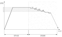
도 2는 실시예에 따른 웨이퍼 제조 방법을 설명하기 위한 그래프이다.
Claims (4)
- 성장 온도에서 웨이퍼 표면에 에피층이 성장하는 단계; 및
상기 에피층의 성장 후, 냉각하는 단계를 포함하고,
상기 냉각하는 단계에서는 단계적 냉각이 이루어지는 웨이퍼 제조 방법. - 제1항에 있어서,
상기 단계적 냉각은 0.1 ℃/h 내지 10 ℃/h 의 속도로 이루어지는 웨이퍼 제조 방법. - 제1항에 있어서,
상기 냉각하는 단계는 제1 온도까지 냉각하는 단계, 상기 제1 온도에서 유지하는 단계, 상기 제1 온도보다 낮은 제2 온도까지 냉각하는 단계, 상기 제2 온도에서 유지하는 단계, 상기 제2 온도보다 낮은 제3 온도까지 냉각하는 단계 및 상기 제3 온도에서 유지하는 단계를 포함하는 웨이퍼 제조 방법. - 제3항에 있어서,
상기 냉각하는 단계는 상기 제3 온도보다 낮은 제4 온도까지 냉각하는 단계 및 상기 제4 온도에서 유지하는 단계를 더 포함하는 웨이퍼 제조 방법
Priority Applications (3)
| Application Number | Priority Date | Filing Date | Title |
|---|---|---|---|
| KR1020110060906A KR101905860B1 (ko) | 2011-06-22 | 2011-06-22 | 웨이퍼 제조 방법 |
| PCT/KR2012/004963 WO2012177086A2 (en) | 2011-06-22 | 2012-06-22 | Method of fabricating wafer |
| US14/128,855 US9745667B2 (en) | 2011-06-22 | 2012-06-22 | Method of fabricating wafer |
Applications Claiming Priority (1)
| Application Number | Priority Date | Filing Date | Title |
|---|---|---|---|
| KR1020110060906A KR101905860B1 (ko) | 2011-06-22 | 2011-06-22 | 웨이퍼 제조 방법 |
Publications (2)
| Publication Number | Publication Date |
|---|---|
| KR20130000296A true KR20130000296A (ko) | 2013-01-02 |
| KR101905860B1 KR101905860B1 (ko) | 2018-11-28 |
Family
ID=47833914
Family Applications (1)
| Application Number | Title | Priority Date | Filing Date |
|---|---|---|---|
| KR1020110060906A Active KR101905860B1 (ko) | 2011-06-22 | 2011-06-22 | 웨이퍼 제조 방법 |
Country Status (1)
| Country | Link |
|---|---|
| KR (1) | KR101905860B1 (ko) |
Family Cites Families (6)
| Publication number | Priority date | Publication date | Assignee | Title |
|---|---|---|---|---|
| US6307241B1 (en) | 1995-06-07 | 2001-10-23 | The Regents Of The Unversity Of California | Integrable ferromagnets for high density storage |
| US6071810A (en) | 1996-12-24 | 2000-06-06 | Kabushiki Kaisha Toshiba | Method of filling contact holes and wiring grooves of a semiconductor device |
| WO2004030073A1 (ja) * | 2002-09-27 | 2004-04-08 | Hitachi Kokusai Electric Inc. | 熱処理装置、半導体装置の製造方法及び基板の製造方法 |
| JP5014737B2 (ja) | 2006-09-21 | 2012-08-29 | 新日本製鐵株式会社 | SiC単結晶基板の製造方法 |
| KR100829927B1 (ko) | 2007-02-08 | 2008-05-16 | 주식회사 비아트론 | 반도체 소자 로딩 모듈 및 이를 이용한 반도체 소자 열처리시스템 |
| US8202788B2 (en) | 2008-06-26 | 2012-06-19 | Nanyang Technological University | Method for fabricating GaNAsSb semiconductor |
-
2011
- 2011-06-22 KR KR1020110060906A patent/KR101905860B1/ko active Active
Also Published As
| Publication number | Publication date |
|---|---|
| KR101905860B1 (ko) | 2018-11-28 |
Similar Documents
| Publication | Publication Date | Title |
|---|---|---|
| KR101971597B1 (ko) | 웨이퍼 및 박막 제조 방법 | |
| KR101430217B1 (ko) | 에피택셜 탄화규소 단결정 기판 및 그 제조 방법 | |
| JP4964672B2 (ja) | 低抵抗率炭化珪素単結晶基板 | |
| US10964785B2 (en) | SiC epitaxial wafer and manufacturing method of the same | |
| KR101951838B1 (ko) | 탄화규소 에피 웨이퍼 제조 방법 | |
| JP2019091798A (ja) | SiCエピタキシャルウェハ | |
| KR102165614B1 (ko) | 에피택셜 웨이퍼 | |
| KR102098297B1 (ko) | 에피택셜 웨이퍼 | |
| KR102565964B1 (ko) | 에피택셜 웨이퍼 및 그 제조 방법 | |
| KR20200075992A (ko) | 탄화규소 에피웨이퍼 제조방법 | |
| US20190164753A1 (en) | Method for fabricating ingap epitaxial layer by metal organic chemical vapor deposition (mocvd) | |
| KR20130000303A (ko) | 웨이퍼 제조 방법 | |
| KR20130000300A (ko) | 웨이퍼 제조 방법 | |
| KR101905860B1 (ko) | 웨이퍼 제조 방법 | |
| KR20130045493A (ko) | 웨이퍼 및 박막 제조 방법 | |
| KR20130000302A (ko) | 웨이퍼 제조 방법 | |
| KR20130000297A (ko) | 웨이퍼 제조 방법 | |
| JP5954677B2 (ja) | III/VSiテンプレートの製造方法およびIII/V半導体ベースの半導体部品をモノリシック集積化する方法 | |
| US9745667B2 (en) | Method of fabricating wafer | |
| KR20140070013A (ko) | 에피택셜 웨이퍼 및 그 제조 방법 | |
| KR102165615B1 (ko) | 에피택셜 웨이퍼 | |
| KR20140100121A (ko) | 에피택셜 웨이퍼 및 그 제조 방법 | |
| JP2021082641A (ja) | エピタキシャルウェーハの製造方法及びエピタキシャルウェーハ | |
| KR20150025648A (ko) | 에피택셜 웨이퍼 | |
| KR102128495B1 (ko) | 에피택셜 웨이퍼 |
Legal Events
| Date | Code | Title | Description |
|---|---|---|---|
| PA0109 | Patent application |
St.27 status event code: A-0-1-A10-A12-nap-PA0109 |
|
| PG1501 | Laying open of application |
St.27 status event code: A-1-1-Q10-Q12-nap-PG1501 |
|
| PN2301 | Change of applicant |
St.27 status event code: A-3-3-R10-R13-asn-PN2301 St.27 status event code: A-3-3-R10-R11-asn-PN2301 |
|
| R17-X000 | Change to representative recorded |
St.27 status event code: A-3-3-R10-R17-oth-X000 |
|
| A201 | Request for examination | ||
| PA0201 | Request for examination |
St.27 status event code: A-1-2-D10-D11-exm-PA0201 |
|
| R18-X000 | Changes to party contact information recorded |
St.27 status event code: A-3-3-R10-R18-oth-X000 |
|
| P22-X000 | Classification modified |
St.27 status event code: A-2-2-P10-P22-nap-X000 |
|
| E902 | Notification of reason for refusal | ||
| PE0902 | Notice of grounds for rejection |
St.27 status event code: A-1-2-D10-D21-exm-PE0902 |
|
| R17-X000 | Change to representative recorded |
St.27 status event code: A-3-3-R10-R17-oth-X000 |
|
| E13-X000 | Pre-grant limitation requested |
St.27 status event code: A-2-3-E10-E13-lim-X000 |
|
| P11-X000 | Amendment of application requested |
St.27 status event code: A-2-2-P10-P11-nap-X000 |
|
| P13-X000 | Application amended |
St.27 status event code: A-2-2-P10-P13-nap-X000 |
|
| E701 | Decision to grant or registration of patent right | ||
| PE0701 | Decision of registration |
St.27 status event code: A-1-2-D10-D22-exm-PE0701 |
|
| R18-X000 | Changes to party contact information recorded |
St.27 status event code: A-3-3-R10-R18-oth-X000 |
|
| GRNT | Written decision to grant | ||
| PR0701 | Registration of establishment |
St.27 status event code: A-2-4-F10-F11-exm-PR0701 |
|
| PR1002 | Payment of registration fee |
St.27 status event code: A-2-2-U10-U11-oth-PR1002 Fee payment year number: 1 |
|
| PG1601 | Publication of registration |
St.27 status event code: A-4-4-Q10-Q13-nap-PG1601 |
|
| R18-X000 | Changes to party contact information recorded |
St.27 status event code: A-5-5-R10-R18-oth-X000 |
|
| PN2301 | Change of applicant |
St.27 status event code: A-5-5-R10-R13-asn-PN2301 St.27 status event code: A-5-5-R10-R11-asn-PN2301 |
|
| PR1001 | Payment of annual fee |
St.27 status event code: A-4-4-U10-U11-oth-PR1001 Fee payment year number: 4 |
|
| PN2301 | Change of applicant |
St.27 status event code: A-5-5-R10-R11-asn-PN2301 |
|
| PN2301 | Change of applicant |
St.27 status event code: A-5-5-R10-R14-asn-PN2301 |
|
| PR1001 | Payment of annual fee |
St.27 status event code: A-4-4-U10-U11-oth-PR1001 Fee payment year number: 5 |
|
| R17-X000 | Change to representative recorded |
St.27 status event code: A-5-5-R10-R17-oth-X000 |
|
| PR1001 | Payment of annual fee |
St.27 status event code: A-4-4-U10-U11-oth-PR1001 Fee payment year number: 6 |
|
| PR1001 | Payment of annual fee |
St.27 status event code: A-4-4-U10-U11-oth-PR1001 Fee payment year number: 7 |
|
| PR1001 | Payment of annual fee |
St.27 status event code: A-4-4-U10-U11-oth-PR1001 Fee payment year number: 8 |