KR20120091368A - 주입된 측벽들을 가지는 반도체 장치들의 제조 방법 및 그에 의해 제조된 장치들 - Google Patents
주입된 측벽들을 가지는 반도체 장치들의 제조 방법 및 그에 의해 제조된 장치들 Download PDFInfo
- Publication number
- KR20120091368A KR20120091368A KR1020127015489A KR20127015489A KR20120091368A KR 20120091368 A KR20120091368 A KR 20120091368A KR 1020127015489 A KR1020127015489 A KR 1020127015489A KR 20127015489 A KR20127015489 A KR 20127015489A KR 20120091368 A KR20120091368 A KR 20120091368A
- Authority
- KR
- South Korea
- Prior art keywords
- layer
- regions
- source
- channel
- channel layer
- Prior art date
- Legal status (The legal status is an assumption and is not a legal conclusion. Google has not performed a legal analysis and makes no representation as to the accuracy of the status listed.)
- Withdrawn
Links
Images


Classifications
-
- H—ELECTRICITY
- H01—ELECTRIC ELEMENTS
- H01L—SEMICONDUCTOR DEVICES NOT COVERED BY CLASS H10
- H01L21/00—Processes or apparatus adapted for the manufacture or treatment of semiconductor or solid state devices or of parts thereof
- H01L21/02—Manufacture or treatment of semiconductor devices or of parts thereof
- H01L21/04—Manufacture or treatment of semiconductor devices or of parts thereof the devices having potential barriers, e.g. a PN junction, depletion layer or carrier concentration layer
- H01L21/0445—Manufacture or treatment of semiconductor devices or of parts thereof the devices having potential barriers, e.g. a PN junction, depletion layer or carrier concentration layer the devices having semiconductor bodies comprising crystalline silicon carbide
- H01L21/0455—Making n or p doped regions or layers, e.g. using diffusion
- H01L21/046—Making n or p doped regions or layers, e.g. using diffusion using ion implantation
- H01L21/047—Making n or p doped regions or layers, e.g. using diffusion using ion implantation characterised by the angle between the ion beam and the crystal planes or the main crystal surface
-
- H—ELECTRICITY
- H10—SEMICONDUCTOR DEVICES; ELECTRIC SOLID-STATE DEVICES NOT OTHERWISE PROVIDED FOR
- H10D—INORGANIC ELECTRIC SEMICONDUCTOR DEVICES
- H10D12/00—Bipolar devices controlled by the field effect, e.g. insulated-gate bipolar transistors [IGBT]
- H10D12/01—Manufacture or treatment
- H10D12/031—Manufacture or treatment of IGBTs
-
- H—ELECTRICITY
- H10—SEMICONDUCTOR DEVICES; ELECTRIC SOLID-STATE DEVICES NOT OTHERWISE PROVIDED FOR
- H10D—INORGANIC ELECTRIC SEMICONDUCTOR DEVICES
- H10D30/00—Field-effect transistors [FET]
- H10D30/80—FETs having rectifying junction gate electrodes
- H10D30/83—FETs having PN junction gate electrodes
- H10D30/831—Vertical FETs having PN junction gate electrodes
-
- H—ELECTRICITY
- H10—SEMICONDUCTOR DEVICES; ELECTRIC SOLID-STATE DEVICES NOT OTHERWISE PROVIDED FOR
- H10D—INORGANIC ELECTRIC SEMICONDUCTOR DEVICES
- H10D62/00—Semiconductor bodies, or regions thereof, of devices having potential barriers
- H10D62/10—Shapes, relative sizes or dispositions of the regions of the semiconductor bodies; Shapes of the semiconductor bodies
- H10D62/17—Semiconductor regions connected to electrodes not carrying current to be rectified, amplified or switched, e.g. channel regions
- H10D62/343—Gate regions of field-effect devices having PN junction gates
-
- H—ELECTRICITY
- H10—SEMICONDUCTOR DEVICES; ELECTRIC SOLID-STATE DEVICES NOT OTHERWISE PROVIDED FOR
- H10D—INORGANIC ELECTRIC SEMICONDUCTOR DEVICES
- H10D62/00—Semiconductor bodies, or regions thereof, of devices having potential barriers
- H10D62/80—Semiconductor bodies, or regions thereof, of devices having potential barriers characterised by the materials
- H10D62/83—Semiconductor bodies, or regions thereof, of devices having potential barriers characterised by the materials being Group IV materials, e.g. B-doped Si or undoped Ge
- H10D62/832—Semiconductor bodies, or regions thereof, of devices having potential barriers characterised by the materials being Group IV materials, e.g. B-doped Si or undoped Ge being Group IV materials comprising two or more elements, e.g. SiGe
- H10D62/8325—Silicon carbide
Landscapes
- Chemical & Material Sciences (AREA)
- Crystallography & Structural Chemistry (AREA)
- Engineering & Computer Science (AREA)
- Physics & Mathematics (AREA)
- Condensed Matter Physics & Semiconductors (AREA)
- General Physics & Mathematics (AREA)
- Manufacturing & Machinery (AREA)
- Computer Hardware Design (AREA)
- Microelectronics & Electronic Packaging (AREA)
- Power Engineering (AREA)
- Junction Field-Effect Transistors (AREA)
Applications Claiming Priority (2)
| Application Number | Priority Date | Filing Date | Title |
|---|---|---|---|
| US26752409P | 2009-12-08 | 2009-12-08 | |
| US61/267,524 | 2009-12-08 |
Publications (1)
| Publication Number | Publication Date |
|---|---|
| KR20120091368A true KR20120091368A (ko) | 2012-08-17 |
Family
ID=44081165
Family Applications (1)
| Application Number | Title | Priority Date | Filing Date |
|---|---|---|---|
| KR1020127015489A Withdrawn KR20120091368A (ko) | 2009-12-08 | 2010-12-08 | 주입된 측벽들을 가지는 반도체 장치들의 제조 방법 및 그에 의해 제조된 장치들 |
Country Status (8)
Cited By (1)
| Publication number | Priority date | Publication date | Assignee | Title |
|---|---|---|---|---|
| KR20160066811A (ko) * | 2014-12-03 | 2016-06-13 | 서강대학교산학협력단 | 경사 이온 주입을 이용한 실리콘 카바이드 트렌치 모스 장벽 쇼트키 다이오드 및 그의 제조 방법 |
Families Citing this family (19)
| Publication number | Priority date | Publication date | Assignee | Title |
|---|---|---|---|---|
| AU2010262789A1 (en) * | 2009-06-19 | 2012-02-02 | Power Integrations, Inc. | Methods of making vertical junction field effect transistors and bipolar junction transistors without ion implantation and devices made therewith |
| US8969912B2 (en) | 2011-08-04 | 2015-03-03 | Avogy, Inc. | Method and system for a GaN vertical JFET utilizing a regrown channel |
| US9136116B2 (en) * | 2011-08-04 | 2015-09-15 | Avogy, Inc. | Method and system for formation of P-N junctions in gallium nitride based electronics |
| CN103946978B (zh) * | 2011-11-24 | 2017-03-01 | 夏普株式会社 | 半导体装置以及电子设备 |
| US8969994B2 (en) * | 2012-08-14 | 2015-03-03 | Avogy, Inc. | Method of fabricating a gallium nitride merged P-i-N Schottky (MPS) diode by regrowth and etch back |
| US8937317B2 (en) | 2012-12-28 | 2015-01-20 | Avogy, Inc. | Method and system for co-packaging gallium nitride electronics |
| US9324645B2 (en) | 2013-05-23 | 2016-04-26 | Avogy, Inc. | Method and system for co-packaging vertical gallium nitride power devices |
| US9136397B2 (en) | 2013-05-31 | 2015-09-15 | Infineon Technologies Ag | Field-effect semiconductor device |
| JP6138619B2 (ja) * | 2013-07-30 | 2017-05-31 | ルネサスエレクトロニクス株式会社 | 半導体装置の製造方法および半導体装置 |
| US8947154B1 (en) | 2013-10-03 | 2015-02-03 | Avogy, Inc. | Method and system for operating gallium nitride electronics |
| US9184281B2 (en) * | 2013-10-30 | 2015-11-10 | Infineon Technologies Ag | Method for manufacturing a vertical semiconductor device and vertical semiconductor device |
| US9324809B2 (en) | 2013-11-18 | 2016-04-26 | Avogy, Inc. | Method and system for interleaved boost converter with co-packaged gallium nitride power devices |
| US9543290B2 (en) | 2014-01-23 | 2017-01-10 | International Business Machines Corporation | Normally-off junction field-effect transistors and application to complementary circuits |
| US20160268446A1 (en) * | 2015-03-10 | 2016-09-15 | United Silicon Carbide, Inc. | Trench vertical jfet with improved threshold voltage control |
| US10396215B2 (en) | 2015-03-10 | 2019-08-27 | United Silicon Carbide, Inc. | Trench vertical JFET with improved threshold voltage control |
| US9905645B2 (en) | 2016-05-24 | 2018-02-27 | Samsung Electronics Co., Ltd. | Vertical field effect transistor having an elongated channel |
| CN109791951B (zh) * | 2016-09-09 | 2023-08-01 | 美国联合碳化硅公司 | 具有改进的阈值电压控制的沟槽垂直jfet |
| KR102314006B1 (ko) * | 2017-09-11 | 2021-10-18 | 삼성전자주식회사 | 수직 전계 트랜지스터 및 이를 포함하는 반도체 장치 |
| CN112909088B (zh) * | 2021-01-25 | 2022-11-08 | 深圳大学 | 静电感应晶体管及其制备方法 |
Family Cites Families (16)
| Publication number | Priority date | Publication date | Assignee | Title |
|---|---|---|---|---|
| JPS60247921A (ja) * | 1984-05-23 | 1985-12-07 | Toshiba Corp | 半導体装置の製造方法 |
| JPS61154029A (ja) * | 1984-12-26 | 1986-07-12 | Nec Corp | ボロンのド−ピング方法 |
| DE4423068C1 (de) * | 1994-07-01 | 1995-08-17 | Daimler Benz Ag | Feldeffekt-Transistoren aus SiC und Verfahren zu ihrer Herstellung |
| JPH10163313A (ja) * | 1996-11-26 | 1998-06-19 | New Japan Radio Co Ltd | 半導体装置の製造方法 |
| US5903020A (en) * | 1997-06-18 | 1999-05-11 | Northrop Grumman Corporation | Silicon carbide static induction transistor structure |
| US6509240B2 (en) * | 2000-05-15 | 2003-01-21 | International Rectifier Corporation | Angle implant process for cellular deep trench sidewall doping |
| US6713351B2 (en) * | 2001-03-28 | 2004-03-30 | General Semiconductor, Inc. | Double diffused field effect transistor having reduced on-resistance |
| EP1267210B1 (en) | 2001-06-12 | 2018-02-21 | FUJIFILM Corporation | Positive resist composition |
| WO2003075319A2 (en) * | 2001-07-12 | 2003-09-12 | Mississippi State University | Self-aligned transistor and diode topologies |
| JP2004134547A (ja) * | 2002-10-10 | 2004-04-30 | Hitachi Ltd | 半導体装置 |
| US6821834B2 (en) * | 2002-12-04 | 2004-11-23 | Yoshiyuki Ando | Ion implantation methods and transistor cell layout for fin type transistors |
| US20050067630A1 (en) * | 2003-09-25 | 2005-03-31 | Zhao Jian H. | Vertical junction field effect power transistor |
| US20060046392A1 (en) * | 2004-08-26 | 2006-03-02 | Manning H M | Methods of forming vertical transistor structures |
| US7355223B2 (en) * | 2005-03-04 | 2008-04-08 | Cree, Inc. | Vertical junction field effect transistor having an epitaxial gate |
| US7550787B2 (en) * | 2005-05-31 | 2009-06-23 | International Business Machines Corporation | Varied impurity profile region formation for varying breakdown voltage of devices |
| US7977713B2 (en) * | 2008-05-08 | 2011-07-12 | Semisouth Laboratories, Inc. | Semiconductor devices with non-punch-through semiconductor channels having enhanced conduction and methods of making |
-
2010
- 2010-12-08 EP EP20100836585 patent/EP2510539A4/en not_active Withdrawn
- 2010-12-08 JP JP2012543225A patent/JP2013513252A/ja active Pending
- 2010-12-08 CN CN2010800553654A patent/CN102648514A/zh active Pending
- 2010-12-08 AU AU2010328256A patent/AU2010328256A1/en not_active Abandoned
- 2010-12-08 US US12/962,823 patent/US8466017B2/en not_active Expired - Fee Related
- 2010-12-08 CA CA2780459A patent/CA2780459A1/en not_active Abandoned
- 2010-12-08 KR KR1020127015489A patent/KR20120091368A/ko not_active Withdrawn
- 2010-12-08 WO PCT/US2010/059374 patent/WO2011071973A2/en active Application Filing
Cited By (1)
| Publication number | Priority date | Publication date | Assignee | Title |
|---|---|---|---|---|
| KR20160066811A (ko) * | 2014-12-03 | 2016-06-13 | 서강대학교산학협력단 | 경사 이온 주입을 이용한 실리콘 카바이드 트렌치 모스 장벽 쇼트키 다이오드 및 그의 제조 방법 |
Also Published As
| Publication number | Publication date |
|---|---|
| EP2510539A2 (en) | 2012-10-17 |
| US20110133212A1 (en) | 2011-06-09 |
| AU2010328256A1 (en) | 2012-06-21 |
| CN102648514A (zh) | 2012-08-22 |
| US8466017B2 (en) | 2013-06-18 |
| JP2013513252A (ja) | 2013-04-18 |
| EP2510539A4 (en) | 2013-07-31 |
| WO2011071973A2 (en) | 2011-06-16 |
| CA2780459A1 (en) | 2011-06-16 |
| WO2011071973A3 (en) | 2011-10-27 |
Similar Documents
| Publication | Publication Date | Title |
|---|---|---|
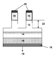
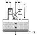
| US8466017B2 (en) | Methods of making semiconductor devices having implanted sidewalls and devices made thereby | |
| US20210183995A1 (en) | Superjunction silicon carbide semiconductor device and method of manufacturing superjunction silicon carbide semiconductor device | |
| US7829402B2 (en) | MOSFET devices and methods of making | |
| US8169022B2 (en) | Vertical junction field effect transistors and diodes having graded doped regions and methods of making | |
| CN102239563B (zh) | 具有倾斜侧壁的垂向结型场效应晶体管及其制造方法 | |
| CN103477439B (zh) | 半导体装置及其制造方法 | |
| US20180145168A1 (en) | Silicon-carbide trench gate mosfets and methods of manufacture | |
| KR20020071954A (ko) | 반도체장치 및 그 제조방법 | |
| KR101830174B1 (ko) | 전계제한링이 형성된 전력반도체용 소자 및 그 제조방법 | |
| WO2013001677A1 (ja) | 半導体装置とその製造方法 | |
| US8659057B2 (en) | Self-aligned semiconductor devices with reduced gate-source leakage under reverse bias and methods of making | |
| US20180040690A1 (en) | Semiconductor device and method of manufacturing semiconductor device | |
| US7772613B2 (en) | Semiconductor device with large blocking voltage and method of manufacturing the same | |
| US20090159896A1 (en) | Silicon carbide mosfet devices and methods of making | |
| JP2023110083A (ja) | グリッドを製造するための方法 | |
| JP6211933B2 (ja) | 半導体装置 | |
| KR102285500B1 (ko) | 탄화규소 스위치 소자 및 제작방법 | |
| JP3637052B2 (ja) | SiC−MISFET及びその製造方法 | |
| JP7055537B2 (ja) | 半導体デバイスおよびその製作方法 |
Legal Events
| Date | Code | Title | Description |
|---|---|---|---|
| PA0105 | International application |
Patent event date: 20120615 Patent event code: PA01051R01D Comment text: International Patent Application |
|
| PG1501 | Laying open of application | ||
| N231 | Notification of change of applicant | ||
| PN2301 | Change of applicant |
Patent event date: 20130917 Comment text: Notification of Change of Applicant Patent event code: PN23011R01D |
|
| PC1203 | Withdrawal of no request for examination | ||
| WITN | Application deemed withdrawn, e.g. because no request for examination was filed or no examination fee was paid |