US8466017B2 - Methods of making semiconductor devices having implanted sidewalls and devices made thereby - Google Patents
Methods of making semiconductor devices having implanted sidewalls and devices made thereby Download PDFInfo
- Publication number
- US8466017B2 US8466017B2 US12/962,823 US96282310A US8466017B2 US 8466017 B2 US8466017 B2 US 8466017B2 US 96282310 A US96282310 A US 96282310A US 8466017 B2 US8466017 B2 US 8466017B2
- Authority
- US
- United States
- Prior art keywords
- layer
- channel layer
- implant mask
- ions
- implanted
- Prior art date
- Legal status (The legal status is an assumption and is not a legal conclusion. Google has not performed a legal analysis and makes no representation as to the accuracy of the status listed.)
- Expired - Fee Related, expires
Links
Images


Classifications
-
- H—ELECTRICITY
- H01—ELECTRIC ELEMENTS
- H01L—SEMICONDUCTOR DEVICES NOT COVERED BY CLASS H10
- H01L21/00—Processes or apparatus adapted for the manufacture or treatment of semiconductor or solid state devices or of parts thereof
- H01L21/02—Manufacture or treatment of semiconductor devices or of parts thereof
- H01L21/04—Manufacture or treatment of semiconductor devices or of parts thereof the devices having potential barriers, e.g. a PN junction, depletion layer or carrier concentration layer
- H01L21/0445—Manufacture or treatment of semiconductor devices or of parts thereof the devices having potential barriers, e.g. a PN junction, depletion layer or carrier concentration layer the devices having semiconductor bodies comprising crystalline silicon carbide
- H01L21/0455—Making n or p doped regions or layers, e.g. using diffusion
- H01L21/046—Making n or p doped regions or layers, e.g. using diffusion using ion implantation
- H01L21/047—Making n or p doped regions or layers, e.g. using diffusion using ion implantation characterised by the angle between the ion beam and the crystal planes or the main crystal surface
-
- H—ELECTRICITY
- H10—SEMICONDUCTOR DEVICES; ELECTRIC SOLID-STATE DEVICES NOT OTHERWISE PROVIDED FOR
- H10D—INORGANIC ELECTRIC SEMICONDUCTOR DEVICES
- H10D12/00—Bipolar devices controlled by the field effect, e.g. insulated-gate bipolar transistors [IGBT]
- H10D12/01—Manufacture or treatment
- H10D12/031—Manufacture or treatment of IGBTs
-
- H—ELECTRICITY
- H10—SEMICONDUCTOR DEVICES; ELECTRIC SOLID-STATE DEVICES NOT OTHERWISE PROVIDED FOR
- H10D—INORGANIC ELECTRIC SEMICONDUCTOR DEVICES
- H10D30/00—Field-effect transistors [FET]
- H10D30/80—FETs having rectifying junction gate electrodes
- H10D30/83—FETs having PN junction gate electrodes
- H10D30/831—Vertical FETs having PN junction gate electrodes
-
- H—ELECTRICITY
- H10—SEMICONDUCTOR DEVICES; ELECTRIC SOLID-STATE DEVICES NOT OTHERWISE PROVIDED FOR
- H10D—INORGANIC ELECTRIC SEMICONDUCTOR DEVICES
- H10D62/00—Semiconductor bodies, or regions thereof, of devices having potential barriers
- H10D62/10—Shapes, relative sizes or dispositions of the regions of the semiconductor bodies; Shapes of the semiconductor bodies
- H10D62/17—Semiconductor regions connected to electrodes not carrying current to be rectified, amplified or switched, e.g. channel regions
- H10D62/343—Gate regions of field-effect devices having PN junction gates
-
- H—ELECTRICITY
- H10—SEMICONDUCTOR DEVICES; ELECTRIC SOLID-STATE DEVICES NOT OTHERWISE PROVIDED FOR
- H10D—INORGANIC ELECTRIC SEMICONDUCTOR DEVICES
- H10D62/00—Semiconductor bodies, or regions thereof, of devices having potential barriers
- H10D62/80—Semiconductor bodies, or regions thereof, of devices having potential barriers characterised by the materials
- H10D62/83—Semiconductor bodies, or regions thereof, of devices having potential barriers characterised by the materials being Group IV materials, e.g. B-doped Si or undoped Ge
- H10D62/832—Semiconductor bodies, or regions thereof, of devices having potential barriers characterised by the materials being Group IV materials, e.g. B-doped Si or undoped Ge being Group IV materials comprising two or more elements, e.g. SiGe
- H10D62/8325—Silicon carbide
Definitions
- This application relates generally to semiconductor devices and to methods of making the devices.
- a field-effect transistor is a type of transistor commonly used for weak-signal amplification (e.g., for amplifying wireless signals).
- the device can amplify analog or digital signals. It can also switch DC or function as an oscillator.
- current flows along a semiconductor path called the channel. At one end of the channel, there is an electrode called the source. At the other end of the channel, there is an electrode called the drain.
- the physical diameter of the channel is fixed, but its effective electrical diameter can be varied by the application of a voltage to a control electrode called the gate.
- the conductivity of the FET depends, at any given instant in time, on the electrical diameter of the channel. A small change in gate voltage can cause a large variation in the current from the source to the drain thereby allowing for amplification of signals.
- a PiN diode is a diode with a wide, lightly doped ‘near’ intrinsic semiconductor region between p-type semiconductor and n-type semiconductor regions.
- a junction barrier Schottky (JBS) diode is also referred to as a merged PiN Schottky diode since it contains both PiN and Schottky barrier (i.e., metal-semiconductor) junctions.
- VJFET Vertical Junction Field Effect Transistor
- SIT Static Induction Transistor
- angled implantation on the source finger sidewalls is disclosed as a method to create a long gate doping profile along the source channel length.
- This method has several disadvantages, however. Namely, the wafer has to be rotated during implantation in order to prevent implant shadowing in the trenched structure. Additionally, the angled implant causes uniform implantation along the vertical axis of the structure from the channel into the source region causing two adjoining heavily doped regions (source and gate). The close nature of these two regions result in poor voltage handling capability. Additionally, angled implantation along this axis can create significant channeling of the ions resulting in a non-symmetrical gate-source junction, particularly for SiC substrates which are typically cut off-axis (e.g., at an angle of 2-8 degrees).
- a method of making a semiconductor device which comprises:
- the implant mask layer is on a channel layer of a semiconductor material of a first conductivity type and wherein the channel layer is on an upper surface of a semiconductor substrate of the first conductivity type;
- a semiconductor device made by a method as set forth above is also provided.
- FIGS. 1A-1E are schematics illustrating the manufacture of a VJFET device wherein:
- FIG. 1A shows the starting device structure prior to implantation
- FIG. 1B shows the deposition of a patterned etch mask that will be used to define the width and pitch of the source fingers
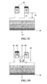
- FIG. 1C shows the etching of the implant mask and channel layer
- FIG. 1D shows the implantation of the p+ gate using ion implantation at an angle of 0° (i.e., perpendicular to the substrate surface)
- FIG. 1E shows the resulting dopant profile in the device after implantation and removal of the implant mask.
- FIG. 2 is a schematic showing the top view of an exemplary layout of a source finger array having a periodic array structure which allows sufficient scattering implantation on the sidewalls of each source finger.
- FIG. 3A is simulation showing the dopant profile resulting from near vertical implantation into a trenched structure with sufficient implant mask and finger pitch to allow significant scattering implantation to occur and dope the sidewalls.
- FIG. 3B is simulation conducted under similar conditions as that of FIG. 3A but wherein the device does not have an adjacent source finger to provide ion scattering.
- FIG. 4 is a graph showing the effect of scattering on the threshold voltage of a SiC VJFET.
- VJFET Vertical Junction Field Effect Transistor
- the invention can be applicable to any vertical device that has an exposed sidewall requiring implantation (e.g., diode, transistor, vertical resistor), the specific embodiment of this invention enables a long channel VJFET that can be made in either the enhancement or depletion mode.
- the long channel of the device enables a high ‘blocking gain’ (a sharp transition from forward conduction to reverse blocking stage) while maintaining a long high-potential barrier to leakage currents from drain to source under high reverse bias.
- a trench and masking structure to create an ion implantation (i.e., doping) profile on a vertical trench sidewall in a semiconductor device are described.
- a long trenched channel Vertical Junction Field Effect Transistor in SiC is provided wherein angled sidewall implantation is not employed.
- the scattering of ions out by a masking layer creates a doping profile on the edge of a trenched semiconductor sidewall.
- the methods described herein can be used in the gate region of a VJFET. However, the methods described herein can be used to make any semiconductor structure which would benefit from an implanted sidewall, including, but not limited to, static induction transistors (SITs), bipolar junction transistors (BJTs), and junction-barrier Schottky diodes (JBS).
- SITs static induction transistors
- BJTs bipolar junction transistors
- JBS junction-barrier Schottky diodes
- FIGS. 1A-1E A method of making a VJFET is depicted in FIGS. 1A-1E and described below.
- FIG. 1A shows the starting semiconductor structure prior to implantation process.
- the device prior to implantation comprises an implant mask layer 10 on channel layer 12 .
- channel layer 12 is on drift layer 14 and drift layer 14 is on semiconductor substrate 16 .
- Drain contact 18 is shown on substrate opposite drift layer 14 .
- the drift layer is optional (i.e., the channel and drift layers can be a single layer).
- Drift layer 14 and channel layer 12 can be epitaxially grown.
- the doping type and concentration can be varied to provide desired characteristics for the device.
- the substrate can be n-type with a nitrogen doping concentration of 1 ⁇ 10 18 /cm 3 to 1 ⁇ 10 20 /cm 3 .
- the drift and channel nitrogen doping levels can be between 1 ⁇ 10 14 /cm 3 and 1 ⁇ 10 18 /cm 3 .
- the thickness of the drift layer can be ⁇ 100 ⁇ m and the thickness of the channel layer can be between 0.25 ⁇ m and 5 ⁇ m.
- n+ cap layer (not shown) on top of channel layer 12 .
- the implantation mask can be any of a variety of materials including a photoresist material, an oxide, a nitride, and deposited metals.
- the thickness of the implant masking material can be >0.5 ⁇ m.
- the thickness of the implant masking material can be varied depending upon the height of the semiconductor trench structure.
- FIG. 1B shows the deposition of patterned etch mask 20 on implant mask layer 10 .
- Patterned etch mask 20 is used to define the source finger width and pitch.
- the material used for patterned etch mask 20 can be a conventional semiconductor etch mask material such as an oxide, a metal, or a photoresist.
- FIG. 1C is a schematic showing implant mask layer 10 and channel layer 12 being selectively etched using etch mask 20 .
- the etch process will be performed by a dry Reactive Ion Etch (RIE) or Inductively Coupled Plasma (ICP) based plasma etch.
- RIE reactive ion Etch
- ICP Inductively Coupled Plasma
- the etching will continue through the implant/etch mask and continue to etch the SiC of channel layer 12 to a predetermined depth.
- the height of the etched channel 22 will be dependent on the design of the device.
- An exemplary etched channel height is 0.25 to 5 ⁇ m.
- the implantation 24 of the p+ gate is performed using ion implantation at 0 degrees. Although 0° implantation is shown, alternate slight angles can be used. When an angled implantation is employed, the wafer can be rotated during the implantation process.
- the ions arrive at the structure at an angle of 0 degrees (i.e., perpendicular to the wafer surface) and either enter the semiconductor surface between the source fingers thereby creating the bottom of the gate profile, or enter the implantation mask on top of the source fingers.
- Some of the ions that enter the implantation mask will encounter a scattering event and will have enough energy to exit the implantation mask at an angle that results in the ion being implanted in the source finger sidewall.
- the implantation dose and energy are variable depending on the amount and depth of the intended sidewall implantation. To have a deeper junction, the implantation energy should be high (e.g., 250 keV-2 MeV).
- FIG. 1E is a schematic cross-sectional view of the device showing the resultant doping profile after the implantation and removal of implant mask 20 .
- a p+ implanted regions are now formed along the sidewalls of the source fingers and at the bottom of the finger.
- the implanted sidewall regions are connected to the implanted region at the bottom of the trenches. This enables a long channel length 32 along the sidewall of the source fingers. This is compared to the short channel described in U.S. Pat. No. 5,903,020, wherein the implantation is only at the bottom of the trench which results in a short channel device optimum for a SIT device.
- the subsequent processing can include implant activation and contact formation on the gate 30 , drain 19 , and source 28 of the device.
- FIG. 2 is a schematic top down view of a device having a source finger array with a periodic array structure which allows sufficient scattering implantation on each source finger.
- the structure is shown as a vertical array, but can be circular, hexagonal, etc, as long as there is an adjacent structure that causes scattering of the implantation into a sidewall.
- Implant can be tilted 0-10 degrees and the substrate can be rotated during the implantation process to ensure that all sides of the structure are equally doped.
- the dopant concentrations and thicknesses of the various layers of the device described herein can be varied to produce a device having desired characteristics for a particular application.
- the dimensions of the various features of the device can also be varied to produce a device having desired characteristics for a particular application.
- the layers of semiconductor material can be formed by epitaxial growth on a suitable substrate.
- the layers can be doped during epitaxial growth.
- FIG. 3A shows a simulation of the doping profile using near vertical implantation into a trenched SiC structure with sufficient implant mask and finger pitch to allow significant scattering implantation to occur and dope the sidewalls.
- the sidewall doping creates a long channel that extends from the bottom of the trench to near the top of the semiconductor surface.
- FIG. 3B is the same simulation as FIG. 3A but without the adjacent scattering finger to provide the ion scattering. Notice that there is minimal implantation on the sidewall of the source finger resulting in a short channel.
- FIG. 4 is a graph showing the effect of scattering on the threshold voltage of a SiC VJFET.
- the threshold voltage of the device As can be seen from FIG. 4 , as the trench spacing is increased, the threshold voltage of the device is reduced. While not wishing to be bound by theory, this phenomenon is believed to be due to the reduction of sidewall dose scattered off the adjacent finger profile as the trench spacing is increased. Conversely, the threshold voltage as shown in FIG. 4 increases as the trench spacing is reduced as a result of the increased implant scattering causing a higher level of doping (and longer channel) on all adjacent fingers.
- the implant mask thickness can be in the range of 0.5 ⁇ m to 5 ⁇ m and can be composed of oxide, photoresist, metal layers, or multilayer stacks suitable for implant blocking at the applicable implant energy.
- the implant energy used to optimize the scattering effect can range from 60 keV-380 keV for shorter fingers and closely spaced trench structures to 1 MeV for deep and uniform implantation where significant scattering effects are desired.
Landscapes
- Chemical & Material Sciences (AREA)
- Crystallography & Structural Chemistry (AREA)
- Engineering & Computer Science (AREA)
- Physics & Mathematics (AREA)
- Condensed Matter Physics & Semiconductors (AREA)
- General Physics & Mathematics (AREA)
- Manufacturing & Machinery (AREA)
- Computer Hardware Design (AREA)
- Microelectronics & Electronic Packaging (AREA)
- Power Engineering (AREA)
- Junction Field-Effect Transistors (AREA)
Priority Applications (1)
| Application Number | Priority Date | Filing Date | Title |
|---|---|---|---|
| US12/962,823 US8466017B2 (en) | 2009-12-08 | 2010-12-08 | Methods of making semiconductor devices having implanted sidewalls and devices made thereby |
Applications Claiming Priority (2)
| Application Number | Priority Date | Filing Date | Title |
|---|---|---|---|
| US26752409P | 2009-12-08 | 2009-12-08 | |
| US12/962,823 US8466017B2 (en) | 2009-12-08 | 2010-12-08 | Methods of making semiconductor devices having implanted sidewalls and devices made thereby |
Publications (2)
| Publication Number | Publication Date |
|---|---|
| US20110133212A1 US20110133212A1 (en) | 2011-06-09 |
| US8466017B2 true US8466017B2 (en) | 2013-06-18 |
Family
ID=44081165
Family Applications (1)
| Application Number | Title | Priority Date | Filing Date |
|---|---|---|---|
| US12/962,823 Expired - Fee Related US8466017B2 (en) | 2009-12-08 | 2010-12-08 | Methods of making semiconductor devices having implanted sidewalls and devices made thereby |
Country Status (8)
Cited By (9)
| Publication number | Priority date | Publication date | Assignee | Title |
|---|---|---|---|---|
| US20130032814A1 (en) * | 2011-08-04 | 2013-02-07 | Epowersoft, Inc. | Method and system for formation of p-n junctions in gallium nitride based electronics |
| US8937317B2 (en) | 2012-12-28 | 2015-01-20 | Avogy, Inc. | Method and system for co-packaging gallium nitride electronics |
| US8947154B1 (en) | 2013-10-03 | 2015-02-03 | Avogy, Inc. | Method and system for operating gallium nitride electronics |
| US9324645B2 (en) | 2013-05-23 | 2016-04-26 | Avogy, Inc. | Method and system for co-packaging vertical gallium nitride power devices |
| US9324809B2 (en) | 2013-11-18 | 2016-04-26 | Avogy, Inc. | Method and system for interleaved boost converter with co-packaged gallium nitride power devices |
| US9324844B2 (en) | 2011-08-04 | 2016-04-26 | Avogy, Inc. | Method and system for a GaN vertical JFET utilizing a regrown channel |
| US9905645B2 (en) | 2016-05-24 | 2018-02-27 | Samsung Electronics Co., Ltd. | Vertical field effect transistor having an elongated channel |
| US10038104B2 (en) | 2014-01-23 | 2018-07-31 | International Business Machines Corporation | Normally-off junction field-effect transistors and application to complementary circuits |
| US10944003B2 (en) | 2017-09-11 | 2021-03-09 | Samsung Electronics Co., Ltd. | Vertical field effect transistor and semiconductor device including the same |
Families Citing this family (11)
| Publication number | Priority date | Publication date | Assignee | Title |
|---|---|---|---|---|
| AU2010262789A1 (en) * | 2009-06-19 | 2012-02-02 | Power Integrations, Inc. | Methods of making vertical junction field effect transistors and bipolar junction transistors without ion implantation and devices made therewith |
| CN103946978B (zh) * | 2011-11-24 | 2017-03-01 | 夏普株式会社 | 半导体装置以及电子设备 |
| US8969994B2 (en) * | 2012-08-14 | 2015-03-03 | Avogy, Inc. | Method of fabricating a gallium nitride merged P-i-N Schottky (MPS) diode by regrowth and etch back |
| US9136397B2 (en) | 2013-05-31 | 2015-09-15 | Infineon Technologies Ag | Field-effect semiconductor device |
| JP6138619B2 (ja) * | 2013-07-30 | 2017-05-31 | ルネサスエレクトロニクス株式会社 | 半導体装置の製造方法および半導体装置 |
| US9184281B2 (en) * | 2013-10-30 | 2015-11-10 | Infineon Technologies Ag | Method for manufacturing a vertical semiconductor device and vertical semiconductor device |
| KR101669987B1 (ko) * | 2014-12-03 | 2016-10-27 | 서강대학교산학협력단 | 경사 이온 주입을 이용한 실리콘 카바이드 트렌치 모스 장벽 쇼트키 다이오드 및 그의 제조 방법 |
| US20160268446A1 (en) * | 2015-03-10 | 2016-09-15 | United Silicon Carbide, Inc. | Trench vertical jfet with improved threshold voltage control |
| US10396215B2 (en) | 2015-03-10 | 2019-08-27 | United Silicon Carbide, Inc. | Trench vertical JFET with improved threshold voltage control |
| CN109791951B (zh) * | 2016-09-09 | 2023-08-01 | 美国联合碳化硅公司 | 具有改进的阈值电压控制的沟槽垂直jfet |
| CN112909088B (zh) * | 2021-01-25 | 2022-11-08 | 深圳大学 | 静电感应晶体管及其制备方法 |
Citations (8)
| Publication number | Priority date | Publication date | Assignee | Title |
|---|---|---|---|---|
| US5903020A (en) | 1997-06-18 | 1999-05-11 | Northrop Grumman Corporation | Silicon carbide static induction transistor structure |
| EP1267210A2 (en) | 2001-06-12 | 2002-12-18 | Fuji Photo Film Co., Ltd. | Positive resist composition |
| US6767783B2 (en) | 2001-07-12 | 2004-07-27 | Mississippi State University-Research And Technology Corporation (Rtc) | Self-aligned transistor and diode topologies in silicon carbide through the use of selective epitaxy or selective implantation |
| US6821834B2 (en) | 2002-12-04 | 2004-11-23 | Yoshiyuki Ando | Ion implantation methods and transistor cell layout for fin type transistors |
| US20060220072A1 (en) * | 2005-03-04 | 2006-10-05 | Christopher Harris | Vertical junction field effect transistor having an epitaxial gate |
| US20060258086A1 (en) | 2004-08-26 | 2006-11-16 | Micron Technology, Inc | Methods of forming vertical transistor structures |
| US20070187715A1 (en) | 2003-09-25 | 2007-08-16 | Zhao Jian H | Power junction field effect power transistor with highly vertical channel and uniform channel opening |
| US20090278177A1 (en) | 2008-05-08 | 2009-11-12 | Semisouth Laboratories, Inc. | Semiconductor devices with non-punch-through semiconductor channels having enhanced conduction and methods of making |
Family Cites Families (8)
| Publication number | Priority date | Publication date | Assignee | Title |
|---|---|---|---|---|
| JPS60247921A (ja) * | 1984-05-23 | 1985-12-07 | Toshiba Corp | 半導体装置の製造方法 |
| JPS61154029A (ja) * | 1984-12-26 | 1986-07-12 | Nec Corp | ボロンのド−ピング方法 |
| DE4423068C1 (de) * | 1994-07-01 | 1995-08-17 | Daimler Benz Ag | Feldeffekt-Transistoren aus SiC und Verfahren zu ihrer Herstellung |
| JPH10163313A (ja) * | 1996-11-26 | 1998-06-19 | New Japan Radio Co Ltd | 半導体装置の製造方法 |
| US6509240B2 (en) * | 2000-05-15 | 2003-01-21 | International Rectifier Corporation | Angle implant process for cellular deep trench sidewall doping |
| US6713351B2 (en) * | 2001-03-28 | 2004-03-30 | General Semiconductor, Inc. | Double diffused field effect transistor having reduced on-resistance |
| JP2004134547A (ja) * | 2002-10-10 | 2004-04-30 | Hitachi Ltd | 半導体装置 |
| US7550787B2 (en) * | 2005-05-31 | 2009-06-23 | International Business Machines Corporation | Varied impurity profile region formation for varying breakdown voltage of devices |
-
2010
- 2010-12-08 EP EP20100836585 patent/EP2510539A4/en not_active Withdrawn
- 2010-12-08 JP JP2012543225A patent/JP2013513252A/ja active Pending
- 2010-12-08 CN CN2010800553654A patent/CN102648514A/zh active Pending
- 2010-12-08 AU AU2010328256A patent/AU2010328256A1/en not_active Abandoned
- 2010-12-08 US US12/962,823 patent/US8466017B2/en not_active Expired - Fee Related
- 2010-12-08 CA CA2780459A patent/CA2780459A1/en not_active Abandoned
- 2010-12-08 KR KR1020127015489A patent/KR20120091368A/ko not_active Withdrawn
- 2010-12-08 WO PCT/US2010/059374 patent/WO2011071973A2/en active Application Filing
Patent Citations (9)
| Publication number | Priority date | Publication date | Assignee | Title |
|---|---|---|---|---|
| US5903020A (en) | 1997-06-18 | 1999-05-11 | Northrop Grumman Corporation | Silicon carbide static induction transistor structure |
| EP1267210A2 (en) | 2001-06-12 | 2002-12-18 | Fuji Photo Film Co., Ltd. | Positive resist composition |
| US6767783B2 (en) | 2001-07-12 | 2004-07-27 | Mississippi State University-Research And Technology Corporation (Rtc) | Self-aligned transistor and diode topologies in silicon carbide through the use of selective epitaxy or selective implantation |
| US6821834B2 (en) | 2002-12-04 | 2004-11-23 | Yoshiyuki Ando | Ion implantation methods and transistor cell layout for fin type transistors |
| US20070187715A1 (en) | 2003-09-25 | 2007-08-16 | Zhao Jian H | Power junction field effect power transistor with highly vertical channel and uniform channel opening |
| US7479672B2 (en) | 2003-09-25 | 2009-01-20 | Rutgers, The State University | Power junction field effect power transistor with highly vertical channel and uniform channel opening |
| US20060258086A1 (en) | 2004-08-26 | 2006-11-16 | Micron Technology, Inc | Methods of forming vertical transistor structures |
| US20060220072A1 (en) * | 2005-03-04 | 2006-10-05 | Christopher Harris | Vertical junction field effect transistor having an epitaxial gate |
| US20090278177A1 (en) | 2008-05-08 | 2009-11-12 | Semisouth Laboratories, Inc. | Semiconductor devices with non-punch-through semiconductor channels having enhanced conduction and methods of making |
Non-Patent Citations (2)
| Title |
|---|
| Hook, Terence B. "Lateral Ion Implant Straggle and Mask Proximity Effect" IEEE Transactions on Electron Devices, vol. 50, No. 9, Sep. 2003, pp. 1946-1951. |
| International Search Report dated Jul. 13, 2011. |
Cited By (11)
| Publication number | Priority date | Publication date | Assignee | Title |
|---|---|---|---|---|
| US20130032814A1 (en) * | 2011-08-04 | 2013-02-07 | Epowersoft, Inc. | Method and system for formation of p-n junctions in gallium nitride based electronics |
| US9136116B2 (en) * | 2011-08-04 | 2015-09-15 | Avogy, Inc. | Method and system for formation of P-N junctions in gallium nitride based electronics |
| US9324844B2 (en) | 2011-08-04 | 2016-04-26 | Avogy, Inc. | Method and system for a GaN vertical JFET utilizing a regrown channel |
| US8937317B2 (en) | 2012-12-28 | 2015-01-20 | Avogy, Inc. | Method and system for co-packaging gallium nitride electronics |
| US9324645B2 (en) | 2013-05-23 | 2016-04-26 | Avogy, Inc. | Method and system for co-packaging vertical gallium nitride power devices |
| US8947154B1 (en) | 2013-10-03 | 2015-02-03 | Avogy, Inc. | Method and system for operating gallium nitride electronics |
| US9324809B2 (en) | 2013-11-18 | 2016-04-26 | Avogy, Inc. | Method and system for interleaved boost converter with co-packaged gallium nitride power devices |
| US10038104B2 (en) | 2014-01-23 | 2018-07-31 | International Business Machines Corporation | Normally-off junction field-effect transistors and application to complementary circuits |
| US10615290B2 (en) | 2014-01-23 | 2020-04-07 | International Business Machines Corporation | Normally-off junction field-effect transistors and application to complementary circuits |
| US9905645B2 (en) | 2016-05-24 | 2018-02-27 | Samsung Electronics Co., Ltd. | Vertical field effect transistor having an elongated channel |
| US10944003B2 (en) | 2017-09-11 | 2021-03-09 | Samsung Electronics Co., Ltd. | Vertical field effect transistor and semiconductor device including the same |
Also Published As
| Publication number | Publication date |
|---|---|
| EP2510539A2 (en) | 2012-10-17 |
| US20110133212A1 (en) | 2011-06-09 |
| AU2010328256A1 (en) | 2012-06-21 |
| KR20120091368A (ko) | 2012-08-17 |
| CN102648514A (zh) | 2012-08-22 |
| JP2013513252A (ja) | 2013-04-18 |
| EP2510539A4 (en) | 2013-07-31 |
| WO2011071973A2 (en) | 2011-06-16 |
| CA2780459A1 (en) | 2011-06-16 |
| WO2011071973A3 (en) | 2011-10-27 |
Similar Documents
| Publication | Publication Date | Title |
|---|---|---|
| US8466017B2 (en) | Methods of making semiconductor devices having implanted sidewalls and devices made thereby | |
| US8928074B2 (en) | Vertical junction field effect transistors and diodes having graded doped regions and methods of making | |
| EP2497116B1 (en) | Power semiconductor devices having selectively doped jfet regions and related methods of forming such devices | |
| US11081598B2 (en) | Trench MOS Schottky diode | |
| JP5102411B2 (ja) | 半導体装置およびその製造方法 | |
| US8907419B2 (en) | LDMOS with enhanced safe operating area (SOA) and method therefor | |
| US6624030B2 (en) | Method of fabricating power rectifier device having a laterally graded P-N junction for a channel region | |
| US6486011B1 (en) | JFET structure and manufacture method for low on-resistance and low voltage application | |
| US8338255B2 (en) | Methods of making vertical junction field effect transistors and bipolar junction transistors without ion implantation | |
| US20130099310A1 (en) | Trench MOS Device with Schottky Diode and Method for Manufacturing Same | |
| US7772613B2 (en) | Semiconductor device with large blocking voltage and method of manufacturing the same | |
| US20090159896A1 (en) | Silicon carbide mosfet devices and methods of making | |
| JP2013530527A (ja) | 逆方向バイアス下においてゲート−ソース漏れが低減された自己整合半導体デバイスおよび作製方法 | |
| JP2012191053A (ja) | 半導体装置およびその製造方法 | |
| CN107039512A (zh) | 抗闩锁晶体管 | |
| US8928045B2 (en) | Semiconductor device | |
| EP3637474B1 (en) | Silicon carbide switch device and manufacturing method therefor | |
| JP6211933B2 (ja) | 半導体装置 | |
| JP2019517151A (ja) | 半導体デバイスおよびその製作方法 | |
| CN103715260B (zh) | 横向扩散金属氧化物半导体晶体管及其制造方法 | |
| JP4620564B2 (ja) | 半導体装置 | |
| CN107359209B (zh) | 半导体器件及相应制造方法 | |
| KR20150108487A (ko) | Power MOSFET의 Ruggedness 향상을 위한 N-소스 제조 방법 |
Legal Events
| Date | Code | Title | Description |
|---|---|---|---|
| AS | Assignment |
Owner name: SEMISOUTH LABORATORIES, INC., MISSISSIPPI Free format text: ASSIGNMENT OF ASSIGNORS INTEREST;ASSIGNORS:SHERIDAN, DAVID C.;RITENOUR, ANDREW;SIGNING DATES FROM 20101230 TO 20110107;REEL/FRAME:025621/0619 |
|
| AS | Assignment |
Owner name: SS SC IP, LLC, MISSISSIPPI Free format text: ASSIGNMENT OF ASSIGNORS INTEREST;ASSIGNOR:SEMISOUTH LABORATORIES, INC.;REEL/FRAME:026959/0973 Effective date: 20110808 |
|
| STCF | Information on status: patent grant |
Free format text: PATENTED CASE |
|
| AS | Assignment |
Owner name: POWER INTEGRATIONS, INC., CALIFORNIA Free format text: ASSIGNMENT OF ASSIGNORS INTEREST;ASSIGNOR:SS SC IP, LLC;REEL/FRAME:030740/0368 Effective date: 20121214 |
|
| REMI | Maintenance fee reminder mailed | ||
| FPAY | Fee payment |
Year of fee payment: 4 |
|
| SULP | Surcharge for late payment | ||
| MAFP | Maintenance fee payment |
Free format text: PAYMENT OF MAINTENANCE FEE, 8TH YEAR, LARGE ENTITY (ORIGINAL EVENT CODE: M1552); ENTITY STATUS OF PATENT OWNER: LARGE ENTITY Year of fee payment: 8 |
|
| FEPP | Fee payment procedure |
Free format text: MAINTENANCE FEE REMINDER MAILED (ORIGINAL EVENT CODE: REM.); ENTITY STATUS OF PATENT OWNER: LARGE ENTITY |
|
| LAPS | Lapse for failure to pay maintenance fees |
Free format text: PATENT EXPIRED FOR FAILURE TO PAY MAINTENANCE FEES (ORIGINAL EVENT CODE: EXP.); ENTITY STATUS OF PATENT OWNER: LARGE ENTITY |
|
| STCH | Information on status: patent discontinuation |
Free format text: PATENT EXPIRED DUE TO NONPAYMENT OF MAINTENANCE FEES UNDER 37 CFR 1.362 |
|
| FP | Lapsed due to failure to pay maintenance fee |
Effective date: 20250618 |