KR20110053896A - Protection element - Google Patents
Protection element Download PDFInfo
- Publication number
- KR20110053896A KR20110053896A KR1020100070764A KR20100070764A KR20110053896A KR 20110053896 A KR20110053896 A KR 20110053896A KR 1020100070764 A KR1020100070764 A KR 1020100070764A KR 20100070764 A KR20100070764 A KR 20100070764A KR 20110053896 A KR20110053896 A KR 20110053896A
- Authority
- KR
- South Korea
- Prior art keywords
- chip body
- hole
- ceramic chip
- lead
- pattern
- Prior art date
Links
Images


Classifications
-
- H—ELECTRICITY
- H01—ELECTRIC ELEMENTS
- H01H—ELECTRIC SWITCHES; RELAYS; SELECTORS; EMERGENCY PROTECTIVE DEVICES
- H01H85/00—Protective devices in which the current flows through a part of fusible material and this current is interrupted by displacement of the fusible material when this current becomes excessive
- H01H85/02—Details
- H01H85/04—Fuses, i.e. expendable parts of the protective device, e.g. cartridges
- H01H85/05—Component parts thereof
- H01H85/165—Casings
-
- H—ELECTRICITY
- H01—ELECTRIC ELEMENTS
- H01H—ELECTRIC SWITCHES; RELAYS; SELECTORS; EMERGENCY PROTECTIVE DEVICES
- H01H85/00—Protective devices in which the current flows through a part of fusible material and this current is interrupted by displacement of the fusible material when this current becomes excessive
- H01H85/02—Details
- H01H85/0241—Structural association of a fuse and another component or apparatus
-
- H—ELECTRICITY
- H01—ELECTRIC ELEMENTS
- H01H—ELECTRIC SWITCHES; RELAYS; SELECTORS; EMERGENCY PROTECTIVE DEVICES
- H01H85/00—Protective devices in which the current flows through a part of fusible material and this current is interrupted by displacement of the fusible material when this current becomes excessive
- H01H85/02—Details
- H01H85/04—Fuses, i.e. expendable parts of the protective device, e.g. cartridges
- H01H85/05—Component parts thereof
- H01H85/055—Fusible members
- H01H85/12—Two or more separate fusible members in parallel
Abstract
Description
본 발명은, 패턴 전극을 형성한 세라믹 칩체(體)에, 리플로우 처리에 견디는 가용(可溶) 합금 퓨즈 소자를 표면 탑재한 소형화·박형화의 보호 소자, 특히, 저항 발열 소자를 세라믹 칩체의 스루홀에 배설하고, 도출 단자를 이면측에 마련한 보호 소자 및 그것을 이용한 보호 장치에 관한 것이다.The present invention provides a miniaturized and thin protection element, in particular a resistive heating element, which is surface-mounted with a soluble alloy fuse element that withstands a reflow process on a ceramic chip body on which a pattern electrode is formed. It is related with the protection element which provided in the hall, and provided the lead-out terminal in the back surface side, and the protection apparatus using the same.
피보호 기기의 과전류에 의해 생기는 과대 발열을 검지하거나, 주위 온도의 이상 과열에 감응하거나 하여 작동하는 비(非)복귀형 보호 소자는, 기기의 안전을 도모하기 위해, 소정의 동작 온도에서 작동하여 전기 회로를 차단한다. 그 한 예로서, 기기에 생기는 이상을 검지하는 신호 전류에 의해 저항을 발열시키고, 그 발열로 퓨즈 소자를 작동시키는 보호 소자가 있다. 일본 특개평07-153367호 공보(특허 문헌 1) 및 일본 특개평08-161990호 공보(특허 문헌 2)에는, 이상시(異常時)에 발열하는 저항을 세라믹 기판상에 마련한 막 저항을 이용한 보호 소자와, 이 보호 소자를 이용하여 리튬 이온 2차 전지의 과충전 모드에서 전극 표면에 생성한 덴드라이트에 의한 성능 열화나 발화 방지, 또는 충전시에 전지가 소정 전압 이상으로 충전되는 것을 방지하는 보호 장치가 개시되어 있다.Non-returnable protection elements which operate by detecting excessive heat generated by the overcurrent of the device to be protected or by reacting to abnormal overheating of the ambient temperature are operated at a predetermined operating temperature in order to ensure the safety of the device. Shut off electrical circuits. As one example, there is a protection element that generates a resistance by a signal current that detects an abnormality occurring in the device, and operates the fuse element by the heat generation. In Japanese Patent Application Laid-Open No. 07-153367 (Patent Document 1) and Japanese Patent Application Laid-Open No. 08-161990 (Patent Document 2), protection using a film resistance provided with a resistance that generates heat on an abnormal time on a ceramic substrate Protection device which prevents performance deterioration and ignition by the dendrite produced | generated on the electrode surface in the overcharge mode of a lithium ion secondary battery using this protection element, or prevents a battery from being charged more than predetermined voltage at the time of charge. Is disclosed.
통상, 휴대 정보 단말기기에서는 주전원에 보존 특성이나 내누액성(耐漏液性)에 우수한 고밀도 에너지의 리튬 이온 2차 전지나 리튬 폴리머 2차 전지가 이용되는데, 에너지 밀도가 높기 때문에, 이상시에는 그 에너지가 일거에 방출되어 위험한 상태가 발생할 가능성이 높다. 이러한 2차 전지에서의 과충전 및 과방전을 방지하고 안전을 확보하기 위해, 복귀형과 비복귀형의 이중의 보호 회로가 마련된다. 예를 들면, 일본 특개평10-056742호 공보(특허 문헌 3)는, 전지 전압이 설정 전압을 넘은 때 충전 전류를 차단하는 복귀형 보호 회로, 및 이 보호 회로가 어떠한 원인으로 작동하지 않는 경우에 이용되는 온도 퓨즈의 비복귀형 보호 회로를 구비하는 보호 장치를 개시한다. 저항 부착 온도 퓨즈에 관해서는, 절연 기판에 유리 에폭시 수지를 사용하여 저렴화를 도모한 보호 소자가 일본 특개2005-129352호 공보(특허 문헌 4)에 나타나고, 납(鉛) 프리 가용 합금을 이용한 저항 부착 퓨즈가 일본 특개2005-150075호 공보(특허 문헌 5)에 개시되어 있다. 또한, 발열용 저항체를 절연 기판 내에 적층하고, 이 저항체 상의 절연 기판에 가용 금속편을 마련하는 저항 부착 퓨즈를 일본 특개2006-221919호 공보(특허 문헌 6)가 개시한다.In general, a portable information terminal device uses a high-density lithium ion secondary battery or a lithium polymer secondary battery having excellent storage characteristics and leakage resistance for a main power source. It is more likely to be released in a dangerous state. In order to prevent overcharge and overdischarge in such a secondary battery and to ensure safety, dual protection circuits of return type and non-return type are provided. For example, Japanese Unexamined Patent Application Publication No. 10-056742 (Patent Document 3) discloses a return-type protection circuit that cuts off a charging current when the battery voltage exceeds a set voltage, and when this protection circuit does not work for any reason. A protection device having a non-returnable protection circuit for a thermal fuse to be used is disclosed. Regarding the thermal fuse with a resistance, a protection element designed to reduce the cost by using a glass epoxy resin in an insulating substrate is disclosed in Japanese Patent Application Laid-Open No. 2005-129352 (Patent Document 4), and the resistor is made of a lead-free soluble alloy. A fuse is disclosed in Japanese Patent Laid-Open No. 2005-150075 (Patent Document 5). Further, Japanese Patent Laid-Open No. 2006-221919 (Patent Document 6) discloses a fuse with a resistor in which a heat generating resistor is laminated in an insulating substrate and a soluble metal piece is provided on an insulating substrate on the resistor.
근래, 소형 모바일 PC의 급속한 보급에 수반하여, 표면 실장 기술 수법의 이용이나 사용되는 전지 팩의 소형화·박형화가 요구되고 보호 소자의 칩화의 요구가 높아지고 있다. 전술한 특허 문헌 1, 2 및 6은, 어떤 종류의 합금을 사용한 퓨즈 엘리먼트와 저항막의 조합에 관해 언급하고 있지만, 그 어느 것이나 저항막을 기판의 수평 방향으로, 즉 기판의 주표면에 따른 방향으로 형성하고 있다. 통상, 이 저항막에는 이상시에 전지 전압이 인가되기 때문에, 그 전압 범위에 대해 우도(尤度)가 있는 면적을 갖도록 설계하여 두어야 하므로, 수평 방향의 치수 단축에는 한계가 있었다. 또한, 특허 문헌 5가 나타내는 저항 부착 퓨즈는, 세라믹제 절연 기판의 표면에 단체(單體) 또는 2개의 저융점 가용 합금 퓨즈 소자가 실장되고, 이면에 리드와 함께 후막(厚膜) 저항의 발열 소자가 실장되어 구성된다. 이 저항 부착 퓨즈에서는, 가용 합금은 평판의 박(箔)상태로 기판 상의 전극 사이에 실장되고, 이면에는 막 저항이 비교적 넓은 면적으로 마련되기 때문에 필연적으로 필요한 실장 면적이 크고, 보호 소자로서의 부착에 큰 스페이스가 요구된다. 그 때문에, 소형·박형화가 요구되는 휴대 정보 기기 등에의 적용에 부적합함이 생김과 함께 조립이나 제조상에 문제가 있다. 한편, 막형상 저항체를 형성하는데 즈음하여, 산화 루테늄계 페이스트를 인쇄하고, 800℃를 초과하는 온도로 소성하여 균일한 후막 저항을 얻는 동시에 특성면에서 소망하는 저항치를 얻는 것은 어렵고, 후막 저항의 트리밍 조정이 수고가 드는 작업으로 되어 저비용화가 어려웠다. 더하여, 저항막은 체적적으로 작고, 내(耐)전력이 작아지는 외에, 유기 기판에의 저항막의 소부(燒付)를 할 수가 없다. 또한, 인출용 리드를 부착하는 이면측에 형성되기 때문에, 절연 처리가 필요해지고 만족하는 소형화·박형화의 보호 소자를 제공할 수가 없고, 컴팩트하고 가급적으로 저배화(低背化)를 도모하기가 어려웠다. 그래서, 안정된 동작 온도에서 작동하는 보호 소자로서, 제조 가공성을 포함하여 개량된 보호 소자 및 이것을 사용한 기기 회로용 보호 장치의 제공이 요망되고 있다.In recent years, with the rapid spread of small mobile PCs, the use of surface mounting techniques and the miniaturization and thinning of battery packs used are demanded, and the demand for chipping of protection elements is increasing. The above-mentioned
따라서 본 발명은 상술한 결점을 감안하여 제안된 것으로, 칩 기판의 스루홀 내에 저항 발열 소자를 배치하는 것에 착안하여, 패턴 전극을 형성한 세라믹 기판상에, 리플로우 처리에 견디는 가용 합금 퓨즈 소자를 표면 탑재하고, 복수 엘리먼트를 일괄 처리 후에 칩 분할하여 소형화·박형화한 칩 타입 보호 소자의 제공을 목적으로 한다.Accordingly, the present invention has been proposed in view of the above-described drawbacks, and focuses on arranging a resistive heating element in a through hole of a chip substrate, and uses a fusible alloy fuse element that withstands reflow treatment on a ceramic substrate on which a pattern electrode is formed. It is an object of the present invention to provide a chip type protection element which is surface mounted, is chip-divided after plural elements are processed in a batch, and is miniaturized and thinned.
본 발명의 다른 목적은, 세라믹 기판의 스루홀에 발열 소자를 배설하고, 도출 단자를 이면측에 마련한 보호 소자와 이 보호 소자를 이용하는 전지 팩 등의 보호 장치의 제공을 목적으로 한다. 구체적으로는, 상기 본 발명의 다른 목적은, 세라믹 칩체의 한쪽의 면에 가용 합금 퓨즈 소자, 다른쪽의 면에 도출용의 전극부 또는 리드를 배설함과 함께 세라믹 칩체에 형성한 스루홀에 저항 발열체를 배치한 신규이면서 개량된 보호 소자를 제공하고, 제조의 간소화와 작업의 효율성을 높여서, 저비용화와 소형화를 양립시키고, 성능면의 향상과 실장 스페이스의 유효 활용을 도모할 수 있는 신규이면서 개량된 보호 소자 및 그것을 이용한 보호 장치를 제공하는 것에 있다.Another object of the present invention is to provide a protection device such as a battery pack using the protection element, in which a heat generating element is disposed in a through hole of a ceramic substrate, and a lead terminal is provided on the back side. Specifically, another object of the present invention is to provide resistance to through-holes formed in the ceramic chip body while disposing an soluble alloy fuse element on one surface of the ceramic chip body, an electrode portion or lead for leading out on the other surface. A new and improved protection device with a heating element provided, simplified manufacturing and improved work efficiency, both cost reduction and miniaturization, improved performance and effective utilization of mounting space It is to provide a protective device and a protective device using the same.
본 발명에 의하면, 복수 개의 스루홀을 가지며, 그 하나에는 저항 발열 소자가 매설되고, 표리 양면에는 복수 개의 패턴 전극을 배설한 세라믹 칩체와, 이 세라믹 칩체의 한편의 면인 표면 패턴 전극 사이에 표면 실장용 리플로우 솔더링으로 접속한 가용 합금 퓨즈 소자와, 이 세라믹 칩체의 다른 방향의 면인 이면 패턴 전극에 접속 배치한 복수 개의 도출용 리드를 구비하고, 칩체의 표리 양면의 패턴 전극 사이를 도통 스루홀 또는 도통 하프 스루홀에 의해 접속하고, 저항 발열 소자의 발열을 직접 또는 세라믹재의 열전도를 통하여 가용 합금 퓨즈 소자를 승온하여 작동시키는 보호 소자가 제공된다. 여기서, 저항 발열 소자는 1개의 스루홀에 배치한 칩 저항체 또는 소정의 저항치를 갖는 저항 충전물이다. 그 저항치는 스루홀에 충전하는 저항 재료의 선정에 의해 조정된다. 표면측의 가용 합금 퓨즈 소자에는 리플로우 처리에 영향을 받지 않는 가용 합금과 원활한 용단(溶斷) 동작을 보증하는 플럭스 재료가 선정되어 이면측의 패턴 전극에 접속된다. 이와 같이 하여, 배선의 구조가 간소화된다. 즉, 가용 합금 퓨즈 소자는 리플로우 처리에 의해 용단되지 않고, 리플로우 처리 후에도 퓨즈 기능을 손상시키지 않는 것이다. 또한, 퓨즈 소자는, 필요에 따라, 2개 이상의 가용 합금으로 이루어지고, 각각의 가용 합금이 용단하는 온도를 동일 또는 다른 온도로 선정할 수 있다. 또한, 바람직하게는, 도출용 리드가 평각형상 도체로 이루어지고, 그 평탄면을 다른쪽의 면의 패턴 전극에 솔더 접속한다.According to the present invention, a surface is mounted between a ceramic chip body having a plurality of through holes, one of which includes a resistance heating element, and a plurality of pattern electrodes disposed on both front and rear surfaces thereof, and a surface pattern electrode which is one surface of the ceramic chip body. A soluble alloy fuse element connected by a reflow soldering and a plurality of lead leads for connection arranged on a back pattern electrode which is a surface in the other direction of the ceramic chip body, and a through-hole or A protection element is provided, which is connected by a conductive half through hole and heats up the soluble alloy fuse element by directing heat generation of the resistance heating element directly or through thermal conduction of a ceramic material. Here, the resistive heating element is a chip resistor arranged in one through hole or a resistive filler having a predetermined resistance value. The resistance value is adjusted by the selection of the resistance material to fill the through hole. As the soluble alloy fuse element on the front side, a soluble alloy which is not affected by the reflow process and a flux material which assures smooth melt operation are selected and connected to the pattern electrode on the back side. In this way, the structure of the wiring is simplified. That is, the fusible alloy fuse element is not melted by the reflow process and does not impair the fuse function even after the reflow process. Moreover, the fuse element consists of two or more soluble alloys as needed, and the temperature which each soluble alloy melts can be selected to the same or different temperature. Moreover, Preferably, the lead for derivation consists of a flat conductor and the flat surface is solder-connected to the pattern electrode of the other surface.
구체적으로 퓨즈 소자의 재료로서 선정되는 금속 및 가용 합금으로는, 예를 들면, 97Bi-3Zn(255℃), 99.3Bi-0.5Ag-0.2Cu(258℃), 97Bi-3Ag(262℃), Bi(272℃), 78Zn-22Al(275℃), 95Zn-5A1(382℃), 54Ge-46Al(424℃) 등이 있다. 또한, 숫자는 합금의 배합률(중량%)을 나타내고 있다. 이들 무연(無鉛) 합금을 이용한 보호 소자는, 245℃ 이상의 리플로우 솔더링에 견딜 수 있기 때문에, 표면 실장 부품으로서 다른 디바이스와 동시에 일괄 솔더링 부착할 수 있다.As a metal and soluble alloy specifically selected as a material of a fuse element, 97Bi-3Zn (255 degreeC), 99.3Bi-0.5Ag-0.2Cu (258 degreeC), 97Bi-3Ag (262 degreeC), Bi (272 ° C), 78Zn-22Al (275 ° C), 95Zn-5A1 (382 ° C), 54Ge-46Al (424 ° C), and the like. In addition, the number has shown the compounding ratio (weight%) of an alloy. Since the protection element using these lead-free alloys can endure reflow soldering of 245 degreeC or more, it can be collectively soldered together with other devices as surface mounting components.
또한, 보호 소자의 원활한 용단 동작을 보증하기 위해 가용 합금의 표면에 플럭스 도포를 필요로 하는데, 상술한 리플로우 온도에 견디며 또한 250℃ 이상의 동작 온도에서도 합금 표면에서 흘러 내리지 않고 용단 동작을 확실하게 하기 위해, 다음에 나타내는 구성의 고온용 플럭스를 이용한다. 이 플럭스는, 피복제로서 작용하는 고형 성분에. 내열성이 우수한 하젠 100 이상의 담색 그레이드 산변성(酸變性) 수첨(水添) 로진을 10 내지 50부, 이것에 연화점(軟化點)이 120 내지 190℃의 범위에서 선택되는 로진 변성 말레인산 수지 또는 로진 변성 페놀 수지를 5 내지 30부, 분산 개질제로서 몬탠산 왁스 또는 스테아린산 아미드 또는 베헤닌산 아미드를 20 내지 50부, 열(熱) 늘어짐을 방지하는 틱소제로서 퓸드 실리카 또는 유기 수식 퓸드 실리카를 0.5 내지 10부, 산화 방지제로서 디페닐아민 또는 디시클로헥실아민을 0.5 내지 1부 첨가하고 가열 혼합하여 기재(基材)로 한다. 이것에 또한 활성제로서 탄소수 4 내지 12의 포화 직쇄 지방족 디카르본산을 2 내지 10부, 탄소수 4 내지 12의 포화 직쇄 아미노산을 2 내지 10부, 탄소수 1 내지 6의 지방족 히드록시모노카르본산 또는 히드록시디카르본산 또는 히드록시트리카르본산을 2 내지 10부 첨가하고 충분히 혼련(混練) 분산시킨 고형 플럭스를 이용한다.In addition, flux coating is required on the surface of the soluble alloy in order to ensure smooth melting operation of the protection element, which withstands the reflow temperature described above and ensures the melting operation without flowing down from the surface of the alloy even at an operating temperature of 250 ° C or higher. For this purpose, a high temperature flux having a configuration shown below is used. This flux is to a solid component which acts as a coating agent. Rosin-modified maleic acid resin or rosin-modified in which 10 to 50 parts of Hazen 100 or more pale-color grade acid-modified hydrogenated rosin excellent in heat resistance and a softening point thereof are selected in the range of 120 to 190 ° C. 5 to 30 parts of phenol resin, 20 to 50 parts of montanic acid wax or stearic acid amide or behenic acid amide as dispersion modifier, 0.5 to 10 fumed silica or organic modified fumed silica as thixotropic agent to prevent thermal sagging. In addition, 0.5-1 part of diphenylamine or dicyclohexylamine is added as antioxidant, and it heat-mixes to make a base material. Also as an active agent there are 2 to 10 parts of saturated straight chain aliphatic dicarboxylic acid having 4 to 12 carbon atoms, 2 to 10 parts of saturated straight chain amino acid having 4 to 12 carbon atoms, aliphatic hydroxy monocarboxylic acid having 1 to 6 carbon atoms or hydroxy. Solid flux in which 2 to 10 parts of dicarboxylic acid or hydroxytricarboxylic acid is added and sufficiently kneaded and dispersed is used.
본 발명의 다른 관점에 의하면, 복수 개의 스루홀을 갖는 세라믹 칩체와, 이 세라믹 칩체의 표리 양면에 마련한 복수 개의 패턴 전극과, 표면의 패턴 전극 사이에는 솔더 접속한 가용 합금 퓨즈 소자와, 복수 개의 스루홀 중 적어도 하나의 스루홀에 배치한 저항 발열 소자와, 세라믹 칩체의 이면의 패턴 전극에 접속 배치한 복수 개의 도출용 리드와, 표리 양면의 패턴 전극 사이를 접속하는 복수 개의 스루홀 중 적어도 2개 이상의 스루홀에 매설한 도전체를 구비하고, 발열 소자의 발열을 세라믹 칩체의 열전도에 의해, 가용 합금 퓨즈 소자를 승온 감응시켜서 작동시키는 보호 소자, 및 이상 신호를 검지하는 제어 소자를 갖는 비복귀형 보호 장치에 있어서, 제어 소자는 발열 소자에 제어 전류를 통하여 세라믹 칩체를 승온시켜, 그 부근에 실장한 퓨즈 소자를 작동시키는 것을 특징으로 하는 보호 장치를 개시한다. 여기서, 제어 소자는 전지 팩용 충방전 제어 회로의 이상 상태를 검지하는 과충전 방지에 사용되는 것이다.According to another aspect of the present invention, there is provided a ceramic chip body having a plurality of through holes, a plurality of pattern electrodes provided on both front and rear surfaces of the ceramic chip body, a fusible alloy fuse element solder-connected between the surface pattern electrodes, and a plurality of through At least two of a resistive heating element disposed in at least one through-hole among the holes, a plurality of lead leads for connection to the pattern electrodes on the rear surface of the ceramic chip body, and a plurality of through holes for connecting the pattern electrodes on both sides of the front and back The non-return type | mold provided with the conductor embedded in the above-mentioned through-hole, and the protection element which activates heat-sensitizing an soluble alloy fuse element by the heat conduction of a ceramic chip body by the heat conduction of a ceramic chip body, and a control element which detects an abnormal signal. In the protection device, the control element heats up the ceramic chip body via the control current to the heat generating element, and fuses mounted in the vicinity thereof. It discloses a protective device, comprising a step of operation. Here, the control element is used for overcharge prevention which detects the abnormal state of the charge / discharge control circuit for battery packs.
본 발명에 의하면, 저항 발열 소자가 세라믹 칩체의 스루홀 내에서 수직 방향으로 배치 형성되어, 수평 방향의 치수 단축에 의한 소형화와 저항막 두께 생략에 의한 박형화를 달성하는 신규의 보호 소자가 제공된다. 또한, 스루홀을 갖는 세라믹 칩체에 패턴 전극을 마련하고, 표면에 리플로우 처리에 견디는 가용 합금 퓨즈 소자, 이면에 도출용 전극부 또는 리드를 마련하여 표리 양면의 패턴 전극 사이를 스루홀 도통시키기 때문에, 보호 장치로서의 조립이 용이하고 간소화를 도모할 수 있음과 함께 세라믹 칩체의 열전도를 통하여 가용 합금 퓨즈 소자에 발열을 재빠르게 전하여, 가용 합금의 용융을 신속화하여 가용 합금 퓨즈 소자의 소정의 작동을 확실하게 한다.According to the present invention, there is provided a novel protection element in which a resistive heat generating element is disposed in a vertical direction in a through hole of a ceramic chip body, thereby achieving miniaturization by lateral shortening in the horizontal direction and thinning by omission of the resistive film thickness. In addition, a pattern electrode is provided in a ceramic chip body having a through hole, and a soluble alloy fuse element that withstands reflow treatment on the surface, a lead electrode portion or a lead on the back surface is provided, so that the through hole conducts between the pattern electrodes on both sides of the front and back. In addition, it is easy to assemble as a protection device and can be simplified, and heat is rapidly transmitted to the fusible alloy fuse element through the heat conduction of the ceramic chip body, and the melting of the fusible alloy is accelerated to ensure the predetermined operation of the fusible alloy fuse element. Let's do it.
한편, 보호 소자의 가용 합금 퓨즈 소자에는, 리플로우 처리로 용단되지 않고, 리플로우 처리 후에도 퓨즈 기능을 손상시키지 않는 가용 합금이 선정되기 때문에, 보호 장치의 조립에 수반하는 트러블 발생의 경감에 도움이 되고, 제조의 간소화에 의한 작업성의 향상이 도모된다. 세라믹 칩체의 스루홀을 도전재의 매설에 의해 도통 스루홀로 하여 칩체의 표리 사이의 전극 패턴을 접속하는 것은, 보호 장치로서의 배선을 확실하고 용이하게 가능하게 한다. 특히, 발열 소자의 발열을 세라믹 칩체의 열전도에 의해 가용 합금 퓨즈 소자에 전하고, 가용 합금을 재빠르게 승온 감응시키기 때문에, 가용 합금 퓨즈 소자는 발열 소자의 발열을 감지하여 신속하게 응답하여 퓨즈 기능을 확실하게 달성한다. 게다가, 발열 소자가 스루홀 내에 매설 배치되고 양면에서 패턴 전극과 접속되기 때문에, 저항 발열이 열전도 양호한 패턴 전극이나 세라믹 칩체를 통하여 전달되어 가용 합금 퓨즈 소자를 온도 상승시켜서 확실하면서도 신속하게 용융 온도에서의 용단을 작동시킨다. 동시에 스루홀 안의 저항 발열 소자는 내전력을 크게 하여, 스페이스의 유효 활용에 의한 저배화나 소형 박형화에 유리하여지는 실용적 효과를 이룬다.On the other hand, since the soluble alloy which is not melted by reflow process and which does not impair fuse function after reflow process is selected for the soluble alloy fuse element of a protection element, it helps to reduce the trouble which arises with assembly of a protection apparatus. This improves workability by simplifying the manufacturing. Connecting the electrode pattern between the front and back of the chip body by making the through hole of the ceramic chip body into the conductive through hole by embedding the conductive material makes it possible to reliably and easily wire the protective device. In particular, since the heat generation of the heat generating element is transmitted to the soluble alloy fuse element by the heat conduction of the ceramic chip body, and the soluble alloy is quickly heated and sensed, the soluble alloy fuse element detects the heat generation of the heat generating element and responds quickly to ensure the fuse function. To achieve. In addition, since the heat generating element is embedded in the through hole and connected to the pattern electrode on both sides, the resistance heat is transmitted through the heat conducting pattern electrode or the ceramic chip body to raise the available alloy fuse element to increase the temperature and to reliably and quickly Activate the melt. At the same time, the resistance heating element in the through hole increases the withstand power, thereby achieving a practical effect that is advantageous for low magnification and small thickness by effective use of space.
도 1은 본 발명의 실시예 1에 관한 보호 소자의 정면 사시도.
도 2는 조립 과정에 대응하는 보호 소자의 사시도.
도 3은 퓨즈 소자 실장 전의 보호 소자의 사시도.
도 4는 실시예 2에 관한 보호 소자의 실장 구조를 도시하는 사시도.
도 5는 실시예 2에 관한 퓨즈 소자 실장 전의 보호 소자의 사시도.1 is a front perspective view of a protective element according to Embodiment 1 of the present invention.
2 is a perspective view of a protection element corresponding to an assembling process;
3 is a perspective view of a protection element before fuse element mounting;
4 is a perspective view illustrating a mounting structure of a protection element according to the second embodiment.
Fig. 5 is a perspective view of a protection element before fuse element mounting according to the second embodiment.
본 발명에 의하면, 다수의 보호 소자를 일괄 처리하기 때문에, 미리 준비된 세라믹용 그린 시트는 복수 개의 칩체로 이루어지고, 각각 다수의 스루홀이 형성된다. 칩체의 양면에는 패턴 전극이 은(銀)을 주성분으로 한 페이스트로 형성된다. 또한, 각 칩체의 적어도 1개의 스루홀에는, 산화 루테늄계 페이스트가 매입되고, 소망하는 저항치의 저항 발열체가 마련된다. 소결 작업은, 850℃ 전후의 온도로 약 0.5시간 소성되고, 복수 개의 칩체를 포함하는 세라믹제 절연 기판이 제작된다. 이 준비된 세라믹제 절연 기판은, 도통 스루홀과 저항 발열체를 갖는 세라믹 칩체를 다수 구비한다. 또한, 세라믹 칩체는, 양면에 형성한 복수 개의 패턴 전극, 표리의 패턴 전극을 도통 접속하는 도통 스루홀, 및 저항 발열체를 매입한 스루홀을 포함하고 있다. 이른바, 칩 세그먼트이고, 구체적으로, 적어도 하나의 제 1 스루홀에 배치한 저항 발열 소자와, 적어도 2개 이상의 도통 스루홀로 이루어지는 제 2 스루홀을 구비하고 있다. 이 세그먼트에 퓨즈 소자와 도출 리드가 부착됨으로써 보호 소자가 된다.According to the present invention, a plurality of protective elements are collectively processed, and thus, the green sheet for ceramics prepared in advance is composed of a plurality of chip bodies, and a plurality of through holes are formed, respectively. On both surfaces of the chip body, pattern electrodes are formed of a paste containing silver as a main component. In addition, ruthenium oxide paste is embedded in at least one through hole of each chip body, and a resistive heating element having a desired resistance value is provided. The sintering operation is baked at a temperature of about 850 ° C. for about 0.5 hours, and a ceramic insulating substrate including a plurality of chip bodies is produced. This prepared ceramic insulating substrate is provided with many ceramic chip bodies which have a through-hole and a resistance heating element. In addition, the ceramic chip body includes a plurality of pattern electrodes formed on both surfaces, a conductive through hole for electrically connecting the pattern electrodes on the front and back, and a through hole in which a resistance heating element is embedded. It is what is called a chip segment, and is specifically equipped with the resistance heating element arrange | positioned in the at least 1st through hole, and the 2nd through hole which consists of at least 2 conducting through holes. The fuse element and the lead lead are attached to this segment to form a protection element.
세라믹제 절연 기판의 이면 전극에는 도출용 리드와 퓨즈 소자가 리플로우 처리를 경유하여 조립된다. 여기서, 퓨즈 소자는 Pb 프리의 가용 합금재이고, 리플로우 처리에 의해 용단되지 않고, 리플로우 처리 후에도 퓨즈 기능을 손상시키지 않는 리플로우에 견디어내는 재료가 선정되고, 리플로우에 의한 일괄 처리에서의 성능 유지와 안전성을 유지한다. 구체적으로는, 다음과 같은 가용 합금으로부터 퓨즈 소자가 선정된다. 즉, 97Bi-3Zn(255℃), 99.3Bi-0.5Ag-0.2Cu(258℃), 97Bi-3Ag(262℃), Bi(272℃), 78Zn-22Al(275℃), 95Zn-5Al(382℃), 54Ge-46Al(424℃)이다. 이들 무연 합금을 이용한 보호 소자는, 245℃ 이상의 리플로우 솔더링에 견딜 수 있기 때문에, 표면 실장 부품으로서 다른 디바이스와 동시에 일괄 솔더링할 수 있다. 여기서, 각 원소 기호 앞에 붙인 숫자는 합금의 배합률(중량%)을 나타내고, 원소 기호의 후의 괄호 내에는 용출 온도를 나타내고 있다. 선택된 가용 합금은, 솔더 박(箔)형상으로 하여 표면측의 패턴 전극 사이에 리플로우 솔더링으로 고착된다. 필요에 따라, 표리 양면에 마련한 복수의 도전성 패턴 전극이 절연 피복되거나, 표면에 탑재 배치한 가용 합금 퓨즈 소자를 세라믹 캡으로 밀봉하거나 한다. 또한, 캡의 밀봉하는 커버 범위는 세라믹 칩체의 표면의 패턴 전극과 가용 합금을 포함하고, 그 피복 면적은 세라믹 칩체 전체의 면적보다 작게 된다. 또한, 도출용 리드에는 평판형상 구리선을 사용함으로써, 저배화·박형화를 도모하는 것이 바람직하다.Lead-out leads and fuse elements are assembled to the back electrode of the ceramic insulated substrate via the reflow process. Here, the fuse element is a Pb-free soluble alloy material, a material which is not melted by the reflow process and which endures the reflow which does not impair the fuse function even after the reflow process is selected, Maintain performance and maintain safety. Specifically, a fuse element is selected from the following soluble alloys. 97Bi-3Zn (255 ° C), 99.3Bi-0.5Ag-0.2Cu (258 ° C), 97Bi-3Ag (262 ° C), Bi (272 ° C), 78Zn-22Al (275 ° C), 95Zn-5Al (382) ° C) and 54 Ge-46Al (424 ° C). Since the protection element using these lead-free alloys can endure reflow soldering of 245 degreeC or more, it can collectively solder together with other devices as surface mounting components. Here, the number before each element symbol has shown the compounding ratio (weight%) of an alloy, and has shown the elution temperature in the parenthesis after an element symbol. The selected soluble alloy has a solder foil shape and is fixed by reflow soldering between the pattern electrodes on the surface side. If necessary, a plurality of conductive pattern electrodes provided on both sides of the front and back are insulated, or a fusible alloy fuse element mounted on the surface is sealed with a ceramic cap. Moreover, the cover range which seals a cap contains the pattern electrode of the surface of a ceramic chip body, and a soluble alloy, and the coating area becomes smaller than the area of the whole ceramic chip body. In addition, it is preferable to reduce the thickness and thickness by using a flat copper wire for the lead for lead.
한편, 가용 합금 퓨즈 소자의 원활한 용단 동작을 보증하기 위해, 사용하는 가용 합금의 표면에 플럭스 피막이 마련된다. 이 경우, 플럭스재는, 상술한 리플로우 온도에 견디며 또한 250℃ 이상의 동작 온도에서도 가용 합금의 표면에서 흐르지 않고 피복 상태를 유지하고, 용단 동작을 확실하게 할 필요가 있다. 그를 위해서는, 다음에 나타내는 구성의 고온용 플럭스를 이용한다. 즉, 피복제로서 기능하는 고형 성분에, 내열성이 우수한 하젠 100 이상의 담색 그레이드 산변성 수첨 로진을 10 내지 50부, 이것에 연화점이 120 내지 190℃의 범위에서 선택되는 로진 변성 말레인산 수지 또는 로진 변성 페놀 수지를 5 내지 30부, 분산 개질제로서 몬탠산 왁스 또는 스테아린산 아미드 또는 베헤닌산 아미드를 20 내지 50부, 열 늘어짐을 방지한 틱소제로서 퓸드 실리카 또는 유기 수식 퓸드 실리카를 0.5 내지 10부, 산화 방지제로서 디페닐아민 또는 디시클로헥실아민을 0.5 내지 1부 첨가하고 가열 혼합하여 기재로 한다. 이것에 다시 활성제로서 탄소수 4 내지 12의 포화 직쇄 지방족 디카르본산을 2 내지 10부, 탄소수 4 내지 12의 포화 직쇄 아미노산을 2 내지 10부, 탄소수 1 내지 6의 지방족 히드록시모노카르본산 또는 히드록시디카르본산 또는 히드록시트리카르본산을 2 내지 10부 첨가하고 충분히 혼련 분산시킨 고형 플럭스를 이용한다.On the other hand, in order to ensure the smooth fusion | melting operation | movement of a soluble alloy fuse element, a flux film is provided in the surface of the soluble alloy to be used. In this case, it is necessary for the flux material to withstand the reflow temperature described above and to maintain the coating state without flowing on the surface of the soluble alloy even at an operating temperature of 250 ° C. or higher, and to ensure the melting operation. For that purpose, the high temperature flux of the structure shown next is used. That is, rosine-modified maleic acid resins or rosin-modified phenols selected from a range of 10 to 50 parts of Hazen 100 or more pale color grade acid-modified hydrogenated rosin excellent in heat resistance and a softening point in the range of 120 to 190 ° C. 5 to 30 parts of resin, 20 to 50 parts of montanic acid wax or stearic acid amide or behenic acid amide as a dispersion modifier, 0.5 to 10 parts of fumed silica or organic modified fumed silica as a thixotropic agent to prevent thermal sagging, and antioxidant As a base material, 0.5-1 part of diphenylamine or dicyclohexylamine is added, and it heat-mixes as a base material. 2 to 10 parts of saturated straight chain aliphatic dicarboxylic acid having 4 to 12 carbon atoms, 2 to 10 parts of saturated straight chain amino acid having 4 to 12 carbon atoms, and aliphatic hydroxy monocarboxylic acid having 1 to 6 carbon atoms or hydroxy. A solid flux obtained by adding 2 to 10 parts of dicarboxylic acid or hydroxytricarboxylic acid and sufficiently kneading and dispersing is used.
본 발명의 상술한 보호 소자는, 다른 실시의 형태인 보호 장치로서, 보호 소자를 사용한 전지 팩용 충방전 제어 장치를 구성한다. 즉, 제어 소자가 이상을 검지하여 신호 전류를 전술한 발열 소자에 통전할 때, 저항 발열을 발생시켜서 가용 합금 퓨즈 소자의 저융점 가용 합금을 용단시키는 비복귀형 보호 회로이다. 또한, 여기서 사용되는 보호 소자는, 상술한 양면에 복수 개의 패턴 전극과 양면의 패턴 전극을 접속하는 도통용 스루홀를 갖는 세라믹 칩체와, 이 세라믹 칩체의 표면측에 배치한 패턴 전극에 솔더링한 가용 합금 퓨즈 소자 및 스루홀 내에 배치한 칩형상 저항체의 발열 소자로 이루어진다.The above-mentioned protection element of this invention is a protection device which is another embodiment, and comprises the charge / discharge control apparatus for battery packs using a protection element. In other words, when the control element detects an abnormality and energizes the signal current to the above-described heat generating element, it is a non-return type protection circuit that generates resistance heat to melt the low melting point soluble alloy of the soluble alloy fuse element. In addition, the protection element used here is a soluble alloy soldered to the ceramic chip body which has several through-holes for connecting the pattern electrode and double-sided pattern electrode on both surfaces mentioned above, and the pattern electrode arrange | positioned at the surface side of this ceramic chip body. It consists of a fuse element and the heat generating element of the chip-shaped resistor body arrange | positioned in a through hole.
[실시예 1]Example 1
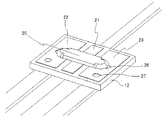
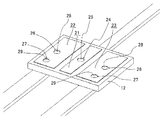
이하, 본 발명에 관한 제 1의 실시예에 관해, 도면을 참조하면서 상세히 기술한다. 본 발명에 관한 액셜 리드 타입의 보호 소자(10)는, 도 1에 그 표면측을 사시도로 도시하는 바와 같이, 세라믹 칩체(12)와, 이 표면측에 탑재한 실장 부품의 가용 합금 퓨즈 소자나 스루홀 내의 저항 발열 소자 등을 보호하는 패키지의 케이스 커버(14), 및 이면측의 패턴 전극에 접속된 도출 리드(15 내지 17)를 구비한다. 여기서, 세라믹 칩체(12)의 양면에는 패턴 전극이 형성되어 있고, 표면측에서 가용 합금 퓨즈 소자, 이면측에서 도출용 리드, 칩체 스루홀에 저항 발열 소자가 각각 실장된다. 도 2는 패키지의 케이스 커버(14)의 장착 전의 상태로 사시도를 도시하고, 세라믹 칩체(12)에 마련한 패턴 전극(21 내지 23) 상에, 플럭스를 표면에 피착한 가용 합금 퓨즈 소자(20)가 배치되고, 그 양단이 패턴 전극(22 및 23)과 솔더링되고, 중간점은 패턴 전극(21) 경유로 저항 발열 소자(도시 생략)에 접속된다. 도 3은 도 2의 가용 합금 퓨즈 소자(20)의 실장 전의 상태의 사시도를 도시한다. 세라믹 칩체(12)의 표면측 중앙의 제 1 패턴 전극(21), 그 양측에 한 쌍의 제 2 패턴 전극(22, 23)과, 각 패턴 전극 위치에 형성된 제 1 스루홀(24), 한 쌍의 제 2 스루홀(26, 27)이 형성된다. 이 중, 스루홀(24)에는 저항 발열 소자(25)가, 스루홀(26, 27)에는 도전 소재(28, 29)가 매설 배치되어 있다. 또한, 도시하지 않지만, 이 칩체(12)의 이면측에 형성된 3개의 패턴 전극은, 표면측 패턴 전극(21 내지 23)과 대응하고 있고, 저항 발열 소자(25) 및 도전 소재(28, 29)와 전기적으로 접속되어 있다.EMBODIMENT OF THE INVENTION Hereinafter, the 1st Example which concerns on this invention is described in detail, referring drawings. The
한편, 이면측에 장착한 도출용 리드(15 내지 17)는 평각 구리선이고, 패턴 전극에 솔더링되어 있다. 세라믹 칩체(12)는, 소결 처리 전의 그린 시트의 단계에서 소정의 형상으로 되고, 소망하는 스루홀의 가공이 실시된다. 소결 처리 후에, 도전 패턴의 패턴 인쇄, 또한, 스루홀 내에 저항체의 충전 처리가 실시된다. 세라믹 칩체는 소정의 패턴 전극이나 저항체가, 동시에 다수가 일괄 형성되고, 소정의 가공 처리 공정 후에 분리 분할하여 개별 부품이 된다. 세라믹 칩체는 양호한 절연성을 유지하는 것이면 알루미나 이외의 절연재라도 좋고, 이 절연 기판의 각 면에 소정의 형상으로 패턴 전극이 형성된다. 예를 들면, 미리 정해진 위치의 2개의 스루홀에 도전체가 마련되고, 1개의 스루홀에 저항체를 개재시켜, 양면의 패턴 전극과 전기적으로 접속된다. 여기서 주목되는 것은 스루홀 내에 배치한 저항체는 표면측에 스페이스를 필요로 하지 않고 소형 박형화에 기여하는 외에 종래의 막저항체에 비하여 큰 체적을 얻을 수 있다. 따라서 내(耐) 전력을 크게 할 수 있는 외에, 막형상 저항체에서 필요한 소부(燒付)를 생략할 수 있고, 또한 외상(外傷)이 생기지 않는다. 취급상에서의 사고나 불량 발생도 없고 장기 안정화가 도모된다.On the other hand, the lead 15-17 for lead attached to the back surface side is a flat copper wire, and is soldered to the pattern electrode. The
[실시예 2][Example 2]
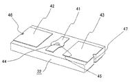
본 발명에 관한 다른 실시예는, 도 4의 사시도에 도시하는, 칩 타입의 보호 소자(30)이다. 도 4는 보호 커버를 제외한 표면측의 사시도를 도시하고 있고, 세라믹 칩체(32)의 표면에 가용 합금 퓨즈 소자(35)를 장착하여 구성되고, 표면 실장형 칩 부품으로서 취급하는 것이 가능한 구조이다. 이 칩 타입의 보호 소자(30)는, 세라믹 칩체(32)의 양면에 각각 중앙의 제 1 패턴 전극(41)과 단면(端面) 측에 제 2 패턴 전극(42, 43)이 형성되고, 이면측 패턴 전극이 그대로 프린트 기판상에 탑재되어 패턴 전극과의 사이가 솔더링 부착된다. 도 5는 보호 커버 및 가용 합금 퓨즈 소자의 장착 전의 상태를 도시하는 사시도이다. 도 5에는 세라믹 칩체(32)의 표면에 마련한 패턴 전극군이 도시되어 있고, 중앙에 제 1 패턴 전극(41), 단면측에 한 쌍의 제 2 패턴 전극(42, 43)이 형성되어 있다. 제 1 패턴 전극(41)에는 제 1 스루홀(44)이, 제 2 패턴 전극(42, 43)에는 기판 단면에 도전체 홈부(46, 47)가 각각 대응하도록 세라믹 칩체(32)에 형성된다. 여기서, 도 5에 도시되는 중앙 패턴 전극(41)에 대응하는 스루홀(44)에는 소정의 저항치로 조정된 저항 발열 소자(45)가 매설된다. 또한, 세라믹 칩체(32)의 전극 패턴(42 및 43)의 단면측에는 양면의 패턴 전극을 도통 접속하도록, 도전체 홈부(46, 47)가 형성되어 있다. 기판 중앙의 제 1 패턴 전극(41)도 양면에 형성되어 있고, 스루홀(44)에 마련한 저항 발열 소자(45)를 통하여 서로 전기적으로 접속된다.Another embodiment of the present invention is a chip
상술한 세라믹 칩체는, 가용 합금 퓨즈 소자, 저항 발열 소자 및 보호 커버를 탑재 실장하기 직전까지의 제작 공정을, 서로 다수의 연결 상태로 가공 처리된다. 즉, 복수 개의 세라믹 칩체는, 알루미나재 세라믹 칩이 연결된 상태로 일괄 처리에 의해 제조되고, 완성 직전의 공정에서, 개별화를 위해 분리 분할된다. 다수의 세라믹 칩을 연결 상태로 하여 가공 처리함으로써, 제품 사이의 편차를 작게 하는 외에, 제품 사이의 특성이나 성능의 균일화가 도모된다. 따라서 세라믹 칩체의 단면에의 도전체 홈부(46, 47)의 형성도, 다수의 칩 연합체에 형성된 스루홀에 도전 소재를 매설한 후에. 스루홀로 분리 절단하여 행하여진다. 도 4에 도시하는 바와 같이, 세라믹 칩체(32)의 표면측에 저융점 가용 합금에 플럭스를 피복한 가용 합금 퓨즈 소자(35)가, 그 양단을 패턴 전극과 솔더링되어 배치된다. 마찬가지로 하여, 양단면의 도전체 홈부(46, 47)를 경유하여 이면측 패턴 전극에 전기적으로 접속되고, 이들의 이면측의 패턴 전극에는 도출 단자를 솔더링하여 마련할 수도 있고, 이 도출 단자를 경유하여 표면 실장용 배선 기판과 전기적 회로를 구성한다. 가용 합금 퓨즈 소자(35)를 필요에 응하여 세라믹 캡이나 절연 피복재에 의해 밀봉하여, 패키지를 구성할 수도 있다. 여기서, 세라믹 칩체(32)의 스루홀(44)에 매입된 저항체의 발열 소자(45)는 세라믹 칩체(32)와 일체 배치되어 열적 결합 상태가 유지되기 때문에, 저항체의 발열은 직접 세라믹 칩체로부터 가용 합금 퓨즈 소자에 전열되고, 그에 의해, 신속하면서 정확하게 소정의 동작 온도로 작동시킬 수 있다. 여기서 각 구성 요소는 가급적 작으면서 얇아지도록 형성 가공된다. 예를 들면, 스루홀의 직경(φ)은, 예를 들면, 0.2㎜로 형성된다. 또한, 발열 소자의 저항치는 스루홀(44)의 표리 양면의 전극 패턴 사이에서 소망하는 저항치, 예를 들면, 내지 100Ω이 되도록 저항 재료나 스루홀 치수 등이 조정된다.The above-mentioned ceramic chip body is processed into a plurality of connected states with each other in the manufacturing process until just before mounting a fusible alloy fuse element, a resistance heating element, and a protective cover. That is, the plurality of ceramic chip bodies are manufactured by batch processing in the state where the alumina-based ceramic chips are connected, and are separated and separated for individualization in the process immediately before completion. By processing a plurality of ceramic chips in a connected state, the variation between products is reduced, and the characteristics and performance between the products can be equalized. Therefore, the formation of the
상술한 실시예에 있어서, 세라믹 칩체의 표리 양면에는 3개의 패턴 전극이 각각의 스루홀을 통하여 서로 접속되고, 이 중 하나의 스루홀에 저항 발열 소자를 매설 배치하였다. 표면측의 3개의 패턴 전극에는 가용 합금 퓨즈 소자가 다리를 놓는 형상으로 가교(架橋)되어 3개의 패턴 전극과 용착되고, 그에 의해, 저융점 합금의 제 1의 가용체 부분과 제 2의 가용체 부분을 갖는 듀얼 타입 가용 합금 퓨즈 소자가 된다. 각 패턴 전극에 용착된 저융점 합금의 가용체 부분에는 플럭스가 피착되어 가용 합금 퓨즈 소자가 된다. 필요에 따라, 패턴 전극을 포함하여 세라믹 칩체보다 약간 작은 절연성 세라믹 캡으로 밀폐 커버한다. 또한, 가용 합금 퓨즈 소자의 저융점 합금은 싱글 타입의 가용체라도 좋지만, 듀얼 타입의 가용체인 경우에는 각각의 가용체의 동작 온도를 동일하게 하거나 다른 것으로 할 수 있다. 다른 동작 온도의 듀얼 타입에서는 온도차를 동작 온도의 편차의 범위 내로 하는 것이 바람직하다.In the above-described embodiment, three pattern electrodes are connected to each other on both front and back sides of the ceramic chip body through respective through holes, and a resistive heating element is disposed in one of the through holes. The soluble alloy fuse element is bridge | crosslinked in the shape which bridge | crosslinks and welds with three pattern electrode to the three pattern electrodes of the surface side, and, thereby, the 1st soluble body part of a low melting-point alloy, and a 2nd soluble body It becomes a dual type soluble alloy fuse element having a portion. Flux is deposited on the soluble part of the low melting point alloy welded to each pattern electrode to form a soluble alloy fuse element. If necessary, the cover is covered with an insulating ceramic cap which is slightly smaller than the ceramic chip body, including the pattern electrode. The low melting point alloy of the soluble alloy fuse element may be a single type of soluble body, but in the case of a dual type of soluble body, the operating temperatures of the respective soluble bodies can be the same or different. In the dual type of other operating temperatures, it is preferable to keep the temperature difference within the range of the deviation of the operating temperature.
세라믹 칩체의 이면측에 형성한 3개의 패턴 전극에 도출용 리드나 도출 단자가 부착되어 피보호용 기기와 접속된다. 발열 소자는 제 1의 스루홀 내에 배치되어 있고, 제 1의 패턴 전극과 접속된다. 보호 소자는, 예를 들면, 규격 DC 32V, 10A, 동작 온도 135℃, 발열 저항 50Ω이고, 완성품의 외형 치수에 관해서는 세라믹 칩체 본체를 극히 작게 할 수 있다. 또한, 사각형 형상 세라믹 칩체(12)는 두께 0.4㎜의 알루미나 기판이고 소형화에 의해 알루미나 세라믹의 소요량이 대폭적으로 삭감되어 비용면에서의 경제적 메리트를 얻을 수 있음과 함께, 패턴 전극의 형성을 스크린 인쇄로 실시할 때에, 작은 기판이기 때문에 1회의 인쇄로 다수의 인쇄 가공이 동시에 가능한 등 제조상에서의 경제적 효과도 얻어진다. 또한, 리드 부재(15 내지 17)는 폭 0.7 내지 1.0㎜, 두께 0.2 내지 0.4㎜의 평판형상의 Sn 도금 구리선을 사용하였기 때문에 본체 부분의 두께 저감에 기여하여 박형화에 도움이 된다.Leading leads and lead terminals are attached to the three pattern electrodes formed on the rear surface side of the ceramic chip body and connected to the device to be protected. The heat generating element is disposed in the first through hole and is connected to the first pattern electrode. The protection element is, for example, a standard DC 32 V, 10 A, an operating temperature of 135 ° C., and a heat generating resistance of 50?, And the ceramic chip body can be made extremely small in terms of the external dimensions of the finished product. In addition, the rectangular
[실시예 3]Example 3
본 발명에 관한 보호 소자의 실장 구조는, 2차 전지의 과충전 보호 회로에의 적용이 가능하다. 메인 프린트 기판에 탑재되는 M0SFET 등의 능동 소자 사이에 세라믹 캡측을 아래에 하여 감입(嵌入)하도록 하여 부착된다. 상술한 바와 같이 세라믹 칩체의 한쪽의 면을 세라믹 캡의 패키지로 밀봉하는 보호 소자는, 이 부분을 능동 소자의 감열부에 근접하여 실장할 수 있다. 또한, 회로부품 소자 사이의 간극 공간을 이용하여 보호 소자를 실장함으로써, 소형 박형화에 유리해지고, 이런 종류의 보호 회로가 사용되는 컴팩트한 휴대용 정보 통신기기에 적합한 것이 된다. 또한, 2개 이상의 저항 발열체를 사용하는 경우에, 세라믹 칩체의 스루홀 내에 병렬적으로 배치함으로써, 가용 합금 퓨즈 소자에 대한 균일한 열전달을 달성하여 정밀도 향상을 도모할 수 있다. 또한, 부품의 소형화에 의해, 실장 상, 보호 회로의 제어 소자 사이의 스페이스를 유효 이용하여 보호 장치 전체의 컴팩트화에 도움이 되는 등의 효과를 이룬다.The mounting structure of the protection element which concerns on this invention is applicable to the overcharge protection circuit of a secondary battery. Between the active elements, such as the M0SFET mounted on the main printed circuit board, the ceramic cap side is attached to the bottom side so as to be indented. As described above, the protective element for sealing one surface of the ceramic chip body with the package of the ceramic cap can be mounted close to the heat-sensitive portion of the active element. In addition, by mounting the protection element by using the gap space between the circuit component elements, it is advantageous for miniaturization and it becomes suitable for the compact portable information communication apparatus in which this kind of protection circuit is used. In the case where two or more resistive heating elements are used, by arranging them in parallel in the through-holes of the ceramic chip body, it is possible to achieve uniform heat transfer to the soluble alloy fuse element and to improve accuracy. In addition, by miniaturization of the components, the space between the control elements of the protection circuit can be effectively used on the mounting, thereby achieving an effect of making the entire protection device compact.
금회 개시된 실시의 형태 및 실시예는 모든 점에서 예시이고, 제한적인 것이 아니라고 생각되어야 할 것이다. 본 발명의 범위는 상기한 설명이 아니라 특허청구의 범위에 의해 나타나고, 특허청구의 범위와 균등한 의미, 및 범위 내에서의 모든 변경이 포함되는 것이 의도된다.The embodiments and examples disclosed herein are to be considered in all respects only as illustrative and not restrictive. The scope of the present invention is shown by above-described not description but Claim, and it is intended that the meaning of a claim and equality and all the changes within a range are included.
10, 30 : 보호 소자
12, 32 : 세라믹 칩체
14 : 케이스 커버(캡)
15, 16, 17 : 도출 리드
20, 35 : 가용 합금 퓨즈 소자
21, 41 : 제 1 패턴 전극
22, 23, 42, 43 : 제 2 패턴 전극
24, 44 : 제 1 스루홀
25, 45 : 저항 발열 소자(칩 저항)
26, 27 : 제 2 스루홀
28, 29 : 도전 소재
46, 47 : 단면측 도전체 홈부10, 30: protection element
12, 32: ceramic chip body
14 case cover (cap)
15, 16, 17: lead drawn
20, 35: available alloy fuse element
21, 41: first pattern electrode
22, 23, 42, 43: second pattern electrode
24, 44: First through hole
25, 45: resistance heating element (chip resistance)
26, 27: second through hole
28, 29: conductive material
46, 47: cross section side conductor groove
Claims (7)
상기 가용 합금 퓨즈 소자는 적어도 2개 이상의 가용 부분으로 이루어지고, 각각의 가용 부분의 용단하는 온도를 동일 또는 다른 온도로 선정한 것을 특징으로 하는 보호 소자.The method of claim 1,
The soluble alloy fuse element is composed of at least two or more soluble portions, the protection element, characterized in that the melting temperature of each of the soluble portion selected at the same or different temperature.
상기 발열 소자는 제 1 스루홀에 매설 배치되고, 저항 재료의 선정에 의해 저항치가 조정된 칩 저항이고, 상기 세라믹 칩체의 표면측의 상기 가용 합금 퓨즈 소자와 이면측의 상기 패턴 전극의 도출 단자에 접속한 것을 특징으로 하는 보호 소자.3. The method according to claim 1 or 2,
The heat generating element is a chip resistor disposed in the first through hole, the resistance of which is adjusted by selection of a resistance material, and is provided to the lead terminals of the fusible alloy fuse element on the front side of the ceramic chip body and the pattern electrode on the back side. The protection element characterized by the above-mentioned.
상기 도출 단자는 동일 방향으로 늘어나는 평각형상 리드 도체에 접속되고, 배선 기판 평탄면에 따라 솔더 접속하는 것을 특징으로 하는 보호 소자.The method of claim 3, wherein
The lead-out terminal is connected to a flat lead conductor extending in the same direction, and is connected to a solder along the flat surface of the wiring board.
상기 발열 소자에 통하는 전류는 전지 팩용 충방전 제어 회로의 이상을 검지하는 제어 소자에 의해 생성되는 과충방전 방지에 이용되는 것을 특징으로 하는 보호 장치.6. The method of claim 5,
The current passing through the heat generating element is used for preventing overcharge and discharge generated by a control element that detects an abnormality in the charge / discharge control circuit for a battery pack.
단면(端面) 스루홀의 도통은, 스루홀의 단연부(端緣部)에 마련한 외층 표면 도체로 형성하는 것을 특징으로 하는 보호 장치.6. The method of claim 5,
The conduction of a cross-sectional through hole is formed by the outer layer surface conductor provided in the edge part of a through hole, The protection apparatus characterized by the above-mentioned.
Applications Claiming Priority (2)
| Application Number | Priority Date | Filing Date | Title |
|---|---|---|---|
| JPJP-P-2009-178918 | 2009-07-31 | ||
| JP2009178918A JP5305523B2 (en) | 2009-07-31 | 2009-07-31 | Protective element |
Publications (1)
| Publication Number | Publication Date |
|---|---|
| KR20110053896A true KR20110053896A (en) | 2011-05-24 |
Family
ID=43746000
Family Applications (1)
| Application Number | Title | Priority Date | Filing Date |
|---|---|---|---|
| KR1020100070764A KR20110053896A (en) | 2009-07-31 | 2010-07-22 | Protection element |
Country Status (4)
| Country | Link |
|---|---|
| JP (1) | JP5305523B2 (en) |
| KR (1) | KR20110053896A (en) |
| CN (1) | CN101989519B (en) |
| TW (1) | TWI485739B (en) |
Cited By (1)
| Publication number | Priority date | Publication date | Assignee | Title |
|---|---|---|---|---|
| KR20150082254A (en) * | 2012-11-07 | 2015-07-15 | 엔이씨 쇼트 컴포넌츠 가부시키가이샤 | Flux for protection elements, fuse element for protection elements, and circuit protection element |
Families Citing this family (9)
| Publication number | Priority date | Publication date | Assignee | Title |
|---|---|---|---|---|
| KR101266822B1 (en) | 2011-09-07 | 2013-05-23 | (주)엠에스테크비젼 | Platlike repeatable fuse |
| CN102522263A (en) * | 2011-12-31 | 2012-06-27 | 上海长园维安电子线路保护有限公司 | Temperature fuse capable of being soldered through reflow |
| JP5896412B2 (en) | 2012-05-17 | 2016-03-30 | エヌイーシー ショット コンポーネンツ株式会社 | Fuse element for protection element and circuit protection element using the same |
| CN103236380B (en) * | 2013-04-10 | 2015-07-01 | 南京萨特科技发展有限公司 | Over-current over-voltage protective element and manufacture method thereof |
| JP6151550B2 (en) * | 2013-04-25 | 2017-06-21 | デクセリアルズ株式会社 | Protective element |
| TWI680482B (en) * | 2014-01-15 | 2019-12-21 | 日商迪睿合股份有限公司 | Protection element |
| JP6480742B2 (en) * | 2015-02-05 | 2019-03-13 | 内橋エステック株式会社 | Protective element |
| CN106410762A (en) * | 2015-07-28 | 2017-02-15 | 有量科技股份有限公司 | Battery charging protection system and active fusing type protection device |
| JP6708387B2 (en) * | 2015-10-07 | 2020-06-10 | デクセリアルズ株式会社 | Switch element, electronic parts, battery system |
Family Cites Families (5)
| Publication number | Priority date | Publication date | Assignee | Title |
|---|---|---|---|---|
| JPH117877A (en) * | 1997-06-14 | 1999-01-12 | Uchihashi Estec Co Ltd | Alloy temperature fuse |
| JP2002033035A (en) * | 2000-07-18 | 2002-01-31 | Nec Schott Components Corp | Protection element |
| JP2003217416A (en) * | 2002-01-25 | 2003-07-31 | Nec Schott Components Corp | Temperature fuse and protective device mounted with the same |
| JP4110967B2 (en) * | 2002-12-27 | 2008-07-02 | ソニーケミカル&インフォメーションデバイス株式会社 | Protective element |
| JP2006221919A (en) * | 2005-02-09 | 2006-08-24 | Uchihashi Estec Co Ltd | Fuse with substrate type resistor and battery pack |
-
2009
- 2009-07-31 JP JP2009178918A patent/JP5305523B2/en active Active
-
2010
- 2010-07-01 TW TW099121642A patent/TWI485739B/en active
- 2010-07-22 KR KR1020100070764A patent/KR20110053896A/en not_active Application Discontinuation
- 2010-07-28 CN CN201010245159.1A patent/CN101989519B/en active Active
Cited By (1)
| Publication number | Priority date | Publication date | Assignee | Title |
|---|---|---|---|---|
| KR20150082254A (en) * | 2012-11-07 | 2015-07-15 | 엔이씨 쇼트 컴포넌츠 가부시키가이샤 | Flux for protection elements, fuse element for protection elements, and circuit protection element |
Also Published As
| Publication number | Publication date |
|---|---|
| JP5305523B2 (en) | 2013-10-02 |
| JP2011034755A (en) | 2011-02-17 |
| TWI485739B (en) | 2015-05-21 |
| CN101989519B (en) | 2014-08-06 |
| TW201110180A (en) | 2011-03-16 |
| CN101989519A (en) | 2011-03-23 |
Similar Documents
| Publication | Publication Date | Title |
|---|---|---|
| KR20110053896A (en) | Protection element | |
| TWI398894B (en) | Protection element | |
| US8767368B2 (en) | Protective element and method for producing the same | |
| KR101598778B1 (en) | Protection element and secondary battery device | |
| KR101256658B1 (en) | Surface mountable pptc device with integral weld plate | |
| KR100820535B1 (en) | Protection circuit-equipped secondary battery | |
| KR102523229B1 (en) | Protection element and mounted body | |
| TWI389159B (en) | Protection element | |
| KR20050099523A (en) | Protection element | |
| JP6017603B2 (en) | Composite protective element | |
| CN109074988B (en) | Protective element | |
| CN108701570B (en) | Thermal metal oxide varistor circuit protection device | |
| JP6707377B2 (en) | Protective element | |
| KR102481793B1 (en) | Thermal Fuse and Printed Circuit Board with Thermal Fuse | |
| JP4573865B2 (en) | Protective device using temperature fuse | |
| WO2017163766A1 (en) | Protection element | |
| CN110957188A (en) | Disconnecting element and disconnecting element circuit | |
| JP2003217416A (en) | Temperature fuse and protective device mounted with the same | |
| JP5546406B2 (en) | Ceramic fuse and ceramic fuse substrate | |
| JP6711704B2 (en) | Protective device with bypass electrode | |
| KR20090019697A (en) | Temperature fuse with resistance and an electric cell protection circuit board | |
| WO2020166445A1 (en) | Circuit module | |
| KR101504132B1 (en) | The complex protection device of blocking the abnormal state of current and voltage | |
| US9870886B2 (en) | Protective element and protective circuit substrate using the same | |
| KR101508098B1 (en) | The complex protection device of blocking the abnormal state of current and voltage |
Legal Events
| Date | Code | Title | Description |
|---|---|---|---|
| E902 | Notification of reason for refusal | ||
| E601 | Decision to refuse application |