KR20100070731A - 할로실리케이트 형광체, 이를 포함하는 백색 발광 소자 - Google Patents
할로실리케이트 형광체, 이를 포함하는 백색 발광 소자 Download PDFInfo
- Publication number
- KR20100070731A KR20100070731A KR1020080129410A KR20080129410A KR20100070731A KR 20100070731 A KR20100070731 A KR 20100070731A KR 1020080129410 A KR1020080129410 A KR 1020080129410A KR 20080129410 A KR20080129410 A KR 20080129410A KR 20100070731 A KR20100070731 A KR 20100070731A
- Authority
- KR
- South Korea
- Prior art keywords
- phosphor
- light emitting
- white light
- emitting device
- halosilicate
- Prior art date
Links
Images


Classifications
-
- C—CHEMISTRY; METALLURGY
- C09—DYES; PAINTS; POLISHES; NATURAL RESINS; ADHESIVES; COMPOSITIONS NOT OTHERWISE PROVIDED FOR; APPLICATIONS OF MATERIALS NOT OTHERWISE PROVIDED FOR
- C09K—MATERIALS FOR MISCELLANEOUS APPLICATIONS, NOT PROVIDED FOR ELSEWHERE
- C09K11/00—Luminescent, e.g. electroluminescent, chemiluminescent materials
- C09K11/08—Luminescent, e.g. electroluminescent, chemiluminescent materials containing inorganic luminescent materials
- C09K11/0883—Arsenides; Nitrides; Phosphides
-
- C—CHEMISTRY; METALLURGY
- C09—DYES; PAINTS; POLISHES; NATURAL RESINS; ADHESIVES; COMPOSITIONS NOT OTHERWISE PROVIDED FOR; APPLICATIONS OF MATERIALS NOT OTHERWISE PROVIDED FOR
- C09K—MATERIALS FOR MISCELLANEOUS APPLICATIONS, NOT PROVIDED FOR ELSEWHERE
- C09K11/00—Luminescent, e.g. electroluminescent, chemiluminescent materials
- C09K11/08—Luminescent, e.g. electroluminescent, chemiluminescent materials containing inorganic luminescent materials
- C09K11/59—Luminescent, e.g. electroluminescent, chemiluminescent materials containing inorganic luminescent materials containing silicon
-
- C—CHEMISTRY; METALLURGY
- C09—DYES; PAINTS; POLISHES; NATURAL RESINS; ADHESIVES; COMPOSITIONS NOT OTHERWISE PROVIDED FOR; APPLICATIONS OF MATERIALS NOT OTHERWISE PROVIDED FOR
- C09K—MATERIALS FOR MISCELLANEOUS APPLICATIONS, NOT PROVIDED FOR ELSEWHERE
- C09K11/00—Luminescent, e.g. electroluminescent, chemiluminescent materials
- C09K11/08—Luminescent, e.g. electroluminescent, chemiluminescent materials containing inorganic luminescent materials
- C09K11/66—Luminescent, e.g. electroluminescent, chemiluminescent materials containing inorganic luminescent materials containing germanium, tin or lead
-
- C—CHEMISTRY; METALLURGY
- C09—DYES; PAINTS; POLISHES; NATURAL RESINS; ADHESIVES; COMPOSITIONS NOT OTHERWISE PROVIDED FOR; APPLICATIONS OF MATERIALS NOT OTHERWISE PROVIDED FOR
- C09K—MATERIALS FOR MISCELLANEOUS APPLICATIONS, NOT PROVIDED FOR ELSEWHERE
- C09K11/00—Luminescent, e.g. electroluminescent, chemiluminescent materials
- C09K11/08—Luminescent, e.g. electroluminescent, chemiluminescent materials containing inorganic luminescent materials
- C09K11/77—Luminescent, e.g. electroluminescent, chemiluminescent materials containing inorganic luminescent materials containing rare earth metals
- C09K11/7728—Luminescent, e.g. electroluminescent, chemiluminescent materials containing inorganic luminescent materials containing rare earth metals containing europium
- C09K11/77342—Silicates
-
- C—CHEMISTRY; METALLURGY
- C09—DYES; PAINTS; POLISHES; NATURAL RESINS; ADHESIVES; COMPOSITIONS NOT OTHERWISE PROVIDED FOR; APPLICATIONS OF MATERIALS NOT OTHERWISE PROVIDED FOR
- C09K—MATERIALS FOR MISCELLANEOUS APPLICATIONS, NOT PROVIDED FOR ELSEWHERE
- C09K11/00—Luminescent, e.g. electroluminescent, chemiluminescent materials
- C09K11/08—Luminescent, e.g. electroluminescent, chemiluminescent materials containing inorganic luminescent materials
- C09K11/77—Luminescent, e.g. electroluminescent, chemiluminescent materials containing inorganic luminescent materials containing rare earth metals
- C09K11/7728—Luminescent, e.g. electroluminescent, chemiluminescent materials containing inorganic luminescent materials containing rare earth metals containing europium
- C09K11/7737—Phosphates
- C09K11/7738—Phosphates with alkaline earth metals
- C09K11/7739—Phosphates with alkaline earth metals with halogens
-
- C—CHEMISTRY; METALLURGY
- C09—DYES; PAINTS; POLISHES; NATURAL RESINS; ADHESIVES; COMPOSITIONS NOT OTHERWISE PROVIDED FOR; APPLICATIONS OF MATERIALS NOT OTHERWISE PROVIDED FOR
- C09K—MATERIALS FOR MISCELLANEOUS APPLICATIONS, NOT PROVIDED FOR ELSEWHERE
- C09K11/00—Luminescent, e.g. electroluminescent, chemiluminescent materials
- C09K11/08—Luminescent, e.g. electroluminescent, chemiluminescent materials containing inorganic luminescent materials
- C09K11/77—Luminescent, e.g. electroluminescent, chemiluminescent materials containing inorganic luminescent materials containing rare earth metals
- C09K11/7728—Luminescent, e.g. electroluminescent, chemiluminescent materials containing inorganic luminescent materials containing rare earth metals containing europium
- C09K11/774—Borates
-
- C—CHEMISTRY; METALLURGY
- C09—DYES; PAINTS; POLISHES; NATURAL RESINS; ADHESIVES; COMPOSITIONS NOT OTHERWISE PROVIDED FOR; APPLICATIONS OF MATERIALS NOT OTHERWISE PROVIDED FOR
- C09K—MATERIALS FOR MISCELLANEOUS APPLICATIONS, NOT PROVIDED FOR ELSEWHERE
- C09K11/00—Luminescent, e.g. electroluminescent, chemiluminescent materials
- C09K11/08—Luminescent, e.g. electroluminescent, chemiluminescent materials containing inorganic luminescent materials
- C09K11/77—Luminescent, e.g. electroluminescent, chemiluminescent materials containing inorganic luminescent materials containing rare earth metals
- C09K11/7766—Luminescent, e.g. electroluminescent, chemiluminescent materials containing inorganic luminescent materials containing rare earth metals containing two or more rare earth metals
- C09K11/7781—Sulfates
-
- C—CHEMISTRY; METALLURGY
- C09—DYES; PAINTS; POLISHES; NATURAL RESINS; ADHESIVES; COMPOSITIONS NOT OTHERWISE PROVIDED FOR; APPLICATIONS OF MATERIALS NOT OTHERWISE PROVIDED FOR
- C09K—MATERIALS FOR MISCELLANEOUS APPLICATIONS, NOT PROVIDED FOR ELSEWHERE
- C09K11/00—Luminescent, e.g. electroluminescent, chemiluminescent materials
- C09K11/08—Luminescent, e.g. electroluminescent, chemiluminescent materials containing inorganic luminescent materials
- C09K11/77—Luminescent, e.g. electroluminescent, chemiluminescent materials containing inorganic luminescent materials containing rare earth metals
- C09K11/7783—Luminescent, e.g. electroluminescent, chemiluminescent materials containing inorganic luminescent materials containing rare earth metals containing two or more rare earth metals one of which being europium
- C09K11/7784—Chalcogenides
- C09K11/7787—Oxides
-
- H—ELECTRICITY
- H01—ELECTRIC ELEMENTS
- H01L—SEMICONDUCTOR DEVICES NOT COVERED BY CLASS H10
- H01L33/00—Semiconductor devices with at least one potential-jump barrier or surface barrier specially adapted for light emission; Processes or apparatus specially adapted for the manufacture or treatment thereof or of parts thereof; Details thereof
- H01L33/48—Semiconductor devices with at least one potential-jump barrier or surface barrier specially adapted for light emission; Processes or apparatus specially adapted for the manufacture or treatment thereof or of parts thereof; Details thereof characterised by the semiconductor body packages
- H01L33/50—Wavelength conversion elements
- H01L33/501—Wavelength conversion elements characterised by the materials, e.g. binder
- H01L33/502—Wavelength conversion materials
- H01L33/504—Elements with two or more wavelength conversion materials
-
- H—ELECTRICITY
- H01—ELECTRIC ELEMENTS
- H01L—SEMICONDUCTOR DEVICES NOT COVERED BY CLASS H10
- H01L2224/00—Indexing scheme for arrangements for connecting or disconnecting semiconductor or solid-state bodies and methods related thereto as covered by H01L24/00
- H01L2224/01—Means for bonding being attached to, or being formed on, the surface to be connected, e.g. chip-to-package, die-attach, "first-level" interconnects; Manufacturing methods related thereto
- H01L2224/42—Wire connectors; Manufacturing methods related thereto
- H01L2224/44—Structure, shape, material or disposition of the wire connectors prior to the connecting process
- H01L2224/45—Structure, shape, material or disposition of the wire connectors prior to the connecting process of an individual wire connector
- H01L2224/45001—Core members of the connector
- H01L2224/45099—Material
- H01L2224/451—Material with a principal constituent of the material being a metal or a metalloid, e.g. boron (B), silicon (Si), germanium (Ge), arsenic (As), antimony (Sb), tellurium (Te) and polonium (Po), and alloys thereof
- H01L2224/45138—Material with a principal constituent of the material being a metal or a metalloid, e.g. boron (B), silicon (Si), germanium (Ge), arsenic (As), antimony (Sb), tellurium (Te) and polonium (Po), and alloys thereof the principal constituent melting at a temperature of greater than or equal to 950°C and less than 1550°C
- H01L2224/45144—Gold (Au) as principal constituent
-
- H—ELECTRICITY
- H01—ELECTRIC ELEMENTS
- H01L—SEMICONDUCTOR DEVICES NOT COVERED BY CLASS H10
- H01L2224/00—Indexing scheme for arrangements for connecting or disconnecting semiconductor or solid-state bodies and methods related thereto as covered by H01L24/00
- H01L2224/01—Means for bonding being attached to, or being formed on, the surface to be connected, e.g. chip-to-package, die-attach, "first-level" interconnects; Manufacturing methods related thereto
- H01L2224/42—Wire connectors; Manufacturing methods related thereto
- H01L2224/47—Structure, shape, material or disposition of the wire connectors after the connecting process
- H01L2224/48—Structure, shape, material or disposition of the wire connectors after the connecting process of an individual wire connector
- H01L2224/4805—Shape
- H01L2224/4809—Loop shape
- H01L2224/48091—Arched
-
- H—ELECTRICITY
- H01—ELECTRIC ELEMENTS
- H01L—SEMICONDUCTOR DEVICES NOT COVERED BY CLASS H10
- H01L2224/00—Indexing scheme for arrangements for connecting or disconnecting semiconductor or solid-state bodies and methods related thereto as covered by H01L24/00
- H01L2224/01—Means for bonding being attached to, or being formed on, the surface to be connected, e.g. chip-to-package, die-attach, "first-level" interconnects; Manufacturing methods related thereto
- H01L2224/42—Wire connectors; Manufacturing methods related thereto
- H01L2224/47—Structure, shape, material or disposition of the wire connectors after the connecting process
- H01L2224/48—Structure, shape, material or disposition of the wire connectors after the connecting process of an individual wire connector
- H01L2224/481—Disposition
- H01L2224/48151—Connecting between a semiconductor or solid-state body and an item not being a semiconductor or solid-state body, e.g. chip-to-substrate, chip-to-passive
- H01L2224/48221—Connecting between a semiconductor or solid-state body and an item not being a semiconductor or solid-state body, e.g. chip-to-substrate, chip-to-passive the body and the item being stacked
- H01L2224/48245—Connecting between a semiconductor or solid-state body and an item not being a semiconductor or solid-state body, e.g. chip-to-substrate, chip-to-passive the body and the item being stacked the item being metallic
- H01L2224/48247—Connecting between a semiconductor or solid-state body and an item not being a semiconductor or solid-state body, e.g. chip-to-substrate, chip-to-passive the body and the item being stacked the item being metallic connecting the wire to a bond pad of the item
-
- H—ELECTRICITY
- H01—ELECTRIC ELEMENTS
- H01L—SEMICONDUCTOR DEVICES NOT COVERED BY CLASS H10
- H01L2224/00—Indexing scheme for arrangements for connecting or disconnecting semiconductor or solid-state bodies and methods related thereto as covered by H01L24/00
- H01L2224/01—Means for bonding being attached to, or being formed on, the surface to be connected, e.g. chip-to-package, die-attach, "first-level" interconnects; Manufacturing methods related thereto
- H01L2224/42—Wire connectors; Manufacturing methods related thereto
- H01L2224/47—Structure, shape, material or disposition of the wire connectors after the connecting process
- H01L2224/48—Structure, shape, material or disposition of the wire connectors after the connecting process of an individual wire connector
- H01L2224/481—Disposition
- H01L2224/48151—Connecting between a semiconductor or solid-state body and an item not being a semiconductor or solid-state body, e.g. chip-to-substrate, chip-to-passive
- H01L2224/48221—Connecting between a semiconductor or solid-state body and an item not being a semiconductor or solid-state body, e.g. chip-to-substrate, chip-to-passive the body and the item being stacked
- H01L2224/48245—Connecting between a semiconductor or solid-state body and an item not being a semiconductor or solid-state body, e.g. chip-to-substrate, chip-to-passive the body and the item being stacked the item being metallic
- H01L2224/48257—Connecting between a semiconductor or solid-state body and an item not being a semiconductor or solid-state body, e.g. chip-to-substrate, chip-to-passive the body and the item being stacked the item being metallic connecting the wire to a die pad of the item
-
- H—ELECTRICITY
- H01—ELECTRIC ELEMENTS
- H01L—SEMICONDUCTOR DEVICES NOT COVERED BY CLASS H10
- H01L2224/00—Indexing scheme for arrangements for connecting or disconnecting semiconductor or solid-state bodies and methods related thereto as covered by H01L24/00
- H01L2224/01—Means for bonding being attached to, or being formed on, the surface to be connected, e.g. chip-to-package, die-attach, "first-level" interconnects; Manufacturing methods related thereto
- H01L2224/42—Wire connectors; Manufacturing methods related thereto
- H01L2224/47—Structure, shape, material or disposition of the wire connectors after the connecting process
- H01L2224/49—Structure, shape, material or disposition of the wire connectors after the connecting process of a plurality of wire connectors
- H01L2224/491—Disposition
- H01L2224/49105—Connecting at different heights
- H01L2224/49107—Connecting at different heights on the semiconductor or solid-state body
-
- H—ELECTRICITY
- H01—ELECTRIC ELEMENTS
- H01L—SEMICONDUCTOR DEVICES NOT COVERED BY CLASS H10
- H01L2224/00—Indexing scheme for arrangements for connecting or disconnecting semiconductor or solid-state bodies and methods related thereto as covered by H01L24/00
- H01L2224/73—Means for bonding being of different types provided for in two or more of groups H01L2224/10, H01L2224/18, H01L2224/26, H01L2224/34, H01L2224/42, H01L2224/50, H01L2224/63, H01L2224/71
- H01L2224/732—Location after the connecting process
- H01L2224/73251—Location after the connecting process on different surfaces
- H01L2224/73265—Layer and wire connectors
-
- Y—GENERAL TAGGING OF NEW TECHNOLOGICAL DEVELOPMENTS; GENERAL TAGGING OF CROSS-SECTIONAL TECHNOLOGIES SPANNING OVER SEVERAL SECTIONS OF THE IPC; TECHNICAL SUBJECTS COVERED BY FORMER USPC CROSS-REFERENCE ART COLLECTIONS [XRACs] AND DIGESTS
- Y02—TECHNOLOGIES OR APPLICATIONS FOR MITIGATION OR ADAPTATION AGAINST CLIMATE CHANGE
- Y02B—CLIMATE CHANGE MITIGATION TECHNOLOGIES RELATED TO BUILDINGS, e.g. HOUSING, HOUSE APPLIANCES OR RELATED END-USER APPLICATIONS
- Y02B20/00—Energy efficient lighting technologies, e.g. halogen lamps or gas discharge lamps
Abstract
넓은 반가폭을 갖는 할로실리케이트 형광체 및 이 형광체를 포함하는 백색 발광 소자가 제공되며, 이러한 백색 발광 소자는 연색성이 우수하다.
할로실리케이트 형광체, 백색 발광 소자
Description
할로실리케이트 형광체 및 이를 포함하는 백색 발광 소자가 개시된다. 보다 상세하게는 넓은 반가폭을 갖는 할로실리케이트 형광체 및 이를 포함하는 백색 발광 소자가 제공된다.
종래 광 시스템으로 형광등 및 백열등이 널리 사용된다. 그러나, 형광등에서 사용되는 Hg은 환경 문제를 야기한다. 또한, 상기 종래 광 시스템들은 수명이 매우 짧을 뿐 아니라, 그 효율도 매우 낮기 때문에 절전 측면에서 바람직하지 못하다. 이에 대하여 최근 많은 연구에 의해 백색 발광 소자의 효율이 증대되었다.
이러한 백색 발광 소자를 구현하는 방법은, UV LED를 광원으로 이용하고 빛의 삼원색인 삼원색 형광체를 여기시켜 백색을 구현하는 방식, 청색 LED를 광원으로 사용하여 적색 및 녹색 형광체를 여기시켜 백색을 구현하는 방식, 또는 청색 LED를 광원으로 사용하여 황색 형광체를 여기시킴으로써 백색을 구현하는 방식으로 구분된다.
상기 세 가지 방법 중에서 청색 LED를 광원으로 사용하여 황색 형광체를 여 기시킴으로써 백색을 구현하는 방식은 청색 LED에 황색 형광체로 Y3Al5O12:Ce3+, Tb3Al5O12:Ce3+, (Sr,Ba)2SiO4:Eu2+ 등을 결합하여 백색광을 만들어 내는 방식이 주종을 이루고 있다. 특히 Y3Al5O12:Ce3+의 경우 우수한 효율, 폭넓은 발광 밴드 등과 같은 특성으로 백색 LED용으로서 가장 적합한 형광체로 알려지고 있으나, 적색 영역의 발광이 부족하여 연색성이 낮고 차가운 느낌의 백색광 밖에 만들어 내지 못하는 단점을 가지고 있다.
또한, 오렌지색-황색 형광체로서 실리케이트계 형광체가 개발되었는데, 이를 청색 LED 광원으로 여기하여 백색광을 구현하는 백색 발광 소자가 알려져 있다.
본 발명의 한 측면은 넓은 반가폭을 갖는 할로실리케이트 형광체를 제공하는 것이다.
본 발명의 다른 측면은 상기 할로실리케이트 형광체의 제조 방법을 제공하는 것이다.
본 발명의 또 다른 측면은 상기 할로실리케이트 형광체를 포함하는 연색성이 우수한 백색 발광 소자를 제공하는 것이다.
본 발명의 한 측면에 따라 하기 화학식 1의 할로실리케이트 형광체가 제공된다:
상기 식에서
M1은 Sr2+ 및 Ba2+ 중에서 선택되는 적어도 1개이고,
M2는 Si4+ 및 Ge4+ 중에서 선택되는 적어도 1개이고,
M3는 Ca2+, Sr2+ 및 Ba2+ 중에서 선택되는 적어도 1개이고,
M4는 Eu2+, Mn2+, Sb2+,Ce3+, Pr3+, Nd3+, Sm3+, Tb3+, Dy3+, Ho3+, Er3+, Yb3+ 및 Bi3+ 중에서 선택되는 적어도 1개이고,
A는 F-, Cl-, Br- 및 I- 중에서 선택되는 적어도 1개이고,
0≤x<1,
1.8≤p≤2.2, 0.8≤q≤1.2, 1<r/q<3 및 0<s<0.5이다.
상기 할로실리케이트 형광체의 발광 스펙트럼의 반가폭은 125 내지 220nm일 수 있다.
본 발명의 다른 측면에 따라 발광 다이오드 (LED: light emitting diode); 및 상기 할로실리케이트 형광체를 포함하는 백색 발광 소자가 제공된다.
상기 백색 발광 소자에서 상기 발광 다이오드는 청색 발광 다이오드 또는 UV광 다이오드일 수 있다.
상기 백색 발광 소자에서 상기 할로실리케이트 형광체의 방출 스펙트럼의 피크 파장이 520 내지 670 nm일 수 있다.
상기 백색 발광 소자에서 청색 형광체, 녹색 형광체 및 적색 형광체 중에서 선택된 하나 이상을 더 포함할 수 있다.
상기 백색 발광 소자에서 상기 청색 형광체는 (Sr,Ba,Ca)5(PO4)3Cl:Eu2+; BaMg2Al16O27:Eu2+; Sr4Al14O25:Eu2+; BaAl8O13:Eu2+; BaMgAl10O17:Eu2+ 및 Sr2Si3O8(2SrCl2:Eu2+; Ba3MgSi2O8:Eu2+ 및 (Sr,Ca)10(PO4)6(nB2O3:Eu2+ 로 이루어진 군으 로부터 선택된 하나 이상일 수 있다.
상기 백색 발광 소자에서 상기 녹색 형광체는 (Ba,Sr,Ca)2SiO4:Eu2+; Ba2MgSi2O7:Eu2+; Ba2ZnSi2O7:Eu2+; BaAl2O4:Eu2+; SrAl2O4:Eu2+; BaMgAl10O17:Eu2+, Mn2+ ; 및 BaMg2Al16O27:Eu2+, Mn2+로 이루어진 군으로부터 선택된 하나 이상일 수 있다.
상기 백색 발광 소자에서 상기 적색 형광체는 (Ba,Sr,Ca)2Si5N8:Eu2+; (Sr,Ca)AlSiN3:Eu2+; Y2O3:Eu3+,Bi3+; (Ca,Sr)S:Eu2+; CaLa2S4:Ce3+; (Sr,Ca,Ba)2P2O7:Eu2+,Mn2+; (Ca,Sr)10(PO4)6(F,Cl):Eu2+,Mn2+; (Y,Lu)2WO6:Eu3+,Mo6+; (Gd,Y,Lu,La)2O3:Eu3+,Bi3+; (Gd,Y,Lu,La)2O2S:Eu3+,Bi3+; (Gd,Y,Lu,La)BO3:Eu3+,Bi3+; (Gd,Y,Lu,La)(P,V)O4:Eu3+,Bi3+ 및 (Ba,Sr,Ca)MgP2O7:Eu2+,Mn2+로 이루어진 군으로부터 선택된 하나 이상일 수 있다.
상기 백색 발광 소자에서 상기 할로실리케이트 형광체의 방출 스펙트럼 피크 파장이 520 내지 670 nm 일 수 있다.
상기 백색 발광 소자는 신호등, 통신 기기의 광원, 디스플레이 장치의 백라이트 또는 조명용일 수 있다.
본 발명의 한 측면에 따르면 반가폭이 넓은 할로실리케이트 형광체를 제공할 수 있고, 이를 포함하는 백색 발광 소자는 연색성이 뛰어나다.
이하, 본 발명의 일 구현예에 따른 할로실리케이트 형광체 및 이를 포함하는 백색 발광 소자에 대해 상세하게 설명하기로 한다.
본 발명의 한 측면에 따르면 하기 화학식 1의 할로실리케이트 형광체가 제공된다:
[화학식 1]
p(Ca1-xM1 x)O·qM2O2·rM3A2: sM4
상기 식에서
M1은 Sr2+ 및 Ba2+ 중에서 선택되는 적어도 1개이고,
M2는 Si4+ 및 Ge4+ 중에서 선택되는 적어도 1개이고,
M3는 Ca2+, Sr2+ 및 Ba2+ 중에서 선택되는 적어도 1개이고,
M4는 Eu2+, Mn2+, Sb2+,Ce3+, Pr3+, Nd3+, Sm3+, Tb3+, Dy3+, Ho3+, Er3+, Yb3+ 및 Bi3+ 중에서 선택되는 적어도 1개이고,
A는 F-, Cl-, Br-, 및 I- 중에서 선택되는 적어도 1개이고,
0≤x<1,
1.8≤p≤2.2, 0.8≤q≤1.2, 1<r/q<3 및 0<s<0.5이다.
상기 화학식 1에서 ·은 본 발명에서 청구하는 형광체를 구현하기 위하여 반응하는 금속 산화물과 금속 할로겐화물의 조합을 의미한다.
상기 할로실리케이트 형광체는 금속 이온의 조성에 따라, 약 360 nm 내지 약 470 nm 파장의 빛을 흡수하여 약 520 nm 내지 약 670 nm 피크 파장의 가시광을 발광할 수 있다. 따라서, 상기 할로실리케이트 형광체는 녹색에서 오렌지색에 이르는 넓은 범위에 걸쳐서 우수한 발광을 얻을 수 있는 물질이다. 특히, 종래의 Y3Al5O12:Ce3+나 Sr2SiO4:Eu2+ 보다 한참 넓은 약 125 내지 220 nm에 이르는 매우 넓은 반가폭을 보이며, 단독으로 또는 소량의 추가 형광체와 함께 청색 발광 다이오드에 적용하거나, 청색, 녹색 및 적색의 추가 형광체와 함께 UV 발광 다이오드에 적용하여, 우수한 연색성 및 색재현성을 갖는 백색 발광 소자를 구현할 수 있다. 이처럼 폭 넓은 대역의 발광이 가능한 것은 상기 할로실리케이트 형광체가 2 이상의 상(phase) 이 혼합되어 있는 것에서 기인한다. 즉 Ca, Sr 및 Ba 중 1종 이상의 할로겐화물과 Si 및 Ge 중 1종 이상의 산화물의 혼합비인 r/q의 값에 따라 구성하는 각각의 상에서 발광하는 빛의 상대 강도가 바뀌어 전체적인 발광 톤이 바뀌게 되는데, r/q이 증가할수록 황색 발광에서 녹색 발광의 기여가 커지며, r/q가 감소할수록 오렌지색 발광의 기여가 커진다. 특히, 빛의 시감도(luminosity factor)와 연색성을 고려할 때 1<r/q<3 구간에서 청색 발광 다이오드와 결합하여 백색광을 만들 수 있는 양질의 황색 형광체를 구현할 수 있다.
상기 할로실리케이트 형광체는 a) Ca 산화물 단독, 또는 Sr 산화물과 Ba 산화물 중 1종 이상과의 혼합물; b) Si 산화물 단독 또는 Ge 산화물과의 혼합물; 및 c) Eu 산화물 단독 또는 Mn, Sb,Ce, Pr, Nd, Sm, Tb, Dy, Ho, Er, Yb, 및 Bi로 이루어지는 군으로부터 선택된 1종 이상의 금속의 산화물과의 혼합물의 반응물; 및 d) Ca, Sr 또는 Ba의 할로겐화물로부터 제조될 수 있다.
상기 a), b), c) 및 d) 성분의 사용량은 화학식 1에서의 p, q, r 및 s가 정해진 범위내에 들도록 선택하면 된다.
Ca 산화물을 Sr 산화물과 Ba 산화물 중 1 종 이상과 혼합하여 사용하는 경우 이들 간의 혼합비는 몰 비로 (Sr+Ba):Ca가 0.0001:1 내지 2:3일 수 있다.
또한 Si 산화물을 Ge 산화물과 혼합하여 사용하는 경우 이들 간의 혼합비는 몰 비로 Ge:Si가 0.0001:1 내지 1:3일 수 있다.
또한 Eu 산화물을 Mn, Sb, Ce, Pr, Nd, Sm, Tb, Dy, Ho, Er, Yb 및 Bi로 이루어지는 군으로부터 선택된 1종 이상의 금속의 산화물과 혼합하여 사용하는 경우 이들 간의 혼합비는 몰 비로 A:Eu (A= Mn, Sb, Ce, Pr, Nd, Sm, Tb, Dy, Ho, Er, Yb 및 Bi로 이루어지는 군으로부터 선택된 1종 이상의 금속)가 0.0001:1 내지 9:1일 수 있다.
상기 반응 물질에서 산화물로 표시한 것은 출발 물질로 탄산염, 질산염, 수산화물 또는 아세트산염 등의 어떤 것을 사용하더라도 고온 합성시 산화되어 결국 산화물로 바뀌기 때문이다. 따라서 출발물질은 산화물의 몰 비가 상기 범위 내에 든다면 금속의 산화물 뿐 아니라 탄산염, 질산염, 수산화물, 아세트산염 등 다른 형태의 것도 가능하다. 상기 할로실리케이트 형광체의 출발 물질중 Ca, Sr 또는 Ba의 할로겐화물은 2상 이상으로 이루어지는 형광체의 구성 원소로서 기능할 뿐만 아니라, 녹는점이 800˚C 이하로써 1000˚C 부근의 공정 온도에서 결정성을 높이는 플럭스로서의 역할을 하여, 종래와 같은 플럭스로 사용될 물질을 추가할 필요 없이 고품질의 결정이 합성되도록 하는 장점을 지닌다.
상기 백색 발광 소자는 높은 연색 지수 (Color Rendering Index)를 갖는 백색광을 구현할 수 있어 의료용, 식료품 전시용, 박물관, 미술관 등에서 필수 불가결하며 고품질 생활 조명으로 적용 가능하다.
상기 본 발명의 일 측면에 따른 할로실리케이트 형광체의 제조 방법은 특별히 제한되지는 않고, 공지된 기술 즉, 고상법, 액상법 또는 기상법 중 어느 것에 의하여 제조될 수 있다.
예를 들어 고상법에 의할 경우, Ca 산화물 (단독 또는 Sr 산화물과 Ba 산화물 중 1종 이상과의 혼합물); Si 산화물(단독 또는 Ge 산화물과의 혼합물); Eu 산화물(단독 또는 Mn, Sb, Ce, Pr, Nd, Sm, Tb, Dy, Ho, Er, Yb, 및 Bi로 이루어지는 군으로부터 선택된 1종 이상의 금속의 산화물과의 혼합물); 및 Ca, Sr 또는 Ba의 할로겐화물의 혼합 분말을 준비한 다음, 이를 약 500℃ 내지 1000℃에서 1 시간 내지 10 시간 동안 대기하에서 1차 소성한 후, 다시 1차 소성 결과물을 수소와 질소의 혼합 가스의 환원 분위기 하에서 약 700℃ 내지 1200℃에서 2차 소결한다. 여기에서 상기 혼합 가스에서 수소의 함량은 적어도 5 부피% 정도가 되도록 조절한다.
상기 Eu 산화물 단독 또는 Mn, Sb, Ce, Pr, Nd, Sm, Tb, Dy, Ho, Er, Yb, 및 Bi로 이루어지는 군으로부터 선택된 1종 이상의 금속의 산화물과의 혼합물은 열처리 시 형광체 결정 내부에 이온으로 도핑되어 할로실리케이트 형광체가 발광할 때 부활제(activator)로 작용한다.
상기 소결을 2 단계에 걸쳐 실시하는 것은 1차 소결은 혼합 원료에 포함된 수분, 유기물 또는 일부염의 착화합물과 같은 불순물을 제거시키면서 결정 성장을 촉진시키는 위함이다. 만약 1차 소결온도가 500℃ 미만이면 결정이 잘 형성되지 않고, 1000℃를 초과하면 혼합 원료의 승화가 일어나 화학양론비가 깨지거나, 혼합 성분내에서 불필요한 미반응 물질을 형성할 수 있어 오히려 최종적인 형광체의 결정성을 떨어 뜨려 형광체의 파장 변환 효율을 저하시킬 수 있다.
상기 2차 소결온도가 700℃ 미만이면 합성 반응이 원활하게 이루어지지 못해서 원하는 발광 세기를 얻을 수 없게 되고, 1200℃를 초과하면 목적물이 고온에서 용해되어 유리상이 형성되어 발광 세기가 감소하며 원하는 물성의 분말을 얻기가 어려울 수 있다.
이렇게 얻은 소결체를 분말로 분쇄하고, 증류수로 세척하여, 원하는 형광체를 얻을 수 있다.
본 발명의 또 다른 측면에 따르면 발광 다이오드(LED: light emitting diode); 및 상기 할로실리케이트 형광체를 포함하는 백색 발광 소자가 제공된다.
상기 백색 발광 소자에서, 상기 발광 다이오드는 청색 또는 UV LED일 수 있으며, 여기 광원의 피크 파장 대역이 360 내지 470nm 범위일 수 있다.
상기 백색 발광 소자에서, 상기 할로실리케이트 형광체의 방출 스펙트럼의 피크 파장은 520 내지 670 nm일 수 있다.
상기 백색 발광 소자는 청색 형광체 , 녹색 형광체 및 적색 형광체 중에서 선택된 하나 이상을 더 포함할 수 있다.
상기 청색 형광체의 예를 들면, (Sr,Ba,Ca)5(PO4)3Cl:Eu2+; BaMg2Al16O27:Eu2+; Sr4Al14O25:Eu2+; BaAl8O13:Eu2+; BaMgAl10O17:Eu2+ 및 Sr2Si3O8·(2SrCl2:Eu2+; Ba3MgSi2O8:Eu2+; (Sr,Ca)10(PO4)6(nB2O3:Eu2+ 등을 들 수 있으며, 이들을 하나 이상 혼합하여 포함할 수 있다.
상기 녹색 형광체의 예를 들면, (Ba,Sr,Ca)2SiO4:Eu2+; Ba2MgSi2O7:Eu2+; Ba2ZnSi2O7:Eu2+; BaAl2O4:Eu2+; SrAl2O4:Eu2+; BaMgAl10O17:Eu2+, Mn2+ ; 및 BaMg2Al16O27:Eu2+,Mn2+ 등을 들 수 있으며, 이들을 하나 이상 혼합하여 포함할 수 있다.
상기 적색 형광체의 예를 들면, (Ba,Sr,Ca)2Si5N8:Eu2+; (Sr,Ca)AlSiN3:Eu2+; Y2O3:Eu3+,Bi3+; (Ca,Sr)S:Eu2+; CaLa2S4:Ce3+; (Sr,Ca,Ba)2P2O7:Eu2+,Mn2+; (Ca,Sr)10(PO4)6(F,Cl):Eu2+,Mn2+; (Y,Lu)2WO6:Eu3+,Mo6+; (Gd,Y,Lu,La)2O3:Eu3+,Bi3+; (Gd,Y,Lu,La)2O2S:Eu3+,Bi3+; (Gd,Y,Lu,La)BO3:Eu3+,Bi3+; (Gd,Y,Lu,La)(P,V)O4:Eu3+,Bi3+ 및 (Ba,Sr,Ca)MgP2O7:Eu2+,Mn2+로 이루어진 군으로부터 선택된 하나 이상일 수 있다.
도 1은 본 발명의 일 구현예에 따른 백색 발광 소자의 구조를 나타낸 개략도로서, 고분자 렌즈 타입의 표면실장형 백색 발광 소자를 도시한 것이다. 여기에서 고분자 렌즈의 일 실시예로서 에폭시 렌즈를 사용한다.
도 1을 참조하여, UV LED 칩(10)은 금 와이어(20)를 통하여 전기 리드선(30)과 다이 본딩되고, 본 발명의 일 측면에 따른 할로실리케이트 형광체를 함유하는 형광체 조성물(40)을 포함하도록 에폭시 몰드층(50)이 형성되어 있다. 그리고 도 1에서 성형몰드(60)의 내부는 알루미늄 또는 은으로 코팅된 반사막으로 이루어지며, 이는 다이오드에서 방출된 광을 위로 반사시키는 역할 및 적당량의 에폭시를 가두는 역할을 한다.
상기 에폭시 몰드층(50) 상부에는 에폭시 돔 렌즈(70)가 형성되어 있고, 이 에폭시 돔 렌즈(70)는 원하는 지향각에 따라 모양이 변화될 수 있다.
본 발명의 한 측면에 따른 백색 발광 소자는 도 1의 구조로만 한정되는 것을 의미하는 것은 아니며, 이밖에 다른 구조 예를 들어 백색 발광 소자에 형광체가 실장되는 타입, 포탄형, PCB 타입의 표면 실장형 타입의 구조를 갖는 백색 발광 소자 일 수 있다.
본 발명의 일 측면에 따른 할로실리케이트 형광체는 상술한 백색 발광 소자 외에 수은 램프, 크세논 램프 등과 같은 램프 또는 자발광 액정 표시 소자에도 적용 가능하다.
이하, 본 발명의 구현예를 하기 실시예를 들어 상세히 설명하기로 하되, 발명의 범위가 하기 실시예로만 한정되는 것은 아니다.
실시예 1
2CaO·SiO2·1.2CaCl2:0.025Eu2+
고상 반응법을 사용하여 제조하였다. 즉 원료 분말 CaCO3 6.66 g, SiO2 2 g, 및 Eu2O3 0.30g을 막자 사발을 이용하여 30분 동안 혼합하였다. 혼합된 분말을 알루미나 반응 용기에 담고 대기하 1000˚C에서 5시간 동안 열처리하여 Ca2SiO4:Eu2+ 5.73g를 얻었다. 상기 Ca2SiO4:Eu2+ 5.73g과 CaCl2·2H2O 5.87g을 막자 사발을 이용하여 30분 가량 혼합하고 최종적으로 H2/N2=5/95 분위기 1000˚C에서 8시간 동안 소성하였다. 소성이 끝난 샘플을 막자 사발에서 분쇄하고 상온의 증류수로 분말을 세정하여 형광체 분말을 얻었다. 얻어진 형광체의 발광스펙트럼에서 반가폭은 200nm이었다.
실시예 2
2CaO·SiO2·1.7CaCl2:0.025Eu2+
상기 실시예 1의 방법으로 Ca2SiO4:Eu2+ 5.73g를 얻었다. 상기 Ca2SiO4:Eu2+ 5.73g과 CaCl2·2H2O 8.7g을 막자 사발을 이용하여 30분 가량 혼합하고 최종적으로 H2/N2=5/95 분위기 1000˚C에서 8시간 동안 소성하였다. 소성이 끝난 샘플을 막자 사발에서 분쇄하고 상온의 증류수로 분말을 세정하여 형광체 분말을 얻었다. 얻어진 형광체의 발광스펙트럼에서 반가폭은 165nm이었다.
실시예 3
2CaO·SiO2·2.1CaCl2:0.025Eu2+
상기 실시예 1의 방법으로 Ca2SiO4:Eu2+ 5.73g를 얻었다. 상기 Ca2SiO4:Eu2+ 5.73g과 CaCl2·2H2O 10.7g을 막자 사발을 이용하여 30분 가량 혼합하고 최종적으로 H2/N2=5/95 분위기 1000˚C에서 8시간 동안 소성하였다. 소성이 끝난 샘플을 막자 사발에서 분쇄하고 상온의 증류수로 분말을 세정하여 형광체 분말을 얻었다. 얻어진 형광체의 발광스펙트럼에서 반가폭은 130nm이었다.
비교예 1
Ca3SiO4Cl2:Eu2+의 제조
고상 반응법을 사용하여 제조하였다. 즉 원료 분말 CaCO3 6.66 g, SiO2 2 g, CaCl2·2H2O 5.00g 및 Eu2O3 0.30g을 막자 사발을 이용하여 30분 동안 혼합하였다. 혼합된 분말을 알루미나 반응 용기에 H2/N2=5/95 분위기 1000˚C에서 8시간 동안 소성하였다. 소성이 끝난 샘플을 막자 사발에서 분쇄하고 상온의 증류수로 분말을 세정하여 형광체 분말을 얻었다. 얻어진 형광체의 발광스펙트럼에서 반가폭은 100nm이었다.
비교예 2
Y3Al5O12:Ce3+의 제조
고상 반응법을 사용하여 제조하였다. 즉 원료 분말 Y2O3 4.00 g, Al2O3 3.20 g 및 CeO2 0.34g 을 막자 사발을 이용하여 30분 동안 혼합하였다. 혼합된 분말을 알루미나 반응 용기에 H2/N2=5/95 분위기 1400˚C에서 6시간 동안 소성하였다. 소성이 끝난 샘플을 막자 사발에서 분쇄하고 상온의 증류수로 분말을 세정하여 형광체 분말을 얻었다. 얻어진 형광체의 발광스펙트럼에서 반가폭은 120nm이었다.
비교예 3
Sr2SiO4:Eu2+의 제조
고상 반응법을 사용하여 제조하였다. 즉 원료 분말 SrCO3 8.00 g, SiO2 1.65 g, 및 Eu2O3 0.12g을 막자 사발을 이용하여 30분 동안 혼합하였다. 혼합된 분말을 알루미나 반응 용기에 H2/N2=5/95 분위기 1300˚C에서 6시간 동안 소성하였다. 소성이 끝난 샘플을 막자 사발에서 분쇄하고 상온의 증류수로 분말을 세정하여 형광체 분말을 얻었다. 얻어진 형광체의 발광스펙트럼에서 반가폭은 100nm이었다.
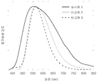
도 2 내지 도 4는 각각 실시예 1 내지 실시예 3에서 제조한 형광체의 400 nm에서 여기된 발광 스펙트럼을 도시한 것이다. 도 5는 실시예 1 및 비교예 2와 비교예 3에서 제조된 형광체의 발광 스펙트럼을 도시한 것이다. 이 도면으로부터 본 발명의 일 구현예에 따른 형광체의 반가폭이 훨씬 넓다는 것을 확인할 수 있다.
도 6은 실시예 1 및 비교예 2와 비교예 3에서 제조된 형광체의 색좌표를 나타낸 것이다. 이 도면들로부터 Y3Al5O12:Ce3+나 Sr2SiO4:Eu2+와 더불어 본 발명의 형광체 역시 청색 LED에 적용됨으로써 백색광을 얻을 수 있음을 확인할 수 있다.
도 7은 본 발명의 실시예 1 내지 3 및 비교예 1에 따른 형광체의 XRD 결과를 나타내는 그래프이다. 상기 도면으로부터 출발물질 중 CaCl2가 일정 범위내에서 그 함량이 증가함에 따라 비교예 1의 경우에는 나타나지 않은 새로운 피크의 상대 강도가 커짐을 확인할 수 있다. 따라서 본 발명의 구현예에 따른 할로실리케이트 형광체는 단일 상이 아닌 2상 이상의 혼합물임을 확인할 수 있다. r/q가 1.2에서 1.7, 2.1로 증가함에 따라, 공지의 Ca3SiO4Cl2 상에 비해 종래에 보고되지 않은 새로운 상(들)의 상대량이 증가하고 있다. 또한 도 2 내지 도 4의 발광 피크의 변화가 새로운 상의 증가에서 비롯되고 있음을 확인할 수 있다.
도 1은 본 발명의 일 구현예에 따른 백색 발광 소자의 구조를 나타낸 개략도이다.
도 2는 본 발명의 일 구현예에 따른 할로실리케이트 형광체의 400nm에서 여기한 발광 스펙트럼을 도시한 것이다.
도 3은 본 발명의 다른 구현예에 따른 할로실리케이트 형광체의 400 nm에서 여기한 발광 스펙트럼을 도시한 것이다
도 4는 본 발명의 또 다른 구현예에 따른 할로실리케이트 형광체의 400 nm에서 여기한 발광 스펙트럼을 도시한 것이다.
도 5는 본 발명의 일 구현에에 따른 할로실리케이트 형광체와 종래의 형광체의 발광스펙트럼을 비교한 것이다.
도 6은 본 발명의 일 구현예에 따른 할로실리케이트 형광체와 종래의 형광체의 발광 스펙트럼과 청색 LED 스펙트럼의 색좌표상의 위치를 도시한 것이다.
도 7은 본 발명의 일 구현예에 따른 할로실리케이트 형광체 및 종래의 형광체의 XRD 그래프를 도시한 것이다.
<도면의 주요 부분에 대한 부호의 설명>
10: LED 칩 20: 금 와이어
30: 전기 리드선 40: 형광체 조성물
50: 에폭시 몰딩층 60: 성형 몰드
70: 에폭시 돔 렌즈
Claims (10)
- 하기 화학식 1의 할로실리케이트 형광체:[화학식 1]p(Ca1-xM1 x)O·qM2O2·rM3A2: sM4상기 식에서M1은 Sr2+ 및 Ba2+ 중에서 선택되는 적어도 1개이고,M2는 Si4+ 및 Ge4 + 중에서 선택되는 적어도 1개이고,M3는 Ca2+, Sr2+ 및 Ba2+ 중에서 선택되는 적어도 1개이고,M4는 Eu2+, Mn2+, Sb2+,Ce3+, Pr3+, Nd3+, Sm3+, Tb3+, Dy3+, Ho3+, Er3+, Yb3+ 및 Bi3+ 중에서 선택되는 적어도 1개이고,A는 F-, Cl-, Br-, 또는 I- 중에서 선택되는 적어도 1개이고,0≤x<1,1.8≤p≤2.2, 0.8≤q≤1.2, 1<r/q<3 및 0<s<0.5이다.
- 제1항에 있어서,상기 할로실리케이트 형광체의 발광 스펙트럼에서 반가폭이 125 내지 220nm 인 할로실리케이트 형광체.
- 발광 다이오드 (LED: light emitting diode); 및제1항에 따른 할로실리케이트 형광체를 포함하는 백색 발광 소자.
- 제3항에 있어서,상기 발광 다이오드가 청색 또는 UV 발광 다이오드인 백색 발광 소자.
- 제3항에 있어서,청색 형광체, 녹색 형광체 및 적색 형광체 중에서 선택된 하나 이상을 더 포함하는 백색 발광 소자.
- 제5항에 있어서,상기 청색 형광체는 (Sr,Ba,Ca)5(PO4)3Cl:Eu2+; BaMg2Al16O27:Eu2+; Sr4Al14O25:Eu2+; BaAl8O13:Eu2+; BaMgAl10O17:Eu2+ 및 Sr2Si3O8(2SrCl2:Eu2+; Ba3MgSi2O8:Eu2+ 및 (Sr,Ca)10(PO4)6(nB2O3:Eu2+ 로 이루어진 군으로부터 선택된 하나 이상인 백색 발광 소자.
- 제5항에 있어서,상기 녹색 형광체는 (Ba,Sr,Ca)2SiO4:Eu2+; Ba2MgSi2O7:Eu2+; Ba2ZnSi2O7:Eu2+; BaAl2O4:Eu2+; SrAl2O4:Eu2+; BaMgAl10O17:Eu2+, Mn2+ ; 및 BaMg2Al16O27:Eu2+, Mn2+로 이루어진 군으로부터 선택된 하나 이상인 백색 발광 소자.
- 제5항에 있어서,상기 적색 형광체는 (Ba,Sr,Ca)2Si5N8:Eu2+; (Sr,Ca)AlSiN3:Eu2+; Y2O3:Eu3+,Bi3+; (Ca,Sr)S:Eu2+; CaLa2S4:Ce3+; (Sr,Ca,Ba)2P2O7:Eu2+,Mn2+; (Ca,Sr)10(PO4)6(F,Cl):Eu2+,Mn2+; (Y,Lu)2WO6:Eu3+,Mo6+; (Gd,Y,Lu,La)2O3:Eu3+,Bi3+; (Gd,Y,Lu,La)2O2S:Eu3+,Bi3+; (Gd,Y,Lu,La)BO3:Eu3+,Bi3+; (Gd,Y,Lu,La)(P,V)O4:Eu3+,Bi3+; (Ba,Sr,Ca)MgP2O7:Eu2+,Mn2+ 로 이루어진 군으로부터 선택된 하나 이상인 백색 발광 소자.
- 제3항에 있어서,상기 할로실리케이트 형광체의 방출 스펙트럼 피크 파장이 520 내지 670 nm 인 백색 발광 소자.
- 제3항에 있어서,상기 백색 발광 소자는 신호등, 통신 기기의 광원, 디스플레이 장치의 백라이트 또는 조명용인 백색 발광 소자.
Priority Applications (3)
| Application Number | Priority Date | Filing Date | Title |
|---|---|---|---|
| KR1020080129410A KR20100070731A (ko) | 2008-12-18 | 2008-12-18 | 할로실리케이트 형광체, 이를 포함하는 백색 발광 소자 |
| US12/556,369 US8274210B2 (en) | 2008-12-18 | 2009-09-09 | Halosilicate phosphor and white light emitting device including the same |
| JP2009285376A JP2010144170A (ja) | 2008-12-18 | 2009-12-16 | ハロシリケート蛍光体、これを含む白色発光素子 |
Applications Claiming Priority (1)
| Application Number | Priority Date | Filing Date | Title |
|---|---|---|---|
| KR1020080129410A KR20100070731A (ko) | 2008-12-18 | 2008-12-18 | 할로실리케이트 형광체, 이를 포함하는 백색 발광 소자 |
Publications (1)
| Publication Number | Publication Date |
|---|---|
| KR20100070731A true KR20100070731A (ko) | 2010-06-28 |
Family
ID=42264985
Family Applications (1)
| Application Number | Title | Priority Date | Filing Date |
|---|---|---|---|
| KR1020080129410A KR20100070731A (ko) | 2008-12-18 | 2008-12-18 | 할로실리케이트 형광체, 이를 포함하는 백색 발광 소자 |
Country Status (3)
| Country | Link |
|---|---|
| US (1) | US8274210B2 (ko) |
| JP (1) | JP2010144170A (ko) |
| KR (1) | KR20100070731A (ko) |
Cited By (1)
| Publication number | Priority date | Publication date | Assignee | Title |
|---|---|---|---|---|
| WO2013058478A1 (ko) * | 2011-10-17 | 2013-04-25 | 한국과학기술원 | 산화물계 녹색 형광체 및 그의 제조방법 및 이를 이용한 백색 led |
Families Citing this family (6)
| Publication number | Priority date | Publication date | Assignee | Title |
|---|---|---|---|---|
| JP2013225373A (ja) * | 2010-08-18 | 2013-10-31 | Sharp Corp | 照明装置、表示装置、及びテレビ受信装置 |
| EP2717337B1 (en) * | 2011-06-03 | 2018-02-21 | Citizen Electronics Co., Ltd. | Semiconductor light-emitting device, exhibit irradiation illumination device, meat irradiation illumination device, vegetable irradiation illumination device, fresh fish irradiation illumination device, general-use illumination device, and semiconductor light-emitting system |
| TWI432555B (zh) | 2011-08-12 | 2014-04-01 | Unity Opto Technology Co Ltd | 鋁酸鹽類化合物螢光粉 |
| CN103343004A (zh) * | 2013-07-01 | 2013-10-09 | 彩虹集团公司 | 一种CaxSiO4Cly:Eu2+荧光粉及其制备方法 |
| CN104130774B (zh) * | 2014-08-15 | 2016-05-11 | 昆明学院 | 一种氯硅酸盐荧光粉及其制备方法 |
| CN106497565B (zh) * | 2016-10-21 | 2019-03-12 | 中国科学院长春应用化学研究所 | 一种Yb离子激活的近红外长余辉发光材料及其制备方法 |
Family Cites Families (20)
| Publication number | Priority date | Publication date | Assignee | Title |
|---|---|---|---|---|
| FR2432039B1 (ko) * | 1978-07-28 | 1981-08-14 | Rhone Poulenc Ind | |
| DE3863870D1 (de) * | 1987-08-17 | 1991-08-29 | Agfa Gevaert Nv | Reproduktion von roentgenbildern durch photoanregbaren phosphor. |
| US5034607A (en) * | 1989-02-07 | 1991-07-23 | Agfa-Gevaert, N.V. | Reproduction of X-ray images with photostimulable phosphor |
| CN1203557C (zh) | 2000-05-29 | 2005-05-25 | 电灯专利信托有限公司 | 基于发光二极管的发射白光的照明设备 |
| DE10026435A1 (de) * | 2000-05-29 | 2002-04-18 | Osram Opto Semiconductors Gmbh | Kalzium-Magnesium-Chlorosilikat-Leuchtstoff und seine Anwendung bei Lumineszenz-Konversions-LED |
| US7311858B2 (en) | 2004-08-04 | 2007-12-25 | Intematix Corporation | Silicate-based yellow-green phosphors |
| US8017035B2 (en) * | 2004-08-04 | 2011-09-13 | Intematix Corporation | Silicate-based yellow-green phosphors |
| DE102004038199A1 (de) | 2004-08-05 | 2006-03-16 | Patent-Treuhand-Gesellschaft für elektrische Glühlampen mbH | LED mit niedriger Farbtemperatur |
| JP4836429B2 (ja) * | 2004-10-18 | 2011-12-14 | 株式会社東芝 | 蛍光体およびこれを用いた発光装置 |
| JP2006219636A (ja) | 2005-02-14 | 2006-08-24 | Matsushita Electric Works Ltd | 蛍光体及びその製造方法、発光装置 |
| TW200644283A (en) | 2005-02-23 | 2006-12-16 | Sumitomo Chemical Co | Fluorescent substance and light-emitting apparatus and white light emitting diode |
| EP1889892B1 (en) | 2005-05-30 | 2010-11-03 | Nemoto & Co., Ltd. | Green light emitting phosphor |
| KR100672972B1 (ko) | 2005-07-01 | 2007-01-22 | 웨이 젠 슈 | 백색발광다이오드 |
| US8906262B2 (en) * | 2005-12-02 | 2014-12-09 | Lightscape Materials, Inc. | Metal silicate halide phosphors and LED lighting devices using the same |
| US20070145879A1 (en) * | 2005-12-22 | 2007-06-28 | Abramov Vladimir S | Light emitting halogen-silicate photophosphor compositions and systems |
| JP2007231250A (ja) | 2006-02-02 | 2007-09-13 | Nichia Chem Ind Ltd | 蛍光体及びそれを用いた発光装置 |
| JP2007217605A (ja) | 2006-02-17 | 2007-08-30 | Matsushita Electric Works Ltd | 蛍光体及びその製造方法、発光装置 |
| CN100590173C (zh) | 2006-03-24 | 2010-02-17 | 北京有色金属研究总院 | 一种荧光粉及其制造方法和所制成的电光源 |
| US7820075B2 (en) * | 2006-08-10 | 2010-10-26 | Intematix Corporation | Phosphor composition with self-adjusting chromaticity |
| EP2084242A4 (en) * | 2006-10-03 | 2009-12-16 | Sarnoff Corp | METAL SILICATE HALIDE PHOSPHORES AND LED LIGHTING DEVICES USING THE SAME |
-
2008
- 2008-12-18 KR KR1020080129410A patent/KR20100070731A/ko not_active Application Discontinuation
-
2009
- 2009-09-09 US US12/556,369 patent/US8274210B2/en not_active Expired - Fee Related
- 2009-12-16 JP JP2009285376A patent/JP2010144170A/ja not_active Ceased
Cited By (1)
| Publication number | Priority date | Publication date | Assignee | Title |
|---|---|---|---|---|
| WO2013058478A1 (ko) * | 2011-10-17 | 2013-04-25 | 한국과학기술원 | 산화물계 녹색 형광체 및 그의 제조방법 및 이를 이용한 백색 led |
Also Published As
| Publication number | Publication date |
|---|---|
| US20100156274A1 (en) | 2010-06-24 |
| US8274210B2 (en) | 2012-09-25 |
| JP2010144170A (ja) | 2010-07-01 |
Similar Documents
| Publication | Publication Date | Title |
|---|---|---|
| KR101399652B1 (ko) | 실리케이트 형광체, 이를 포함하는 백색 발광 소자 | |
| JP4457110B2 (ja) | 改善された演色性を有するledをベースとする高効率の照明系 | |
| EP1449264B1 (en) | Photoluminescent material for light emitting diodes, and light emitting diode | |
| US7811472B2 (en) | Phosphor composition and method for producing the same, and light-emitting device using the same | |
| EP1413619A1 (en) | Luminescent material, especially for LED application | |
| KR101390908B1 (ko) | (옥시)나이트라이드 형광체 및 이를 포함하는 백색 발광 소자 | |
| US20110248303A1 (en) | METHOD FOR PREPARING A B-SiAION PHOSPHOR | |
| KR20080096597A (ko) | 발광체 및 상기 발광체를 포함하는 광 소스, 및 상기 발광체를 형성하기 위한 방법 | |
| JP2005048105A (ja) | 蛍光体組成物およびそれを用いた発光装置 | |
| JP2007507096A (ja) | 定義された色温度を有する白色発光led | |
| JP2005336450A (ja) | 蛍光体組成物とその製造方法、並びにその蛍光体組成物を用いた発光装置 | |
| US8242680B2 (en) | Green phosphors, methods of preparing the green phosphors, and white light-emitting devices including the green phosphors | |
| KR20100070731A (ko) | 할로실리케이트 형광체, 이를 포함하는 백색 발광 소자 | |
| JP2006299168A (ja) | 蛍光体およびそれを用いた発光装置 | |
| KR100682876B1 (ko) | 실리코포스페이트계 형광체 및 이를 포함한 led | |
| JP5125039B2 (ja) | 希土類酸窒化物系蛍光体及びこれを用いた発光装置 | |
| KR20110050206A (ko) | 옥시나이트라이드 형광체, 그 제조 방법 및 그것을 사용한 백색 발광 소자 | |
| KR20110000286A (ko) | (옥시)나이트라이드 형광체의 제조방법, 이로부터 얻어진 (옥시)나이트라이드 형광체 및 이를 구비한 백색 발광 소자 | |
| JP2014019870A (ja) | 蛍光体及び発光装置 | |
| KR101176212B1 (ko) | 알카리 토류 포스포러스 나이트라이드계 형광체와 그 제조방법 및 이를 이용한 발광장치 | |
| JP5194395B2 (ja) | 酸窒化物系蛍光体及びこれを用いた発光装置 | |
| KR20110082837A (ko) | 나이트라이드 형광체, 그 제조 방법 및 그것을 사용한 백색 발광 소자 | |
| KR20090019730A (ko) | (옥시)나이트라이드 형광체, 이를 포함하는 백색 발광 소자및 형광체 제조 방법 | |
| KR100571882B1 (ko) | 황색 형광체 및 이를 포함하는 백색 발광 장치 | |
| JP2023057392A (ja) | 発光装置、照明装置、画像表示装置及び車両用表示灯 |
Legal Events
| Date | Code | Title | Description |
|---|---|---|---|
| A201 | Request for examination | ||
| E902 | Notification of reason for refusal | ||
| E601 | Decision to refuse application |