KR102434661B1 - A method for conveying a group of electronic components during pick and place process - Google Patents
A method for conveying a group of electronic components during pick and place process Download PDFInfo
- Publication number
- KR102434661B1 KR102434661B1 KR1020200063372A KR20200063372A KR102434661B1 KR 102434661 B1 KR102434661 B1 KR 102434661B1 KR 1020200063372 A KR1020200063372 A KR 1020200063372A KR 20200063372 A KR20200063372 A KR 20200063372A KR 102434661 B1 KR102434661 B1 KR 102434661B1
- Authority
- KR
- South Korea
- Prior art keywords
- axis
- group
- electronic components
- aligner
- nest
- Prior art date
Links
Images


Classifications
-
- H—ELECTRICITY
- H05—ELECTRIC TECHNIQUES NOT OTHERWISE PROVIDED FOR
- H05K—PRINTED CIRCUITS; CASINGS OR CONSTRUCTIONAL DETAILS OF ELECTRIC APPARATUS; MANUFACTURE OF ASSEMBLAGES OF ELECTRICAL COMPONENTS
- H05K13/00—Apparatus or processes specially adapted for manufacturing or adjusting assemblages of electric components
- H05K13/08—Monitoring manufacture of assemblages
- H05K13/081—Integration of optical monitoring devices in assembly lines; Processes using optical monitoring devices specially adapted for controlling devices or machines in assembly lines
- H05K13/0812—Integration of optical monitoring devices in assembly lines; Processes using optical monitoring devices specially adapted for controlling devices or machines in assembly lines the monitoring devices being integrated in the mounting machine, e.g. for monitoring components, leads, component placement
-
- H—ELECTRICITY
- H05—ELECTRIC TECHNIQUES NOT OTHERWISE PROVIDED FOR
- H05K—PRINTED CIRCUITS; CASINGS OR CONSTRUCTIONAL DETAILS OF ELECTRIC APPARATUS; MANUFACTURE OF ASSEMBLAGES OF ELECTRICAL COMPONENTS
- H05K13/00—Apparatus or processes specially adapted for manufacturing or adjusting assemblages of electric components
- H05K13/04—Mounting of components, e.g. of leadless components
- H05K13/0404—Pick-and-place heads or apparatus, e.g. with jaws
-
- H—ELECTRICITY
- H05—ELECTRIC TECHNIQUES NOT OTHERWISE PROVIDED FOR
- H05K—PRINTED CIRCUITS; CASINGS OR CONSTRUCTIONAL DETAILS OF ELECTRIC APPARATUS; MANUFACTURE OF ASSEMBLAGES OF ELECTRICAL COMPONENTS
- H05K13/00—Apparatus or processes specially adapted for manufacturing or adjusting assemblages of electric components
- H05K13/08—Monitoring manufacture of assemblages
- H05K13/081—Integration of optical monitoring devices in assembly lines; Processes using optical monitoring devices specially adapted for controlling devices or machines in assembly lines
- H05K13/0813—Controlling of single components prior to mounting, e.g. orientation, component geometry
Abstract
본 발명은 픽 앤 플레이스 공정 중에 전자 부품 그룹을 이송하기 위한 방법에 관한 것으로서, 이는 낮은 시간당 유닛(UPH) 문제를 극복하고 전자 부품(102) 변환 시간을 감소 또는 제거하여 공정을 개선하기 위하여 일회성 동작으로 수행되고, 이에 의해 상기 방법은 단일 픽 앤 플레이스 공정에서 칩 또는 다이와 같은 다수의 크기 또는 유형의 전자 부품(102)을 제공할 수 있다. The present invention relates to a method for transferring a group of electronic components during a pick and place process, which is a one-time operation to overcome the low unit per hour (UPH) problem and improve the process by reducing or eliminating the electronic component 102 conversion time. , whereby the method can provide electronic components 102 of multiple sizes or types, such as chips or dies, in a single pick and place process.
Description
본 발명은 픽 앤 플레이스 공정 동안 전자 부품 그룹을 이송하는 방법으로서, 이는 복수의 픽업 헤드를 갖는 픽 앤 플레이스 장치에 의해 상기 전자 부품 그룹을 특정 위치에 플레이스하는 단계로서, 상기 특정 위치는 적어도 4 개의 네스트 벽으로부터 각각 떨어지게 미리 결정된 XY 오프셋을 갖는 네스트인 단계; 상기 네스트 벽에 대하여, 상기 그룹 내의 각 전자 부품의 XY 위치를 결정하기 위해, 적어도 하나의 사전 정렬기 비전 검사 시스템에 의해 상기 전자 부품 그룹의 적어도 하나의 이미지를 캡처하는 단계; 상기 네스트 벽에 대하여, 상기 그룹내의 모든 전자 부품의 XY 위치가 미리 결정된 오프셋 값 내에 있으면, 적어도 하나의 정렬기 모듈이 상기 그룹내의 각각의 전자 부품을 서로에 대해 정렬시키는 단계; 상기 네스트 벽에 대하여, 상기 그룹내의 임의의 전자 부품의 XY 위치가 미리 결정된 오프셋 값 내에 있지 않으면, 적어도 하나의 픽업 메커니즘이 전자 부품의 상기 그룹을 픽업하여, 적어도 하나의 리젝트 빈으로 전달하거나, 또는 사용자는 상이한 미리 결정된 오프셋 값을 갖는 상기 그룹내에서의 영향 받은(affected, 떨어지게) 전자 부품를 재검사하는 단계를 포함한다. The present invention provides a method for transporting a group of electronic components during a pick and place process, comprising the steps of placing the group of electronic components at a specific location by a pick and place device having a plurality of pickup heads, wherein the specific location includes at least four nesting each having a predetermined XY offset away from the nest wall; capturing at least one image of the group of electronic components by at least one pre-aligner vision inspection system to determine an XY position of each electronic component within the group relative to the nest wall; aligning, by at least one aligner module, each electronic component in the group relative to each other, if the XY positions of all electronic components in the group with respect to the nest wall are within a predetermined offset value; if the XY position of any electronic component in the group with respect to the nest wall is not within a predetermined offset value, then at least one pickup mechanism picks up the group of electronic components and delivers them to the at least one reject bin; or the user retesting the affected electronic components within the group having different predetermined offset values.
종래의 픽 앤 플레이스 공정 및 소팅 공정은 다이 또는 개별화된 패키지와 같은 전자 부품이 픽 앤 플레이스 메커니즘에 의해 개별적으로 픽업 및 이송되어, 시간당 낮은 유닛(UPH) 문제를 야기하는 심각한 결점을 겪는 것으로 잘 알려져 있다. 또한, 상이한 크기 또는 유형의 전자 부품에 대한 변환 시간은 또한 낮은 처리량 공정을 야기시킨다.It is well known that the conventional pick-and-place process and sorting process suffers from serious drawbacks in that electronic components such as dies or individualized packages are individually picked up and transported by a pick-and-place mechanism, resulting in low units per hour (UPH) problems. have. In addition, conversion times for different sizes or types of electronic components also result in low throughput processes.
Cheng et al., US 7,190,446 B1은 반도체 패키지와 같은 전자 부품을 처리하기 위한 장치 및 방법을 개시하였다. 이 특허에 표시된 바와 같이, 개별화된 패키지는 테이프로부터 개별적으로 픽업되어, 회전 테이블의 특정 세그먼트에서 홀더 상에 플레이스된다. 온로딩 위치와 오프로딩 위치 사이의 제 1 광학 시스템은 홀더에 의해 지지되는 동안 전자 장치의 제 1 표면을 검사하도록 구성되고, 동시에 또는 후속하여, 온로딩 위치와 오프로딩 위치 사이의 제 2 광학 시스템은 홀더에 의해 지지되는 동안, 제 1 표면에 반대쪽인 전자 장치의 제 2 표면을 검사하도록 구성된다. 마지막으로, 패키지는 패키지를 다른 오프로딩 장치로 개별적으로 이송하는 오프로딩 아암에 의해 개별적으로 픽업되도록 세그먼트로 회전된다. 이 경우, 패키지를 개별적으로 픽업하여 이송하면, 공정 속도가 느려져서 시간당 낮은 유닛(UPH) 문제가 발생하고, 처리량이 낮은 공정로 이어진다. Cheng et al., US 7,190,446 B1 discloses an apparatus and method for processing electronic components such as semiconductor packages. As indicated in this patent, individualized packages are individually picked up from tape and placed on a holder in a specific segment of a turntable. The first optical system between the onloading position and the offloading position is configured to inspect a first surface of the electronic device while being supported by the holder, and simultaneously or subsequently, a second optical system between the onloading position and the offloading position and configured to inspect a second surface of the electronic device opposite the first surface while being supported by the silver holder. Finally, the packages are rotated into segments to be individually picked up by offloading arms that individually transport the packages to other offloading devices. In this case, picking up and transporting packages individually slows down the process, resulting in low units per hour (UPH) issues, leading to low throughput processes.
Na et al., US 6,446,354 B1에 개시된 바와 같이, 핸들러 시스템은 카세트에 증착된 스트립 중 적어도 하나를 로딩하기 위한 온-로더 유닛, 온-로더 유닛으로부터 스트립을 드로어 피커에 유지하기 위한 드로어 유닛, 피커 헤드를 유지한 후 흡입 방식으로 고정하고 스트립을 절단 장치로 이송하여 그것을 복수의 개별 패키지 장치로 절단하기 위한 스트립 이송 유닛, 흡입 진공력을 사용하여 개별 패키지 장치를 고정 및 유지한 후, 브러시 및 에어 노즐을 사용하여 개별 패키지 장치를 세정하기 위한 패키지 세정 유닛; 세정 후 개별 패키지 장치를 건조하기 위한 패키지 건조 유닛, 건조 후 이동 및 예치를 위한 패키지 예치 유닛, 품질 검사를 위해 개별 패키지 장치를 유지 및 배치하기 위한 패키지 픽업 유닛, 패키지 예치 유닛의 일측에 장착된 패키지 픽업 유닛, 개별 패키지 장치의 품질을 검사하기 위한 시각 검사 수단, 및 개별 패키지 장치를 패키지 예치 유닛에 안착시키기 위하여 흡입 진공력을 사용하여 개별 패키지 장치(C)를 유지하며 검사 결과에 기초하여 분류된 개별 패키지 장치가 포함되어 있는 트레이를 이송하기 위한 패키지 트레이 예치 유닛을 구비한다. 이 방법은 픽 헤드 디자인이 복잡하고 z-방향으로 개별 진공 패드를 구동하기 위해 여러 모터를 사용해야 하기 때문에 탐낼 수 있다.As disclosed in Na et al., US 6,446,354 B1, the handler system comprises an on-loader unit for loading at least one of the strips deposited on the cassette, a drawer unit for holding the strip from the on-loader unit to a drawer picker, a picker A strip conveying unit for holding the head and then fixing it in a suction way and transferring the strip to a cutting device to cut it into a plurality of individual packaging devices, using suction vacuum force to fix and hold the individual packaging devices, then brush and air a package cleaning unit for cleaning individual package devices using a nozzle; A package drying unit for drying the individual package device after cleaning, a package deposit unit for moving and depositing after drying, a package pickup unit for holding and placing the individual package device for quality inspection, a package mounted on one side of the package depositing unit A pickup unit, a visual inspection means for inspecting the quality of the individual package device, and a suction vacuum force to seat the individual package device on the package depositing unit are used to hold the individual package device (C) and are classified based on the inspection result. and a package tray depositing unit for transferring trays containing individual package devices. This method is coveted because the pick head design is complex and requires the use of multiple motors to drive individual vacuum pads in the z-direction.
따라서, 픽 앤 플레이스 공정 동안 전자 부품 그룹을 일회성 동작으로 이송하는 방법에 의해 낮은 시간당 유닛(UPH) 문제를 극복하고, 상기 방법은 단일 픽 앤 플레이스 공정에서 칩 또는 다이와 같은 다수의 크기 또는 유형의 전자 부품을 제공할 수 있기 때문에, 전자 부품 변환 시간을 감소 또는 제거하여 공정을 개선함으로써 상기 단점을 완화하는 것이 유리할 것이다. Thus, the low unit per hour (UPH) problem is overcome by a method of transferring a group of electronic components in a one-time operation during a pick and place process, said method comprising multiple sizes or types of electronic devices such as chips or dies in a single pick and place process. It would be advantageous to alleviate this disadvantage by improving the process by reducing or eliminating the electronic component conversion time, since components can be provided.
따라서, 본 발명의 주요 목적은 픽 앤 플레이스(pick and place) 공정 동안 전자 부품 그룹을 이송하는 방법을 제공하는 것으로서, 상기 방법이 상기 전자 부품을 일회성 동작으로 픽업함으로써 시간당 낮은 유닛(UPH) 문제를 극복하는 것을 목표로 한다.Accordingly, a primary object of the present invention is to provide a method for transferring a group of electronic components during a pick and place process, wherein the method overcomes the low unit per hour (UPH) problem by picking up the electronic components in a one-time operation. aim to overcome.
본 발명의 또 다른 목적은 픽 앤 플레이스 공정 동안 전자 부품 그룹을 이송하는 방법을 제공하는 것으로서, 상기 방법이 단일 픽 앤 플레이스 공정에서 다수의 크기 및 다수의 유형의 전자 부품을 제공할 수 있게 하는 것이다. It is another object of the present invention to provide a method for transferring a group of electronic components during a pick and place process, which method enables the provision of multiple sizes and types of electronic components in a single pick and place process. .
본 발명의 또 다른 목적은 픽 앤 플레이스 공정 동안 전자 부품 그룹을 이송하는 방법을 제공하는 것으로서, 상기 방법이 생산 스루풋을 향상시킬 수 있는 방법을 제공하는 것이다.Another object of the present invention is to provide a method for transferring a group of electronic components during a pick and place process, wherein the method can improve production throughput.
본 발명의 또 다른 목적은 픽 앤 플레이스 공정 동안 한 그룹의 전자 부품을 이송하는 방법을 제공하는 것으로서, 상기 방법이 상이한 크기 또는 다른 유형의 전자 부품에 대한 변환 시간을 감소시키거나 제거할 수 있게 하는 것이다.Another object of the present invention is to provide a method for transporting a group of electronic components during a pick and place process, which method allows to reduce or eliminate the conversion time for different size or different types of electronic components. will be.
본 발명의 다른 추가의 목적은 다음의 본 발명의 상세한 설명을 이해하거나 또는 본 발명을 실시할 때 명백해질 것이다.Other further objects of the present invention will become apparent when the following detailed description of the invention is understood or when the invention is practiced.
본 발명의 바람직한 실시 예에 따르면, 다음이 제공된다:According to a preferred embodiment of the present invention, there is provided:
픽 앤 플레이스 공정(1) 동안 전자 부품 그룹을 이송하는 방법으로서,A method for transferring a group of electronic components during a pick and place process (1), comprising:
(i) 복수의 픽업 헤드를 갖는 픽 앤 플레이스 장치에 의해 상기 전자 부품 그룹을 특정 위치에 플레이스하는 단계를 포함하는 방법에 있어서, 상기 특정 위치는 적어도 4 개의 네스트 벽으로부터 각각 떨어지게 미리 결정된 XY 오프셋을 갖는 네스트이고;(i) placing the group of electronic components at specific locations by a pick-and-place device having a plurality of pickup heads, wherein the specific locations have a predetermined XY offset each away from at least four nest walls. is a nest with;
상기 방법은 단계(i) 이후에, 다음의 단계들:The method comprises, after step (i), the following steps:
(ii) 상기 네스트 벽에 대하여, 상기 그룹 내의 각 전자 부품의 XY 위치를 결정하기 위해, 적어도 하나의 사전 정렬기 비전 검사 시스템에 의해 상기 전자 부품 그룹의 적어도 하나의 이미지를 캡처하는 단계;(ii) capturing at least one image of the group of electronic components by at least one pre-aligner vision inspection system to determine an XY position of each electronic component within the group with respect to the nest wall;
(iii) 상기 네스트 벽에 대하여, 상기 그룹내의 모든 전자 부품의 XY 위치가 미리 결정된 오프셋 값 내에 있으면, 적어도 하나의 정렬기 모듈이 상기 그룹내의 각각의 전자 부품을 서로에 대해 정렬시키는 단계;(iii) with respect to the nest wall, if the XY positions of all electronic components in the group are within a predetermined offset value, then at least one aligner module aligns each electronic component in the group with respect to each other;
(iv) 상기 네스트 벽에 대하여, 상기 그룹내의 임의의 전자 부품의 XY 위치가 미리 결정된 오프셋 값 내에 있지 않으면, 적어도 하나의 픽업 메커니즘이 전자 부품의 상기 그룹을 픽업하여, 적어도 하나의 리젝트 빈으로 전달하거나, 또는 사용자는 상이한 미리 결정된 오프셋 값을 갖는 상기 그룹내에서의 영향 받은 전자 부품을 재검사하는 단계;(iv) with respect to the nest wall, if the XY position of any electronic component in the group is not within a predetermined offset value, then at least one pickup mechanism picks up the group of electronic components to at least one reject bin. forwarding, or the user retesting the affected electronic components within the group having different predetermined offset values;
를 추가로 포함한다. further includes.
본 발명의 다른 측면 및 장점은 첨부 도면과 함께 상세한 설명을 연구한 후에 식별될 것이다 :
도 1은 본 발명의 예시적인 방법 흐름을 도시한다.
도 2a는 X-축 액추에이터를 갖는 본 발명의 예시적인 도면(정면도)을 도시한다.
도 2b는 Y-축 액추에이터를 갖는 본 발명의 예시적인 도면(측면도)을 도시한다.
도 3a는 픽 앤 플레이스 공정 동안 전자 부품 그룹을 정렬시키는 본 발명의 예시적인 방법을 도시한다.
도 3b는 픽 앤 플레이스 공정 동안 전자 부품 그룹을 정렬시키는 본 발명의 다른 예시적인 방법을 도시한다.
도 4a 및 도 4b는 픽 앤 플레이스 공정 동안 전자 부품 그룹을 정렬시키는 본 발명의 예시적인 도면을 도시한다.Other aspects and advantages of the present invention will become apparent after studying the detailed description in conjunction with the accompanying drawings:
1 shows an exemplary method flow of the present invention.
2A shows an exemplary view (front view) of the present invention with an X-axis actuator.
2B shows an exemplary view (side view) of the present invention with a Y-axis actuator.
3A illustrates an exemplary method of the present invention for aligning a group of electronic components during a pick and place process.
3B illustrates another exemplary method of the present invention for aligning a group of electronic components during a pick and place process.
4A and 4B show exemplary views of the present invention for aligning groups of electronic components during a pick and place process.
다음의 상세한 설명에서, 본 발명의 철저한 이해를 제공하기 위해 다수의 특정 세부 사항이 설명된다. 그러나, 당업자는 본 발명이 이러한 특정 세부 사항 없이도 실시될 수 있음을 이해할 것이다. 다른 경우에, 잘 알려진 방법, 절차 및/또는 구성 요소는 본 발명을 모호하게 하지 않기 위해 상세히 설명되지 않았다.In the following detailed description, numerous specific details are set forth in order to provide a thorough understanding of the present invention. However, it will be understood by one of ordinary skill in the art that the present invention may be practiced without these specific details. In other instances, well-known methods, procedures, and/or components have not been described in detail in order not to obscure the present invention.
본 발명은 실시 예에 대한 다음의 설명으로부터 더 명확하게 이해될 것이며, 이는 단지 일정한 비율로 도시되지 않은 첨부 도면을 참조하여 제공된 것이다.BRIEF DESCRIPTION OF THE DRAWINGS The present invention will be more clearly understood from the following description of embodiments, which are provided only with reference to the accompanying drawings, which are not drawn to scale.
본 명세서 및 첨부된 청구 범위에 사용된 바와 같이, 단수 형태 "a", "an" 및 "the"는 문맥 상 명백하게 다르게 지시되지 않는 한, 복수 지시 대상을 포함한다.As used in this specification and the appended claims, the singular forms “a”, “an” and “the” include plural referents unless the context clearly dictates otherwise.
본 명세서의 개시내용 및 청구 범위에서, "포함하고 있는" 및 "포함하는"과 같은 "포함하다" 및 그 변형은 "포함하지만 이에 제한되지 않는"을 의미하고, 예를 들어, 다른 구성 요소, 정수 또는 단계를 배제하도록 의도되지 않는다. "예시적인"은 "예"를 의미하고 바람직한 또는 이상적인 구체 예의 지시를 전달하도록 의도되지 않으며, "예를 들어"는 제한적인 의미로 사용되지 않고 설명 목적으로 사용된다.In the disclosure and claims herein, "comprises", such as "comprising" and "comprising", and variations thereof, mean "including, but not limited to," and include, for example, other elements; It is not intended to exclude integers or steps. “Exemplary” means “example” and is not intended to convey indications of preferred or ideal embodiments, and “for example” is used for illustrative purposes and not in a limiting sense.
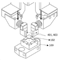
도 1을 참조하면, 픽 앤 플레이스 공정(1) 동안 전자 부품(102) 그룹을 이송하기 위한 예시적인 방법 흐름이 도시되어 있다. 상기 방법(1)은 (i) 복수의 픽업 헤드(101)를 갖는 픽업 및 플레이스 장치에 의해 상기 전자 부품(102) 그룹을 특정 위치에 배치하는 단계로서, 상기 특정 위치는 적어도 4 개의 네스트 벽(111)으로부터 각각 떨어지게 미리 결정된 XY 오프셋을 갖는 네스트(109)이고, 상기 미리 결정된 XY 오프셋은 상기 네스트 벽에 대해 200um 내지 300um의 범위에 있고(311); (ii) 상기 네스트 벽(111)에 대하여, 상기 그룹 내의 각 전자 부품(102)의 XY 위치를 결정하기 위해, 적어도 하나의 사전 정렬기 비전 검사 시스템에 의해 상기 전자 부품(102) 그룹의 적어도 하나의 이미지를 캡처하는 단계(103)로서, 상기 네스트 벽(111)은 0.1 mm 내지 1.0 mm 범위의 고정 두께를 갖고; (iii) 상기 네스트 벽(111)에 대하여 상기 그룹내의 모든 전자 부품(102)의 XY 위치가 미리 결정된 오프셋 값 내에 있으면, 적어도 하나의 정렬기 모듈(2)이 상기 그룹내의 각각의 전자 부품(102)을 서로에 대해 정렬시키는 단계(105)로서, 상기 전자 부품(102)의 크기 범위는 2x2mm와 7x7mm 사이이고; (iv) 상기 네스트 벽(111)에 대하여 상기 그룹내의 임의의 전자 부품(102)의 XY 위치가 미리 결정된 오프셋 값 내에 있지 않으면, 적어도 하나의 픽업 메커니즘이 전자 부품(102)의 상기 그룹을 픽업하여, 적어도 하나의 리젝트 빈으로 전달하거나, 또는 사용자가 상이한 미리 결정된 오프셋 값을 갖는 상기 그룹내의 영향 받은 전자 부품(102)을 재검사하는 단계(107)로 수행된다.Referring to FIG. 1 , an exemplary method flow for transferring a group of
상기 전자 부품(102)의 재검사 후에, 상기 네스트 벽(111)에 대한 상기 그룹내의 임의의 전자 부품(102)의 XY 위치가 여전히 미리 결정된 오프셋 값 내에 있지 않은 상황에서, 사용자는 미리 결정된 오프셋 값을 재확인하거나, 상기 전자 부품(102)의 정렬을 물리적으로 조정할 것이다. 일반적으로, 사용자는 다수의 재검사주기를 설정할 수 있다. 한계에 도달하면, 전자 부품(102)이 자동으로 리젝트된다.After re-inspection of the
도 2a 및 도 2b에 도시된 바와 같이, 상기 정렬기 모듈(2)은 양의 Y-축 방향을 따라 이동하는 적어도 하나의 제 1 및 제 2 Y-축 정렬기 아암(201, 203) 및 양의 X-축 방향을 따라 이동하는 적어도 하나의 제 1 및 제 2 X-축 정렬기 아암(205)을 포함한다. 상기 제 1 및 제 2 Y-축 정렬기 아암(201, 203)은 Y-축 액추에이터(209)에 작동되고 상기 제 1 및 제 2 X-축 정렬기 아암(205, 207)은 X-축 액추에이터(211)에 의해 작동되고, 그것들은 상기 제 1 Y-축 정렬기 아암(201)이 상기 제 2 Y-축 정렬기 아암(203)에 대향하며, 상기 제 1 X-축 정렬기 아암(205)이 상기 제 2 X-축 정렬기 아암(207)에 대향하는 구성으로 배열된다. 부가적으로, 상기 제 1 및 제 2 Y-축 정렬기 아암(201, 203), 및 상기 제 1 및 제 2 X-축 정렬기 아암(205, 207)은 상기 전자 부품(102)을 향하고 있다. 상기 정렬기 모듈(2)은 Z-축 방향을 따라 이동하도록 정렬기 모듈(2)을 작동시키는 Z-축 액추에이터(213)를 더 포함한다.2A and 2B , the
단계(iii)에 더하여, 네스트 벽(111)에 대하여 상기 그룹내의 모든 전자 부품(102)의 XY 위치가 미리 결정된 오프셋 값 내에 있으면, 적어도 하나의 정렬기 모듈(2)이 상기 그룹내의 각각의 전자 부품(102)을 서로에 대해 정렬시키고(105), 이는 다음의 하위 단계들: (a)상기 정렬기 모듈(2)이 Z-축 액추에이터(213)에 의해 작동되어, 제 1 Z-위치로부터 사전 설정된 제 2 Z-위치로 아래로 이동하는 단계로서, 상기 사전 설정된 제 2 Z-위치는 바람직하게는 상기 전자 부품(102)의 상단면보다 낮으며(301), 예를 들어 상기 제 1 및 제 2 Y-축 정렬기 아암 팁(401) 및 X-축 정렬기 아암 팁(403)의 바닥면은 도 4a 및 도 4b를 참조하여 상기 전자 부품(102) 그룹의 상단면보다 낮을 것이고; (b)상기 네스트(109)의 상단에 위치한 상기 제 1 Y-축 정렬기 아암(201)에 의해 상기 전자 부품(102)의 Y-축 오프셋 및 각도를 정렬하는 단계로서, 상기 제 1 Y-축 정렬기 아암(201)은 Y-축 액추에이터(209)에 의해 작동되고(303); (c)상기 네스트(109)의 좌측에 위치한 상기 제 1 X-축 정렬기 아암(205)에 의해 상기 전자 부품(102)의 X-축 오프셋 및 각도를 정렬하는 단계로서, 상기 제 1 X-축 정렬기 아암(205)은 X-축 액추에이터(211)에 의해 작동되고(305); (d)상기 네스트(109)의 바닥에 위치한 상기 제 2 Y-축 정렬기 아암(203)에 의해 상기 전자 부품(102)의 Y-축 오프셋 및 각도를 정렬하는 단계로서, 상기 제 2 Y-축 정렬기 아암(203)은 상기 Y-축 액추에이터(209)에 의해 작동되고(307); (e)상기 네스트(109)의 우측에 위치한 상기 제 2 X-축 정렬기 아암(207)에 의해 상기 전자 부품(102)의 X-축 오프셋 및 각도를 정렬하는 단계로서, 상기 제 2 X-축 정렬기 아암(207)은 상기 X-축 액추에이터(211)에 의해 작동되고(309); (f)상기 제 1 및 제 2 Y-축 정렬기 아암(201, 203), 및 상기 제 1 및 제 2 X-축 정렬기 아암(205, 207)은 다시 대기 위치로 이동하고(311); (g)상기 정렬기 모듈(2)은 상기 제 1 Z-위치로 다시 이동하고(313); 마지막으로 (h)상기 전자 부품(102)이 상기 전자 부품들(102)이 정렬 비전 검사를 통과하면, 상기 복수의 픽업 헤드들에 의해 일회성 동작으로 픽업되고 출력 캐리어 상에 플레이스될 것이며, 상기 복수의 픽업 헤드는 도 3a에 도시된 바와 같이 액추에이터(도시되지 않음)에 의해 작동된다(315).In addition to step (iii), if the XY positions of all
다른 구성에서, 도 3b를 참조하면, 상기 네스트(109)의 우측에 위치한 상기 제 2 X-축 정렬기 아암(207)에 의해 상기 전자 부품(102)의 X-축 오프셋 및 각도를 정렬하는 단계로서, 상기 제 2 X-축 정렬기 아암(207)이 상기 X-축 액추에이터(211)(309)에 의해 작동되는 상기 단계(e)는 상기 네스트(109)의 바닥에 위치한 상기 제 2 Y-축 정렬기 아암(203)에 의해 상기 전자 부품(102)의 Y-축 오프셋 및 각도를 정렬하는 단계로서, 상기 제 2 Y-축 정렬기 아암(203)은 상기 Y-축 액추에이터(209)에 의해 작동되는 단계(307)인 단계(d) 이전에, 그리고 상기 네스트(109)의 상단에 위치한 상기 제 1 Y-축 정렬기 아암(201)에 의해 상기 전자 부품(102)의 Y-축 오프셋 및 각도를 정렬하는 단계로서, 상기 제 1 Y-축 정렬기 아암(201)은 Y-축 액추에이터(209)에 의해 작동되는 단계(303)인 단계 (b) 이후에 수행될 수 있다. 한편, 상기 네스트(109)의 바닥에 위치한 상기 제 2 Y-축 정렬기 아암(203)에 의해 상기 전자 부품의 Y-축 오프셋 및 각도를 정렬하는 단계로서, 상기 제 2 Y-축 정렬기 아암(203)은 상기 Y-축 액추에이터(209)에 의해 작동되는 단계(307)인 단계 (d) 다음에, 상기 네스트(109)의 좌측에 위치한 상기 제 1 X-축 정렬기 아암(205)에 의해 상기 전자 부품(102)의 X-축 오프셋 및 각도를 정렬하는 단계로서, 상기 제 1 X-축 정렬기 아암(205)은 X-축 액추에이터(211)에 의해 작동되는 단계(305)인 단계(c)가 어어질 수 있고, 다음의 하위 단계들은 도 3a에 예시된 바와 같다. 상기 제 1 및 제 2 Y-축 정렬기 아암(201, 203), 및 상기 제 1 및 제 2 X-축 정렬기 아암(205, 207)은 스프링 작동식 정렬기 아암, 공기 작동식 정렬기 아암, 보이스 코일 액추에이터 등을 포함한다. 또한, 상기 방법은 단일 픽 액 플레이스 공정에서 다수의 크기 또는 다수의 유형의 전자 부품(102)을 제공하기 위하여, 상기 제 1 및 제 2 Y-축 정렬기 아암(201, 203), 및 상기 제 1 및 제 2 X-축 정렬기 아암(205, 207)의 길이 변환을 더 포함한다. In another configuration, referring to FIG. 3B , aligning the X-axis offset and angle of the
Claims (10)
(i) 복수의 픽업 헤드를 갖는 픽 앤 플레이스 장치에 의해 상기 전자 부품(102) 그룹을 특정 위치에 플레이스하는 단계(101)를 포함하는 방법으로서, 상기 특정 위치는 4 개의 네스트 벽(111)으로 이루어진 정사각형 형태이며, 4 개의 네스트 벽(111)으로부터 각각 떨어지도록 미리 결정된 XY 오프셋을 갖는 네스트이고;
상기 픽 앤 플레이스 공정(1) 동안 전자 부품(102) 그룹을 이송하는 방법은 상기 단계(i) 이후에, 다음의 단계들:
(ii) 상기 네스트 벽(111)에 대하여, 상기 전자 부품(102) 그룹 내의 각 전자 부품(102)의 XY 위치를 결정하기 위해, 적어도 하나의 사전 정렬기 비전 검사 시스템에 의해 상기 전자 부품(102) 그룹의 적어도 하나의 이미지를 캡처하는 단계(103);
(iii) 상기 네스트 벽(111)에 대하여, 상기 전자 부품(102) 그룹 내의 모든 전자 부품(102)의 XY 위치가 미리 결정된 오프셋 값 내에 있으면, 적어도 하나의 정렬기 모듈(2)이 상기 전자 부품(102) 그룹내의 각각의 전자 부품(102)을 서로에 대해 정렬시키는 단계(105);
(iv) 상기 네스트 벽(111)에 대하여, 상기 전자 부품(102) 그룹내의 적어도 하나의 전자 부품(102)의 XY 위치가 미리 결정된 오프셋 값 내에 있지 않으면, 적어도 하나의 픽업 메커니즘이 상기 전자 부품(102) 그룹을 픽업하여, 적어도 하나의 리젝트 빈으로 전달하거나, 또는 사용자는 상기 전자 부품(102) 그룹내의 영향 받은(affected) 전자 부품(102)을 상이한 미리 결정된 오프셋 값으로 재검사하는 단계(107);
를 추가로 포함하는, 픽 앤 플레이스 공정(1) 동안 전자 부품(102) 그룹을 이송하는 방법. A method for transferring a group of electronic components (102) during a pick and place process (1), comprising:
(i) placing (101) the group of electronic components (102) at a specific location by a pick-and-place device having a plurality of pick-up heads, wherein the specific location is defined by four nested walls (111) a nest with a predetermined XY offset so as to be separated from each of the four nest walls 111;
The method for transporting a group of electronic components 102 during the pick and place process (1) includes, after step (i), the following steps:
(ii) at least one pre-aligner vision inspection system to determine the XY position of each electronic component 102 within the group of electronic components 102 relative to the nest wall 111 . ) capturing (103) at least one image of the group;
(iii) with respect to the nest wall 111 , if the XY positions of all electronic components 102 within the group of electronic components 102 are within a predetermined offset value, then at least one aligner module 2 determines whether the electronic component (102) aligning (105) each electronic component (102) in the group relative to each other;
(iv) if the XY position of at least one electronic component 102 within the group of electronic components 102 with respect to the nest wall 111 is not within a predetermined offset value, at least one pickup mechanism 102) picking up a group and passing it to at least one reject bin, or a user retesting (107) the affected electronic components (102) in the group of electronic components (102) with different predetermined offset values; );
A method for transferring a group of electronic components (102) during a pick and place process (1), further comprising a.
(a) 상기 정렬기 모듈(2)이 Z-축 액추에이터(213)에 의해 작동되어, 제 1 Z-위치로부터 사전 설정된 제 2 Z-위치로 아래로 이동하는 단계로서, 이에 의해 상기 사전 설정된 제 2 Z-위치가 상기 전자 부품(102) 그룹의 상단면보다 낮아지게 하는 단계(301);
(b) 상기 네스트(109)의 측부에서 바라 볼 때, 상기 네스트(109)의 상단에 위치한 상기 제 1 Y-축 정렬기 아암(201)에 의해 상기 전자 부품(102) 그룹의 Y-축 오프셋 및 각도를 정렬하는 단계로서, 상기 제 1 Y-축 정렬기 아암(201)은 Y-축 액추에이터(209)에 의해 작동되는 단계(303);
(c) 상기 네스트(109)의 측부에서 바라 볼 때, 상기 네스트(109)의 좌측에 위치한 상기 제 1 X-축 정렬기 아암(205)에 의해 상기 전자 부품(102) 그룹의 X-축 오프셋 및 각도를 정렬하는 단계로서, 상기 제 1 X-축 정렬기 아암(205)은 X-축 액추에이터(211)에 의해 작동되는 단계(305);
(d) 상기 네스트(109)의 측부에서 바라 볼 때, 상기 네스트(109)의 바닥에 위치한 상기 제 2 Y-축 정렬기 아암(203)에 의해 상기 전자 부품(102) 그룹의 Y-축 오프셋 및 각도를 정렬하는 단계로서, 상기 제 2 Y-축 정렬기 아암(203)은 상기 Y-축 액추에이터(209)에 의해 작동되는 단계(307);
(e) 상기 네스트(109)의 측부에서 바라 볼 때, 상기 네스트(109)의 우측에 위치한 상기 제 2 X-축 정렬기 아암(207)에 의해 상기 전자 부품(102) 그룹의 X-축 오프셋 및 각도를 정렬하는 단계로서, 상기 제 2 X-축 정렬기 아암(207)은 상기 X-축 액추에이터(211)에 의해 작동되는 단계(309);
(f) 상기 제 1 및 제 2 Y-축 정렬기 아암(201, 203), 및 상기 제 1 및 제 2 X-축 정렬기 아암(205, 207)은 다시 대기 위치로 이동하는 단계(311);
(g) 상기 정렬기 모듈(2)은 상기 제 1 Z-위치로 다시 이동하는 단계(313);
(h) 상기 전자 부품(102) 그룹은 상기 전자 부품(102) 그룹이 상기 적어도 하나의 사전 정렬기 비전 검사 시스템에 의한 정렬 비전 검사를 통과한 경우, 일회성 동작으로 상기 복수의 픽업 헤드에 의해 픽업되고 캐리어 상에 플레이스되는 단계로서, 상기 복수의 픽업 헤드는 액추에이터에 의해 작동되는 단계(315);
를 포함하는, 픽 앤 플레이스 공정(1) 동안 전자 부품(102) 그룹을 이송하는 방법.3. The method according to claim 2, wherein step (iii) comprises the following sub-steps (3A):
(a) the aligner module (2) is actuated by a Z-axis actuator (213) to move down from a first Z-position to a second preset Z-position, whereby the preset second 2 making the Z-position lower than the top surface of the group of electronic components (102) (301);
(b) the Y-axis offset of the group of electronic components 102 by the first Y-axis aligner arm 201 located on top of the nest 109 when viewed from the side of the nest 109 . and aligning the angle, wherein the first Y-axis aligner arm (201) is actuated (303) by a Y-axis actuator (209);
(c) the X-axis offset of the group of electronic components 102 by the first X-axis aligner arm 205 located to the left of the nest 109, when viewed from the side of the nest 109 and aligning the angle, wherein the first X-axis aligner arm (205) is actuated (305) by an X-axis actuator (211);
(d) the Y-axis offset of the group of electronic components 102 by the second Y-axis aligner arm 203 located at the bottom of the nest 109 when viewed from the side of the nest 109 . and aligning the angle, wherein the second Y-axis aligner arm (203) is actuated (307) by the Y-axis actuator (209);
(e) the X-axis offset of the group of electronic components 102 by the second X-axis aligner arm 207 located to the right of the nest 109 when viewed from the side of the nest 109 . and aligning the angle, wherein the second X-axis aligner arm (207) is actuated (309) by the X-axis actuator (211);
(f) the first and second Y-axis aligner arms 201, 203, and the first and second X-axis aligner arms 205 and 207, moving back to the standby position (311);
(g) moving (313) the aligner module (2) back to the first Z-position;
(h) the group of electronic components 102 is picked up by the plurality of pickup heads in a one-time operation when the group of electronic components 102 has passed alignment vision inspection by the at least one pre-aligner vision inspection system and placed on a carrier, wherein the plurality of pickup heads are actuated by an actuator (315);
A method for transferring a group of electronic components (102) during a pick and place process (1) comprising:
(a) 상기 정렬기 모듈(2)이 Z-축 액추에이터(213)에 의해 작동되어, 제 1 Z-위치로부터 사전 설정된 제 2 Z-위치로 아래로 이동하는 단계로서, 이에 의해 상기 사전 설정된 제 2 Z-위치가 상기 전자 부품(102) 그룹의 상단면보다 낮아지게 되는 단계(301);
(b) 상기 네스트(109)의 측부에서 바라 볼 때, 상기 네스트(109)의 상단에 위치한 상기 제 1 Y-축 정렬기 아암(201)에 의해 상기 전자 부품(102) 그룹의 Y-축 오프셋 및 각도를 정렬하는 단계로서, 상기 제 1 Y-축 정렬기 아암(201)은 Y-축 액추에이터(209)에 의해 작동되는 단계(303);
(e) 상기 네스트(109)의 측부에서 바라 볼 때, 상기 네스트(109)의 우측에 위치한 상기 제 2 X-축 정렬기 아암(207)에 의해 상기 전자 부품(102) 그룹의 X-축 오프셋 및 각도를 정렬하는 단계로서, 상기 제 2 X-축 정렬기 아암(207)은 X-축 액추에이터(211)에 의해 작동되는 단계(309);
(d) 상기 네스트(109)의 측부에서 바라 볼 때, 상기 네스트(109)의 바닥에 위치한 상기 제 2 Y-축 정렬기 아암(203)에 의해 상기 전자 부품(102) 그룹의 Y-축 오프셋 및 각도를 정렬하는 단계로서, 상기 제 2 Y-축 정렬기 아암(203)은 상기 Y-축 액추에이터(209)에 의해 작동되는 단계(307);
(c) 상기 네스트(109)의 측부에서 바라 볼 때, 상기 네스트(109)의 좌측에 위치한 상기 제 1 X-축 정렬기 아암(205)에 의해 상기 전자 부품(102) 그룹의 X-축 오프셋 및 각도를 정렬하는 단계로서, 상기 제 1 X-축 정렬기 아암(205)은 상기 X-축 액추에이터(211)에 의해 작동되는 단계(305);
(f) 상기 제 1 및 제 2 Y-축 정렬기 아암(201, 203), 및 상기 제 1 및 제 2 X-축 정렬기 아암(205, 207)이 다시 대기 위치로 이동하는 단계(311);
(g) 상기 정렬기 모듈(2)이 상기 제 1 Z-위치로 다시 이동하는 단계(313);
(h) 상기 전자 부품(102) 그룹은 상기 전자 부품(102)이 상기 적어도 하나의 사전 정렬기 비전 검사 시스템에 의한 정렬 비전 검사를 통과한 경우, 일회성 동작으로 상기 복수의 픽업 헤드에 의해 픽업되고 캐리어 상에 플레이스되는 단계로서, 상기 복수의 픽업 헤드는 액추에이터에 의해 작동되는 단계(315);
를 더 포함하는, 픽 앤 플레이스 공정(1) 동안 전자 부품(102) 그룹을 이송하는 방법.3. The method according to claim 2, wherein the method for transferring a group of electronic components (102) during the pick and place process (1) comprises the following steps (3B):
(a) the aligner module (2) is actuated by a Z-axis actuator (213) to move down from a first Z-position to a second preset Z-position, whereby the preset second 2 Z-position being lower than the top surface of the group of electronic components (102) (301);
(b) the Y-axis offset of the group of electronic components 102 by the first Y-axis aligner arm 201 located on top of the nest 109 when viewed from the side of the nest 109 . and aligning the angle, wherein the first Y-axis aligner arm (201) is actuated (303) by a Y-axis actuator (209);
(e) the X-axis offset of the group of electronic components 102 by the second X-axis aligner arm 207 located to the right of the nest 109 when viewed from the side of the nest 109 . and aligning the angle, wherein the second X-axis aligner arm (207) is actuated (309) by an X-axis actuator (211);
(d) the Y-axis offset of the group of electronic components 102 by the second Y-axis aligner arm 203 located at the bottom of the nest 109 when viewed from the side of the nest 109 . and aligning the angle, wherein the second Y-axis aligner arm (203) is actuated (307) by the Y-axis actuator (209);
(c) the X-axis offset of the group of electronic components 102 by the first X-axis aligner arm 205 located to the left of the nest 109, when viewed from the side of the nest 109 and aligning the angle, wherein the first X-axis aligner arm (205) is actuated (305) by the X-axis actuator (211);
(f) the first and second Y-axis aligner arms (201, 203), and the first and second X-axis aligner arms (205, 207) moving back to the standby position (311);
(g) moving (313) the aligner module (2) back to the first Z-position;
(h) the group of electronic components 102 is picked up by the plurality of pickup heads in a one-time operation when the electronic components 102 have passed alignment vision inspection by the at least one pre-aligner vision inspection system; placing on a carrier, wherein the plurality of pickup heads are actuated by an actuator (315);
A method for transferring a group of electronic components (102) during a pick and place process (1), further comprising:
3. The method according to claim 2, wherein the method for transferring a group of electronic components (102) during the pick and place process (1) comprises: to provide multiple sizes or multiple types of electronic components (102) in a single pick and place process; a pick and place process (1) further comprising length transformation of the first and second Y-axis aligner arms (201, 203), and the first and second X-axis aligner arms (205, 207) ) while transporting a group of electronic components 102 .
Applications Claiming Priority (2)
| Application Number | Priority Date | Filing Date | Title |
|---|---|---|---|
| MYPI2019006868 | 2019-11-22 | ||
| MYPI2019006868 | 2019-11-22 |
Publications (2)
| Publication Number | Publication Date |
|---|---|
| KR20210064023A KR20210064023A (en) | 2021-06-02 |
| KR102434661B1 true KR102434661B1 (en) | 2022-08-19 |
Family
ID=75745582
Family Applications (1)
| Application Number | Title | Priority Date | Filing Date |
|---|---|---|---|
| KR1020200063372A KR102434661B1 (en) | 2019-11-22 | 2020-05-27 | A method for conveying a group of electronic components during pick and place process |
Country Status (3)
| Country | Link |
|---|---|
| KR (1) | KR102434661B1 (en) |
| PH (1) | PH12020050193A1 (en) |
| TW (1) | TWI718064B (en) |
Citations (1)
| Publication number | Priority date | Publication date | Assignee | Title |
|---|---|---|---|---|
| KR101697119B1 (en) | 2016-07-07 | 2017-01-18 | 에스에스오트론 주식회사 | apparatus for vision inspection of semiconductor |
Family Cites Families (7)
| Publication number | Priority date | Publication date | Assignee | Title |
|---|---|---|---|---|
| US8770909B2 (en) * | 2007-01-31 | 2014-07-08 | Kaufmann Engineered Group | Layer formation table and process |
| KR20100034615A (en) * | 2008-09-24 | 2010-04-01 | 주식회사 하이닉스반도체 | Method for exposuring of photomask |
| KR100979721B1 (en) * | 2008-12-04 | 2010-09-03 | (주)에이피텍 | Combined apparatus of vision inspection and sorting for semiconductor die |
| JP5472214B2 (en) * | 2011-06-20 | 2014-04-16 | 株式会社安川電機 | Picking system |
| CN107134422A (en) * | 2016-02-29 | 2017-09-05 | 上海微电子装备(集团)股份有限公司 | Chip bonding device and method |
| JP7047249B2 (en) * | 2017-01-10 | 2022-04-05 | オムロン株式会社 | Image processing system, image processing device, work pickup method, and work pickup program |
| CN109516203B (en) * | 2018-12-10 | 2020-07-21 | 温州大学瓯江学院 | Adsorption type station transposition device based on rotating structure |
-
2020
- 2020-05-26 TW TW109117432A patent/TWI718064B/en active
- 2020-05-27 KR KR1020200063372A patent/KR102434661B1/en active IP Right Grant
- 2020-06-29 PH PH12020050193A patent/PH12020050193A1/en unknown
Patent Citations (1)
| Publication number | Priority date | Publication date | Assignee | Title |
|---|---|---|---|---|
| KR101697119B1 (en) | 2016-07-07 | 2017-01-18 | 에스에스오트론 주식회사 | apparatus for vision inspection of semiconductor |
Also Published As
| Publication number | Publication date |
|---|---|
| KR20210064023A (en) | 2021-06-02 |
| TWI718064B (en) | 2021-02-01 |
| TW202120279A (en) | 2021-06-01 |
| PH12020050193A1 (en) | 2021-05-31 |
Similar Documents
| Publication | Publication Date | Title |
|---|---|---|
| KR101378326B1 (en) | Transfer apparatus for handling electronic components | |
| KR100722185B1 (en) | System for processing electronic devices | |
| US20060056955A1 (en) | Sawing and sorting system | |
| KR100979721B1 (en) | Combined apparatus of vision inspection and sorting for semiconductor die | |
| KR20070011472A (en) | Chip component carrying method and system, and visual inspection method and system | |
| KR101120938B1 (en) | Handling system for inspecting and sorting electronic components | |
| KR20080074530A (en) | Sawing and handling apparatus for semiconductor package | |
| KR101831256B1 (en) | Semiconductor Strip Align Apparatus And Semiconductor Strip Align Method Using The Same | |
| KR102159183B1 (en) | Device handler and method for handling device | |
| KR101812677B1 (en) | System and method for flexible high speed transfer of semiconductor components | |
| JP2000205848A (en) | Visual inspection facility for module | |
| JP2995435B2 (en) | Automatic chip sorting and conveying device | |
| KR102434661B1 (en) | A method for conveying a group of electronic components during pick and place process | |
| TW202320202A (en) | System and process for sorting die from wafer using angled wafer table and angled turret | |
| JP2004121990A (en) | Work conveyance and storage device and method | |
| KR101790546B1 (en) | Pick and place system for wafer ring frame type | |
| KR101454320B1 (en) | Strip loading Apparatus for Semiconductor Package Manufacturing Equipment | |
| KR20150005269A (en) | Cutting and Loading Apparatus of Semiconductor Materials | |
| KR100639400B1 (en) | Lid pick and place equipment | |
| KR102642099B1 (en) | Package cutting and sorting system with air dryer | |
| KR102641625B1 (en) | Package cutting and sorting system with reject bin | |
| TWI836715B (en) | Semiconductor component pickup device and operation control method thereof | |
| JP7328848B2 (en) | Die bonding apparatus and semiconductor device manufacturing method | |
| KR102124318B1 (en) | LED module sorting system | |
| JP5604355B2 (en) | Semiconductor chip inspection and sorting apparatus and inspection and sorting method |
Legal Events
| Date | Code | Title | Description |
|---|---|---|---|
| E902 | Notification of reason for refusal | ||
| AMND | Amendment | ||
| E601 | Decision to refuse application | ||
| AMND | Amendment | ||
| X701 | Decision to grant (after re-examination) | ||
| GRNT | Written decision to grant |