KR102396074B1 - Light-emitting device - Google Patents
Light-emitting device Download PDFInfo
- Publication number
- KR102396074B1 KR102396074B1 KR1020160184194A KR20160184194A KR102396074B1 KR 102396074 B1 KR102396074 B1 KR 102396074B1 KR 1020160184194 A KR1020160184194 A KR 1020160184194A KR 20160184194 A KR20160184194 A KR 20160184194A KR 102396074 B1 KR102396074 B1 KR 102396074B1
- Authority
- KR
- South Korea
- Prior art keywords
- light emitting
- light
- reflective layer
- emitting device
- layer
- Prior art date
Links
- 238000000034 method Methods 0.000 claims description 17
- 239000010410 layer Substances 0.000 description 265
- 239000000853 adhesive Substances 0.000 description 62
- 230000001070 adhesive effect Effects 0.000 description 62
- 238000005520 cutting process Methods 0.000 description 61
- 239000002245 particle Substances 0.000 description 49
- 239000000463 material Substances 0.000 description 47
- 239000012790 adhesive layer Substances 0.000 description 40
- 238000006243 chemical reaction Methods 0.000 description 39
- 238000004519 manufacturing process Methods 0.000 description 31
- 239000004065 semiconductor Substances 0.000 description 25
- 239000000758 substrate Substances 0.000 description 22
- 239000000843 powder Substances 0.000 description 15
- 238000009792 diffusion process Methods 0.000 description 11
- 230000004907 flux Effects 0.000 description 11
- 239000004973 liquid crystal related substance Substances 0.000 description 11
- 230000000875 corresponding effect Effects 0.000 description 10
- 239000011159 matrix material Substances 0.000 description 9
- 230000008569 process Effects 0.000 description 9
- VYPSYNLAJGMNEJ-UHFFFAOYSA-N Silicium dioxide Chemical compound O=[Si]=O VYPSYNLAJGMNEJ-UHFFFAOYSA-N 0.000 description 8
- -1 for example Substances 0.000 description 8
- TWNQGVIAIRXVLR-UHFFFAOYSA-N oxo(oxoalumanyloxy)alumane Chemical compound O=[Al]O[Al]=O TWNQGVIAIRXVLR-UHFFFAOYSA-N 0.000 description 7
- 238000005507 spraying Methods 0.000 description 7
- PXHVJJICTQNCMI-UHFFFAOYSA-N Nickel Chemical compound [Ni] PXHVJJICTQNCMI-UHFFFAOYSA-N 0.000 description 6
- GWEVSGVZZGPLCZ-UHFFFAOYSA-N Titan oxide Chemical compound O=[Ti]=O GWEVSGVZZGPLCZ-UHFFFAOYSA-N 0.000 description 6
- UMIVXZPTRXBADB-UHFFFAOYSA-N benzocyclobutene Chemical compound C1=CC=C2CCC2=C1 UMIVXZPTRXBADB-UHFFFAOYSA-N 0.000 description 6
- 239000011248 coating agent Substances 0.000 description 6
- 238000000576 coating method Methods 0.000 description 6
- 238000010438 heat treatment Methods 0.000 description 6
- BASFCYQUMIYNBI-UHFFFAOYSA-N platinum Chemical compound [Pt] BASFCYQUMIYNBI-UHFFFAOYSA-N 0.000 description 6
- 229920000139 polyethylene terephthalate Polymers 0.000 description 6
- 239000005020 polyethylene terephthalate Substances 0.000 description 6
- 239000004642 Polyimide Substances 0.000 description 5
- 238000005259 measurement Methods 0.000 description 5
- 229920001721 polyimide Polymers 0.000 description 5
- 229920001296 polysiloxane Polymers 0.000 description 5
- 238000007650 screen-printing Methods 0.000 description 5
- 239000004925 Acrylic resin Substances 0.000 description 4
- 229920000178 Acrylic resin Polymers 0.000 description 4
- 239000011651 chromium Substances 0.000 description 4
- 239000010949 copper Substances 0.000 description 4
- 238000013461 design Methods 0.000 description 4
- 238000009826 distribution Methods 0.000 description 4
- 239000010931 gold Substances 0.000 description 4
- BCCOBQSFUDVTJQ-UHFFFAOYSA-N octafluorocyclobutane Chemical compound FC1(F)C(F)(F)C(F)(F)C1(F)F BCCOBQSFUDVTJQ-UHFFFAOYSA-N 0.000 description 4
- 235000019407 octafluorocyclobutane Nutrition 0.000 description 4
- 230000003287 optical effect Effects 0.000 description 4
- 239000011241 protective layer Substances 0.000 description 4
- 238000004088 simulation Methods 0.000 description 4
- 239000004593 Epoxy Substances 0.000 description 3
- OAICVXFJPJFONN-UHFFFAOYSA-N Phosphorus Chemical compound [P] OAICVXFJPJFONN-UHFFFAOYSA-N 0.000 description 3
- XLOMVQKBTHCTTD-UHFFFAOYSA-N Zinc monoxide Chemical compound [Zn]=O XLOMVQKBTHCTTD-UHFFFAOYSA-N 0.000 description 3
- 229910052782 aluminium Inorganic materials 0.000 description 3
- 230000008859 change Effects 0.000 description 3
- 230000001678 irradiating effect Effects 0.000 description 3
- 229910052751 metal Inorganic materials 0.000 description 3
- 239000002184 metal Substances 0.000 description 3
- 150000004767 nitrides Chemical class 0.000 description 3
- 238000001556 precipitation Methods 0.000 description 3
- 239000002096 quantum dot Substances 0.000 description 3
- 235000012239 silicon dioxide Nutrition 0.000 description 3
- 239000000377 silicon dioxide Substances 0.000 description 3
- 239000012780 transparent material Substances 0.000 description 3
- SKJCKYVIQGBWTN-UHFFFAOYSA-N (4-hydroxyphenyl) methanesulfonate Chemical compound CS(=O)(=O)OC1=CC=C(O)C=C1 SKJCKYVIQGBWTN-UHFFFAOYSA-N 0.000 description 2
- PFNQVRZLDWYSCW-UHFFFAOYSA-N (fluoren-9-ylideneamino) n-naphthalen-1-ylcarbamate Chemical compound C12=CC=CC=C2C2=CC=CC=C2C1=NOC(=O)NC1=CC=CC2=CC=CC=C12 PFNQVRZLDWYSCW-UHFFFAOYSA-N 0.000 description 2
- IHGSAQHSAGRWNI-UHFFFAOYSA-N 1-(4-bromophenyl)-2,2,2-trifluoroethanone Chemical compound FC(F)(F)C(=O)C1=CC=C(Br)C=C1 IHGSAQHSAGRWNI-UHFFFAOYSA-N 0.000 description 2
- WUPHOULIZUERAE-UHFFFAOYSA-N 3-(oxolan-2-yl)propanoic acid Chemical compound OC(=O)CCC1CCCO1 WUPHOULIZUERAE-UHFFFAOYSA-N 0.000 description 2
- MARUHZGHZWCEQU-UHFFFAOYSA-N 5-phenyl-2h-tetrazole Chemical compound C1=CC=CC=C1C1=NNN=N1 MARUHZGHZWCEQU-UHFFFAOYSA-N 0.000 description 2
- 229910018072 Al 2 O 3 Inorganic materials 0.000 description 2
- PIGFYZPCRLYGLF-UHFFFAOYSA-N Aluminum nitride Chemical compound [Al]#N PIGFYZPCRLYGLF-UHFFFAOYSA-N 0.000 description 2
- VYZAMTAEIAYCRO-UHFFFAOYSA-N Chromium Chemical compound [Cr] VYZAMTAEIAYCRO-UHFFFAOYSA-N 0.000 description 2
- RYGMFSIKBFXOCR-UHFFFAOYSA-N Copper Chemical compound [Cu] RYGMFSIKBFXOCR-UHFFFAOYSA-N 0.000 description 2
- BPQQTUXANYXVAA-UHFFFAOYSA-N Orthosilicate Chemical compound [O-][Si]([O-])([O-])[O-] BPQQTUXANYXVAA-UHFFFAOYSA-N 0.000 description 2
- 239000004697 Polyetherimide Substances 0.000 description 2
- 229910052581 Si3N4 Inorganic materials 0.000 description 2
- 229910004205 SiNX Inorganic materials 0.000 description 2
- 229910004298 SiO 2 Inorganic materials 0.000 description 2
- BQCADISMDOOEFD-UHFFFAOYSA-N Silver Chemical compound [Ag] BQCADISMDOOEFD-UHFFFAOYSA-N 0.000 description 2
- 239000005083 Zinc sulfide Substances 0.000 description 2
- 229910052784 alkaline earth metal Inorganic materials 0.000 description 2
- XAGFODPZIPBFFR-UHFFFAOYSA-N aluminium Chemical compound [Al] XAGFODPZIPBFFR-UHFFFAOYSA-N 0.000 description 2
- TZCXTZWJZNENPQ-UHFFFAOYSA-L barium sulfate Chemical compound [Ba+2].[O-]S([O-])(=O)=O TZCXTZWJZNENPQ-UHFFFAOYSA-L 0.000 description 2
- 229910052980 cadmium sulfide Inorganic materials 0.000 description 2
- 229910052804 chromium Inorganic materials 0.000 description 2
- 238000000748 compression moulding Methods 0.000 description 2
- 230000001276 controlling effect Effects 0.000 description 2
- 229910052802 copper Inorganic materials 0.000 description 2
- 238000010586 diagram Methods 0.000 description 2
- ZZEMEJKDTZOXOI-UHFFFAOYSA-N digallium;selenium(2-) Chemical compound [Ga+3].[Ga+3].[Se-2].[Se-2].[Se-2] ZZEMEJKDTZOXOI-UHFFFAOYSA-N 0.000 description 2
- 239000003822 epoxy resin Substances 0.000 description 2
- PCHJSUWPFVWCPO-UHFFFAOYSA-N gold Chemical compound [Au] PCHJSUWPFVWCPO-UHFFFAOYSA-N 0.000 description 2
- 229910052737 gold Inorganic materials 0.000 description 2
- 230000005484 gravity Effects 0.000 description 2
- 239000003112 inhibitor Substances 0.000 description 2
- 238000000691 measurement method Methods 0.000 description 2
- 239000000203 mixture Substances 0.000 description 2
- 238000012986 modification Methods 0.000 description 2
- 230000004048 modification Effects 0.000 description 2
- 238000000465 moulding Methods 0.000 description 2
- 229910052759 nickel Inorganic materials 0.000 description 2
- 229910052697 platinum Inorganic materials 0.000 description 2
- 239000004417 polycarbonate Substances 0.000 description 2
- 229920000515 polycarbonate Polymers 0.000 description 2
- 229920000647 polyepoxide Polymers 0.000 description 2
- 229920001601 polyetherimide Polymers 0.000 description 2
- 229920000642 polymer Polymers 0.000 description 2
- 239000010948 rhodium Substances 0.000 description 2
- 229910052710 silicon Inorganic materials 0.000 description 2
- 239000010703 silicon Substances 0.000 description 2
- HQVNEWCFYHHQES-UHFFFAOYSA-N silicon nitride Chemical compound N12[Si]34N5[Si]62N3[Si]51N64 HQVNEWCFYHHQES-UHFFFAOYSA-N 0.000 description 2
- 229910052814 silicon oxide Inorganic materials 0.000 description 2
- 229910052709 silver Inorganic materials 0.000 description 2
- 239000004332 silver Substances 0.000 description 2
- 239000002356 single layer Substances 0.000 description 2
- 239000000126 substance Substances 0.000 description 2
- OCGWQDWYSQAFTO-UHFFFAOYSA-N tellanylidenelead Chemical compound [Pb]=[Te] OCGWQDWYSQAFTO-UHFFFAOYSA-N 0.000 description 2
- 239000010936 titanium Substances 0.000 description 2
- 239000004408 titanium dioxide Substances 0.000 description 2
- LSGOVYNHVSXFFJ-UHFFFAOYSA-N vanadate(3-) Chemical compound [O-][V]([O-])([O-])=O LSGOVYNHVSXFFJ-UHFFFAOYSA-N 0.000 description 2
- 229910052984 zinc sulfide Inorganic materials 0.000 description 2
- NIXOWILDQLNWCW-UHFFFAOYSA-M Acrylate Chemical compound [O-]C(=O)C=C NIXOWILDQLNWCW-UHFFFAOYSA-M 0.000 description 1
- JBRZTFJDHDCESZ-UHFFFAOYSA-N AsGa Chemical compound [As]#[Ga] JBRZTFJDHDCESZ-UHFFFAOYSA-N 0.000 description 1
- IJGRMHOSHXDMSA-UHFFFAOYSA-N Atomic nitrogen Chemical compound N#N IJGRMHOSHXDMSA-UHFFFAOYSA-N 0.000 description 1
- MYMOFIZGZYHOMD-UHFFFAOYSA-N Dioxygen Chemical compound O=O MYMOFIZGZYHOMD-UHFFFAOYSA-N 0.000 description 1
- 240000001973 Ficus microcarpa Species 0.000 description 1
- KRHYYFGTRYWZRS-UHFFFAOYSA-M Fluoride anion Chemical compound [F-] KRHYYFGTRYWZRS-UHFFFAOYSA-M 0.000 description 1
- 229910005542 GaSb Inorganic materials 0.000 description 1
- JMASRVWKEDWRBT-UHFFFAOYSA-N Gallium nitride Chemical compound [Ga]#N JMASRVWKEDWRBT-UHFFFAOYSA-N 0.000 description 1
- 229910000677 High-carbon steel Inorganic materials 0.000 description 1
- GPXJNWSHGFTCBW-UHFFFAOYSA-N Indium phosphide Chemical compound [In]#P GPXJNWSHGFTCBW-UHFFFAOYSA-N 0.000 description 1
- 229910002665 PbTe Inorganic materials 0.000 description 1
- NPAQUWKUZAIRJE-UHFFFAOYSA-N S=[Se].[Zn].[Cd] Chemical compound S=[Se].[Zn].[Cd] NPAQUWKUZAIRJE-UHFFFAOYSA-N 0.000 description 1
- ATJFFYVFTNAWJD-UHFFFAOYSA-N Tin Chemical compound [Sn] ATJFFYVFTNAWJD-UHFFFAOYSA-N 0.000 description 1
- RTAQQCXQSZGOHL-UHFFFAOYSA-N Titanium Chemical compound [Ti] RTAQQCXQSZGOHL-UHFFFAOYSA-N 0.000 description 1
- 229910045601 alloy Inorganic materials 0.000 description 1
- 239000000956 alloy Substances 0.000 description 1
- MDPILPRLPQYEEN-UHFFFAOYSA-N aluminium arsenide Chemical compound [As]#[Al] MDPILPRLPQYEEN-UHFFFAOYSA-N 0.000 description 1
- MRPWWVMHWSDJEH-UHFFFAOYSA-N antimony telluride Chemical compound [SbH3+3].[SbH3+3].[TeH2-2].[TeH2-2].[TeH2-2] MRPWWVMHWSDJEH-UHFFFAOYSA-N 0.000 description 1
- 238000013459 approach Methods 0.000 description 1
- 229910052810 boron oxide Inorganic materials 0.000 description 1
- AQCDIIAORKRFCD-UHFFFAOYSA-N cadmium selenide Chemical compound [Cd]=[Se] AQCDIIAORKRFCD-UHFFFAOYSA-N 0.000 description 1
- LYQFWZFBNBDLEO-UHFFFAOYSA-M caesium bromide Chemical compound [Br-].[Cs+] LYQFWZFBNBDLEO-UHFFFAOYSA-M 0.000 description 1
- AIYUHDOJVYHVIT-UHFFFAOYSA-M caesium chloride Chemical compound [Cl-].[Cs+] AIYUHDOJVYHVIT-UHFFFAOYSA-M 0.000 description 1
- XQPRBTXUXXVTKB-UHFFFAOYSA-M caesium iodide Chemical compound [I-].[Cs+] XQPRBTXUXXVTKB-UHFFFAOYSA-M 0.000 description 1
- 239000000919 ceramic Substances 0.000 description 1
- 238000005253 cladding Methods 0.000 description 1
- LCUOIYYHNRBAFS-UHFFFAOYSA-N copper;sulfanylideneindium Chemical compound [Cu].[In]=S LCUOIYYHNRBAFS-UHFFFAOYSA-N 0.000 description 1
- 230000002596 correlated effect Effects 0.000 description 1
- 239000013078 crystal Substances 0.000 description 1
- 230000007423 decrease Effects 0.000 description 1
- JKWMSGQKBLHBQQ-UHFFFAOYSA-N diboron trioxide Chemical compound O=BOB=O JKWMSGQKBLHBQQ-UHFFFAOYSA-N 0.000 description 1
- 229910001873 dinitrogen Inorganic materials 0.000 description 1
- 229910001882 dioxygen Inorganic materials 0.000 description 1
- 230000000694 effects Effects 0.000 description 1
- 238000009713 electroplating Methods 0.000 description 1
- 238000005265 energy consumption Methods 0.000 description 1
- VTGARNNDLOTBET-UHFFFAOYSA-N gallium antimonide Chemical compound [Sb]#[Ga] VTGARNNDLOTBET-UHFFFAOYSA-N 0.000 description 1
- HZXMRANICFIONG-UHFFFAOYSA-N gallium phosphide Chemical compound [Ga]#P HZXMRANICFIONG-UHFFFAOYSA-N 0.000 description 1
- 239000007789 gas Substances 0.000 description 1
- 239000011521 glass Substances 0.000 description 1
- 239000010438 granite Substances 0.000 description 1
- 230000017525 heat dissipation Effects 0.000 description 1
- 239000001307 helium Substances 0.000 description 1
- 229910052734 helium Inorganic materials 0.000 description 1
- SWQJXJOGLNCZEY-UHFFFAOYSA-N helium atom Chemical compound [He] SWQJXJOGLNCZEY-UHFFFAOYSA-N 0.000 description 1
- WPYVAWXEWQSOGY-UHFFFAOYSA-N indium antimonide Chemical compound [Sb]#[In] WPYVAWXEWQSOGY-UHFFFAOYSA-N 0.000 description 1
- RPQDHPTXJYYUPQ-UHFFFAOYSA-N indium arsenide Chemical compound [In]#[As] RPQDHPTXJYYUPQ-UHFFFAOYSA-N 0.000 description 1
- 239000011810 insulating material Substances 0.000 description 1
- 238000003475 lamination Methods 0.000 description 1
- XCAUINMIESBTBL-UHFFFAOYSA-N lead(ii) sulfide Chemical compound [Pb]=S XCAUINMIESBTBL-UHFFFAOYSA-N 0.000 description 1
- 229910001960 metal nitrate Inorganic materials 0.000 description 1
- 239000002105 nanoparticle Substances 0.000 description 1
- 229910052757 nitrogen Inorganic materials 0.000 description 1
- BPUBBGLMJRNUCC-UHFFFAOYSA-N oxygen(2-);tantalum(5+) Chemical compound [O-2].[O-2].[O-2].[O-2].[O-2].[Ta+5].[Ta+5] BPUBBGLMJRNUCC-UHFFFAOYSA-N 0.000 description 1
- RVTZCBVAJQQJTK-UHFFFAOYSA-N oxygen(2-);zirconium(4+) Chemical compound [O-2].[O-2].[Zr+4] RVTZCBVAJQQJTK-UHFFFAOYSA-N 0.000 description 1
- 229920002120 photoresistant polymer Polymers 0.000 description 1
- 238000009832 plasma treatment Methods 0.000 description 1
- 238000007747 plating Methods 0.000 description 1
- 238000005498 polishing Methods 0.000 description 1
- 229920003229 poly(methyl methacrylate) Polymers 0.000 description 1
- 239000004926 polymethyl methacrylate Substances 0.000 description 1
- 230000001376 precipitating effect Effects 0.000 description 1
- 238000003825 pressing Methods 0.000 description 1
- 238000002310 reflectometry Methods 0.000 description 1
- 238000009877 rendering Methods 0.000 description 1
- 230000004044 response Effects 0.000 description 1
- 229910052703 rhodium Inorganic materials 0.000 description 1
- MHOVAHRLVXNVSD-UHFFFAOYSA-N rhodium atom Chemical compound [Rh] MHOVAHRLVXNVSD-UHFFFAOYSA-N 0.000 description 1
- 229910052594 sapphire Inorganic materials 0.000 description 1
- 239000010980 sapphire Substances 0.000 description 1
- GGYFMLJDMAMTAB-UHFFFAOYSA-N selanylidenelead Chemical compound [Pb]=[Se] GGYFMLJDMAMTAB-UHFFFAOYSA-N 0.000 description 1
- 229910000679 solder Inorganic materials 0.000 description 1
- 239000002904 solvent Substances 0.000 description 1
- 238000001228 spectrum Methods 0.000 description 1
- 238000004544 sputter deposition Methods 0.000 description 1
- 238000004381 surface treatment Methods 0.000 description 1
- PBCFLUZVCVVTBY-UHFFFAOYSA-N tantalum pentoxide Inorganic materials O=[Ta](=O)O[Ta](=O)=O PBCFLUZVCVVTBY-UHFFFAOYSA-N 0.000 description 1
- 229910052714 tellurium Inorganic materials 0.000 description 1
- PORWMNRCUJJQNO-UHFFFAOYSA-N tellurium atom Chemical compound [Te] PORWMNRCUJJQNO-UHFFFAOYSA-N 0.000 description 1
- 229910052719 titanium Inorganic materials 0.000 description 1
- 229910052721 tungsten Inorganic materials 0.000 description 1
- 239000010937 tungsten Substances 0.000 description 1
- XLYOFNOQVPJJNP-UHFFFAOYSA-N water Substances O XLYOFNOQVPJJNP-UHFFFAOYSA-N 0.000 description 1
- 239000011787 zinc oxide Substances 0.000 description 1
- DRDVZXDWVBGGMH-UHFFFAOYSA-N zinc;sulfide Chemical compound [S-2].[Zn+2] DRDVZXDWVBGGMH-UHFFFAOYSA-N 0.000 description 1
- 229910001928 zirconium oxide Inorganic materials 0.000 description 1
Images


Classifications
-
- H—ELECTRICITY
- H01—ELECTRIC ELEMENTS
- H01L—SEMICONDUCTOR DEVICES NOT COVERED BY CLASS H10
- H01L33/00—Semiconductor devices having potential barriers specially adapted for light emission; Processes or apparatus specially adapted for the manufacture or treatment thereof or of parts thereof; Details thereof
- H01L33/48—Semiconductor devices having potential barriers specially adapted for light emission; Processes or apparatus specially adapted for the manufacture or treatment thereof or of parts thereof; Details thereof characterised by the semiconductor body packages
- H01L33/58—Optical field-shaping elements
- H01L33/60—Reflective elements
-
- H—ELECTRICITY
- H01—ELECTRIC ELEMENTS
- H01L—SEMICONDUCTOR DEVICES NOT COVERED BY CLASS H10
- H01L25/00—Assemblies consisting of a plurality of individual semiconductor or other solid state devices ; Multistep manufacturing processes thereof
- H01L25/03—Assemblies consisting of a plurality of individual semiconductor or other solid state devices ; Multistep manufacturing processes thereof all the devices being of a type provided for in the same subgroup of groups H01L27/00 - H01L33/00, or in a single subclass of H10K, H10N, e.g. assemblies of rectifier diodes
- H01L25/04—Assemblies consisting of a plurality of individual semiconductor or other solid state devices ; Multistep manufacturing processes thereof all the devices being of a type provided for in the same subgroup of groups H01L27/00 - H01L33/00, or in a single subclass of H10K, H10N, e.g. assemblies of rectifier diodes the devices not having separate containers
- H01L25/075—Assemblies consisting of a plurality of individual semiconductor or other solid state devices ; Multistep manufacturing processes thereof all the devices being of a type provided for in the same subgroup of groups H01L27/00 - H01L33/00, or in a single subclass of H10K, H10N, e.g. assemblies of rectifier diodes the devices not having separate containers the devices being of a type provided for in group H01L33/00
- H01L25/0753—Assemblies consisting of a plurality of individual semiconductor or other solid state devices ; Multistep manufacturing processes thereof all the devices being of a type provided for in the same subgroup of groups H01L27/00 - H01L33/00, or in a single subclass of H10K, H10N, e.g. assemblies of rectifier diodes the devices not having separate containers the devices being of a type provided for in group H01L33/00 the devices being arranged next to each other
-
- H—ELECTRICITY
- H01—ELECTRIC ELEMENTS
- H01L—SEMICONDUCTOR DEVICES NOT COVERED BY CLASS H10
- H01L33/00—Semiconductor devices having potential barriers specially adapted for light emission; Processes or apparatus specially adapted for the manufacture or treatment thereof or of parts thereof; Details thereof
- H01L33/02—Semiconductor devices having potential barriers specially adapted for light emission; Processes or apparatus specially adapted for the manufacture or treatment thereof or of parts thereof; Details thereof characterised by the semiconductor bodies
- H01L33/20—Semiconductor devices having potential barriers specially adapted for light emission; Processes or apparatus specially adapted for the manufacture or treatment thereof or of parts thereof; Details thereof characterised by the semiconductor bodies with a particular shape, e.g. curved or truncated substrate
-
- H—ELECTRICITY
- H01—ELECTRIC ELEMENTS
- H01L—SEMICONDUCTOR DEVICES NOT COVERED BY CLASS H10
- H01L33/00—Semiconductor devices having potential barriers specially adapted for light emission; Processes or apparatus specially adapted for the manufacture or treatment thereof or of parts thereof; Details thereof
- H01L33/36—Semiconductor devices having potential barriers specially adapted for light emission; Processes or apparatus specially adapted for the manufacture or treatment thereof or of parts thereof; Details thereof characterised by the electrodes
- H01L33/38—Semiconductor devices having potential barriers specially adapted for light emission; Processes or apparatus specially adapted for the manufacture or treatment thereof or of parts thereof; Details thereof characterised by the electrodes with a particular shape
-
- H—ELECTRICITY
- H01—ELECTRIC ELEMENTS
- H01L—SEMICONDUCTOR DEVICES NOT COVERED BY CLASS H10
- H01L33/00—Semiconductor devices having potential barriers specially adapted for light emission; Processes or apparatus specially adapted for the manufacture or treatment thereof or of parts thereof; Details thereof
- H01L33/44—Semiconductor devices having potential barriers specially adapted for light emission; Processes or apparatus specially adapted for the manufacture or treatment thereof or of parts thereof; Details thereof characterised by the coatings, e.g. passivation layer or anti-reflective coating
-
- H—ELECTRICITY
- H01—ELECTRIC ELEMENTS
- H01L—SEMICONDUCTOR DEVICES NOT COVERED BY CLASS H10
- H01L33/00—Semiconductor devices having potential barriers specially adapted for light emission; Processes or apparatus specially adapted for the manufacture or treatment thereof or of parts thereof; Details thereof
- H01L33/48—Semiconductor devices having potential barriers specially adapted for light emission; Processes or apparatus specially adapted for the manufacture or treatment thereof or of parts thereof; Details thereof characterised by the semiconductor body packages
- H01L33/50—Wavelength conversion elements
- H01L33/501—Wavelength conversion elements characterised by the materials, e.g. binder
- H01L33/502—Wavelength conversion materials
- H01L33/504—Elements with two or more wavelength conversion materials
-
- H—ELECTRICITY
- H01—ELECTRIC ELEMENTS
- H01L—SEMICONDUCTOR DEVICES NOT COVERED BY CLASS H10
- H01L33/00—Semiconductor devices having potential barriers specially adapted for light emission; Processes or apparatus specially adapted for the manufacture or treatment thereof or of parts thereof; Details thereof
- H01L33/48—Semiconductor devices having potential barriers specially adapted for light emission; Processes or apparatus specially adapted for the manufacture or treatment thereof or of parts thereof; Details thereof characterised by the semiconductor body packages
- H01L33/52—Encapsulations
- H01L33/54—Encapsulations having a particular shape
-
- G—PHYSICS
- G02—OPTICS
- G02B—OPTICAL ELEMENTS, SYSTEMS OR APPARATUS
- G02B6/00—Light guides; Structural details of arrangements comprising light guides and other optical elements, e.g. couplings
- G02B6/0001—Light guides; Structural details of arrangements comprising light guides and other optical elements, e.g. couplings specially adapted for lighting devices or systems
- G02B6/0011—Light guides; Structural details of arrangements comprising light guides and other optical elements, e.g. couplings specially adapted for lighting devices or systems the light guides being planar or of plate-like form
- G02B6/0066—Light guides; Structural details of arrangements comprising light guides and other optical elements, e.g. couplings specially adapted for lighting devices or systems the light guides being planar or of plate-like form characterised by the light source being coupled to the light guide
- G02B6/0068—Arrangements of plural sources, e.g. multi-colour light sources
-
- G—PHYSICS
- G02—OPTICS
- G02B—OPTICAL ELEMENTS, SYSTEMS OR APPARATUS
- G02B6/00—Light guides; Structural details of arrangements comprising light guides and other optical elements, e.g. couplings
- G02B6/0001—Light guides; Structural details of arrangements comprising light guides and other optical elements, e.g. couplings specially adapted for lighting devices or systems
- G02B6/0011—Light guides; Structural details of arrangements comprising light guides and other optical elements, e.g. couplings specially adapted for lighting devices or systems the light guides being planar or of plate-like form
- G02B6/0066—Light guides; Structural details of arrangements comprising light guides and other optical elements, e.g. couplings specially adapted for lighting devices or systems the light guides being planar or of plate-like form characterised by the light source being coupled to the light guide
- G02B6/0073—Light emitting diode [LED]
-
- H—ELECTRICITY
- H01—ELECTRIC ELEMENTS
- H01L—SEMICONDUCTOR DEVICES NOT COVERED BY CLASS H10
- H01L21/00—Processes or apparatus adapted for the manufacture or treatment of semiconductor or solid state devices or of parts thereof
- H01L21/02—Manufacture or treatment of semiconductor devices or of parts thereof
- H01L21/04—Manufacture or treatment of semiconductor devices or of parts thereof the devices having potential barriers, e.g. a PN junction, depletion layer or carrier concentration layer
- H01L21/50—Assembly of semiconductor devices using processes or apparatus not provided for in a single one of the subgroups H01L21/06 - H01L21/326, e.g. sealing of a cap to a base of a container
- H01L21/56—Encapsulations, e.g. encapsulation layers, coatings
- H01L21/568—Temporary substrate used as encapsulation process aid
-
- H—ELECTRICITY
- H01—ELECTRIC ELEMENTS
- H01L—SEMICONDUCTOR DEVICES NOT COVERED BY CLASS H10
- H01L2224/00—Indexing scheme for arrangements for connecting or disconnecting semiconductor or solid-state bodies and methods related thereto as covered by H01L24/00
- H01L2224/01—Means for bonding being attached to, or being formed on, the surface to be connected, e.g. chip-to-package, die-attach, "first-level" interconnects; Manufacturing methods related thereto
- H01L2224/18—High density interconnect [HDI] connectors; Manufacturing methods related thereto
- H01L2224/19—Manufacturing methods of high density interconnect preforms
-
- H—ELECTRICITY
- H01—ELECTRIC ELEMENTS
- H01L—SEMICONDUCTOR DEVICES NOT COVERED BY CLASS H10
- H01L2924/00—Indexing scheme for arrangements or methods for connecting or disconnecting semiconductor or solid-state bodies as covered by H01L24/00
- H01L2924/10—Details of semiconductor or other solid state devices to be connected
- H01L2924/11—Device type
- H01L2924/12—Passive devices, e.g. 2 terminal devices
- H01L2924/1204—Optical Diode
- H01L2924/12041—LED
-
- H—ELECTRICITY
- H01—ELECTRIC ELEMENTS
- H01L—SEMICONDUCTOR DEVICES NOT COVERED BY CLASS H10
- H01L2933/00—Details relating to devices covered by the group H01L33/00 but not provided for in its subgroups
- H01L2933/0008—Processes
- H01L2933/0033—Processes relating to semiconductor body packages
- H01L2933/0058—Processes relating to semiconductor body packages relating to optical field-shaping elements
-
- H—ELECTRICITY
- H01—ELECTRIC ELEMENTS
- H01L—SEMICONDUCTOR DEVICES NOT COVERED BY CLASS H10
- H01L33/00—Semiconductor devices having potential barriers specially adapted for light emission; Processes or apparatus specially adapted for the manufacture or treatment thereof or of parts thereof; Details thereof
- H01L33/005—Processes
- H01L33/0095—Post-treatment of devices, e.g. annealing, recrystallisation or short-circuit elimination
-
- H—ELECTRICITY
- H01—ELECTRIC ELEMENTS
- H01L—SEMICONDUCTOR DEVICES NOT COVERED BY CLASS H10
- H01L33/00—Semiconductor devices having potential barriers specially adapted for light emission; Processes or apparatus specially adapted for the manufacture or treatment thereof or of parts thereof; Details thereof
- H01L33/02—Semiconductor devices having potential barriers specially adapted for light emission; Processes or apparatus specially adapted for the manufacture or treatment thereof or of parts thereof; Details thereof characterised by the semiconductor bodies
- H01L33/10—Semiconductor devices having potential barriers specially adapted for light emission; Processes or apparatus specially adapted for the manufacture or treatment thereof or of parts thereof; Details thereof characterised by the semiconductor bodies with a light reflecting structure, e.g. semiconductor Bragg reflector
-
- H—ELECTRICITY
- H01—ELECTRIC ELEMENTS
- H01L—SEMICONDUCTOR DEVICES NOT COVERED BY CLASS H10
- H01L33/00—Semiconductor devices having potential barriers specially adapted for light emission; Processes or apparatus specially adapted for the manufacture or treatment thereof or of parts thereof; Details thereof
- H01L33/48—Semiconductor devices having potential barriers specially adapted for light emission; Processes or apparatus specially adapted for the manufacture or treatment thereof or of parts thereof; Details thereof characterised by the semiconductor body packages
- H01L33/483—Containers
- H01L33/486—Containers adapted for surface mounting
-
- H—ELECTRICITY
- H01—ELECTRIC ELEMENTS
- H01L—SEMICONDUCTOR DEVICES NOT COVERED BY CLASS H10
- H01L33/00—Semiconductor devices having potential barriers specially adapted for light emission; Processes or apparatus specially adapted for the manufacture or treatment thereof or of parts thereof; Details thereof
- H01L33/48—Semiconductor devices having potential barriers specially adapted for light emission; Processes or apparatus specially adapted for the manufacture or treatment thereof or of parts thereof; Details thereof characterised by the semiconductor body packages
- H01L33/52—Encapsulations
- H01L33/56—Materials, e.g. epoxy or silicone resin
-
- H—ELECTRICITY
- H01—ELECTRIC ELEMENTS
- H01L—SEMICONDUCTOR DEVICES NOT COVERED BY CLASS H10
- H01L33/00—Semiconductor devices having potential barriers specially adapted for light emission; Processes or apparatus specially adapted for the manufacture or treatment thereof or of parts thereof; Details thereof
- H01L33/48—Semiconductor devices having potential barriers specially adapted for light emission; Processes or apparatus specially adapted for the manufacture or treatment thereof or of parts thereof; Details thereof characterised by the semiconductor body packages
- H01L33/62—Arrangements for conducting electric current to or from the semiconductor body, e.g. lead-frames, wire-bonds or solder balls
Landscapes
- Engineering & Computer Science (AREA)
- Microelectronics & Electronic Packaging (AREA)
- Power Engineering (AREA)
- Computer Hardware Design (AREA)
- Manufacturing & Machinery (AREA)
- Physics & Mathematics (AREA)
- Condensed Matter Physics & Semiconductors (AREA)
- General Physics & Mathematics (AREA)
- Led Device Packages (AREA)
Abstract
일종의 발광 장치는 측면을 구비한 발광 구조와, 측면을 피복하는 반사층을 포함한다. 발광 장치는 제1 발광 각도 및 제2 발광 각도를 구비한다. 제1 발광 각도와 제2 발광 각도의 차이값은 15도보다 크다.A kind of light emitting device includes a light emitting structure having a side surface and a reflective layer covering the side surface. The light emitting device has a first light emission angle and a second light emission angle. A difference value between the first light emission angle and the second light emission angle is greater than 15 degrees.
Description
본 발명은 발광 장치에 관한 것으로서, 특히 투광체의 양 측변에 형성되는 반사층을 포함하는 발광 장치에 관한 것이다.BACKGROUND OF THE
발광다이오드(Light-Emitting Diode; LED)는 에너지 소모가 낮고, 수명이 길며, 부피가 작고, 반응 속도가 빠르며 광학 출력이 안정적인 특징을 지닌다. 최근, 발광다이오드는 점차 액정 디스플레이 중의 배광원에 응용되고 있다. Light-Emitting Diodes (LEDs) have low energy consumption, long lifespan, small volume, fast response, and stable optical output. In recent years, light emitting diodes are gradually being applied to light distribution sources in liquid crystal displays.
본 발명의 상기 및 기타 목적, 특징과 장점이 더욱 명확해지고 이해하기 쉽도록, 이하 실시예를 첨부 도면과 결합하여 아래와 같이 설명한다.In order to make the above and other objects, features and advantages of the present invention clearer and easier to understand, the following embodiments will be described in conjunction with the accompanying drawings as follows.
일종의 발광 장치는 측면을 구비한 발광 구조와, 측면을 피복하는 반사층을 포함한다. 발광 장치는 제1 발광 각도 및 제2 발광 각도를 구비한다. 제1 발광 각도와 제2 발광 각도의 차이값은 15도보다 크다.A kind of light emitting device includes a light emitting structure having a side surface and a reflective layer covering the side surface. The light emitting device has a first light emission angle and a second light emission angle. A difference value between the first light emission angle and the second light emission angle is greater than 15 degrees.
도 1a는 본 발명의 일 실시예 중 발광 장치의 저면도이다.
도 1b는 도 1a의 I-I선 구간의 단면도이다.
도 1c는 도 1a의 Ⅱ-Ⅱ선 구간의 단면도이다.
도 1d는 도 1b의 A 부분의 확대도이다.
도 1e는 도 1c의 B 부분의 확대도이다.
도 1f는 발광 장치의 측정방식 설명도이다.
도 2a~도 2d는 각각 본 발명의 또 다른 일 실시예 중 발광 장치의 단면도이다.
도 3a~도 3f는 본 발명의 일 실시예 중 발광 장치의 제조 흐름 단면도이다.
도 4a~도 4f는 각각 도 3a~도 3f의 평면도이다.
도 5a~도 5c는 각각 본 발명의 일 실시예 중 발광 장치의 단면도이다.
도 6a~도 6b는 본 발명의 또 다른 일 실시예 중 제2 반사층을 형성한 단면도이다.
도 7a~도 7g는 본 발명의 또 다른 일 실시예 중 발광 장치의 제조 흐름 단면도이다.
도 8a~도 8c는 각각 본 발명의 일 실시예 중 발광 장치의 단면도이다.
도 9a~도 9e는 본 발명의 또 다른 일 실시예 중 발광 장치의 제조 흐름 평면도이다.
도 10a~도 10d는 각각 본 발명의 일 실시예 중 발광 장치의 단면도이다.
도 11a는 일 실시예 중 발광 장치의 제조 흐름의 단계를 나타낸 단면도이다.
도 11b는 일 실시예 중 발광 장치의 제조 흐름의 단계를 나타낸 평면도이다.
도 11c는 본 발명의 일 실시예 중 발광 장치의 단면도이다.
도 12a는 본 발명의 일 실시예 중 발광 장치의 평면도이다.
도 12b는 도 12a의 I-I선 구간의 단면도이다.
도 13a~도 13f는 본 발명의 일 실시예 중 발광 장치의 제조 흐름 단면도이다.
도 14a~도 14f는 각각 도 13a~도 13f의 평면도이다.
도 15a~도 15f는 본 발명의 일 실시예 중 발광 장치의 제조 흐름 단면도이다.
도 16a~도 16f는 각각 도 15a~도 15f의 평면도이다.
도 17a~도 17f는 투광체의 상부 표면이 물결 형상을 갖는 제조 흐름 단면도이다.
도 18a~도 18c는 각각 투광체의 상부 표면이 상이한 형상을 갖는 단면도이다.
도 19는 본 발명의 일 실시예 중 발광 장치의 단면도이다.
도 19a~도 19c는 시뮬레이션에 사용되는 발광 장치의 단면도이다.
도 20a~도 20g는 본 발명의 일 실시예 중 발광 장치의 제조 흐름 단면도이다.
도 21a~도 21g는 각각 도 20a~도 20g의 평면도이다.
도 22a는 본 발명의 일 실시예 중 발광 장치의 단면도이다.
도 22b는 본 발명의 일 실시예 중 발광 장치의 단면도이다.
도 22c는 본 발명의 일 실시예 중 발광 장치의 단면도이다.
도 23a~도 23f는 본 발명의 일 실시예 중 발광 장치의 제조 흐름 단면도이다.
도 24a~도 24f는 각각 도 23a~도 23f의 평면도이다.
도 25a~도 25d는 본 발명의 발광 장치의 제조 흐름 입체도이다.
도 26a~도 26c는 각각 도 25b~도 25d의 단면도이다.
도 27a는 측면투사형 액정 디스플레이의 백라이트 유닛의 단면도이다.
도 27b는 도 12a 중 발광원 및 도광판의 입체도이다.
도 28은 측면투사형 액정 디스플레이의 백라이트 유닛의 단면도이다.
도 29는 측면투사형 액정 디스플레이의 백라이트 유닛의 단면도이다.1A is a bottom view of a light emitting device according to an embodiment of the present invention.
FIG. 1B is a cross-sectional view taken along line II of FIG. 1A .
1C is a cross-sectional view taken along the line II-II of FIG. 1A.
FIG. 1D is an enlarged view of part A of FIG. 1B .
FIG. 1E is an enlarged view of part B of FIG. 1C .
Fig. 1F is an explanatory diagram of a measurement method of a light emitting device.
2A to 2D are cross-sectional views of a light emitting device according to another embodiment of the present invention, respectively.
3A to 3F are cross-sectional views illustrating a manufacturing flow of a light emitting device according to an embodiment of the present invention.
4A to 4F are plan views of FIGS. 3A to 3F , respectively.
5A to 5C are cross-sectional views of a light emitting device according to an embodiment of the present invention, respectively.
6A to 6B are cross-sectional views in which a second reflective layer is formed in another embodiment of the present invention.
7A to 7G are cross-sectional views illustrating a manufacturing flow of a light emitting device according to another embodiment of the present invention.
8A to 8C are cross-sectional views of a light emitting device according to an embodiment of the present invention, respectively.
9A to 9E are plan views illustrating a manufacturing flow of a light emitting device according to another embodiment of the present invention.
10A to 10D are cross-sectional views of a light emitting device according to an embodiment of the present invention, respectively.
11A is a cross-sectional view illustrating steps of a manufacturing flow of a light emitting device according to an embodiment.
11B is a plan view illustrating steps of a manufacturing flow of a light emitting device according to an exemplary embodiment.
11C is a cross-sectional view of a light emitting device according to an embodiment of the present invention.
12A is a plan view of a light emitting device according to an embodiment of the present invention.
12B is a cross-sectional view taken along line II of FIG. 12A .
13A to 13F are cross-sectional views illustrating a manufacturing flow of a light emitting device according to an embodiment of the present invention.
14A to 14F are plan views of FIGS. 13A to 13F , respectively.
15A to 15F are cross-sectional views illustrating a manufacturing flow of a light emitting device according to an embodiment of the present invention.
16A to 16F are plan views of FIGS. 15A to 15F , respectively.
17A to 17F are cross-sectional views of a manufacturing flow in which the upper surface of the light transmitting member has a wavy shape.
18A to 18C are cross-sectional views each having a different shape on the upper surface of the light transmitting member.
19 is a cross-sectional view of a light emitting device according to an embodiment of the present invention.
19A to 19C are cross-sectional views of a light emitting device used for simulation.
20A to 20G are cross-sectional views illustrating a manufacturing flow of a light emitting device according to an embodiment of the present invention.
21A to 21G are plan views of FIGS. 20A to 20G, respectively.
22A is a cross-sectional view of a light emitting device according to an embodiment of the present invention.
22B is a cross-sectional view of a light emitting device according to an embodiment of the present invention.
22C is a cross-sectional view of a light emitting device according to an embodiment of the present invention.
23A to 23F are cross-sectional views illustrating a manufacturing flow of a light emitting device according to an embodiment of the present invention.
24A to 24F are plan views of FIGS. 23A to 23F , respectively.
25A to 25D are three-dimensional views showing a manufacturing flow of the light emitting device of the present invention.
26A to 26C are cross-sectional views of FIGS. 25B to 25D , respectively.
27A is a cross-sectional view of a backlight unit of a side projection type liquid crystal display.
27B is a stereoscopic view of a light emitting source and a light guide plate in FIG. 12A .
28 is a cross-sectional view of a backlight unit of a side projection type liquid crystal display.
29 is a cross-sectional view of a backlight unit of a side projection type liquid crystal display.
이하 실시예로 도면과 함께 본 발명의 개념을 설명한다. 도면 또는 설명에서, 유사하거나 또는 동일한 부분은 동일한 부호를 사용하였으며, 또한 도면에서, 소자의 형상, 두께 또는 높이는 확대 또는 축소 가능하다. 본 발명에 열거한 각 실시예는 단지 본 발명을 설명하기 위한 것일 뿐, 결코 본 발명의 범위를 제한하기 위한 것이 아니다. 본 발명에 대해 실시하는 임의의 자명한 수식 또는 변경은 모두 본 발명의 정신과 범위를 벗어나지 않는다.Hereinafter, the concept of the present invention will be described with reference to the drawings. In the drawings or description, like or identical parts are denoted by the same reference numerals, and in the drawings, the shape, thickness, or height of the element can be enlarged or reduced. Each example enumerated in the present invention is merely illustrative of the present invention, and in no way is intended to limit the scope of the present invention. Any obvious modifications or changes made to the present invention do not depart from the spirit and scope of the present invention.
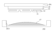
도 1a는 본 발명의 실시예 중 발광 장치(100)의 저면도로서, 명확하게 표시하기 위하여, 도 1a는 일부 층만 나타내었고, 또한 그 재료가 불투명이든, 투명 또는 반투명이든 막론하고 각 층마다 모두 실선으로 도시하였다(그러나, 도전층(1116)은 점선으로 표시하였으며, 이후에 상세히 설명한다). 도 1b는 도 1a의 I-I선 구간의 단면도이고, 도 1c는 도 1a의 Ⅱ-Ⅱ선 구간의 단면도이며, 도 1d는 도 1b의 A부분의 확대도이다. 도 1e는 도 1c의 B부분의 확대도이다. 간단히 표시하기 위하여, 도 1b 및 도 1c의 발광 구조(11)는 사각형으로만 표시하였으며, 상세한 구조는 도 1d 및 도 1e에서 설명하도록 하겠다.FIG. 1A is a bottom view of a
도 1a, 도 1b, 및 도 1d를 참조하면, 발광 장치(100)는 발광 구조(11), 투광체(12), 파장 전환체(13), 제1 반사층(14), 연장 전극(15A, 15B), 및 제2 반사층(17)을 포함한다. 발광 구조(11)는 패턴화 기판(110) 및 2개의 발광 본체(111A, 111B)를 포함한다. 패턴화 기판(patterned substrate)(110)은 실질적으로는 하나의 직사각형체로서, 상부 표면(1101), 상부 표면(1101)에 대향하는 하부 표면(1102), 및 상부 표면(1101)과 하부 표면(1102) 사이에서 연결되는 4개의 측면[제1 측면(1103), 제2 측면(1104), 제3 측면(1105) 및 제4 측면(1106)]을 포함한다. 하부 표면(1102)은 패턴화 표면으로, 규칙적이거나 또는 불규칙적으로 배열된 요철 구조를 갖는다. 투광체(12)는 상부 표면(1101), 4개의 측면(1103)~(1106), 및 일부 하부 표면(1102)을 피복한다.1A, 1B, and 1D, the
도 1d를 참조하면, 본 실시예에서, 발광 구조(11)는 패턴화 기판(110), 패턴화 기판(110)에 공동으로 형성되는 두 개의 발광 본체(111A, 111B), 두 개의 발광 본체(11A), (111B)가 서로 물리적으로 분리되도록 두 발광 본체(111A, 111B) 사이에 형성되는 채널(112)을 포함한다. 각각의 발광 본체(111A, 111B)는 제1형 반도체층(1111), 활성층(1112), 및 제2형 반도체층(1113)을 포함한다. 제1 절연층(1114)은 채널(112)에 형성되어 발광 본체(111A, 111B)의 제1형 반도체층(1111)을 피복함으로서 인접한 발광 본체(111A, 111B) 사이의 불필요한 회로 경로(단락)를 방지한다. 제2 절연층(1115)은 제1 절연층(1114)에 형성되어 발광 본체(111A, 111B)의 제2형 반도체층(1113)을 노출시킨다. 도전층(1116)은 제2 절연층(1115) 및 발광 본체(111A, 111B)를 노출시키는 제2형 반도체층(1113)에 형성된다. 또한, 제2 절연층(1115)은 제1 절연층(1114)의 측벽에 피복될 수 있다. 도전층(1116)은 일부 제2 절연층(1115)의 측벽을 피복하고 제1형 반도체층(1113)까지 연장된다. 제3 절연층(1117)은 도전층(1116)에 형성되어 발광 본체(111A, 111B)를 피복하고, 또한 일부 도전층(1116)을 노출시킨다. 제1 전극(1118) 및 제2 전극(1119)은 각각 발광 본체(111A) 및 발광 본체(111B)에 전기적으로 연결된다. 발광 본체(111A, 111B) 사이의 전기적인 연결은 이후에 설명하도록 한다. 옴 접촉층(1120)은 발광 장치(110)의 구동 전압을 저하시키기 위하여 제2형 반도체층(1113)과 도전층(1116) 사이에 선택적으로 형성될 수 있다. Referring to FIG. 1D, in this embodiment, the
명확하게 표시하기 위하여, 도 1a의 도전층(1116)은 점선으로 표시하였다. 도 1a, 도 1d 및 도 1e를 참조하면, 도전층(1116)은 제1 영역(1161), 제2 영역(1162)(도 1a의 사선 블록) 및 제3 영역(1163)을 구비한다. 제1 영역(1161)은 발광 본체(111A)에만 형성되고 제2 영역(1162)과 물리적으로 분리된다. 제2 영역(1162)은 제1 영역(1161)을 둘러싼다. 제2 영역(1162)은 발광 본체(111A)의 제1형 반도체층(1111)과 접촉되고, 또한 채널(112) 중의 제2 절연층(1115)에 더 형성되어 발광 본체(111B)의 제2형 반도체층(1113)까지 연장되며, 이에 따라 도전층(1116)은 발광 본체(111A)와 발광 본체(111B)에 직렬 연결된다(단면선의 위치로 인해, 이 연결 관계는 도 1d에 도시되지 않았다).For clarity, the
도 1a, 도 1d 및 도 1e를 참조하면, 복수의 공동(1110)이 제3 절연층(1117)에 형성되며, 또한 공동(1110)은 발광 본체(111A) 부위에만 형성되고 발광 본체(111B) 부위에는 형성되지 않는다. 제1 전극(1118)은 공동(1110)까지 연장될 수 있으며 또한 발광 본체(111A)상의 도전층(1116)의 제1 영역(1161)과 전기적인 연결을 형성한다. 이를 통하여 제1 전극(1118)과 발광 본체(111A)의 제2형 반도체층(1113)은 전기적인 연결을 형성한다. 도전층(1116)의 제3 영역(1163)은 발광 본체(111B)에만 형성된다. 제2 전극(1119)은 제3 절연층(1117)으로터 노출된 도전층(1116)의 제3 영역(1163)과 직접적으로 접촉된다. 도전층(1116)의 제3 영역(1163)은 발광 본체(111B)의 제1형 반도체층(1111)과 접촉된다. 본 실시예에서, 예를 들어, 제1 전극(1118)이 외부 전극의 정극과 전기적으로 연결되고, 제2 전극(1119)은 외부 전극의 부극과 전기적으로 연결될 경우, 전류는 순차적으로 공동(1110) 내부의 제1 전극(1118), 도전층(1116)의 제1 영역(1161), 발광 본체(111A)의 제2형 반도체층(1113), 발광 본체(111A)의 활성층(1112), 발광 본체(111A)의 제1형 반도체층(1111), 도전층(1116)의 제2 영역(1162), 발광 본체(111B)의 제2형 반도체층(1113), 발광 본체(111B)의 활성층(1112), 발광 본체(111B)의 제1형 반도체층(1111), 도전층(1116)의 제3 영역(1163)을 거쳐, 마지막으로 제2 전극(1119)에 이르게 되며, 따라서 발광 본체(111A)와 발광 본체(111B)는 서로 직렬 연결된다. 또한, 이상의 전체적인 설계를 종합해보면, 공동(1110)을 발광 본체(111B)에 형성하는 제조 공정을 감소시킬 수 있고, 또한 도전층(1116)을 발광 본체(111A, 111B)의 측벽에 피복하여 발광 장치(100)의 광 강도(루멘)를 증가시키며 발광 장치(100)의 전체적인 순방향 바이어스 전압(Vf)을 낮출 수 있다.1A, 1D, and 1E , a plurality of
본 실시예에서, 제1 전극(1118), 제2 전극(1119), 도전층(1116)의 재료는 금속일 수 있으며, 예를 들어 금(Au), 은(Ag), 구리(Cu), 크롬(Cr), 알루미늄(Al), 백금(Pt), 니켈(Ni), 티타늄(Ti), 주석(Sn) 또는 이들의 합금 또는 이들의 적층 조합일 수 있다. 제1 절연층(1114)은 단층 또는 다층일 수 있다. 제1 절연층(1114)이 단층일 경우, 재료는 산화물, 질화물, 또는 중합물(polymer)을 포함할 수 있고; 산화물은 산화알루미늄(Al2O3), 산화규소(SiO2), 이산화티타늄(TiO2), 오산화이탄탈(Tantal㎛ Pentoxide, Ta2O5) 또는 산화 알루미늄(AlOx)를 포함할 수 있으며; 질화물은 질화 알루미늄(AlN), 질화규소(SiNx)를 포함할 수 있고; 중합물은 폴리이미드(polyimide) 또는 벤조시클로부탄(benzocyclobutane, BCB)을 포함할 수 있다. 제1 절연층(1114)이 다층인 경우, 재료는 분산 브래그 반사경(Distributed Bragg Reflector)을 형성하도록 산화알루미늄(Al2O3), 산화규소(SiO2), 이산화티타늄(TiO2), 오산화이니오브(Nb2O5) 및 질화규소(SiNx)의 적층을 포함할 수 있다. 제2 절연층(1115) 및 제3 절연층(1117) 재료의 선택은 제1 절연층(1114)을 참고할 수 있다.In this embodiment, the material of the
도 1a 및 도 1c를 참조하면, 투광체(12)는 발광 구조(11)를 피복하며 또한 실질적으로는 직사각형체이므로, 도 1a에서 투광체(12)는 직사각형이다. 투광체(12)는 상부 표면(121), 상부 표면(121)에 대향하는 하부 표면(122), 및 상부 표면(121)과 하부 표면(122) 사이에 연결되는 4개의 측면[제1 측면(123), 제2 측면(124), 제3 측면(125) 및 제4 측면(126)]을 포함한다. 도 1a에서, 제1 측면(123)은 실질적으로 제3 측면(125)과 평행하면서 직사각형체의 장변이고; 제2 측면(124)과 제4 측면(126)은 서로 평행하면서 직사각형체의 단변이다. 제2 반사층(17)은 제1 측면(123) 및 제3 측면(125)을 피복하되, 단 제2 측면(124), 제4 측면(126), 상부 표면(121) 및 하부 표면(122)은 피복하지 않는다. 따라서 제2 반사층(17)은 발광 구조(11)의 제1 측면(1103) 및 제3 측면(1105)을 피복하고, 발광 구조(11)의 제2 측면(1104) 및 제4 측면(1106)은 피복하지 않는다. 1A and 1C, since the
도 1c를 참조하면, 제2 반사층(17)은 외표면(171) 및 내표면(172)을 구비하며, 외표면(171)은 실질적으로는 평면(도 1c에서 직선임)이고 또한 상부 표면(121)에 수직이다. 내표면(172)은 호형(弧形) 형상을 갖는다. 상세히 설명하면, 내표면(172)과 외표면(171) 사이의 거리(D1)는 투광체(12)의 상부 표면(121)으로부터 하부 표면(122)에 이르는 방향으로 점차 좁아지며, 또한 내표면(172)은 제1 반사층(14)까지 연신되고, 또한 외표면(171)과는 접촉하지 않는다. 이 밖에, 연장 전극(15A)과 제2 반사층(17)은 Z방향에서 서로 중첩된다.Referring to FIG. 1C , the second
제2 반사층(17)은 발광 구조(11)가 방출하는 광이 투광체(12)의 상부 표면(121) 및/또는 측면(124, 126)을 향하여 발광 장치(100)를 이탈하도록 반사한다. 또한, 제2 반사층(17)은 기질, 및 기질에 도핑된 복수의 반사 입자를 포함하는 혼합물이기 때문에, 발광 구조(11)가 방출하는 광은 제2 반사층(17)에서 반사될 수 있으며, 또한 그 반사형태는 확산 반사(diffuse reflection)이다. 기질은 절연재료이면서 또한 실리콘 기질(silicone-based) 또는 에폭시 기질(epoxy-based)을 포함하며; 반사 입자는 이산화티타늄, 이산화규소, 황산바륨, 또는 산화알루미늄을 포함할 수 있다. 제2 반사층(17)의 상이한 파장에 대한 반사율은 그 두께와 상관성이 있기 때문에, 제2 반사층(17)의 두께[즉 내표면(172)과 외표면(172) 사이의 최대 거리]는 50㎛~160㎛ 사이이다. 제2 반사층(17)의 두께가 50㎛ 미만인 경우, 파고값이 430~450nm인 광에 대한 반사율이 90% 미만일 수 있고; 파고값이 540~570nm인 광에 대한 반사율은 88% 미만일 수 있으며; 파고값이 620~670nm인 광에 대한 반사율은 80% 미만일 수 있다. 제2 반사층(17)의 두께가 약 160㎛인 경우, 파고값이 430~450nm인 광, 540~570nm인 광 및 620~670nm인 광에 대한 반사율이 모두 95% 이상이다. 그러나, 제2 반사층(17)의 두께가 160㎛보다 큰 경우, 발광 장치(100)의 Y방향 두께 및 제조원가가 증가하게 되어 그 응용성이 제한될 수 있다[예를 들어 핸드폰, 액정 디스플레이, 웨어러블 장치(시계, 밴드, 목걸이 등)]. 또 다른 실시예에서, 상이한 응용 상황에 따라, 제2 반사층(17)의 두께는 160㎛보다 크거나, 또는 50㎛~1000㎛ 사이일 수도 있다.The second
도 1b 및 도 1d를 참조하면, 제1 반사층(14)은 제3 절연층(1117)에 형성되며 또한 제1 부분(141), 제2 부분(142) 및 제3 부분(143)을 구비한다. 연장 전극(15A), (15B)은 제1 반사층(14)에 형성된다. 상세히 설명하면, 제1 반사층(14)의 제1 부분(141)은 일부 제1 전극(1118)만 피복하면서 또한 호형 단면을 구비하고; 제1 반사층(14)의 제2 부분(142)은 제1 전극(1118) 및 제2 전극(1119) 사이에 형성되면서 일부 제1 전극(1118) 및 일부 제2 전극(1119)을 피복하며; 제1 반사층(14)의 제3 부분(143)은 일부 제2 전극(1119)만 피복한다. 연장 전극(15A)은 제1 반사층(14)의 제1 부분(141) 및 제2 부분(142)만 피복하고, 연장 전극(15B)은 제1 반사층(14)의 제2 부분(142) 및 제3 부분(143)만 피복한다. 연장 전극(15A) 및 연장 전극(15B)은 각각 제1 전극(1118) 및 제2 전극(1119)과 접촉되면서 전기적인 연결을 형성한다. 연장 전극(15A)은 제2측 표면(124)과 함께 평면을 이루는 제1단(151); 제1 반사층(14)의 제2 부분(142)에 위치하면서 호형 단면을 갖는 제2단(152)을 구비한다. 연장 전극(15B)은 연장 전극(15A)과 유사한 구조를 갖는다. 도 1d에서, 제1 반사층(14)의 제2 부분(142)은 제3 절연층(1117)과 직접 접촉하면서 제1 전극(1118) 및 제2 전극(1119) 사이에 완전히 충전되고, 또한 제1 반사층(14)과 제3 절연층(1117) 사이에는 투광체(12)가 형성되어 있지 않다. 또 다른 실시예에서, 제조 과정에서, 투광체(12)는 제1 반사층(14)과 제3 절연층(1117) 사이에 형성될 수 있다.1B and 1D , the first
도 1b 및 도 1c를 참조하면, 파장 전환체(13)는 투광체(12) 내에 형성된다. 본 실시예에서, 파장 전환체(13)는 모체에 분산되는 복수의 파장전환 입자(131)를 포함한다. 파장 전환 입자(131)는 패턴화 기판(110)의 상부 표면(1101), 제1 측면(1103), 제2 측면(1104), 일부 제3 측면(1105) 및 일부 제4 측면(1106)을 피복한다. 일부 제3 측면(1105) 및 일부 제4 측면(1106)은 파장 전환 입자(131)가 피복되지 않는다. 선택적으로, 파장 전환체(13) 및/또는 투광체(12)는 확산 분말을 더 포함할 수 있다. 모체는 에폭시 수지(Epoxy), 실리콘(Silicone), 폴리이미드(PI), 벤조시클로부탄(BCB), 과불화시클로부탄(PFCB), Su8, 아크릴산수지(Acrylic Resin), 폴리메틸메타크릴레이트(PMMA), 폴리에틸렌테레프탈레이트(PET), 폴리카보네이트(PC), 또는 폴리에테르이미드(Polyetherimide)를 포함한다. 투광체(12)는 에폭시 수지(Epoxy), 실리콘(Silicone), 폴리이미드(PI), 벤조시클로부탄(BCB), 과불화시클로부탄(PFCB), Su8, 아크릴산수지(Acrylic Resin), 폴리메틸메타크릴레이트(PMMA), 폴리에틸렌테레프탈레이트(PET), 폴리카보네이트(PC), 또는 폴리에테르이미드(Polyetherimide)를 포함할 수 있다. 파장 전환체(13)의 모체와 투광체(12)의 재료가 동일한 경우, 전자현미경으로 조사하였을 때 그 사이의 경계면이 모호하여 불분명하거나, 또는 파장 전환체(13)의 모체와 투광체(12) 사이에 존재하는 경계면이 보이지 않는다면, 이는 즉 파장 전환 입자(131)가 투광체(12) 내에 분산된 것을 의미한다.1B and 1C , the
파장 전환 입자(131)는 5㎛~100㎛의 입자 크기를 가지면서 1종 또는 2종 이상의 종류의 무기 형광 분말(phosphor), 유기분자 형광색소(organic fluorescent clorant), 반도체 재료(semiconductor), 또는 상기 재료의 조합을 포함할 수 있다. 무기 형광 분말 재료는 황록색 형광 분말 또는 적색 형광 분말을 포함하되, 단 이에 한정되지 않는다. 황록색 형광 분말의 성분은 예를 들어 알루미늄산화물(YAG 또는 TAG), 규산염, 바나듐산염, 알칼리토금속 셀레늄화물, 또는 금속 질화물이다. 적색 형광 분말의 성분은 예를 들어 불화물(K2TiF6:Mn4 +, BK2SiF6:Mn4 + ), 규산염, 바나듐산염, 알칼리토금속 황화물, 금속질산화물, 또는 텅스텐 몰리브덴산염족 혼합물이다. 파장 전환 입자의 모체 중에서의 중량 백분 농도(w/w)는 50~70% 사이이다. 반도체 재료는 나노 크기의 결정체(nano crystal) 반도체 재료, 예를 들어 양자점(quant㎛-dot) 발광재료를 포함한다. 양자점 발광재료는 황화아연(ZnS), 셀레늄화아연(ZnSe), 텔루르화아연(ZnTe), 산화아연(ZnO), 황화카드뮴(CdS), 셀레늄화카드뮴(CdSe), 텔루르화카드뮴(CdTe), 질화갈륨(GaN), 인화갈륨(GaP), 셀레늄화갈륨(GaSe), 안티몬화갈륨(GaSb), 비화갈륨(GaAs), 질화알루미늄(AlN), 인화알루미늄(AlP), 비화알루미늄(AlAs), 인화인듐(InP), 비화인듐(InAs), 텔루륨(Te), 황화납(PbS), 안티몬화인듐(InSb), 텔루르화납(PbTe), 셀레늄화납(PbSe), 텔루르화안티몬(SbTe), 황화아연카드뮴셀레늄(ZnCdSeS), 황화구리인듐(CuInS), 세슘염화납(CsPbCl3), 세슘브롬화납(CsPbBr3), 및 세슘요오드화납(CsPbI3)으로 구성된 그룹에서 선택될 수 있다.The
확산 분말은 이산화티타늄, 산화지르코늄, 산화아연 또는 산화알루미늄을 포함하며, 발광 구조(11)가 방출하는 광을 분산시킬 수 있다. 확산 분말의 모체 중에서의 중량 백분 농도(w/w)는 0.1~0.5% 사이이고 또한 10nm~100nm 또는 10~50㎛의 입자 크기를 갖는다. 일 실시예에서, 확산 분말(또는 파장 전환 입자)의 모체 중에서의 중량 백분 농도는 열 중량 분석기(thermogravimetric analyzer; TGA)를 통해 측정할 수 있다. 간략하게 설명하면, 가열 과정에서, 모체가 온도가 점차 상승하여 특정 온도에 도달한 후 제거(증발 또는 열분해)될 수 있기 때문에, 확산 분말(또는 파장 전환 입자)이 잔류하게 된다. 측정 중량의 변화를 통해 모체와 확산 분말(또는 파장 전환 입자) 각자의 중량, 및 확산 분말의 모체 중에서의 중량 백분 농도를 획득할 수 있다. 또는, 모체와 확산 분말(또는 파장 전환 입자)의 총 중량을 먼저 측정한 다음, 용매를 이용하여 접착체를 제거하고, 마지막으로 확산 분말(또는 파장 전환 입자)의 중량을 측정하여, 확산 분말(또는 파장 전환 입자)의 모체 중에서의 중량 백분 농도를 구할 수 있다.The diffusion powder includes titanium dioxide, zirconium oxide, zinc oxide, or aluminum oxide, and may disperse light emitted by the
파장 전환 입자(131)는 발광 구조(11)가 방출하는 제1광을 흡수하여 제1광과 다른 주파수 스펙트럼의 제2광으로 전환할 수 있다. 제1광이 제2광과 혼합될 경우 제3광이 발생할 수 있다. 본 실시예에서, 제3광은 CIE1931 색 표시계 중 색점 좌표(x, y)를 가지며, 그 중, 0.27≤x≤0.285이고; 0.23≤y≤0.26이다. 또 다른 일 실시예에서, 제1광이 제2광과 혼합되어 제3광, 예를 들어 백색광이 발생할 수 있다. 파장 전환 입자의 중량 백분 농도 및 종류에 따라 발광 장치가 열안정 상태에서 갖는 백색광의 상대적 색온도(CCT)는 2200K~6500K(예를 들어 2200K, 2400K, 2700K, 3000K, 5700K, 6500K)이고, CIE1931 색 표시계 중 7개의 맥아담 편차 타원(MacAdam ellipse)의 범위에 포함될 수 있는 색점 좌표(x, y)를 가지며, 또한 80보다 크거나 또는 90보다 큰 연색성(CRI)을 갖는다. 또 다른 일 실시예에서, 제1광은 제2광과 혼합되어 자색광, 호박광, 녹색광, 황색광 또는 기타 백색광이 아닌 색광을 발생시킬 수 있다.The
도 1a~도 1c를 통해 알 수 있듯이, 투광체(12)의 제1 측면(123) 및 제3 측면(125)은 제2 반사층(17)에 의해 피복되고, 또한 하부 표면(122)은 제1 반사층(14) 및 연장 전극(15A), (15B)에 의해 피복된다. 따라서 발광 장치(100)는 실질적으로 3개의 출광면만 구비한다. 다시 말해, 발광 구조(11)가 방출하는 광은 투광체(12)의 상부 표면(121), 제2 측면(124) 및 제4 측면(126)을 직접 관통하여 발광 장치(100)를 이탈한다. 발광 구조(11)의 발광 각도(그 정의는 이후에 설명할 것이다)는 약 140도이며, 따라서 50% 이상의 광이 상부 표면(1101)[또는 투광체(12)의 상부 표면(121)]으로부터 외부로 방출되며, 또한 발광 구조(11)의 상부 표면(1101)은 발광 구조(11)의 주 출광면으로 정의된다. 발광 구조(11)와 발광 장치(100)의 출광 방향은 동일하며, 모두 Z축 방향으로부터 외부로 방출된다(발광 장치(100)를 이탈한다). 따라서, 발광 구조(11)의 주 출광면과 발광 장치(100)의 출광면은 실질적으로 평행하다.As can be seen from FIGS. 1A to 1C , the
도 2a~도 2c는 각각 본 발명의 또 다른 실시예 중 발광 장치(100'), (100"), (100'")의 단면도이다. 발광 장치(100'), (100"), (100'")는 발광 장치(100)와 유사한 구조를 갖는다. 그 중 동일한 부호 또는 기호에 대응되는 소자 또는 장치는 유사하거나 또는 동일한 소자 또는 장치이다. 도 1c, 도 2a~도 2c는 도 1a 중 Ⅱ-Ⅱ선 구간을 따른 단면도이다. 그리고 대응하는 평면도, I-I선 구간을 따르는 단면도는 도 1a, 도 1b, 및 도 1d를 참조할 수 있다. 2A to 2C are cross-sectional views of light emitting
도 2a를 참조하면, 제2 반사층(17')은 외표면(171') 및 내표면(172')을 구비한다. 외표면(171')은 실질적으로 평면(도 2a에서 직선임)이고 또한 상부 표면(121)에 수직이다. 내표면(172')은 호형 형상을 갖는다. 상세히 설명하면, 내표면(172')과 외표면(171') 사이의 거리(D1)는 투광체(12)의 상부 표면(121)으로부터 하부표면(122)으로의 방향을 따라 점차 축소되고, 또한 내표면(172')은 외표면(171')과 서로 만난다. Referring to FIG. 2A , the second
도 2b를 참조하면, 제2 반사층(17")은 외표면(171") 및 내표면(172")을 구비한다. 외표면(171")은 실질적으로 평면(도 2b에서 직선임)이고 또한 상부 표면(121)에 수직이다. 내표면(172")은 호형 형상을 갖는다. 상세히 설명하면, 내표면(172")과 외표면(171") 사이의 거리(D1)는 투광체(12)의 상부 표면(121)으로부터 하부표면(122)으로의 방향을 따라 점차 확대된다. Referring to Figure 2B, the second
도 2c를 참조하면, 제2 반사층(17'")은 외표면(171'") 및 내표면(172'")을 구비한다. 외표면(171'") 및 내표면(172'")은 실질적으로 모두 평면(도 2c에서 직선임)이고 또한 상부 표면(121)에 수직이다.Referring to Figure 2c, the second reflective layer 17'" has an outer surface 171'" and an inner surface 172'". The outer surface 171'" and the inner surface 172'" are It is substantially all planar (which is straight in FIG. 2C ) and is also perpendicular to the
도 2d는 본 발명의 또 다른 실시예 중 발광 장치(200)의 단면도이다. 발광 장치(200)는 발광 장치(100)와 유사한 구조를 갖는다. 그 중 동일한 부호 또는 기호에 대응되는 소자 또는 장치는 유사하거나 또는 동일한 소자 또는 장치이다. 본 실시예에서, 제2 반사층(27)은 금(Au), 은(Ag), 구리(Cu), 크롬(Cr), 알루미늄(Al), 백금(Pt), 니켈(Ni), 또는 로듐(Rh)과 같은 금속을 포함하며, 따라서 발광 구조(11)가 방출하는 광이 제2 반사층(27)에서 발생시키는 반사형태는 경면 반사(specular reflection)이다. 이밖에, 제2 반사층(27)이 금속이면서 또한 제2 반사층(27)의 두께가 50-200Å인 경우, 99%의 반사율을 즉시 달성할 수 있으며, 따라서, 발광 장치(200)의 Y 방향의 두께를 감소시킬 수 있다. 비교적 작은 크기는 발광 장치(200)의 응용성[예를 들어 핸드폰, 액정 디스플레이, 웨어러블 장치(시계, 밴드, 목걸이 등)]을 증가시키는데 도움이 된다. 제2 반사층(27)은 스퍼터(sputter), 전기도금 또는 화학도금 방식을 통해 투광체(12)에 형성될 수 있다. 선택적으로, 한 층의 점착층(미도시), 예를 들어 이산화규소를 첨가하면 제2 반사층(27)과 투광체(12) 사이에 상호간의 접착력을 증가시킬 수 있다. 또는 먼저 투광체(12)에 대해 표면 처리(예를 들어 헬륨가스, 산소가스 또는 질소가스의 플라즈마 처리)를 실시한 다음, 제2 반사층(27)을 직접 형성하며, 다시 말해, 제2 반사층(27)을 투광체(12)와 직접 접촉시켜 투광체(12)와 제2 반사층(27) 사이의 접착력을 증가시킬 수 있다.2D is a cross-sectional view of a
제2 반사층의 단면 형상은 제조 과정 중에 사용되는 커터 형상 및 크기에 의해 결정된다. 커터가 호형 단면을 갖는 경우, 제2 반사층은 호형 단면의 내표면을 구비하고(도 1c, 도 2a 및 도 2b 참조); 커터가 직선 단면을 갖는 경우, 즉 제2 반사층은 직선 단면의 내표면을 구비한다(도 2c, 도 2d 참조). 물론, 커터의 형상 및 크기는 호형의 곡률도 결정할 수 있다. 또한, 제2 반사층 내표면의 형상은 발광 장치의 휘도에 영향을 줄 수 있다. 일반적으로, 직선 단면에 비해, 호형 단면의 내표면을 갖는 제2 절연층은 비교적 많은 광이 발광 장치로부터 이탈되도록 할 수 있다. 또한, 도 2b의 발광 장치는 도 2a 또는 도 1c의 발광 장치에 비해 비교적 큰 발광 휘도를 갖는다[예를 들어 광속(루멘값)].The cross-sectional shape of the second reflective layer is determined by the cutter shape and size used during the manufacturing process. when the cutter has an arc-shaped cross-section, the second reflective layer has an inner surface of an arc-shaped cross-section (see Figs. 1C, 2A and 2B); If the cutter has a straight cross-section, ie the second reflective layer has an inner surface of a straight cross-section (see Figs. 2c, 2d). Of course, the shape and size of the cutter can also determine the curvature of the arc. In addition, the shape of the inner surface of the second reflective layer may affect the luminance of the light emitting device. In general, the second insulating layer having an inner surface of an arc-shaped cross-section as compared to a straight cross-section can allow relatively much light to escape from the light emitting device. In addition, the light emitting device of Fig. 2B has a relatively large light emitting luminance (for example, luminous flux (lumen value)) compared to the light emitting device of Fig. 2A or 1C.
도 1a를 참조하면, 제2 반사층(17)이 제1 측면(123) 및 제3 측면(125)에만 피복되므로, 발광 구조(11)에 의해 방출되어 제1 측면(123) 및 제3 측면(125)을 향하는 광은 제2 반사층(17)에 의해 반사될 수 있다. 그러나, 제2 측면(124) 및 제4 측면(126)을 향하는 광은 발광 장치(100)를 직접 이탈하게 된다. 따라서, 발광 장치(100)는 방향에 따라 상이한 발광 각도를 갖게 된다. 좀 더 구체적으로 설명하면, 도 1f는 발광 장치(100)의 측정 방식 설명도이다. 발광 장치(100)가 발광할 때, 고니어포토미터(Goniophotometer; AMA Optoelectronincs Inc, 모델명:LID-100CS)를 이용하여 원 P1 또는 원 P2 상의 각 점의 발광 강도를 측정하여 얻을 수 있다. 원 P1 또는 원 P2는 측정을 위해 정의된 가상원이다. 원 P1 상의 각 점에 대응되는 각도 및 발광 강도를 측정하여 기록하면 제1 배광 곡선도를 얻을 수 있고 제1 발광 각도를 도출할 수 있다. 마찬가지로, 원 P2 상의 각 점에 대응되는 각도 및 발광 강도를 측정하여 기록하면 제1 배광 곡선도를 얻을 수 있고 제1 발광 강도를 도출할 수 있다. 원 P1 및 원 P2와 관련된 상세한 설명은 대만 출원번호 105114875의 내용을 참고할 수 있다. 제1 발광 각도는 제2 발광 각도보다 클 수 있다. 일 실시예에서, 장변 방향(X 방향)의 제1 발광 각도는 130~150도 사이이고, 단변 방향(Y 방향)의 제2 발광 각도는 100~125도 사이이다. 또는 제1 발광 각도와 제2 발광 각도의 차이값 범위는 15도보다 크면서 15도~40도 사이에 개재된다. 여기서 설명하는 발광 각도는 휘도가 최대 휘도의 50%인 경우, 이때 포함되는 각도 범위를 즉 발광 각도로 정의한다. 발광 각도의 상세한 설명은 대만 출원안 104103105의 내용을 참고할 수 있다.Referring to FIG. 1A , since the second
도 1a 중의 두 발광 본체는 서로 직렬 연결된다. 기타 실시예에서, 발광 구조(11)는 하나의 발광 본체를 포함하거나 또는 3개 이상의 발광 본체가 서로 직렬연결, 병렬연결, 직렬 병렬 혼합 연결 또는 브리지형 연결될 수 있다. 발광 구조(11)에 복수의 발광 본체가 포함되는 경우, 복수의 발광 본체는 기판에 함께 형성되거나, 또는 복수의 발광 본체가 각자 하나의 기판을 구비하여, 하나의 캐리어 보드에 고정되거나, 또는 일부 발광 본체가 하나의 기판에 함께 형성되고, 또 다른 일부 발광 본체는 각자 하나의 기판을 구비하여, 이들이 다시 하나의 캐리어 보드에 함께 고정될 수 있다. 이밖에, 실시예 중의 2개의 발광 본체는 플립칩 구조이면서 또한 도전층을 투과하여 상호 전기적으로 연결되나, 2개의 발광 본체는 수평식 구조이면서 와이어 본딩 방식으로 상호 전기적으로 연결될 수도 있다.The two light emitting bodies in FIG. 1A are connected in series with each other. In other embodiments, the
상기 발광 본체가 이질 구조인 경우, 제1형 반도체층 및 제2형 반도체층은 예를 들어 클래딩층(cladding layer) 및/또는 구속층(confinement layer)으로서, 각각 전자, 정공을 제공하고 또한 활성층보다 큰 밴드 갭을 구비할 수 있으며, 이에 따라 전자, 정공이 활성층에서 결합되어 발광 확률을 높일 수 있다. 제1형 반도체층, 활성층, 및 제2형 반도체층은 Ⅲ-Ⅴ족 반도체 재료, 예를 들어 AlxInyGa(1-x-y)N 또는 AlxInyGa(1-x-y)P를 포함할 수 있으며, 그 중 0≤x, y≤1이고; (x+y)≤1이다. 활성층의 재료에 따라, 발광 본체는 하나의 파고값(peak wavelength) 또는 주 파장(dominant wavelength)이 610nm 및 650nm 사이에 개재되는 적색광, 파고값 또는 주 파장이 530nm 및 570nm 사이에 개재되는 녹색광, 파고값 또는 주 파장이 450nm 및 490nm 사이에 개재되는 청색광, 파고값 또는 주 파장이 400nm~440nm 사이인 자색광, 또는 파고값이 200nm~400nm 사이인 자외선광을 방출할 수 있다.When the light emitting body has a heterogeneous structure, the
도 3a~도 3g는 각각 본 발명의 일 실시예 중 발광 장치의 제조 흐름 단면도이고, 도 4a~4G는 각각 도 3a~3G의 평면도이다. 도 3a~3G는 각각 도 4a~4G 중 W-W선의 단면도이다. 간결하게 하기 위하여, 이후 묘사되는 발광 구조(11)는 도면에서 직사각형만 예로 들었으나, 평면도에서, 기타 형상, 예를 들어 정사각형, 사다리형, 평행사변형, 마름모형, 삼각형, 오각형, 육각형, 원형 역시 본 발명의 실시예에 응용될 수 있다. 이밖에, 명확히 표시하기 위하여, 각각의 구조들은 불투명, 투명 또는 반투명을 막론하고 모두 실선으로 도시하였다. 3A to 3G are cross-sectional views illustrating a manufacturing flow of a light emitting device according to an embodiment of the present invention, and FIGS. 4A to 4G are plan views of FIGS. 3A to 3G, respectively. 3A to 3G are cross-sectional views taken along line W-W in FIGS. 4A to 4G, respectively. For the sake of brevity, the
도 3a 및 도 4a를 참조하면, 캐리어 보드(22), 캐리어 보드(22)에 부착되는 접착재(21), 및 접착재(21)에 설치되는 복수의 발광 구조(11)를 제공한다. 본 실시예에서, 발광 구조(11)는 제1 전극(1118) 및 제2 전극(1119)의 측면으로 접착재(21)에 부착된다. 도 4a 중 발광 구조(11)의 수량 및 배열 방식은 단지 예시적인 것으로 이에 한정되지 않는다.Referring to FIGS. 3A and 4A , a
도 3b 및 도 4b를 참조하면, 복수의 파장 전환 입자(131)를 함유한 투명체로 발광 구조(11)를 완전히 피복한다. 투명체는 디스펜싱(dispensing), 코팅(coating), 스프레이 코팅(spray), 인쇄(screen printing) 등 방식을 이용하여 발광 구조(11)에 형성될 수 있다. 이후, 투명체를 경화시켜 투광체(12)를 형성한다. 투명체가 스프레이 코팅(spraying) 또는 디스펜싱(dispensing) 방식으로 발광 구조(11)에 형성되는 경우, 투명체는 전체 영역의 상이한 위치에 상이한 높이(Z 방향)를 가질 수 있다. 경화 후, 투명체는 투광체(12)로 경화되고, 투광체(12)는 상이한 위치에 역시 상이한 높이를 가질 수 있다. 따라서 먼저 물리적인 제거 단계를 통해 투광체(12)를 평탄화하여, 투광체(12)의 상부 표면(127)이 실질적으로 평탄해지도록 할 수 있다. "물리적인 제거 단계" 및 "실질적으로 평탄하다"는 정의는 이후에 상세히 설명하도록 하겠다.Referring to FIGS. 3B and 4B , the
또한, 본 실시예에서, 중력에 의해 경화 과정 중, 파장 전환 입자(131)가 자연적으로 침전될 수 있기 때문에, 대부분의 파장 전환 입자(131)가 발광 구조(11)와 접촉하게 되고, 파장 전환 입자(131) 중 일부만 발광 구조(11)의 측면에 부착될 수 있다(상세한 구조는 도 1b 및 도 1c의 관련 설명 참조). 기타 실시예에서, 경화 온도 및 시간을 제어하여 투광체(12) 중 파장 전환 입자(131)의 분포 상태를 제어할 수 있다. 예를 들어, 파장 전환 입자(131)가 저부까지 침전되지 않았고 또한 투명체가 이미 완전히 경화된 경우, 파장 전환 입자(131)는 투광체(12)에 부유하면서 발광 구조(11)와 접촉하지 않게 된다. 또는, 투명체에 침전방지제(예를 들어 이산화규소)를 첨가하여도, 파장 전환 입자(131)가 경화 과정에서 저부까지 침전되는 것을 방지할 수 있어, 파장 전환 입자(131)가 투명체에 고르게 분산될 수 있다.In addition, in this embodiment, most of the
또 다른 일 실시예에서, 복수의 파장 전환 입자(131)를 함유한 투명체는 먼저 파장 전환편을 형성한 다음, 발광 구조(11)에 부착될 수 있다. 부착은 상부 몰드(미도시) 및 하부 몰드(미도시)의 밀착 결합을 통해, 파장 전환편을 동시에 가열 및 가압하여 파장 전환편이 발광 구조(11)와 긴밀히 접합되도록 연화시키는 방식이다. 이밖에, 상부 몰드 및 하부 몰드는 매우 인접해 있나, 파장 전환편이 아직 발광 구조(11)와 접촉하지 않았을 때 공기를 빼면, 파장 전환편과 발광 구조(11) 사이의 기포를 감소시켜, 파장 전환편과 발광 구조(11) 사이의 접착력을 높일 수 있다.In another embodiment, the transparent body containing the plurality of
도 3c, 도 3d 및 도 4c, 도 4d를 참조하면, 커터(23)를 제공하여 X 방향의 절단선(L)을 따라 절단하는 단계를 실시하여 복수의 그루브(231)를 투광체(12)에 형성한다. 그루브(231)의 형상은 커터(23)의 형상에 대응한다. 예를 들어, 본 실시예에서, 커터(23)는 호형 단면을 구비하며, 따라서 그루브(231) 역시 호형 단면을 구비한다. 이밖에, 투광체(12) 역시 호형 단면을 구비하고, 또한 호형 단면은 하부 표면(122)에 비교적 가깝고 또한 발광 구조(11)를 둘러싼다. 또한, 호형 단면과 발광 구조(11)의 거리는 Z 방향을 따라 갈수록 좁아진다.Referring to FIGS. 3C, 3D, and 4C and 4D , a
도 3e 및 도 4e를 참조하면, 복수의 반사 입자(미도시)를 기질 중에 혼입하여 미경화 상태의 접착층을 형성한다(접착층의 색상은 혼입된 반사 입자에 의해 결정될 수 있으며, 통상적인 색상은 백색이다). 이어서, 접착층으로 투광체(12) 및 그루브(231)를 피복하고(바람직하게는, 그루브(2341)가 접착제층에 의해 완전히 피복되거나 근소한 일부 영역만 피복되지 않거나 또는 기포가 잔류되도록 한다); 접착층을 완전히 경화시켜 제2 반사층(17)을 형성한다. 제2 반사층(17)의 높이는 투광체(12)의 높이보다 높다. 제2 반사층(17)은 디스펜싱(dispensing), 코팅(coating), 스프레이 코팅(spray), 인쇄(screen printing) 등 방식을 이용하여 형성될 수 있다. 유사하게, 제2 반사층(17)은 반사편을 미리 형성한 다음 투광체(12)에 접합시킨 것일 수도 있다. 접합에 관한 묘사는 전술한 관련 단락을 참고할 수 있다.Referring to FIGS. 3E and 4E , a plurality of reflective particles (not shown) are incorporated in a substrate to form an adhesive layer in an uncured state (the color of the adhesive layer may be determined by the incorporated reflective particles, and a typical color is white am). Then, the
도 3f 및 도 4f를 참조하면, 물리적인 제거 단계(연마 또는 절삭)를 이용하여 제2 반사층(17)의 일부를 제거함으로써 투광체(12)를 노출시킨다. 본 실시예에서, 접착층은 스프레이(spraying) 또는 디스펜싱(dispensing) 방식으로 형성되므로, 접착층은 전체 영역의 상이한 위치에 상이한 높이(Z 방향)를 가질 수 있다(도 3E 참조). 경화 후, 접착층은 제2 반사층(17)으로 경화되고, 또한 제2 반사층(17)은 상이한 위치에 역시 상이한 높이를 가진다. 물리적인 제거 단계에서, 일부 제2 반사층(17)은 투광체(12)가 노출될 때까지 먼저 제거된다. 또한, 계속 제거 단계를 실시할 수 있으며, 따라서 제2 반사층(17) 및 투광체(12)가 동시에 제거될 수 있다. 이에 따라, 상기 과정을 이용하여 투광체(12)의 높이를 감소시킬 수 있다. 도 3F 중 투광체(12)의 높이는 도 3E의 투광체(12)의 높이보다 낮거나 같을 수 있다. 이밖에, 제2 반사층(17)은 투광체(12)의 상부표면(127)과 실질적으로 공면(共面)인 상부표면(173)을 가지며, 또한 상부 표면(127), (173)은 실질적으로 평탄하다.3F and 4F , the
"실질적으로 평탄하다"는 여기에서 전자식 현미경으로 60~100배 확대한 배율하에 발광 장치(100)를 관찰하여, 그 상부 표면(127), (173)이 대체로 격렬한 높낮이 기복이 없는 평면임을 이르는 것으로 정의된다. 그러나, 발광 장치(100)를 전자식 현미경으로 400배 확대한 배율하에 분석하는 경우, 또는 표면 윤곽 조도기(alpha stepfilm thickness measuring instrument) 또는 원자력 현미경(auomicforce microscope; AFM)으로 측정할 경우, 투광체(12)와 제2 반사층(17)은 거친 상부 표면(127), (173)을 가질 가능성이 있다. 이밖에, 본 실시예에서, 투광체(12)는 경도(Shore D)가 30~90인 실리콘이고, 제2 반사층(17)의 기질은 경도(Shore D)가 10~70인 실리콘이다. 투광체(12)의 경도와 제2 반사층(17)의 기질의 경도차가 30미만이므로, 물리적인 제거 단계를 거친 후, 투광체(12) 상부 표면(127)의 최대 조도(거칠기)차(Ra1)는 제2 반사층(17) 상부 표면(173)의 최대 조도차(Ra2)보다 약간 크거나, 같거나, 또는 약간 작을 수 있다. 표면 윤곽 조도기(alpha stepfilm thickness measuring instrument)를 통해 투광체(12)의 상부 표면(127)을 측정하여, 0.5mm의 측정 길이 중, 투광체(12)의 상부 표면(127) 중 최고점과 최저점의 차이값(최대 조도차로 정의함)은 Ra1이고; 마찬가지로, 제2 반사층(17)의 상부 표면(173)을 측정 시, 50㎛의 측정 길이 중, 제2 반사층(17)의 상부 표면 중 최고점과 최저점의 차이값은 Ra2이며; 2㎛≤Ra1≤15㎛이고; 2㎛≤Ra2≤15㎛이며; 0≤│Ra1-Ra2│≤13㎛이다."Substantially flat" refers to observing the
물리적인 제거 단계는 기계 절단기를 이용하여 실시된다. 기계 절단기의 재료는 고탄소강, 금강석, 세라믹 또는 산화붕소를 포함할 수 있다. 제거 과정에서, 물만 투입하여(연마액(slurry) 또는 화학용액을 투입할 필요 없다) 절단기와 제2 반사층(17) 사이의 마찰로 인해 상승한 온도를 낮출 수 있으며, 또한 이를 통해 이미 제거된 제2 반사층(17)과 이미 제거된 투광층(12)을 세척할 수 있다. 이뿐만 아니라, 사용되는 절단기의 경도가 제2 반사층(17) 및 투광체(12)보다 큰 경우, 다수의 스크래치(미도시)가 반사 절연층(12)과 투광체(12)에 형성될 수 있으며, 이는 광학현미경을 통해 관찰할 수 있다. 그러나 일 실시예에서, 절단 파라미터(예를 들어 절단 속도 또는 절단기의 재료)를 조정하면, 광학 현미경을 통해 스크래치를 관찰하지 못할 가능성이 있다.The physical removal step is performed using a mechanical cutter. The material of the machine cutter may include high carbon steel, granite, ceramic or boron oxide. In the removal process, only water (no need to add abrasive or chemical solution) can lower the temperature that has risen due to friction between the cutter and the second
도 3f, 도 4g 및 도 5a~도 5c를 참조하면, 절단선 L(X 방향 및 Y 방향)을 따라 절단 단계를 실시하여 복수의 서로 독립된 발광 장치(300)를 형성한다. 이어서, 접착재(21)를 가열하거나 또는 UV광을 접착재(21)에 조사하여 발광 구조(11) 및 투광체(12)를 접착재(21)로부터 분리시킨다. 선택적으로, 제1 반사층(14) 및 연장 전극(15A, 15B)를 더 형성할 수 있으며, 이에 대한 상세한 묘사는 기타 관련 단락을 참고할 수 있다.3F, 4G, and 5A to 5C, a plurality of independent
도 3c 및 도 4c를 참조하면, 절단 위치가 다름에 따라, 투광체(12)와 발광 구조(11)의 상대 위치를 변경할 수 있으며, 이는 즉 제1 측면(1103) 및 제1 측면(123)의 거리, 및 제3 측면(1105) 및 제3 측면(125)의 거리를 변경하는 것을 의미한다(도 1a 참조). 이어서, 도 3f 및 도 4f를 참조하면, 제2 반사층(17)을 그루브(231)에 충전하고 투광체(12)의 측면을 피복한다. 발광 구조(11)가 방출하는 광이 제2 반사층(17)을 향하는 경우, 광은 투광체(12)와 제2 반사층(17)의 경계면[예를 들어 도 1c에 도시된 바와 같이, 투광체(12)의 제1 측면(123) 및 제2 반사층(17)의 내표면(172)] 또는 제2 반사층(17) 내에서 반사 및/또는 굴절이 발생할 수 있다. 이상을 종합해보면, 도 3c의 제조 과정을 통해 미리 설정된 발광 장치의 파 필드(far field) 광 타입 및 발광 휘도[예를 들어 광속(루멘값)]를 얻을 수 있다.Referring to FIGS. 3C and 4C , according to the different cutting positions, the relative positions of the
도 6a~도 6b는 본 발명의 또 다른 일 실시예 중 제2 반사층(17)을 형성하는 단면도이다. 절단 단계가 완료된 후(도 3d 참조), 상부 몰드(251) 및 하부 몰드(252)를 제공하여, 캐리어 보드(22)를 상부 몰드(251)에 고정시키고 하부 몰드(252)의 오목홈(2521)에 경화되지 않은 상태의 접착층을 충전한다(접착층은 기질과 반사 입자를 포함하고, 접착층의 색상은 혼입된 반사입자에 의해 결정될 수 있으며, 통상적인 색상은 백색이다). 상하 몰드를 서로 근접시켜 압축 성형 단계(compression molding)를 실시하며, 이를 통해 접착층으로 투광체(12)를 피복하고 그루브(231) 안에 완전히 충전한다. 열처리 단계를 거쳐 접착층을 완전히 경화시켜 제2 반사층(17)을 형성한다. 본 실시예에서는 몰드를 통해 제2 반사층(17)을 형성하므로, 투광체(12) 상의 제2 반사층(17)은 상이한 위치에 동일한 높이를 지닌다. 이어서, 후속되는 동작은 도 3F~3G의 설명을 참고할 수 있다.6A to 6B are cross-sectional views of forming the second
도 7a~도 7g는 각각 본 발명의 또 다른 일 실시예 중 발광 장치(400)의 제조 흐름 단면도이다. 관련된 평면도는 도 4a~도 4g를 참고할 수 있다.7A to 7G are cross-sectional views showing a manufacturing flow of a
도 7a를 참조하면, 캐리어 보드(22), 캐리어 보드(22)에 접착되는 접착재(21), 및 접착재(21)에 설치되는 복수의 발광 구조(11)를 제공한다. 본 실시예에서, 발광 구조(11)는 전극(1118, 1119) 측이 접착재(21)에 부착된다. 이밖에, 캐리어 보드(22)는 상부 몰드(251)에 고정되고, 발광 구조(11)는 기판(110) 측이 하부몰드(252)를 향한다. 하부 몰드(252)의 오목홈(2521)에 복수의 파장 전환 입자(131)를 함유한 투명체를 충전한다. 이어서, 압축 성형 단계(compression molding)를 실시하며, 이를 통해 투명체는 발광 구조(11)를 완전히 피복할 수 있다. 중력의 영향으로 인하여, 투명체를 경화시키는 과정에서, 파장 전환 입자(131)가 하부 몰드(252)의 저부로 침전될 수 있기 때문에, 완전히 경화시켜 투광체(12)를 형성 시, 파장 전환 입자(131)는 투광체(12)의 상부 표면(121)에 집중될 수 있다. 기타 실시예에서, 경화 시간 및 경화 온도를 제어하여, 파장 전환 입자(131)가 하부몰드(252)의 저부로 아직 침전되지 않았을 때 투명체를 완전히 경화시켜 투광체(12)를 형성할 수 있다. 또는, 투명체에 침전 방지제를 첨가하여 경화 과정에서 파장 전환 입자(131)의 침전을 방지할 수 있다.Referring to FIG. 7A , a
도 7b~도 7d를 참조하면, 캐리어 보드(27)에 부착되는 접착재(26)를 제공한다. 도 7b의 구조를 투광체(12)로부터 접착재(26)에 부착한 후, 접착재(21)를 가열하거나 또는 UV광을 접착재(21)에 조사하여, 발광 구조(11) 및 투광체(12)를 접착재(21)로부터 분리시키고[접착재(21) 및 캐리어 보드(22)는 도 7c에 도시되지 않았음], 전극(1118, 1119)을 노출시킨다[도면의 시점 관계로 인해, 전극(1119)은 도면 중 표시되지 않았음]. 전극층(211)을 전극(1118, 1119)에 형성한다. 전극층(212)은 각각 단일한 발광 구조(11)의 전극(1118, 1119)에 형성되거나, 또는 전극층(211)은 발광 구조의 전극(1118) 및 발광 구조에 인접한 전극(1119)에 형성될 수 있다. 이에 따라, 인접한 발광 구조는 서로 직렬 연결된다(미도시), 또한, 커터(23)를 제공하여 절단선 L을 따라 절단 동작을 함으로써 복수의 그루브(231)를 투광체(12)에 형성한다. 그루브(231)의 형상은 커터(23)의 형상에 대응한다. 예를 들어, 본 실시예에서, 커터(23)는 호형 단면을 가지므로, 그루브(231) 역시 호형 단면을 가진다.7B to 7D , an adhesive 26 attached to the
도 7e 및 도 7f를 참조하면, 유사하게, 캐리어 보드(27)를 상부 몰드(251)에 고정시키고 하부 몰드(252)의 오목홈(2521)에 경화되지 않은 상태의 접착층을 충전한다. 압축 성형 단계를 실시하여, 경화되지 않은 상태의 접착층을 투광체(12), 전극층(211)에 피복하고 그루브(231)에 완전히 충전한 후, 열처리 단계를 거쳐 접착층을 완전히 경화시킴으로써 제2 반사층(17)을 형성한다. 본 실시예에서는 금형을 통해 제2 반사층(17)을 형성하기 때문에, 전극층(211)상의 제2 반사층(17)은 상이한 위치에서 동일한 높이를 갖는다. 이밖에, 제2 반사층(17)의 높이는 투광체(12)의 높이보다 높다.7E and 7F , similarly, the
도 7g를 참조하면, 물리적 제거 단계를 이용하여 제2 반사층(17)의 일부를 제거함으로써 전극층(211)을 노출시키고, 또한 다시 제거 단계를 계속 실시한다. 따라서 제2 반사층(17) 및 전극층(211)이 동시에 제거될 수 있으며, 이에 따라, 상기 공정을 이용하여 전극층(211)의 높이를 감소시킬 수 있다. 도 7g 중 전극층(211)의 높이는 도 7F의 전극층(211)의 높이보다 낮거나 또는 같을 수 있다. 제2 반사층(17)은 전극층(211)의 상부 표면(2111)과 실질적으로 공면인 상부 표면(173)을 갖는다. 본 실시예에서, 물리적인 제거 단계를 거친 후, 전극층(211)의 상부 표면(2111)의 최대 조도차(Ra3)는 제2 반사층(17) 상부 표면(173)의 최대 조도차(Ra4)보다 약간 크거나, 같거나, 또는 약간 작을 수 있다. 표면 윤곽 조도기(alpha stepfilm thickness measuring instrument)를 통해 전극층(211)의 상부 표면(2211)을 측정하여, 50mm의 측정 길이 중, 전극층(211)의 상부 표면(127) 중 최고점과 최저점의 차이값(최대 조도차로 정의함)은 Ra3이고; 마찬가지로, 제2 반사층(17)의 상부 표면(173)을 측정 시, 50㎛의 측정 길이 중, 제2 반사층(17)의 상부 표면 중 최고점과 최저점의 차이값은 Ra4이며; 2㎛≤Ra3≤15㎛이고; 2㎛≤Ra4≤15㎛이며; 0≤│Ra4-Ra3│≤13㎛이다.Referring to FIG. 7G , the
도 7g를 참조하면, 절단선 L을 따라 절단을 실시하는 단계로 복수의 서로 독립된 도 8a~도 8c에 도시된 바와 같은 발광 장치(400)를 형성한다. 접착재(26)를 가열하거나 또는 UV광을 접착재(26)에 조사하여, 발광 구조(11) 및 투광체(12)를 접착재(26)로부터 분리시킨다. 도 5a~도 5c의 발광 구조(300)와 다른 점은, 도 8A~8C 중 발광 구조(400)의 투광체(12)의 호형 단면이 발광 구조(11)를 둘러싸지 않고 투광체(12)의 상부 표면(121)에 인접하다는데 있다.Referring to FIG. 7G , a plurality of independent
접착재(21), (26) 및 캐리어 보드(22), (27)는 제작 과정에서 사용 시 발광 구조 또는 발광 장치를 고정시키기 위한 것이다. 접착재(21), (26)는 블루테이프, 방열플레이트/페이스트, 광분해 테이프(UV release tape) 또는 폴리에틸렌 테레프탈레이트(PET)를 포함한다. 캐리어 보드(22), (27)는 접착재(21), (26)를 지지하도록 유리 또는 사파이어를 포함한다.The
도 9a~도 9e는 본 발명의 또 다른 일 실시예 중 발광 장치(500)의 제조 흐름 평면도이다. 관련 단면도는 기타 부분을 참고할 수 있다.9A to 9E are plan views illustrating a manufacturing flow of a
도 9a 및 도 9b를 참조하면, 커터(미도시)가 X 방향과 Y 방향의 절단선 L을 따라 절단을 실시하는 단계로 복수의 그루브(231)를 투광체(12)에 형성한다.Referring to FIGS. 9A and 9B , a plurality of
도 9c를 참조하면, 제2 반사층(17)을 형성하여 투광체(12)를 피복하고 그루브(231)에 완전히 충전한다. 제2 반사층(17)의 형성 방식은 전술한 관련 단락을 참고할 수 있다.Referring to FIG. 9C , the second
도 9d를 참조하면, 물리적인 제거 단계를 이용하여 일부 제2 반사층(17)을 제거함으로써 투광체(12)를 노출시킨다. 기타 관련 설명은 도 4F의 설명을 참고할 수 있으므로, 여기서는 중복 설명을 생략한다.Referring to FIG. 9D , the
도 9e를 참조하면, 절단선 L(X 방향 및 Y 방향)을 따라 절단 단계를 실시하여 도 10a~도 10d에 도시된 바와 같은 복수의 서로 독립된 발광 장치(500)를 형성한다. 도 10a 및 도 10b를 참조하면, 제2 반사층(17)이 투광체(12)의 4개의 측면을 피복하고, 하부 표면(122) 역시 제1 반사층(14) 및 연장 전극(15A), (15B)에 의해 피복된 경우, 발광 장치(500)는 실질적으로 하나의 출광면만 구비한다. 도 10C 및 도 10d를 참조하면, 제2 반사층(17)이 투광체(12)의 3개의 측면을 피복하고, 하부 표면(122) 역시 제1 반사층(14) 및 연장 전극(15A), (15B)에 의해 피복된 경우, 발광 장치(500)는 실질적으로 2개의 출광면만 구비한다. 유사하게, 절단 위치가 다르면, 투광체(12)와 발광 구조(11)의 상대 위치가 변경되는 이외에, 다른 형식의 발광 장치를 더 형성할 수 있어, 미리 설정된 파필드 광형 및 발광 휘도[예를 들어 광속(루멘값)]를 획득하여 상이한 응용 수요를 만족시킬 수 있다.Referring to FIG. 9E , a plurality of independent
마찬가지로, 도 11a 및 도 11b에 도시된 바와 같이, 도 4f의 구조에서, 투광체(12)와 제2 반사층(17)의 경계면인 절단선(L)을 따라 절단하면 제2 반사층(17)이 투광체(12)의 일 측면만 피복하는 발광 장치(600)를 획득할 수 있다(도 11c 참조). 일 실시예에서, 제2 반사층(17)이 투광체(12)의 일 측면을 피복하고, 하부 표면(122) 역시 제1 반사층(14) 및 연장 전극(15A), (15B)에 의해 피복되는 경우, 발광 장치(600)는 실질적으로 4개의 출광면만 구비한다. 도 1a의 발광 장치(100)와 비교하여, 발광 장치(600)는 비교적 큰 발광 휘도[예를 들어 광속(루멘값)]를 더 구비한다.Similarly, as shown in FIGS. 11A and 11B , in the structure of FIG. 4F , when cut along the cutting line L, which is the interface between the light transmitting
도 12a는 본 발명의 일 실시예 중 발광 장치(700)의 평면도로서, 명확히 표시하기 위하여, 본 도면에서는 모든 소자를 도시하지 않았으며, 또한 각 층마다 불투명, 투명 또는 반투명을 막론하고 모두 실선으로 도시하였다. 도 12b는 도 12a의 I-I 선 구간의 단면도이다. 간단히 표시하기 위하여, 도 12a 및 도 12b의 발광 구조(11)는 직사각형만 예를 들었으나, 평면도에서, 정사각형, 사다리형, 평행사변형, 마름모형, 삼각형, 오각형, 육각형, 원형과 같은 기타 형상 역시 본 발명의 실시예에 응용될 수 있다. 도 12a 및 도 12b는 평면도 및 한 방향에서의 단면도만 도시한 것이다. 기타 관련 도면 시점 및 발광 구조(11)의 구조는 본 명세서 중 대응되는 단락 및 도면을 참고할 수 있다.12A is a plan view of a
도 12a 및 도 12b를 참조하면, 발광 장치(700)는 발광 구조(11), 파장 전환체(13), 투광체(12), 제1 반사층(14), 연장 전극(15A) 및 제2 반사층(17)을 포함한다. 발광 구조(11)는 상부 표면(1101), 상부 표면(110)에 대향하는 하부 표면(1102), 및 상부 표면(1101)과 하부 표면(1102) 사이에 연결되는 4개의 측면[제1 측면(1103), 제2 측면(1104), 제3 측면(1105) 및 제4 측면(1106)]을 포함한다. 파장 전환체(13)는 상부 표면(1101), 4개의 측면(1103)~(1106), 및 일부 하부 표면(1102)을 피복한다. 유사하게, 투광체(12)는 파장 전환체를 피복하며, 즉 다시 말해 투광체(12)는 파장 전환체(13)의 상부 표면 및 4개의 측면을 피복한다. 투광체(12)는 상부 표면(121), 상부 표면(121)에 대향하는 하부 표면(122), 및 상부 표면(121)과 하부 표면(122) 사이에 연결되는 4개의 측면[제1 측면(123), 제2 측면(124), 제3 측면(125) 및 제4 측면(126)]을 포함한다. 제2 반사층(17)은 상부 표면(121), 제1 측면(123), 제2 측면(124) 및 제4 측면(126)을 피복하되, 제3 측면(125) 및 하부 표면(122)은 피복하지 않는다. 다시 말해, 제2 반사층(17)은 발광 구조(11)의 제1 측면(1103), 제2 측면(1104) 및 제4 측면(1106)을 피복하나, 제3 측면(1105)은 피복하지 않는다.12A and 12B , the
도 12a 및 도 12b를 참조하면, 발광 구조(11)의 발광 각도는 약 140도이며, 따라서 50% 이상의 광이 상부 표면(1101)을 통해 외부로 방출될 수 있으며, 또한 발광 구조(11)의 상부 표면(1101)은 발광 구조(11)의 주 출광면으로 정의된다. 발광 구조(11)의 상부 표면(1101) 및 3개의 측면(1103, 1104, 1106)이 제2 반사층(17)에 의해 피복되고, 또한 하부 표면(1102)이 제1 반사층(14)에 의해 피복되므로, 발광 구조(11)가 방출하는 광은 제2 반사층(17) 또는/및 제1 반사층(14)을 통해 반사되어 제3 측면(1105) 및 투광체(12)의 제3 측면(125)을 경유하여 발광 장치(700)를 이탈하게 된다. 다시 말해, 발광 구조(11)와 발광 장치(700)의 출광 방향은 상이하여, 발광 구조(11)의 복수의 광선은 Z축 방향을 따라 외부로 사출되고[단 발광창치(700)는 이탈하지 않는다], 발광 장치(700)의 복수의 광선은 Y축 방향을 따라 외부로 사출된다[발광 장치(700)를 이탈한다]. 따라서, 발광 구조(11)의 주 출광면과 발광 장치(700)의 출광면은 실질적으로 수직이다.12A and 12B , the light emitting angle of the
이밖에, 도 12b에서, 비록 제2 반사층(17)의 하부 표면(174)은 평면이고 또한 제2 반사층(17)의 상부 표면(173)에 평행하나, 본 발명은 결코 이에 한정되지 않으며, 광을 발광 장치(700)로부터 추출하는데 도움이되는 광학 설계는 어떤 것이든 모두 제2 반사층(17)에 응용될 수 있다. 예를 들어, 투광체(12)의 상부 표면(121)[제2 반사층(17)의 하부 표면(174)을 개변할 수 있다]의 형상을 변경하여 발광 구조(11)의 광이 제3측 표면(1105)을 향하도록 유도함으로써 발광 구조(700)를 이탈하도록 할 수 있다. 관련 구조와 제작 과정은 뒤에서 설명할 것이다.Besides, in FIG. 12B , although the
발광 장치(700)는 0.3mm(≤0.3mm)를 초과하지 않는 높이(H0)를 가지며, 비교적 얇은 높이는 발광 장치(700)의 응용 분야[예를 들어 핸드폰, 액정 디스플레이, 웨어러블 장치(시계, 밴드, 목걸이 등)]를 넓히는데 도움이 된다. 상기한 바와 같이, 발광 구조(11)의 주 출광면이 발광 장치(700)의 출광면과 다르므로, 즉 발광 구조(11)와 발광 장치(700)가 상이한 출광 방향을 가지므로, 발광 구조(11)의 주 출광면적(XY 평면)을 증가시켜도, 발광 장치(700)의 전체 높이(Z 방향)가 증가하지 않는다. 발광 구조(11)의 출광량이 높아지므로, 발광 장치(700)의 전체적인 광속 역시 따라서 높아지나, 단 발광 장치(700)의 전체 높이는 증가하지 않아, 발광 장치(700)의 응용 분야가 제한을 받지 않는다. The
도 13a~도 13f는 각각 본 발명의 일 실시예 중 발광 장치의 제조 흐름 단면도이고, 도 14a~도 14f는 각각 도 13a~도 13f의 평면도이다. 그 중, 도 13a~도 13f는 각각 도 14a~도 14f 중 W-W선의 단면도이다. 간결히 하기 위하여, 이후 묘사되는 발광 구조(11)는 도면에서는 직사각형만 예로 들었으나, 평면도에서, 정사각형, 사다리형, 평행사변형, 마름모형, 삼각형, 오각형, 육각형, 원형과 같은 기타 형상 역시 본 발명의 실시예에 응용될 수 있다. 이밖에, 명확히 표시하기 위하여, 각각의 구조는 불투명, 투명 또는 반투명을 막론하고 모두 실선으로 도시하였다. 13A to 13F are cross-sectional views illustrating a manufacturing flow of a light emitting device according to an embodiment of the present invention, and FIGS. 14A to 14F are plan views of FIGS. 13A to 13F , respectively. Among them, FIGS. 13A to 13F are cross-sectional views taken along the W-W line in FIGS. 14A to 14F, respectively. For the sake of brevity, the
도 13a 및 도 14a를 참조하면, 캐리어 보드(22), 캐리어 보드(22)에 부착되는 접착재(21), 및 접착재(21)에 설치되는 복수의 발광 구조(11)를 제공한다. 본 실시예에서, 발광 구조는 제1 전극(1118)측이 접착재(21)에 부착된다. 도 13a 중 발광 구조(11)의 수량 및 배열 방식은 예시적인 것일 뿐 이로써 한정되지 않는다.13A and 14A , a
도 13b 및 도 14b를 참조하면, 파장 전환체(13)는 발광 구조(11)의 상부 표면(1101), 측면(1103)~(1106), 및 일부 하부 표면(1102)을 완전히 피복한다. 파장 전환체(13)는 디스펜싱(dispensing), 코팅(coating), 스프레이(spray), 인쇄(screen printing), 또는 몰딩(molding) 등 방식으로 발광 구조(11)에 형성된다.13B and 14B , the
도 13c~도 13d 및 도 14c~도 14d를 참조하면, 파장 전환 입자를 함유하지 않은 투명체를 파장 전환체(13)에 완전히 피복한 후, 투명체를 경화시켜 투광체(12)를 형성한다. 투명체 역시 디스펜싱(dispensing), 코팅(coating), 스프레이(spray), 인쇄(screen printing), 또는 몰딩(molding) 등 방식으로 형성될 수 있다. 이어서, 커터(23)를 제공하여 X 방향과 Y 방향의 절단선 L을 따라 절단 단계를 실시하여 복수의 그루브(231)를 형성하며, 그루브(231)는 투광체(12) 및 파장 전환체(13)에 위치하여 접착재(21)를 노출시킨다. 상기 절단 단계에서, 그루브(231)는 두 발광 구조(11) 사이에 위치하고, 또한 투광체(12)는 복수의 서로 연결되지 않는 영역으로 분할된다. 투광체(12) 및 파장 전환체(13)는 발광 구조(11)의 4개의 측면 및 상부 표면을 피복한다.13C to 13D and 14C to 14D , after a transparent material containing no wavelength conversion particles is completely coated on the
도 13e~도 13f 및 도 14e~도 14f를 참조하면, 다수의 반사 입자(미도시)를 기질에 혼입하여 경화되지 않은 상태의 접착층을 형성한다(접착층의 색상은 혼입된 반사 입자에 의해 결정될 수 있으며, 통상적인 색상은 백색이다). 이어서, 접착층으로 투광체(12) 및 그루브(231)를 피복하고(바람직하게는, 그루브(231)는 접착층에 의해 완전히 피복되거나 또는 근소한 일부 영역이 피복되지 않거나 또는 기포가 잔류하도록 한다); 접착층을 완전히 경화시켜 제2 반사층(17)을 형성한다. 제2 반사층(17)의 높이는 투광체(12)의 높이보다 높으며, 다시 말해 제2 반사층(17)은 투광체(12)의 4개의 측면(123)~(126) 및 상부 표면(121)을 피복한다(도 12a 및 12B 참조). 제2 반사층(17)은 디스펜싱(dispensing), 코팅(coating), 스프레이(spray), 인쇄(screen printing) 등 방식으로 형성될 수 있다. 또 다른 일 실시예에서, 제2 반사층(17)은 미리 성형된 다음 투광체(12)에 접합되는 반사편일 수 있다. 접합 방식은 전술한 관련 단락을 참고할 수 있다. 마지막으로, 절단선 L(X 방향 및 Y 방향)을 따라 절단 단계를 실시한다. 이어서, 접착재(21)를 가열하거나 도는 UV광을 접착재(21)에 조사하여 발광 구조(11), 투광체(12), 파장 전환체(13), 제2 반사층(17)을 접착재(21)로부터 분리시켜 복수의 서로 독립된 발광 장치를 형성한다.13e to 13f and 14e to 14f, a plurality of reflective particles (not shown) are incorporated into a substrate to form an adhesive layer in an uncured state (the color of the adhesive layer can be determined by the incorporated reflective particles) and the usual color is white). Then, the
도 13e~도 13f 및 도 14e~도 14f를 참조하면, X 방향의 절단선 L은 투광체(12)를 접하거나 또는 관통하기 때문에, 제2 반사층(17)은 투광체(12)의 3개의 측면만 피복하고, 투광체의 일 측면은 노출시킨다. 절단 위치를 변경하면, 투광체(12)가 발광 구조(11)의 제1 측면(1103) 및 제3 측면(1105)을 피복하는 양변의 두께(T1 및 T2)를 같거나 또는 다르게 할 수 있다. 예를 들어 투광체(12)의 일부가 절단 단계에서 제거될 때, 투광체(12)의 두 측면의 두께는 상이하다(T1≠T2). 또는, 절단위치를 제어하여 투광체(12)가 절단 단계에서 제거되지 않도록 하면, 투광체(12)의 두 측면의 두께는 동일하다(T1=T2).13E to 13F and 14E to 14F , since the cutting line L in the X direction is in contact with or penetrates the
마지막으로, 선택적으로, 도 12b에 도시된 제1 반사층(14) 및 연장 전극(15A), (15B)를 더 형성할 수 있으며, 상세한 설명은 기타 관련 단락을 참고할 수 있다.Finally, optionally, the first
도 15a~도 15f는 각각 본 발명의 또 다른 일 실시예 중 발광 장치의 제조 흐름 단면도이고, 도 16a~도 16f는 각각 도 15a~도 15f의 평면도이다. 그 중, 도 15a~도 15f는 각각 도 16a~도 16f 중 W-W 선의 단면도이다. 도 15a~도 15b의 세부 설명은 도 13a~도 13b에 대응하는 단락을 참고할 수 있다.15A to 15F are cross-sectional views illustrating a manufacturing flow of a light emitting device according to still another embodiment of the present invention, and FIGS. 16A to 16F are plan views of FIGS. 15A to 15F , respectively. Among them, FIGS. 15A to 15F are cross-sectional views taken along the W-W line in FIGS. 16A to 16F, respectively. For a detailed description of FIGS. 15A to 15B , reference may be made to paragraphs corresponding to FIGS. 13A to 13B .
도 15c~도 15d, 도 16c~도 16d를 참조하면, 커터(23A)를 제공하여 X 방향의 절단선 L을 따라 절단 단계를 실시하여 복수의 그루브(231)를 투광체(12)에 형성하고, 파장 전환체(13)를 노출시킨다. 또한, 커터(23A)는 Y축을 따라 상이한 Z축 심도로 절단을 실시하며, 커터(23A)가 호형 단면을 구비하므로, 투광체(12)의 상부 표면(121)은 물결형 형상을 구비할 수 있다.15c to 15d and 16c to 16d, a
예를 들어, 도 17a를 참조하면, 커터(23A)는 발광 구조(11D), (11E) 사이에 위치하면서 아래를 향해 (-Z 방향) 접착재(21)까지 절단하여 그루브(231)를 형성하며, 이때의 절단 심도는 H1이다. For example, referring to FIG. 17A , the
도 17b에 도시된 바와 같이, 커터(23A)를 Y축으로 제1 거리(S1)만큼 이동시켜 발광 구조(11E)의 상방에 위치하도록 하고 일부 투광체(12)를 절단하며, 이때 절단 심도는 H2이다(H2<H1). 17B, the
도 17c에 도시된 바와 같이, 커터(23A)를 다시 Y축으로 제2 거리(S2)만큼 이동시키되 단 여전히 발광 구조(11E)의 상방에 위치하도록 한 다음, 일부 투광체(12)를 절단하며, 이때 절단 심도는 H3이다(H3>H2; H3<H1). As shown in Fig. 17c, the
도 17d에 도시된 바와 같이, 커터(23A)를 다시 Y축으로 제3 거리(S3)만큼 이동시키되, 단 여전히 발광 구조(11E)의 상방에 위치하도록 한 다음, 일부 투광체(12)를 절단하며, 이때 절단 심도는 H4이다(H4>H3>H2; H4<H1). As shown in FIG. 17D , the
도 17e에 도시된 바와 같이, 커터(23A)를 다시 Y축으로 제4 거리(S4)만큼 이동시키되, 단 여전히 발광 구조(11E)의 상방에 위치하도록 한 다음, 일부 투광체(12)를 절단하며, 이때 절단 심도는 H5이다(H5>H4>H3>H2; H5<H1). 17E, the
도 17f에 도시된 바와 같이, 커터(23A)를 다시 Y축으로 제5 거리(S5)만큼 이동시키되, 단 여전히 발광 구조(11E)의 상방에 위치하도록 한 다음, 일부 투광체(12)를 절단하며, 이때 절단 심도는 H6이다(H6>H5>H4>H3>H2; H6<H1).17F, the
마지막으로, 도 17a에 도시된 바와 같이, 커터(23A)를 발광 구조(11E)로부터 이동시키고[발광 구조(11E)에 위치하지 않는다] 발광 구조(11E), 발광 구조(11F) 사이에 위치할 때, 아래를 향하여 절단하여(Z방향) 접착재(21)까지 절단하여(절단 심도는 H1) 그루브(231)를 형성하며, 따라서, 투광체(12)의 상부 표면(12)은 물결형 형상을 구비한다. Finally, as shown in Fig. 17A, the
상기 방법에 따르면, 커터(23A)가 줄곧 Y축을 향해 이동하고 Z축에서 절단 심도를 변경하기 때문에, 투광체(12)는 상이한 형상의 상부 표면(121)을 구비할 수 있다. 이밖에, 커터의 형상 역시 상부 표면(121)이 상이한 윤곽을 갖게 한다. 예를 들어, 도 18a에 도시된 바와 같이, 투광체(12)의 상부 표면(121)은 계단형 형상을 지니고; 도 18B에 도시된 바와 같이, 투광체(12)의 상부 표면(121)은 연속적인 평탄한 경사면이며; 도 18c에 도시된 바와 같이, 투광체(12)의 상부 표면(121)은 톱니형 윤곽을 구비한다.According to the above method, since the
절단 위치를 변경하면, 투광체(12)의 상부 표면이 서로 다른 형상을 갖게 할 수 있다. 도 18d에 도시한 바와 같이, 커터를 발광 구조의 상측으로 이동시킨 다음 아래를 향하여 절단하므로, 투광체(12)는 평면(127) 및 경사면(128)을 가진다. 평면(127)은 제2 반사층(17)의 상부 표면(173)에 평행하고 또한 경사면(128)은 제2 반사층(17)의 상부 표면(173)에 대하여 경사진다. 평면(127)과 경사면(128)은 모두 발광 구조의 상측에 위치하는 부분을 가진다. 도 12에 도시된 투광체(12)의 상부 표면(121)은 발광 구조의 상측에 위치하는 투광체(12)의 상부 표면(121)이 일부 또는 전체가 비평면(예를 들면, 경사면, 물결형, 계단형 등)을 가지는 구조는 발광 구조가 방출하는 광이 발광 구조(도 12b 참고)를 이탈하도록 측면을 향해 반사시켜 발광 휘도를 증가시키는 것에 도움을 준다.By changing the cutting position, the upper surface of the
도 18e에 도시한 바와 같이, 비대칭인 커터를 사용하여도 평면(127) 및 경사면(128)의 상부 표면(121)을 형성할 수 있다. 그밖에, 1차 절단 단계만 진행하면 도 18e의 구조를 제조할 수 있으므로, 도 17a~도 17f의 제조 과정에 비해, 본 실시예의 제조 과정은 간단하고 또한 제조 원가 및 시간을 절약할 수 있다. As shown in FIG. 18E , the
도 15e~도 15f 및 도 16e~도 16f를 참조하면, 다수의 반사 입자(미도시)를 기질에 혼입하여 경화되지 않은 상태의 접착층을 형성하며(접착층의 색상은 혼입된 반사 입자에 의해 결정될 수 있으며, 통상적인 색상은 백색이다), 접착층으로 투광체(12) 및 그루브(231)를 피복한다(바람직하게는, 그루브(231)는 접착층에 의해 완전히 피복되거나 또는 근소한 일부 영역이 피복되지 않거나 또는 기포가 잔류하도록 한다). 이어서 접착층을 완전히 경화시켜 제2 반사층(17)을 형성하며, 제2 반사층(17)의 기타 설명은 전술한 관련 단락을 참고할 수 있다. 이어서, 절단선 L(X 방향 및 Y 방향)을 따라 절단 단계를 실시한 다음, 접착재(21)를 가열하거나 또는 UV광을 접착재(21)에 조사하여 접착재(21)를 분리시킴으로써 복수의 서로 독립된 발광 장치를 형성한다. 15e to 15f and 16e to 16f, a plurality of reflective particles (not shown) are incorporated into a substrate to form an adhesive layer in an uncured state (the color of the adhesive layer can be determined by the incorporated reflective particles) and the normal color is white), and the
도 15f를 참조하면, X 방향의 절단선 L을 따라 투광체(12)에 접하거나 관통하기 때문에, 제2 반사층(17)은 투광체(12)의 3개 측면만 피복하고, 투광체(12)의 일 측면은 노출시킨다. 이밖에, 투광체(12)의 상부 표면(121)이 물결형 형상을 구비하기 때문에, 제2 반사층(17)의 하부 표면(174)(투광체(12)의 상부 표면(121)과 접촉하는 면) 역시 물결형 형상을 구비한다.Referring to FIG. 15F , since the second
도 19는 본 발명의 일 실시예 중 발광 장치(800)의 단면도이다. 간단히 표시하기 위하여, 도 18의 발광 구조(11)는 직사각형만 예로 들었으나, 평면도에서, 정사각형, 사다리형, 평행사변형, 마름모형, 삼각형, 오각형, 육각형, 원형과 같은 기타 형상 역시 본 발명의 실시예에 응용될 수 있다. 19 is a cross-sectional view of a
발광 장치(800)는 발광 장치(100)와 유사한 구조를 갖는다. 그 중 동일한 부호 또는 기호에 대응되는 소자 또는 장치는 유사하거나 또는 동일한 소자 또는 장치이다. 도 19는 발광 장치(800)의 단면도만 도시하였으며, 기타 도면의 시점은 발광 장치(100)의 설명을 참고할 수 있다. 요약하자면, 발광 장치(800)는 발광 구조(11), 복수의 파장 전환 입자(131)를 포함하는 투광체(12), 제1 반사층(14), 연장 전극(15A), (15B), 및 제2 반사층(17)을 포함한다.The
도 19는 도 2c와 유사하며, 차이는 제2 반사층의 형상에 있다. 도 19에 도시된 바와 같이, 제2 반사층(17A)은 외표면(171A) 및 내표면(172A)을 구비한다. 외표면(171A)은 실질적으로 평면(도 19에서 직선임)이고 또한 상부 표면(121)에 수직이다. 내표면(172A)은 경사면(도 19에서 사선임)(172A1) 및 평면(도 19에서 직선임)(172A2)을 구비한다. 경사면(172A1)은 상부 표면에 대하여 경사지고 평면(172A2)은 상부 표면(121)에 수직이다. 경사면(172A1)은 제1 반사층(14)으로부터 Z축을 따라 연장되면서 발광 구조(11)보다 높은 높이를 가지며, 경사면(172A2)은 발광 구조(11)가 방출하는 광이 투광체(12)의 상방을 향해 발광 장치(800)를 이탈하도록 반사할 수 있다. 투광체(12)의 제1 측면(123) 및 제3 측면(125)은 제2 반사층(17A)의 내표면(172A)과 직접 접촉하기 때문에,제1 측면(123) 및 제3 측면(125)의 형상은 제2 반사층(17A)의 내표면(172A)과 동일하다. 경사면(172A1)은 제1 반사층(14)과 60~80도의 협각(θ)을 가진다. 평면(172A2)은 경사면(172A1)으로부터 Z축을 향해 연장된다.Fig. 19 is similar to Fig. 2c, the difference being in the shape of the second reflective layer. As shown in FIG. 19 , the second
도 19a~도 19c는 단순화한 발광 장치의 단면도이다. 상기 단순화한 발광 장치는 시뮬레이션 실험 중 경사면의 높이(㎛), 평면 높이(㎛), 각도(θ)와 광속(mW) 간의 관계를 획득하기 위한 것이다. 표 1은 상이한 협각(θ)과 광속의 시뮬레이션 결과이다. 상기 시뮬레이션 결과는 발광 장치의 두께(Y 방향)가 1.1mm이고 높이(Z 방향)가 0.35mm라고 가정한 것이다. 표 1을 통해 알 수 있듯이, 각도(θ)가 클수록, 발광 구조(11)가 방출하는 광이 경사면(172A1) 부위에서 투광체(12)를 향하여 발광 장치를 이탈하도록 반사하기 쉽지 않으며, 따라서 발광 장치의 광속이 더욱 작아진다. 이밖에, 평면(172A2)이 경사면(172A1) 상방에 위치하여 3종 각도의 발광 장치의 출광 면적(Ea)이 모두 같아지기 때문에, 도 19a~도 19c의 발광 장치의 출광 각도는 실질적으로 동일하다. 이상을 통해 알 수 있듯이, 경사 각도(θ)는 발광 장치의 광속을 변경할 수 있고, 또한 평면(172A2)은 발광 장치의 발광 각도를 특정값(예를 들어 120도)에 고정시킬 수 있다. 다시 말해, 경사면과 평면의 설계를 통하여, 발광 장치가 미리 설정된 광속 및 미리 설정된 발광 각도를 갖도록 할 수 있다.19A to 19C are cross-sectional views of a simplified light emitting device. The simplified light emitting device is to obtain the relationship between the height (μm) of the inclined surface, the height of the plane (μm), the angle (θ), and the luminous flux (mW) during the simulation experiment. Table 1 shows simulation results of different narrow angles (θ) and luminous fluxes. The simulation results assume that the thickness (Y direction) of the light emitting device is 1.1 mm and the height (Z direction) is 0.35 mm. As can be seen from Table 1, as the angle θ increases, the light emitted from the
발광 장치의 높이가 고정값일 경우, 경사면(172A1)의 경사 각도(θ)가 작아질수록, 발광 장치의 두께(Y 방향)는 커지게 되며, 발광 장치의 크기가 커짐으로 인하여 어떤 분야에서는 응용이 쉽지 않을 가능성이 있다. 따라서, 경사면(172A1)의 경사 각도를 설계 시, 그 응용 상황을 고려하여야 한다.When the height of the light emitting device is a fixed value, as the inclination angle θ of the inclined surface 172A1 decreases, the thickness (Y direction) of the light emitting device increases. Chances are it won't be easy. Therefore, when designing the inclination angle of the inclined surface 172A1, the application situation should be considered.
도 20a~도 20g는 각각 본 발명의 발광 장치의 제조 흐름 단면도이고, 도 21a~21G는 각각 도 20a~도 20g의 평면도이다. 도 20a~도 20g는 각각 도 21a~도 21g 중 W-W선의 단면도이다. 간결하게 하기 위하여, 이후 묘사되는 발광 구조(11)는 도면에서는 직사각형만 예로 들었으나, 평면도에서, 정사각형, 사다리형, 평행사변형, 마름모형, 삼각형, 오각형, 육각형, 원형과 같은 기타 형상 역시 본 발명의 실시예에 응용될 수 있다. 이밖에, 명확히 표시하기 위하여, 각각의 구조는 불투명, 투명 또는 반투명을 막론하고 모두 실선으로 도시하였다. 그 중, 도 20a~도 20b 및 도 21a~도 21b의 세부 묘사는 도 3a~도 3b와 도 4a~도 4b 및 상응하는 단락을 참고할 수 있다.20A to 20G are cross-sectional views showing a manufacturing flow of the light emitting device of the present invention, respectively, and FIGS. 21A to 21G are plan views of FIGS. 20A to 20G, respectively. 20A to 20G are cross-sectional views taken along the W-W line in FIGS. 21A to 21G, respectively. For the sake of brevity, the
도 20c~도 20d 및 도 21c~도 21d를 참조하면, 캐리어 보드(27)에 부착되는 접착재(26)를 제공한다. 도 20b의 구조를 투광체(12)로부터 접착재(26)에 부착한 후, 접착재(21)를 가열하거나 또는 UV광을 접착재(21)에 조사하여, 발광 구조(11) 및 투광체(12)를 접착재(21)로부터 분리시키고(접착재(21) 및 캐리어 보드(22)는 도 20C에 도시되지 않았다), 전극(1118, 1119)을 노출시킨다(도면의 시점 관계로 인하여, 전극(1119)은 도면에 도시되지 않았다).Referring to FIGS. 20C to 20D and 21C to 21D , an adhesive 26 attached to the
이어서, 제1 커터(23B)를 제공하여, 절단선 L(X 방향)을 따라 절단하는 단계를 실시하고 전극(1118) 측으로부터 투광체(12)를 절단한다. 제1 커터(23B)의 커터헤드는 삼각형 단면을 가지며 또한 절단 심도(H7)는 투광체(12)의 높이(Z 방향)보다 낮으나 단 발광 구조(11)의 높이보다는 높다. 제1 커터가 투광체(12)를 완전히 절단하지 않기 때문에, 일부 투광체(12)는 여전히 상호 연결된다.Next, the
도 20d, 도 20e, 도 21d 및 도 21e를 참조하면, 제2 커터(23A)를 제공하여, 절단선 L(X 방향)을 따라 접착재(26)까지 절단하며, 이때 제2 커터(23A)는 투광체(21)를 완전히 절단하여 그루브(231)를 형성한다.20D, 20E, 21D and 21E , a
도 20f~도 20g 및 도 21f~도 21g를 참조하면, 다수의 반사 입자(미도시)를 기질에 혼입하여 경화되지 않은 상태의 접착층을 형성하며(접착층의 색상은 혼입된 반사 입자에 의해 결정될 수 있으며, 통상적인 색상은 백색이다), 접착층을 투입하여 투광체(12) 및 그루브(231)를 피복한다[바람직하게는, 그루브(231)는 접착층에 의해 완전히 피복되거나 또는 근소한 일부 영역이 피복되지 않거나 또는 기포가 잔류하도록 한다]. 접착층을 완전히 경화시켜 제2 반사층(17)을 형성하며, 제2 반사층(17)의 기타 설명은 전술한 관련 단락을 참고할 수 있다. 이어서, 제2 커터(23A)로 절단선 L(X 방향 및 Y 방향)을 따라 절단 단계를 실시한 다음, 접착재(26)를 가열하거나 또는 UV광을 접착재(26)에 조사하여, 발광 구조(11), 투광체(12) 및 제2 반사층(17)을 접착재(21)로부터 분리시킴으로써 복수의 서로 독립된 발광 장치를 형성한다. 20F to 20G and 21F to 21G, a plurality of reflective particles (not shown) are incorporated into a substrate to form an uncured adhesive layer (the color of the adhesive layer can be determined by the incorporated reflective particles) and a typical color is white), and an adhesive layer is applied to cover the
접착층이 전극(1118) 측으로부터 투광체(12)를 피복하고 그루브(231)에 충전되기 때문에, 상기 단계에서, 접착층은 일부 전극(1118, 1119)를 피복할 가능성이 있다[도면의 시점 관계로 인하여, 전극(1119)은 도면에 도시되지 않았다]. 또 다른 일 실시예에서, 먼저 전극(1118)에 보호층(예를 들어 포토레지스트, 미도시)을 형성한 다음 접착층을 형성하는 단계를 실시할 수 있다. 이와 같이 하면, 접착층이 보호층에 피복되어 전극(1118, 1119)과 직접 접촉되지 않는다. 이상의 단계가 완료된 후, 보호층을 제거하여 전극(1118, 1119)을 노출시킨다. 보호층을 통해 후속되는 전극(1118), 전극(1119) 상의 접착층 제거 단계를 생략할 수 있다. 선택적으로, 제1 반사층(14) 및 연장 전극(15A), 연장 전극(15B)을 더 형성할 수 있으며, 이에 대한 상세한 묘사는 기타 관련 도면 또는 단락을 참고할 수 있다.Since the adhesive layer covers the
도 20a~도 20g의 제조 과정에서, 2가지 상이한 커터헤드의 커터를 사용하여 경사면 및 평면을 구비한 투광체(12)를 형성한다(도 19 참조). 그러나 커터의 형상을 설계하여, 한 번의 절단 단계만으로 도 20C 및 도 20D의 2회 절단 단계와 동일한 구조를 얻을 수도 있다.In the manufacturing process of FIGS. 20A-20G , a
도 22a는 본 발명의 또 다른 일 실시예 중 발광 장치(900)의 단면도이다. 도 22a를 참조하면, 제2 반사층(17B)은 외표면(171B) 및 내표면(172B)을 구비한다. 외표면(171B)은 실질적으로 평면(도 22a에서 직선임)이고 또한 상부 표면(121)에 수직이다. 내표면(172B)은 경사면(도 22a에서 사선임)이고 또한 상부 표면(121)에 대하여 경사진다. 내표면(172B)은 제1 반사층(14)으로부터 Z축을 따라 투광체(12)의 상부 표면(121)까지 연장된다. 내표면(172B)은 제1 반사층(14)과 60~80도의 협각(θ)을 가진다. 내표면(172B)은 발광 구조(11)가 방출하는 광이 투광체(12)의 상부 표면(121)을 향하도록 반사한다.22A is a cross-sectional view of a
도 22b는 본 발명의 일 실시예 중 발광 장치(1000)의 단면도이다. 도 22c는 본 발명의 일 실시예 중 발광 장치(1100)의 단면도이다. 도 22b 및 도 22c를 참조하면, 제2 반사층(17C)은 외표면(171C) 및 내표면(172C)을 구비한다. 외표면(171C)은 실질적으로 평면이고 또한 상부 표면(121)에 수직이다. 내표면(172C)은 경사면이고 상부 표면(121)에 대하여 경사진다. 내표면(172C)은 제1 반사층(14)으로부터 Z축을 따라 연장되면서 투광체(12)의 상부 표면(121)과 접촉되지 않고 상부 표면과 일정 거리(D2)만큼 이격되며; 1㎛≤D2≤800㎛(D2=20㎛, 50㎛, 100㎛, 200㎛, 300㎛, 400㎛, 500㎛, 600㎛, 700㎛)이고 상이한 D2값은 상이한 응용 분야에 적용된다. 다시 말해, 투광체(12)의 제1 측면(123)[또는 제2 측면(125)]의 일부가 제2 반사층(17)에 의해 피복되지 않고 외부 환경에 노출된다. 외부에 노출된 제1 측면(123)[또는 제2 측면(125)]은 대체로 제2 반사층(17C)의 외표면(171C)과 나란하다. 도 22b 및 도 22c의 구조와 같이, 투광체(12)가 제2 반사층(17)을 피복하기 때문에, 평면도에서 투광체(12)를 직접 볼 수 있고 제2 반사층(17)은 숨겨져 보이지 않게 된다. 내표면(172C)은 발광 구조(11)가 방출하는 광이 투광체(12)의 상부 표면(121)을 향하도록 반사할 수 있다.22B is a cross-sectional view of a
도 22b에서, 발광 장치(1000)의 경사면(172C)은 발광 구조(11)의 높이보다 높다. 도 22c에서, 발광 장치(1100)의 경사면(172C)은 발광 구조(11)의 높이보다 낮다. 도 22c에 도시된 바와 같이, 경사면(172C)은 높이(D3)를 구비하고 또한 발광 구조(11)는 높이(D4)를 구비하며; ΔD=D3-D4이다. 표 2는 ΔD와 발광 장치의 발광 각도의 실험 결과이다.In FIG. 22B , the
표 2를 통해 알 수 있듯이, D3가 D4보다 작을 경우, ΔD의 절대값이 클수록, 발광 장치(1100)의 발광 각도가 더욱 커지고, 발광 장치(1100)의 발광 각도가 투광체(12)가 피복되지 않은 발광 구조(11)의 발광 각도에 근접하게 된다. 도 19와 다른 점은, 도 22b 및 도 22c에서, 경사면(172C) 상방이 투광체(12)에 의해 피복되고, 도 19 중의 평면(172A2)을 포함하는 구간이 없다는데 있다. 도 22b에 도시된 바와 같이, 경사면(172C)을 포함하는 구간이 발광 구조(11)보다 높은 높이를 지니는 경우, 발광 장치(1000)가 방출하는 광이 경사면(172C)을 통해 반사되어 투광체(12)의 상방을 향하고 발광 장치(1000)를 이탈하게 된다. 발광 구조(11)의 발광 각도(예를 들어 140도)는 경사면(172C)을 통해 발광 장치(1000)의 발광 각도를 축소시킬 수 있다(예를 들어 120도). 반대로, 도 22c에 도시된 바와 같이, 경사면(172C)이 발광 구조(11)보다 낮은 높이를 지니는 경우, 발광 구조(11)가 방출하는 일부 광이 경사면(172C)을 거쳐 반사되지 않고 직접 발광 장치(1100)를 이탈하게 되며, 따라서 발광 장치(1100)의 발광 각도가 발광 장치(1000)의 발광 각도보다 크되, 단 발광 구조(11)의 발광 각도보다는 작아지게 된다(예를 들어 120도 이상, 140도 미만). 경사면 부위의 구간 높이의 설계를 통해, 발광 장치가 상이한 발광 각도를 지니게 할 수 있어, 발광 장치의 응용 분야를 확대시키는데 도움이 된다.As can be seen from Table 2, when D3 is smaller than D4, the greater the absolute value of ΔD, the greater the light emitting angle of the
이밖에, 표 1 및 표 2를 통해 알 수 있듯이, 평면과 경사면의 혼합 배치(예를 들어 도 19에 도시된 구조)를 통하거나, 또는 경사면이 발광 구조보다 높은(도 22b에 도시된 구조) 배치를 통해, 발광 장치가 비교적 작은 기설정 발광 각도(예를 들어 120도)를 지니도록 할 수 있다. 그러나, 제2 반사층에 평면만 배치되거나(도 2c에 도시된 구조) 또는 제2 반사층이 설치되지 않는 발광 장치와 비교하여, 경사면만 배치되는 제2 반사층(발광 구조보다 높거나 또는 발광 구조보다 낮은)은 여전히 발광 장치의 발광 휘도를 높일 수 있다. In addition, as can be seen from Tables 1 and 2, through a mixed arrangement of a flat surface and an inclined surface (for example, the structure shown in FIG. 19), or the inclined surface is higher than the light emitting structure (the structure shown in FIG. 22B) The arrangement allows the light emitting device to have a relatively small preset light emitting angle (eg 120 degrees). However, compared to a light emitting device in which only a plane is disposed on the second reflecting layer (a structure shown in FIG. 2C) or a second reflecting layer is not provided, a second reflecting layer in which only an inclined surface is disposed (higher than the light emitting structure or lower than the light emitting structure) ) can still increase the emission luminance of the light emitting device.
도 23a~도 23f는 각각 본 발명의 일 실시예 중 발광 장치의 제조 흐름 단면도이고, 도 24a~도 24f는 각각 도 23a~도 23f의 평면도이다. 그 중, 도 23a~도 23f는 각가가 도 24a~도 24f 중 W-W선의 단면도이다. 간결히 하기 위하여, 이후 묘사되는 발광 구조(11)는 도면에서는 직사각형만 예로 들어 해석하였으나, 평면도에서, 정사각형, 사다리형, 평행사변형, 마름모형, 삼각형, 오각형, 육각형, 원형과 같은 기타 형상 역시 본 발명의 실시예에 응용될 수 있다. 이밖에, 명확히 표시하기 위하여, 각각의 구조는 불투명, 투명 또는 반투명을 막론하고 모두 실선으로 도시하였다. 그 중, 도 23a~도 23b 및 도 24a~도 24b의 묘사는 도 3a~도 3b와 도 4a~도 4b 및 상응하는 단락을 참고할 수 있다.23A to 23F are cross-sectional views illustrating a manufacturing flow of a light emitting device according to an embodiment of the present invention, and FIGS. 24A to 24F are plan views of FIGS. 23A to 23F , respectively. Among them, FIGS. 23A to 23F are cross-sectional views taken along the W-W line in FIGS. 24A to 24F. For the sake of brevity, the
도 23c~도 23d 및 도 24c~도 24d를 참조하면, 캐리어 보드(27)에 부착되는 접착재(26)를 제공한다. 도 23b의 구조를 투광체(12)의 일측을 통해 접착재(26)에 부착한 후, 접착재(21)를 가열하거나 또는 UV광을 접착재(21)에 조사하여, 발광 구조(11) 및 투광체(12)를 접착재(21)로부터 분리시키고(접착재(21) 및 캐리어 보드(22)는 도 23c에 도시되지 않았다), 전극(1118), 전극(1119)을 노출시킨다(도면의 시점 관계로 인하여, 전극(1119)은 도면에 도시되지 않았다).23c to 23d and 24c to 24d , an adhesive 26 attached to the
이어서, 커터(23B)로 절단선 L(X 방향)을 따라 절단 단계를 실시하고 전극(1118)측으로부터 투광체(12)를 접착재(26)까지 절단하여(즉 절단 심도(H8)가 실질적으로 투광체(12)의 높이와 같음을 의미한다) 그루브(231)를 형성한다. 투광체(12)는 복수의 서로 연결되지 않는 영역(A1~A3)으로 분할된다.Next, a cutting step is performed with the
도 23e~도 23f 및 도 24e~도 24f를 참조하면, 다수의 반사 입자(미도시)를 기질에 혼입하여 경화되지 않은 상태의 접착층을 형성하며(접착층의 색상은 혼입된 반사 입자에 의해 결정될 수 있으며, 통상적인 색상은 백색이다), 접착층을 투입하여 투광체(12) 및 그루브(231)를 피복한다(바람직하게는, 그루브(231)는 접착층에 의해 완전히 피복되거나 또는 근소한 일부 영역이 피복되지 않거나 또는 기포가 잔류하도록 한다). 접착층을 완전히 경화시켜 제2 반사층(17)을 형성하며, 제2 반사층(17)의 기타 설명은 전술한 관련 단락을 참고할 수 있다. 이어서, 절단선 L(X 방향 및 Y 방향)을 따라 절단 단계를 실시한 다음, 접착재(26)를 가열하거나 또는 UV광을 접착재(26)에 조사하여, 발광 구조(11), 투광체(12) 및 제2 반사층(17)을 접착재(21)로부터 분리시킴으로써 복수의 서로 독립된 발광 장치를 형성한다. 23e to 23f and 24e to 24f, a plurality of reflective particles (not shown) are incorporated into a substrate to form an adhesive layer in an uncured state (the color of the adhesive layer can be determined by the incorporated reflective particles) and a typical color is white), and an adhesive layer is applied to cover the
일 실시예에서, 절단 과정에서, 투광체(12) 및 제2 반사층(17)을 동시에 절단할 수 있기 때문에, 일부 투광체(12)가 제2 반사층(17)에 피복되지 않고 외부 환경에 노출된다(상세한 설명은 도 22b의 묘사를 참고할 수 있다). 또는, 절단 위치를 변경하여 제2 반사층(17)의 높이, 또는 투광체(12)와 제2 반사층(17)이 접촉하는 부위의 면적 크기, 또는 투광체(12)가 외부로 노출되는 면적(높이)를 변경할 수 있다. 이밖에, 절단 위치를 변경하여, 제2 반사층(17)만 절단하고 제2 반사층(17)은 투광체(12)를 피복하도록 함으로써 도 22a와 같은 발광 장치를 형성할 수도 있다.In one embodiment, since the
도 25a~도 25d는 본 발명의 발광 장치의 제조 흐름 입체도이다. 도 26a~도 26c는 도 25b~도 25d의 평면도이다. 유사하게, 간결히 하기 위하여, 이후 묘사되는 발광 구조(11)는 도면에서는 직사각형만 예로 들어 해석하였으나, 평면도에서, 정사각형, 사다리형, 평행사변형, 마름모형, 삼각형, 오각형, 육각형, 원형과 같은 기타 형상 역시 본 발명의 실시예에 응용될 수 있다. 이밖에, 명확히 표시하기 위하여, 각각의 구조는 불투명, 투명 또는 반투명을 막론하고 모두 실선으로 도시하였다. 25A to 25D are three-dimensional views showing a manufacturing flow of the light emitting device of the present invention. 26A to 26C are plan views of FIGS. 25B to 25D . Similarly, for the sake of brevity, the
도 25a를 참조하면, 캐리어 보드(22), 캐리어 보드(22)에 부착되는 접착재(21), 및 접착재(21)에 설치되는 복수의 발광 구조(11)를 제공한다. 일 실시예에서, 발광 구조(11)는 제1 전극(1118) 및 제2 전극(1119)(미도시)의 측으로 접착재(21)에 부착된다. 도 25a 중 발광 구조(11)의 수량 및 배열 방식은 단지 예시적인 것으로 이에 한정되지 않는다.Referring to FIG. 25A , a
도 25b 및 도 26a를 참조하면, 복수의 관통홀(371)(through hole)을 구비한 반사프레임(37)을 제공하여 접착재(21)에 설치함으로써 복수의 발광 구조(11)가 관통홀(371) 내에 위치하도록 하고 반사 프레임(37)으로 복수의 발광 구조(11)를 둘러싼다. 반사 프레임(37)과 접착재(21)는 함께 하나의 오목홈(38)을 형성하고, 반사 프레임(37)은 경사진 내측벽(371)을 구비한다.25B and 26A , a plurality of light emitting
도 26c 및 도 26b를 참조하면, 파장 전환 입자를 함유한 투명체를 오목홈(38) 내에 충전하여 발광 구조(11)를 완전히 피복한 다음, 투명체를 경화시켜 투광체(12)를 형성한다.Referring to FIGS. 26C and 26B , a transparent body containing wavelength conversion particles is filled in the
도 25d 및 도 26c를 참조하면, X 방향을 따라 절단 단계를 실시하여 반사 프레임(37)을 절단하고, 다시 Y 방향을 따라 투광체(12)와 반사 프레임(37)을 절단하여 복수의 서로 독립된 발광 장치를 형성한다. 유사하게, 절단 과정에서, 반사 프레임(37)[제2 반사층(17)]만 절단할 경우, 도 22a와 같은 발광 장치(900)를 형성할 수 있다. 또는, 투광체(12) 및 반사 프레임(37)[제2 반사층(17)]을 동시에 절단할 경우, 도 22b와 같은 발광 장치(1000)를 형성할 수 있다.25D and 26C , the
도 27a는 측면투사형 액정 디스플레이의 백라이트 유닛의 단면도이다. 백라이트 유닛은 발광원(901), 도광판(902), 및 확산판(903)을 포함한다. 발광원(901)은 캐리어 보드(9011), 캐리어 보드(9011)에 설치되는 복수의 발광 장치(100), 및 캐리어 보드(9011)에 형성되어 발광 장치(100)를 제어하는 회로구조(미도시)를 포함한다. 발광원(901)은 도광판(902)의 양측변에 설치된다. 발광 장치(100)가 발광 시, 방출되는 광선(R)이 Z축 방향으로부터 외부로 사출[발광 장치(100)를 이탈]되므로, 캐리어 보드(9011)가 도광판(902)과 수직으로 설치[발광 장치(100)의 발광면과 캐리어 보드(9011)가 수직임을 의미]되면, 광선(R)이 비교적 효과적으로 도광판(902)에 입사될 수 있다. 광선(R)이 도광판(902)에 입사될 때, 도광판(902)은 광선(R)의 방향을 변경시켜 확산판(903)을 향하도록 할 수 있다. 선택적으로, 광선(R)을 반사시키기 위하여, 반사기(904)를 확산판(903)과 대향하는 도광판(902)에 설치할 수 있다. 발광 장치(100)의 연장 전극(15A), (15B)은 용접재(solder)를 통해 캐리어 보드(9011)의 회로구조에 고정된다. 일 실시예에서, 캐리어 보드(9011)와 반사기(904)는 일체형으로 성형된 구조로 L자형일 수 있고, 또한 발광 장치(100)는 도광판(902)의 일측변에만 설치할 수 있으며, 이에 따라 제조원가를 절감하고 조립 과정을 단순화할 수 있다.27A is a cross-sectional view of a backlight unit of a side projection type liquid crystal display. The backlight unit includes a
도 27b는 도 27a 중 발광원(901) 및 도광판(902)의 입체도이다. 발광 장치(100)는 X 방향을 따라 일차원 어레이로 배열되고, 또한 제2 반사층(17)은 캐리어 보드(9011)의 장변과 평행하다. 본 실시예에서, 발광 장치(100)의 수량 및 배열 방식은 단지 예시적인 것일 뿐으로, 이에 한정되지 않는다. 발광 장치(100)의 장변 방향(X 방향)의 발광 각도가 130~150도 사이에 개재되며, 따라서 본 발명의 발광 장치(100) 상호 간의 거리(D5)는 12mm~15mm 사이이면서 또한 도광판(902)에 어두운 영역이 발생하지 않는다. 상이한 응용 상황에 따라, 거리(D5)는 4mm~15mm 사이일 수 있다.27B is a stereoscopic view of the
도 28은 측면투사형 액정 디스플레이의 백라이트 유닛의 단면도이다. 도 27a와 유사하나, 단 도 28은 발광 장치(600)로 발광 장치(100)를 대체한 것이다. 발광 장치(600)는 일측에만 제2 반사층(17)이 설치되고 제2 반사층(17)이 설치되지 않은 일측은 반사기(904)를 향한다. 따라서, 발광 장치(600)의 광선(R)이 제2 반사층(17)에 의해 반사되어 반사기(904)를 향해 사출된 다음, 반사기(904)를 거쳐 광선을 확산판(903)으로 안내할 수 있어, 측면투사형 액정 디스플레이의 전체적인 휘도를 증가시킬 수 있다. 28 is a cross-sectional view of a backlight unit of a side projection type liquid crystal display. It is similar to FIG. 27A except that FIG. 28 is a light emitting
도 29는 측면투사형 액정 디스플레이의 백라이트 유닛의 단면도이다. 발광원(901)은 캐리어 보드(9011), 캐리어 보드(9011)에 설치되는 복수의 발광 장치(700)를 포함한다. 발광 장치(700)의 다수의 광선이 Y축 방향으로부터 외부로 사출(발광 장치(700)를 이탈)되므로, 캐리어 보드(9011)가 도광판(902)과 평행하게 설치[발광 장치(700)의 발광면과 캐리어 보드(9011)이 평행함을 의미]되면, 광선(R)이 비교적 효과적으로 도광판(902)에 입사되도록 할 수 있다.29 is a cross-sectional view of a backlight unit of a side projection type liquid crystal display. The
본 발명 중 상기 실시예는 적당한 경우, 상호 조합하거나 교체할 수 있으며, 결코 묘사된 특정 실시예로만 한정되는 것은 아니다. 본 발명에서 열거한 각종 실시예는 단지 본 발명을 설명하기 위한 것일 뿐, 본 발명의 범위를 제한하기 위한 것이 아니며, 누구든 본 발명에 대해 실시하는 임의의 자명한 수식 또는 변경은 모두 본 발명의 정신과 범위를 벗어나지 않음을 이해하여야 할 것이다. In the present invention, the above embodiments may be combined or replaced if appropriate, and are by no means limited to the specific embodiments described. The various examples listed in the present invention are only for illustrating the present invention, and are not intended to limit the scope of the present invention, and any obvious modifications or changes that anyone makes for the present invention are all within the spirit and scope of the present invention. It should be understood that this is not out of scope.
100, 100', 100", 100'", 200, 300, 400, 500, 600, 700, 800, 900, 1000, 1100: 발광 장치
11, 11D, 11E, 11F: 발광 구조
110: 패턴화 기판
1101: 상부 표면
1102: 하부 표면
1103: 제1 측면
1104: 제2 측면
1105: 제3 측면
1106: 제4 측면
1110: 공동
111A, 111B: 발광 본체
1111: 제1형 반도체층
1112: 활성층
1113: 제2형 반도체층
1114: 제1 절연층
1115: 제2 절연층
1116: 도전층
1117: 제3 절연층
1118: 제1 전극
1119: 제2 전극
1120: 옴 접촉층
1161: 제1 영역
1162: 제2 영역
1163: 제3 영역
112: 채널
211: 전극층
1124: 상부 표면
12: 투광체
121: 상부 표면
122: 하부 표면
123: 제1 측면
124: 제2 측면
125: 제3 측면
126: 제4 측면
13: 파장 전환체
131: 파장 전환 입자
14: 제1 반사층
15A, 15B: 연장 전극
151: 제1단
152: 제2단
17, 17A, 17B, 17C: 제2 반사층
171, 171', 171", 171'", 171A, 171B, 171C: 외표면
172, 172', 172", 172'", 172A, 172B, 172C: 내표면
172A1: 경사면
172A2: 평면
173: 상부 표면
174: 하부 표면
21, 26: 접착재
22, 27: 캐리어 보드
23, 23A, 23B: 커터
231: 그루브
251: 상부 몰드
252: 하부 몰드
2521, 38: 오목홈
37: 반사 프레임
371: 관통홀
901: 발광원
9011: 캐리어 보드
902: 도광판
903: 확산판
904: 반사기100, 100', 100", 100'", 200, 300, 400, 500, 600, 700, 800, 900, 1000, 1100: light emitting device
11, 11D, 11E, 11F: light emitting structure
110: patterned substrate
1101: upper surface
1102: lower surface
1103: first aspect
1104: second aspect
1105: third aspect
1106: fourth aspect
1110: joint
111A, 111B: light emitting body
1111:
1112: active layer
1113:
1114: first insulating layer
1115: second insulating layer
1116: conductive layer
1117: third insulating layer
1118: first electrode
1119: second electrode
1120: ohmic contact layer
1161: first area
1162: second area
1163: third area
112: channel
211: electrode layer
1124: upper surface
12: light projector
121: upper surface
122: lower surface
123: first aspect
124: second aspect
125: third aspect
126: fourth aspect
13: wavelength converter
131: wavelength conversion particle
14: first reflective layer
15A, 15B: extension electrode
151: first stage
152: second stage
17, 17A, 17B, 17C: second reflective layer
171, 171', 171", 171'", 171A, 171B, 171C: outer surface
172, 172', 172", 172'", 172A, 172B, 172C: inner surface
172A1: slope
172A2: flat
173: upper surface
174: lower surface
21, 26: adhesive material
22, 27: carrier board
23, 23A, 23B: cutter
231: groove
251: upper mold
252: lower mold
2521, 38: concave groove
37: reflection frame
371: through hole
901: light source
9011: carrier board
902: light guide plate
903: diffuser plate
904: reflector
Claims (10)
측면, 하부 표면, 제1 전극 및 제2 전극을 구비한 발광 구조;
상기 발광 구조를 피복하고, 제1 측면, 제2 측면, 제3 측면 및 제4 측면을 포함하는 투광체;
상기 제1 측면 및 상기 제3 측면을 피복하고, 상기 제2 측면 및 상기 제4 측면을 피복하지 않는 제2 반사층;
상기 발광 구조의 상기 하부 표면에 위치하고, 상기 제1 전극 및 상기 제2 전극과 직접 연결되고, 상기 제2 반사층의 최외측 표면까지 연장되지도 만곡되지도 않는 한 쌍의 연장 전극; 및
상기 발광 구조의 상기 하부 표면 및 상기 한 쌍의 연장 전극의 사이에 위치하고, 상기 제2 반사층과 직접 연결되는 제1 반사층
을 포함하며;
상기 제1 전극 및 상기 제2 전극은 모두 상기 발광 구조의 동일측에 위치하고,
위에서 보았을 경우, 상기 한 쌍의 연장 전극은 각각 상기 제1 전극 및 상기 제2 전극과 중첩되고,
상기 발광 장치는 제1 발광 각도 및 상기 제1 발광 각도와 상이한 제2 발광 각도를 구비하는,
발광 장치.In the light emitting device,
a light emitting structure having a side surface, a lower surface, a first electrode and a second electrode;
a light transmitting body covering the light emitting structure and including a first side, a second side, a third side, and a fourth side;
a second reflective layer covering the first side surface and the third side surface and not covering the second side surface and the fourth side surface;
a pair of extension electrodes positioned on the lower surface of the light emitting structure, directly connected to the first electrode and the second electrode, and neither extending nor curved to the outermost surface of the second reflective layer; and
A first reflective layer positioned between the lower surface of the light emitting structure and the pair of extension electrodes and directly connected to the second reflective layer
includes;
The first electrode and the second electrode are both located on the same side of the light emitting structure,
When viewed from above, the pair of extension electrodes overlap the first electrode and the second electrode, respectively,
wherein the light emitting device has a first light emission angle and a second light emission angle different from the first light emission angle,
light emitting device.
상기 발광 구조는 상부 표면을 구비하고, 상기 제2 반사층은 상기 상부 표면에 경사진 내표면을 구비하는, 발광 장치.According to claim 1,
wherein the light emitting structure has an upper surface, and the second reflective layer has an inner surface inclined to the upper surface.
상기 투광체는 상기 하부 표면에 대향하는 상부 표면을 포함하며, 상기 상부 표면은 상기 제1 반사층 및 상기 제2 반사층에 의해 피복되지 않는, 발광 장치.According to claim 1,
and the light transmitting body includes an upper surface opposite the lower surface, the upper surface not being covered by the first reflective layer and the second reflective layer.
상기 한 쌍의 연장 전극은 상기 제2 반사층과 직접 접촉하지 않는, 발광 장치.According to claim 1,
and the pair of extension electrodes do not directly contact the second reflective layer.
상기 제1 측면과 상기 제3 측면은 상대측이고; 상기 제2 측면과 상기 제4 측면은 상대측인, 발광 장치.5. The method of claim 4,
the first side and the third side are opposite sides; The second side and the fourth side are opposite sides.
상기 제1 발광 각도는 130~150도 사이인, 발광 장치.According to claim 1,
The first light emission angle is between 130 and 150 degrees, the light emitting device.
상기 제2 발광 각도는 100~125도 사이인, 발광 장치.According to claim 1,
The second light emission angle is between 100 and 125 degrees, the light emitting device.
상기 발광 장치는 3개의 출광면만 포함하는 발광 장치.According to claim 1,
The light emitting device includes only three light emitting surfaces.
상기 한 쌍의 연장 전극과 상기 제1 반사층은 일 방향에서 서로 중첩되는, 발광 장치.According to claim 1,
and the pair of extension electrodes and the first reflective layer overlap each other in one direction.
상기 한 쌍의 연장 전극과 상기 제1 반사층의 측면은 대체적으로 서로 공평면(共平面)인, 발광 장치.According to claim 1,
and side surfaces of the pair of extension electrodes and the first reflective layer are substantially coplanar with each other.
Applications Claiming Priority (4)
| Application Number | Priority Date | Filing Date | Title |
|---|---|---|---|
| TW104144679 | 2015-12-31 | ||
| TW104144679 | 2015-12-31 | ||
| TW105126557 | 2016-08-19 | ||
| TW105126557 | 2016-08-19 |
Publications (2)
| Publication Number | Publication Date |
|---|---|
| KR20170080531A KR20170080531A (en) | 2017-07-10 |
| KR102396074B1 true KR102396074B1 (en) | 2022-05-09 |
Family
ID=57708468
Family Applications (1)
| Application Number | Title | Priority Date | Filing Date |
|---|---|---|---|
| KR1020160184194A KR102396074B1 (en) | 2015-12-31 | 2016-12-30 | Light-emitting device |
Country Status (6)
| Country | Link |
|---|---|
| US (2) | US10205070B2 (en) |
| EP (1) | EP3188263B1 (en) |
| JP (1) | JP7266961B2 (en) |
| KR (1) | KR102396074B1 (en) |
| CN (2) | CN110649142B (en) |
| TW (2) | TWI672547B (en) |
Families Citing this family (17)
| Publication number | Priority date | Publication date | Assignee | Title |
|---|---|---|---|---|
| JP6665731B2 (en) * | 2016-08-22 | 2020-03-13 | 豊田合成株式会社 | Light emitting device and method of manufacturing the same |
| US10680147B2 (en) * | 2017-11-24 | 2020-06-09 | Osram Oled Gmbh | Method of producing a lighting device |
| WO2019106846A1 (en) * | 2017-12-01 | 2019-06-06 | 日立化成株式会社 | Semiconductor device manufacturing method, resin composition for temporary fixation material, laminated film for temporary fixation material |
| US11335842B2 (en) * | 2018-02-14 | 2022-05-17 | Maven Optronics Co., Ltd. | Chip-scale packaging light-emitting device with electrode polarity identifier and method of manufacturing the same |
| US10770636B2 (en) | 2018-02-14 | 2020-09-08 | Epistar Corporation | Light emitting device and manufacturing method thereof |
| TWD201606S (en) * | 2018-06-28 | 2019-12-21 | 晶元光電股份有限公司 | Light-emitting device |
| JP7348478B2 (en) * | 2018-07-09 | 2023-09-21 | 日亜化学工業株式会社 | Light emitting device and its manufacturing method |
| TWD198613S (en) | 2018-08-08 | 2019-07-11 | 晶元光電股份有限公司 | Portion of light-emitting diode |
| CN112713166B (en) * | 2019-10-25 | 2023-02-17 | 成都辰显光电有限公司 | Display panel, electronic equipment and manufacturing method of display panel |
| CN214375712U (en) | 2020-06-30 | 2021-10-08 | 光森科技有限公司 | Light source module |
| TWM607954U (en) * | 2020-06-30 | 2021-02-21 | 光森科技有限公司 | Light source module |
| US20220064524A1 (en) * | 2020-08-31 | 2022-03-03 | Quantum Advanced Solutions Ltd | Stabilized perovskite quantum dot material |
| EP3968390A1 (en) * | 2020-09-15 | 2022-03-16 | Eosopto Technology Co., Ltd | Light source module |
| TWD214986S (en) * | 2020-10-07 | 2021-11-01 | 晶元光電股份有限公司 | Portion of light-emitting diode |
| CN117099221A (en) * | 2021-02-25 | 2023-11-21 | 艾迈斯-欧司朗国际有限责任公司 | Component with hybrid reflector and method for producing the same |
| DE102021202920A1 (en) * | 2021-03-25 | 2022-09-29 | OSRAM Opto Semiconductors Gesellschaft mit beschränkter Haftung | OPTOELECTRONIC SEMICONDUCTOR CHIP, MANUFACTURING PROCESS AND SEMICONDUCTOR COMPONENT |
| KR20230163683A (en) * | 2022-05-24 | 2023-12-01 | 주식회사 루츠 | A manufacturing method of a fluorescent substance |
Citations (8)
| Publication number | Priority date | Publication date | Assignee | Title |
|---|---|---|---|---|
| JP2004039778A (en) * | 2002-07-02 | 2004-02-05 | Matsushita Electric Ind Co Ltd | Light emitting device for illumination |
| US20090230410A1 (en) | 2008-03-17 | 2009-09-17 | Samsung Electro-Mechanics Co., Ltd. | Led package and method of manufacturing the same |
| US20100134716A1 (en) | 2006-08-25 | 2010-06-03 | Sharp Kabushiki Kaisha | Light emitting element, light emitting element array, backlight unit, and liquid crystal display |
| US20120305954A1 (en) | 2008-08-05 | 2012-12-06 | Kim Yusik | Light emitting device, light emitting system having the same, and fabricating method of the light emitting device and the light emitting system |
| JP2013115088A (en) | 2011-11-25 | 2013-06-10 | Citizen Holdings Co Ltd | Semiconductor light-emitting device |
| WO2013121800A1 (en) | 2012-02-16 | 2013-08-22 | Citizen Electronics Co., Ltd. | Light-emitting diode and lighting device including the same |
| US20150129919A1 (en) | 2013-11-14 | 2015-05-14 | Epistar Corporation | Light-emitting device and the method of manufacturing the same |
| JP2015103632A (en) | 2013-11-22 | 2015-06-04 | 日亜化学工業株式会社 | Light emitting device, method of manufacturing the same, and illumination device equipped with this light emitting device |
Family Cites Families (44)
| Publication number | Priority date | Publication date | Assignee | Title |
|---|---|---|---|---|
| DE19714170C1 (en) * | 1997-03-21 | 1998-07-30 | Siemens Ag | Electro-optical coupler with circuitry and converters, separated from optical fibres by filled coupling gap |
| JP2004127604A (en) * | 2002-09-30 | 2004-04-22 | Citizen Electronics Co Ltd | Light-emitting diode and backlight unit |
| JP2005072397A (en) * | 2003-08-26 | 2005-03-17 | Kyocera Corp | Package for containing light emitting element and light emitting device |
| JP4773048B2 (en) * | 2003-09-30 | 2011-09-14 | シチズン電子株式会社 | Light emitting diode |
| JP4330476B2 (en) * | 2004-03-29 | 2009-09-16 | スタンレー電気株式会社 | Semiconductor light emitting device |
| KR20060077801A (en) * | 2004-12-31 | 2006-07-05 | 엘지전자 주식회사 | High output light emitting diode and method for fabricating the same |
| JP2006253298A (en) * | 2005-03-09 | 2006-09-21 | Toshiba Corp | Semiconductor light emitting element and device therefor |
| JP2007165696A (en) * | 2005-12-15 | 2007-06-28 | Sanyo Electric Co Ltd | Semiconductor device, and process for fabrication thereof |
| TWM304049U (en) * | 2006-07-19 | 2007-01-01 | K Bridge Electronics Co Ltd | Light source of backlight module |
| TW200834954A (en) | 2007-02-02 | 2008-08-16 | Lighthouse Technology Co Ltd | Light-emitting diode and backlight module comprising the same |
| JP5315070B2 (en) * | 2008-02-07 | 2013-10-16 | 昭和電工株式会社 | Compound semiconductor light emitting diode |
| US7800125B2 (en) * | 2008-07-09 | 2010-09-21 | Himax Display, Inc. | Light-emitting diode package |
| US8957428B2 (en) * | 2008-09-25 | 2015-02-17 | Koninklijke Philips N.V. | Coated light emitting device and method for coating thereof |
| KR101497953B1 (en) * | 2008-10-01 | 2015-03-05 | 삼성전자 주식회사 | Light emitting element with improved light extraction efficiency, light emitting device comprising the same, and fabricating method of the light emitting element and the light emitting device |
| JP5075786B2 (en) * | 2008-10-06 | 2012-11-21 | 株式会社東芝 | Light emitting device and manufacturing method thereof |
| WO2010044023A1 (en) * | 2008-10-17 | 2010-04-22 | Koninklijke Philips Electronics N.V. | Light emitting device |
| CN201289864Y (en) * | 2008-11-19 | 2009-08-12 | 深圳市聚飞光电有限公司 | Side light-emitting diode |
| JP5521325B2 (en) * | 2008-12-27 | 2014-06-11 | 日亜化学工業株式会社 | Light emitting device and manufacturing method thereof |
| JP2011061056A (en) | 2009-09-11 | 2011-03-24 | Stanley Electric Co Ltd | Linear light-emitting device, method of manufacturing the same, and surface light source device |
| TW201120486A (en) * | 2009-12-14 | 2011-06-16 | Coretronic Corp | Brightness enhancement film and backlight module |
| JP5775002B2 (en) * | 2010-01-29 | 2015-09-09 | シチズン電子株式会社 | Method for manufacturing light emitting device |
| KR100986560B1 (en) * | 2010-02-11 | 2010-10-07 | 엘지이노텍 주식회사 | Light emitting device and fabrication method thereof |
| CN101872824A (en) * | 2010-06-07 | 2010-10-27 | 厦门市三安光电科技有限公司 | Gallium nitride-based inverted light-emitting diode (LED) with two reflecting layers on lateral surfaces and preparation method thereof |
| US8770819B2 (en) * | 2010-07-12 | 2014-07-08 | Sharp Kabushiki Kaisha | Surface light-emitting device and display device |
| TWI423098B (en) * | 2010-07-15 | 2014-01-11 | Quanta Comp Inc | Optical touch structure |
| US9134595B2 (en) * | 2011-09-29 | 2015-09-15 | Casio Computer Co., Ltd. | Phosphor device, illumination apparatus and projector apparatus |
| TW201318221A (en) * | 2011-10-26 | 2013-05-01 | Episil Technologies Inc | Silicon submount for light emitting diode and method of forming the same |
| JP2013143496A (en) * | 2012-01-11 | 2013-07-22 | Toshiba Corp | Led package and method of manufacturing the same |
| JP2013157523A (en) * | 2012-01-31 | 2013-08-15 | Toyoda Gosei Co Ltd | Semiconductor light-emitting element, method of manufacturing semiconductor light-emitting element, and light-emitting device |
| JP5953155B2 (en) * | 2012-02-24 | 2016-07-20 | スタンレー電気株式会社 | Semiconductor light emitting device |
| CN103515506B (en) * | 2012-06-15 | 2017-04-26 | 展晶科技(深圳)有限公司 | Light emitting diode packaging structure and its manufacturing method |
| JP5891133B2 (en) * | 2012-07-12 | 2016-03-22 | スタンレー電気株式会社 | Semiconductor light emitting device |
| TWM461760U (en) * | 2013-04-29 | 2013-09-11 | 勝華科技股份有限公司 | Optical lens and light source device |
| CN103280508B (en) * | 2013-05-24 | 2015-12-23 | 江阴长电先进封装有限公司 | Wafer-level LED packaging method |
| JP2015028984A (en) * | 2013-07-30 | 2015-02-12 | 日亜化学工業株式会社 | Semiconductor light emitting element |
| JP6215612B2 (en) * | 2013-08-07 | 2017-10-18 | ソニーセミコンダクタソリューションズ株式会社 | LIGHT EMITTING ELEMENT, LIGHT EMITTING ELEMENT WAFER, AND ELECTRONIC DEVICE |
| KR102242660B1 (en) * | 2013-09-11 | 2021-04-21 | 엘지디스플레이 주식회사 | Light Emitting Diode Device And Back Light Unit Including The Same And Method Of Manufacturing The Same |
| EP2854186A1 (en) | 2013-09-26 | 2015-04-01 | Seoul Semiconductor Co., Ltd. | Light source module, fabrication method therefor, and backlight unit including the same |
| TWI520383B (en) * | 2013-10-14 | 2016-02-01 | 新世紀光電股份有限公司 | Light emitting diode package structure |
| CN103618041B (en) * | 2013-12-11 | 2016-03-30 | 江阴长电先进封装有限公司 | ESD (electro-static discharge) protected LED (light-emitting diode) packaging structure and packaging method thereof |
| KR102020760B1 (en) * | 2014-01-29 | 2019-09-11 | 루미리즈 홀딩 비.브이. | Shallow reflector cup for phosphor-converted led filled with encapsulant |
| WO2015119858A1 (en) * | 2014-02-05 | 2015-08-13 | Cooledge Lighting Inc. | Light-emitting dies incorporating wavelength-conversion materials and related methods |
| US9608168B2 (en) * | 2014-06-13 | 2017-03-28 | Seoul Viosys Co., Ltd. | Light emitting diode |
| EP3054492B1 (en) | 2015-02-03 | 2024-04-17 | Epistar Corporation | Light-emitting device |
-
2016
- 2016-12-28 JP JP2016256568A patent/JP7266961B2/en active Active
- 2016-12-30 US US15/394,951 patent/US10205070B2/en active Active
- 2016-12-30 TW TW105144197A patent/TWI672547B/en active
- 2016-12-30 KR KR1020160184194A patent/KR102396074B1/en active IP Right Grant
- 2016-12-30 CN CN201910909540.4A patent/CN110649142B/en active Active
- 2016-12-30 CN CN201611269825.9A patent/CN106960901B/en active Active
- 2016-12-30 EP EP16207621.0A patent/EP3188263B1/en active Active
- 2016-12-30 TW TW108129560A patent/TWI731394B/en active
-
2018
- 2018-12-27 US US16/234,066 patent/US10586902B2/en active Active
Patent Citations (9)
| Publication number | Priority date | Publication date | Assignee | Title |
|---|---|---|---|---|
| JP2004039778A (en) * | 2002-07-02 | 2004-02-05 | Matsushita Electric Ind Co Ltd | Light emitting device for illumination |
| US20100134716A1 (en) | 2006-08-25 | 2010-06-03 | Sharp Kabushiki Kaisha | Light emitting element, light emitting element array, backlight unit, and liquid crystal display |
| US20090230410A1 (en) | 2008-03-17 | 2009-09-17 | Samsung Electro-Mechanics Co., Ltd. | Led package and method of manufacturing the same |
| US20120305954A1 (en) | 2008-08-05 | 2012-12-06 | Kim Yusik | Light emitting device, light emitting system having the same, and fabricating method of the light emitting device and the light emitting system |
| JP2013115088A (en) | 2011-11-25 | 2013-06-10 | Citizen Holdings Co Ltd | Semiconductor light-emitting device |
| WO2013121800A1 (en) | 2012-02-16 | 2013-08-22 | Citizen Electronics Co., Ltd. | Light-emitting diode and lighting device including the same |
| US20150129919A1 (en) | 2013-11-14 | 2015-05-14 | Epistar Corporation | Light-emitting device and the method of manufacturing the same |
| JP2015095658A (en) * | 2013-11-14 | 2015-05-18 | 晶元光電股▲ふん▼有限公司 | Light-emitting device |
| JP2015103632A (en) | 2013-11-22 | 2015-06-04 | 日亜化学工業株式会社 | Light emitting device, method of manufacturing the same, and illumination device equipped with this light emitting device |
Also Published As
| Publication number | Publication date |
|---|---|
| CN110649142B (en) | 2024-01-16 |
| TWI672547B (en) | 2019-09-21 |
| JP2017120911A (en) | 2017-07-06 |
| JP7266961B2 (en) | 2023-05-01 |
| CN106960901A (en) | 2017-07-18 |
| US10586902B2 (en) | 2020-03-10 |
| TW201727337A (en) | 2017-08-01 |
| US20170194540A1 (en) | 2017-07-06 |
| TWI731394B (en) | 2021-06-21 |
| EP3188263A1 (en) | 2017-07-05 |
| US20190172987A1 (en) | 2019-06-06 |
| US10205070B2 (en) | 2019-02-12 |
| EP3188263B1 (en) | 2024-04-03 |
| KR20170080531A (en) | 2017-07-10 |
| CN106960901B (en) | 2021-10-15 |
| TW201944146A (en) | 2019-11-16 |
| CN110649142A (en) | 2020-01-03 |
Similar Documents
| Publication | Publication Date | Title |
|---|---|---|
| KR102396074B1 (en) | Light-emitting device | |
| US10804444B2 (en) | Light-emitting device and manufacturing method thereof | |
| CN108133997B (en) | Light emitting device | |
| TWI636584B (en) | A light emitting diode component, a light emitting diode including the same, and a micro-optical multilayer structure | |
| JP6089686B2 (en) | Light emitting device | |
| CN105845800B (en) | Light emitting device | |
| US10749076B2 (en) | Light-emitting device | |
| US11329203B2 (en) | Light emitting device including covering member and optical member | |
| JP2013143430A (en) | Semiconductor light-emitting device, and illuminating device using the same | |
| JP2013118244A (en) | Semiconductor light-emitting device and lighting apparatus using the same | |
| TWI829671B (en) | Light-emitting device | |
| US20230260972A1 (en) | Arrangements of multiple-chip light-emitting diode packages | |
| CN110260182B (en) | Light emitting device | |
| JP2022129961A (en) | Light emitting device and planar light source | |
| TWI666406B (en) | Light-emitting device | |
| JP2022099119A (en) | Light-emitting device and planar light source | |
| CN111883627A (en) | Light emitting device | |
| KR20120099549A (en) | Light emitting device package, fabrication method for light emitting device package and lighting system | |
| KR20130030081A (en) | Light emitting device package |
Legal Events
| Date | Code | Title | Description |
|---|---|---|---|
| E902 | Notification of reason for refusal | ||
| E90F | Notification of reason for final refusal | ||
| E701 | Decision to grant or registration of patent right | ||
| GRNT | Written decision to grant |