KR101764686B1 - Wiring substrate, manufacturing method thereof, and semiconductor package - Google Patents
Wiring substrate, manufacturing method thereof, and semiconductor package Download PDFInfo
- Publication number
- KR101764686B1 KR101764686B1 KR1020110000067A KR20110000067A KR101764686B1 KR 101764686 B1 KR101764686 B1 KR 101764686B1 KR 1020110000067 A KR1020110000067 A KR 1020110000067A KR 20110000067 A KR20110000067 A KR 20110000067A KR 101764686 B1 KR101764686 B1 KR 101764686B1
- Authority
- KR
- South Korea
- Prior art keywords
- layer
- insulating layer
- wiring
- alignment mark
- metal layer
- Prior art date
Links
Images


Classifications
-
- H—ELECTRICITY
- H05—ELECTRIC TECHNIQUES NOT OTHERWISE PROVIDED FOR
- H05K—PRINTED CIRCUITS; CASINGS OR CONSTRUCTIONAL DETAILS OF ELECTRIC APPARATUS; MANUFACTURE OF ASSEMBLAGES OF ELECTRICAL COMPONENTS
- H05K3/00—Apparatus or processes for manufacturing printed circuits
- H05K3/10—Apparatus or processes for manufacturing printed circuits in which conductive material is applied to the insulating support in such a manner as to form the desired conductive pattern
-
- H—ELECTRICITY
- H01—ELECTRIC ELEMENTS
- H01L—SEMICONDUCTOR DEVICES NOT COVERED BY CLASS H10
- H01L21/00—Processes or apparatus adapted for the manufacture or treatment of semiconductor or solid state devices or of parts thereof
- H01L21/02—Manufacture or treatment of semiconductor devices or of parts thereof
- H01L21/04—Manufacture or treatment of semiconductor devices or of parts thereof the devices having at least one potential-jump barrier or surface barrier, e.g. PN junction, depletion layer or carrier concentration layer
- H01L21/48—Manufacture or treatment of parts, e.g. containers, prior to assembly of the devices, using processes not provided for in a single one of the subgroups H01L21/06 - H01L21/326
- H01L21/4814—Conductive parts
- H01L21/4846—Leads on or in insulating or insulated substrates, e.g. metallisation
- H01L21/4857—Multilayer substrates
-
- H—ELECTRICITY
- H01—ELECTRIC ELEMENTS
- H01L—SEMICONDUCTOR DEVICES NOT COVERED BY CLASS H10
- H01L21/00—Processes or apparatus adapted for the manufacture or treatment of semiconductor or solid state devices or of parts thereof
- H01L21/67—Apparatus specially adapted for handling semiconductor or electric solid state devices during manufacture or treatment thereof; Apparatus specially adapted for handling wafers during manufacture or treatment of semiconductor or electric solid state devices or components ; Apparatus not specifically provided for elsewhere
- H01L21/683—Apparatus specially adapted for handling semiconductor or electric solid state devices during manufacture or treatment thereof; Apparatus specially adapted for handling wafers during manufacture or treatment of semiconductor or electric solid state devices or components ; Apparatus not specifically provided for elsewhere for supporting or gripping
- H01L21/6835—Apparatus specially adapted for handling semiconductor or electric solid state devices during manufacture or treatment thereof; Apparatus specially adapted for handling wafers during manufacture or treatment of semiconductor or electric solid state devices or components ; Apparatus not specifically provided for elsewhere for supporting or gripping using temporarily an auxiliary support
-
- H—ELECTRICITY
- H01—ELECTRIC ELEMENTS
- H01L—SEMICONDUCTOR DEVICES NOT COVERED BY CLASS H10
- H01L23/00—Details of semiconductor or other solid state devices
- H01L23/48—Arrangements for conducting electric current to or from the solid state body in operation, e.g. leads, terminal arrangements ; Selection of materials therefor
- H01L23/488—Arrangements for conducting electric current to or from the solid state body in operation, e.g. leads, terminal arrangements ; Selection of materials therefor consisting of soldered or bonded constructions
- H01L23/498—Leads, i.e. metallisations or lead-frames on insulating substrates, e.g. chip carriers
- H01L23/49822—Multilayer substrates
-
- H—ELECTRICITY
- H01—ELECTRIC ELEMENTS
- H01L—SEMICONDUCTOR DEVICES NOT COVERED BY CLASS H10
- H01L23/00—Details of semiconductor or other solid state devices
- H01L23/544—Marks applied to semiconductor devices or parts, e.g. registration marks, alignment structures, wafer maps
-
- H—ELECTRICITY
- H01—ELECTRIC ELEMENTS
- H01L—SEMICONDUCTOR DEVICES NOT COVERED BY CLASS H10
- H01L24/00—Arrangements for connecting or disconnecting semiconductor or solid-state bodies; Methods or apparatus related thereto
- H01L24/80—Methods for connecting semiconductor or other solid state bodies using means for bonding being attached to, or being formed on, the surface to be connected
- H01L24/81—Methods for connecting semiconductor or other solid state bodies using means for bonding being attached to, or being formed on, the surface to be connected using a bump connector
-
- H—ELECTRICITY
- H05—ELECTRIC TECHNIQUES NOT OTHERWISE PROVIDED FOR
- H05K—PRINTED CIRCUITS; CASINGS OR CONSTRUCTIONAL DETAILS OF ELECTRIC APPARATUS; MANUFACTURE OF ASSEMBLAGES OF ELECTRICAL COMPONENTS
- H05K1/00—Printed circuits
- H05K1/02—Details
- H05K1/0266—Marks, test patterns or identification means
- H05K1/0269—Marks, test patterns or identification means for visual or optical inspection
-
- H—ELECTRICITY
- H01—ELECTRIC ELEMENTS
- H01L—SEMICONDUCTOR DEVICES NOT COVERED BY CLASS H10
- H01L2221/00—Processes or apparatus adapted for the manufacture or treatment of semiconductor or solid state devices or of parts thereof covered by H01L21/00
- H01L2221/67—Apparatus for handling semiconductor or electric solid state devices during manufacture or treatment thereof; Apparatus for handling wafers during manufacture or treatment of semiconductor or electric solid state devices or components; Apparatus not specifically provided for elsewhere
- H01L2221/683—Apparatus for handling semiconductor or electric solid state devices during manufacture or treatment thereof; Apparatus for handling wafers during manufacture or treatment of semiconductor or electric solid state devices or components; Apparatus not specifically provided for elsewhere for supporting or gripping
- H01L2221/68304—Apparatus for handling semiconductor or electric solid state devices during manufacture or treatment thereof; Apparatus for handling wafers during manufacture or treatment of semiconductor or electric solid state devices or components; Apparatus not specifically provided for elsewhere for supporting or gripping using temporarily an auxiliary support
- H01L2221/68309—Auxiliary support including alignment aids
-
- H—ELECTRICITY
- H01—ELECTRIC ELEMENTS
- H01L—SEMICONDUCTOR DEVICES NOT COVERED BY CLASS H10
- H01L2221/00—Processes or apparatus adapted for the manufacture or treatment of semiconductor or solid state devices or of parts thereof covered by H01L21/00
- H01L2221/67—Apparatus for handling semiconductor or electric solid state devices during manufacture or treatment thereof; Apparatus for handling wafers during manufacture or treatment of semiconductor or electric solid state devices or components; Apparatus not specifically provided for elsewhere
- H01L2221/683—Apparatus for handling semiconductor or electric solid state devices during manufacture or treatment thereof; Apparatus for handling wafers during manufacture or treatment of semiconductor or electric solid state devices or components; Apparatus not specifically provided for elsewhere for supporting or gripping
- H01L2221/68304—Apparatus for handling semiconductor or electric solid state devices during manufacture or treatment thereof; Apparatus for handling wafers during manufacture or treatment of semiconductor or electric solid state devices or components; Apparatus not specifically provided for elsewhere for supporting or gripping using temporarily an auxiliary support
- H01L2221/68345—Apparatus for handling semiconductor or electric solid state devices during manufacture or treatment thereof; Apparatus for handling wafers during manufacture or treatment of semiconductor or electric solid state devices or components; Apparatus not specifically provided for elsewhere for supporting or gripping using temporarily an auxiliary support used as a support during the manufacture of self supporting substrates
-
- H—ELECTRICITY
- H01—ELECTRIC ELEMENTS
- H01L—SEMICONDUCTOR DEVICES NOT COVERED BY CLASS H10
- H01L2223/00—Details relating to semiconductor or other solid state devices covered by the group H01L23/00
- H01L2223/544—Marks applied to semiconductor devices or parts
- H01L2223/54426—Marks applied to semiconductor devices or parts for alignment
-
- H—ELECTRICITY
- H01—ELECTRIC ELEMENTS
- H01L—SEMICONDUCTOR DEVICES NOT COVERED BY CLASS H10
- H01L2223/00—Details relating to semiconductor or other solid state devices covered by the group H01L23/00
- H01L2223/544—Marks applied to semiconductor devices or parts
- H01L2223/54473—Marks applied to semiconductor devices or parts for use after dicing
- H01L2223/54486—Located on package parts, e.g. encapsulation, leads, package substrate
-
- H—ELECTRICITY
- H01—ELECTRIC ELEMENTS
- H01L—SEMICONDUCTOR DEVICES NOT COVERED BY CLASS H10
- H01L2224/00—Indexing scheme for arrangements for connecting or disconnecting semiconductor or solid-state bodies and methods related thereto as covered by H01L24/00
- H01L2224/01—Means for bonding being attached to, or being formed on, the surface to be connected, e.g. chip-to-package, die-attach, "first-level" interconnects; Manufacturing methods related thereto
- H01L2224/10—Bump connectors; Manufacturing methods related thereto
- H01L2224/15—Structure, shape, material or disposition of the bump connectors after the connecting process
- H01L2224/16—Structure, shape, material or disposition of the bump connectors after the connecting process of an individual bump connector
- H01L2224/161—Disposition
- H01L2224/16151—Disposition the bump connector connecting between a semiconductor or solid-state body and an item not being a semiconductor or solid-state body, e.g. chip-to-substrate, chip-to-passive
- H01L2224/16221—Disposition the bump connector connecting between a semiconductor or solid-state body and an item not being a semiconductor or solid-state body, e.g. chip-to-substrate, chip-to-passive the body and the item being stacked
- H01L2224/16225—Disposition the bump connector connecting between a semiconductor or solid-state body and an item not being a semiconductor or solid-state body, e.g. chip-to-substrate, chip-to-passive the body and the item being stacked the item being non-metallic, e.g. insulating substrate with or without metallisation
- H01L2224/16235—Disposition the bump connector connecting between a semiconductor or solid-state body and an item not being a semiconductor or solid-state body, e.g. chip-to-substrate, chip-to-passive the body and the item being stacked the item being non-metallic, e.g. insulating substrate with or without metallisation the bump connector connecting to a via metallisation of the item
-
- H—ELECTRICITY
- H01—ELECTRIC ELEMENTS
- H01L—SEMICONDUCTOR DEVICES NOT COVERED BY CLASS H10
- H01L2224/00—Indexing scheme for arrangements for connecting or disconnecting semiconductor or solid-state bodies and methods related thereto as covered by H01L24/00
- H01L2224/01—Means for bonding being attached to, or being formed on, the surface to be connected, e.g. chip-to-package, die-attach, "first-level" interconnects; Manufacturing methods related thereto
- H01L2224/10—Bump connectors; Manufacturing methods related thereto
- H01L2224/15—Structure, shape, material or disposition of the bump connectors after the connecting process
- H01L2224/16—Structure, shape, material or disposition of the bump connectors after the connecting process of an individual bump connector
- H01L2224/161—Disposition
- H01L2224/16151—Disposition the bump connector connecting between a semiconductor or solid-state body and an item not being a semiconductor or solid-state body, e.g. chip-to-substrate, chip-to-passive
- H01L2224/16221—Disposition the bump connector connecting between a semiconductor or solid-state body and an item not being a semiconductor or solid-state body, e.g. chip-to-substrate, chip-to-passive the body and the item being stacked
- H01L2224/16225—Disposition the bump connector connecting between a semiconductor or solid-state body and an item not being a semiconductor or solid-state body, e.g. chip-to-substrate, chip-to-passive the body and the item being stacked the item being non-metallic, e.g. insulating substrate with or without metallisation
- H01L2224/16237—Disposition the bump connector connecting between a semiconductor or solid-state body and an item not being a semiconductor or solid-state body, e.g. chip-to-substrate, chip-to-passive the body and the item being stacked the item being non-metallic, e.g. insulating substrate with or without metallisation the bump connector connecting to a bonding area disposed in a recess of the surface of the item
-
- H—ELECTRICITY
- H01—ELECTRIC ELEMENTS
- H01L—SEMICONDUCTOR DEVICES NOT COVERED BY CLASS H10
- H01L2224/00—Indexing scheme for arrangements for connecting or disconnecting semiconductor or solid-state bodies and methods related thereto as covered by H01L24/00
- H01L2224/80—Methods for connecting semiconductor or other solid state bodies using means for bonding being attached to, or being formed on, the surface to be connected
- H01L2224/81—Methods for connecting semiconductor or other solid state bodies using means for bonding being attached to, or being formed on, the surface to be connected using a bump connector
- H01L2224/8112—Aligning
- H01L2224/81121—Active alignment, i.e. by apparatus steering, e.g. optical alignment using marks or sensors
- H01L2224/81132—Active alignment, i.e. by apparatus steering, e.g. optical alignment using marks or sensors using marks formed outside the semiconductor or solid-state body, i.e. "off-chip"
-
- H—ELECTRICITY
- H01—ELECTRIC ELEMENTS
- H01L—SEMICONDUCTOR DEVICES NOT COVERED BY CLASS H10
- H01L2224/00—Indexing scheme for arrangements for connecting or disconnecting semiconductor or solid-state bodies and methods related thereto as covered by H01L24/00
- H01L2224/80—Methods for connecting semiconductor or other solid state bodies using means for bonding being attached to, or being formed on, the surface to be connected
- H01L2224/81—Methods for connecting semiconductor or other solid state bodies using means for bonding being attached to, or being formed on, the surface to be connected using a bump connector
- H01L2224/8119—Arrangement of the bump connectors prior to mounting
- H01L2224/81193—Arrangement of the bump connectors prior to mounting wherein the bump connectors are disposed on both the semiconductor or solid-state body and another item or body to be connected to the semiconductor or solid-state body
-
- H—ELECTRICITY
- H01—ELECTRIC ELEMENTS
- H01L—SEMICONDUCTOR DEVICES NOT COVERED BY CLASS H10
- H01L2224/00—Indexing scheme for arrangements for connecting or disconnecting semiconductor or solid-state bodies and methods related thereto as covered by H01L24/00
- H01L2224/80—Methods for connecting semiconductor or other solid state bodies using means for bonding being attached to, or being formed on, the surface to be connected
- H01L2224/81—Methods for connecting semiconductor or other solid state bodies using means for bonding being attached to, or being formed on, the surface to be connected using a bump connector
- H01L2224/8138—Bonding interfaces outside the semiconductor or solid-state body
- H01L2224/81385—Shape, e.g. interlocking features
-
- H—ELECTRICITY
- H01—ELECTRIC ELEMENTS
- H01L—SEMICONDUCTOR DEVICES NOT COVERED BY CLASS H10
- H01L2224/00—Indexing scheme for arrangements for connecting or disconnecting semiconductor or solid-state bodies and methods related thereto as covered by H01L24/00
- H01L2224/80—Methods for connecting semiconductor or other solid state bodies using means for bonding being attached to, or being formed on, the surface to be connected
- H01L2224/82—Methods for connecting semiconductor or other solid state bodies using means for bonding being attached to, or being formed on, the surface to be connected by forming build-up interconnects at chip-level, e.g. for high density interconnects [HDI]
- H01L2224/8238—Bonding interfaces outside the semiconductor or solid-state body
- H01L2224/82385—Shape, e.g. interlocking features
-
- H—ELECTRICITY
- H01—ELECTRIC ELEMENTS
- H01L—SEMICONDUCTOR DEVICES NOT COVERED BY CLASS H10
- H01L2924/00—Indexing scheme for arrangements or methods for connecting or disconnecting semiconductor or solid-state bodies as covered by H01L24/00
- H01L2924/01—Chemical elements
- H01L2924/01005—Boron [B]
-
- H—ELECTRICITY
- H01—ELECTRIC ELEMENTS
- H01L—SEMICONDUCTOR DEVICES NOT COVERED BY CLASS H10
- H01L2924/00—Indexing scheme for arrangements or methods for connecting or disconnecting semiconductor or solid-state bodies as covered by H01L24/00
- H01L2924/01—Chemical elements
- H01L2924/01006—Carbon [C]
-
- H—ELECTRICITY
- H01—ELECTRIC ELEMENTS
- H01L—SEMICONDUCTOR DEVICES NOT COVERED BY CLASS H10
- H01L2924/00—Indexing scheme for arrangements or methods for connecting or disconnecting semiconductor or solid-state bodies as covered by H01L24/00
- H01L2924/01—Chemical elements
- H01L2924/01013—Aluminum [Al]
-
- H—ELECTRICITY
- H01—ELECTRIC ELEMENTS
- H01L—SEMICONDUCTOR DEVICES NOT COVERED BY CLASS H10
- H01L2924/00—Indexing scheme for arrangements or methods for connecting or disconnecting semiconductor or solid-state bodies as covered by H01L24/00
- H01L2924/01—Chemical elements
- H01L2924/01029—Copper [Cu]
-
- H—ELECTRICITY
- H01—ELECTRIC ELEMENTS
- H01L—SEMICONDUCTOR DEVICES NOT COVERED BY CLASS H10
- H01L2924/00—Indexing scheme for arrangements or methods for connecting or disconnecting semiconductor or solid-state bodies as covered by H01L24/00
- H01L2924/01—Chemical elements
- H01L2924/01033—Arsenic [As]
-
- H—ELECTRICITY
- H01—ELECTRIC ELEMENTS
- H01L—SEMICONDUCTOR DEVICES NOT COVERED BY CLASS H10
- H01L2924/00—Indexing scheme for arrangements or methods for connecting or disconnecting semiconductor or solid-state bodies as covered by H01L24/00
- H01L2924/01—Chemical elements
- H01L2924/01047—Silver [Ag]
-
- H—ELECTRICITY
- H01—ELECTRIC ELEMENTS
- H01L—SEMICONDUCTOR DEVICES NOT COVERED BY CLASS H10
- H01L2924/00—Indexing scheme for arrangements or methods for connecting or disconnecting semiconductor or solid-state bodies as covered by H01L24/00
- H01L2924/01—Chemical elements
- H01L2924/0105—Tin [Sn]
-
- H—ELECTRICITY
- H01—ELECTRIC ELEMENTS
- H01L—SEMICONDUCTOR DEVICES NOT COVERED BY CLASS H10
- H01L2924/00—Indexing scheme for arrangements or methods for connecting or disconnecting semiconductor or solid-state bodies as covered by H01L24/00
- H01L2924/01—Chemical elements
- H01L2924/01079—Gold [Au]
-
- H—ELECTRICITY
- H01—ELECTRIC ELEMENTS
- H01L—SEMICONDUCTOR DEVICES NOT COVERED BY CLASS H10
- H01L2924/00—Indexing scheme for arrangements or methods for connecting or disconnecting semiconductor or solid-state bodies as covered by H01L24/00
- H01L2924/01—Chemical elements
- H01L2924/01082—Lead [Pb]
-
- H—ELECTRICITY
- H01—ELECTRIC ELEMENTS
- H01L—SEMICONDUCTOR DEVICES NOT COVERED BY CLASS H10
- H01L2924/00—Indexing scheme for arrangements or methods for connecting or disconnecting semiconductor or solid-state bodies as covered by H01L24/00
- H01L2924/01—Chemical elements
- H01L2924/01088—Radium [Ra]
-
- H—ELECTRICITY
- H01—ELECTRIC ELEMENTS
- H01L—SEMICONDUCTOR DEVICES NOT COVERED BY CLASS H10
- H01L2924/00—Indexing scheme for arrangements or methods for connecting or disconnecting semiconductor or solid-state bodies as covered by H01L24/00
- H01L2924/013—Alloys
- H01L2924/014—Solder alloys
-
- H—ELECTRICITY
- H01—ELECTRIC ELEMENTS
- H01L—SEMICONDUCTOR DEVICES NOT COVERED BY CLASS H10
- H01L2924/00—Indexing scheme for arrangements or methods for connecting or disconnecting semiconductor or solid-state bodies as covered by H01L24/00
- H01L2924/10—Details of semiconductor or other solid state devices to be connected
- H01L2924/11—Device type
- H01L2924/12—Passive devices, e.g. 2 terminal devices
- H01L2924/1204—Optical Diode
- H01L2924/12042—LASER
-
- H—ELECTRICITY
- H01—ELECTRIC ELEMENTS
- H01L—SEMICONDUCTOR DEVICES NOT COVERED BY CLASS H10
- H01L2924/00—Indexing scheme for arrangements or methods for connecting or disconnecting semiconductor or solid-state bodies as covered by H01L24/00
- H01L2924/10—Details of semiconductor or other solid state devices to be connected
- H01L2924/11—Device type
- H01L2924/14—Integrated circuits
-
- H—ELECTRICITY
- H01—ELECTRIC ELEMENTS
- H01L—SEMICONDUCTOR DEVICES NOT COVERED BY CLASS H10
- H01L2924/00—Indexing scheme for arrangements or methods for connecting or disconnecting semiconductor or solid-state bodies as covered by H01L24/00
- H01L2924/15—Details of package parts other than the semiconductor or other solid state devices to be connected
- H01L2924/151—Die mounting substrate
- H01L2924/1517—Multilayer substrate
- H01L2924/15172—Fan-out arrangement of the internal vias
- H01L2924/15174—Fan-out arrangement of the internal vias in different layers of the multilayer substrate
-
- H—ELECTRICITY
- H01—ELECTRIC ELEMENTS
- H01L—SEMICONDUCTOR DEVICES NOT COVERED BY CLASS H10
- H01L2924/00—Indexing scheme for arrangements or methods for connecting or disconnecting semiconductor or solid-state bodies as covered by H01L24/00
- H01L2924/30—Technical effects
- H01L2924/35—Mechanical effects
- H01L2924/351—Thermal stress
-
- H—ELECTRICITY
- H05—ELECTRIC TECHNIQUES NOT OTHERWISE PROVIDED FOR
- H05K—PRINTED CIRCUITS; CASINGS OR CONSTRUCTIONAL DETAILS OF ELECTRIC APPARATUS; MANUFACTURE OF ASSEMBLAGES OF ELECTRICAL COMPONENTS
- H05K2201/00—Indexing scheme relating to printed circuits covered by H05K1/00
- H05K2201/09—Shape and layout
- H05K2201/09818—Shape or layout details not covered by a single group of H05K2201/09009 - H05K2201/09809
- H05K2201/09918—Optically detected marks used for aligning tool relative to the PCB, e.g. for mounting of components
-
- H—ELECTRICITY
- H05—ELECTRIC TECHNIQUES NOT OTHERWISE PROVIDED FOR
- H05K—PRINTED CIRCUITS; CASINGS OR CONSTRUCTIONAL DETAILS OF ELECTRIC APPARATUS; MANUFACTURE OF ASSEMBLAGES OF ELECTRICAL COMPONENTS
- H05K2203/00—Indexing scheme relating to apparatus or processes for manufacturing printed circuits covered by H05K3/00
- H05K2203/02—Details related to mechanical or acoustic processing, e.g. drilling, punching, cutting, using ultrasound
- H05K2203/025—Abrading, e.g. grinding or sand blasting
-
- H—ELECTRICITY
- H05—ELECTRIC TECHNIQUES NOT OTHERWISE PROVIDED FOR
- H05K—PRINTED CIRCUITS; CASINGS OR CONSTRUCTIONAL DETAILS OF ELECTRIC APPARATUS; MANUFACTURE OF ASSEMBLAGES OF ELECTRICAL COMPONENTS
- H05K2203/00—Indexing scheme relating to apparatus or processes for manufacturing printed circuits covered by H05K3/00
- H05K2203/03—Metal processing
- H05K2203/0361—Stripping a part of an upper metal layer to expose a lower metal layer, e.g. by etching or using a laser
-
- H—ELECTRICITY
- H05—ELECTRIC TECHNIQUES NOT OTHERWISE PROVIDED FOR
- H05K—PRINTED CIRCUITS; CASINGS OR CONSTRUCTIONAL DETAILS OF ELECTRIC APPARATUS; MANUFACTURE OF ASSEMBLAGES OF ELECTRICAL COMPONENTS
- H05K2203/00—Indexing scheme relating to apparatus or processes for manufacturing printed circuits covered by H05K3/00
- H05K2203/11—Treatments characterised by their effect, e.g. heating, cooling, roughening
- H05K2203/1152—Replicating the surface structure of a sacrificial layer, e.g. for roughening
-
- H—ELECTRICITY
- H05—ELECTRIC TECHNIQUES NOT OTHERWISE PROVIDED FOR
- H05K—PRINTED CIRCUITS; CASINGS OR CONSTRUCTIONAL DETAILS OF ELECTRIC APPARATUS; MANUFACTURE OF ASSEMBLAGES OF ELECTRICAL COMPONENTS
- H05K3/00—Apparatus or processes for manufacturing printed circuits
- H05K3/10—Apparatus or processes for manufacturing printed circuits in which conductive material is applied to the insulating support in such a manner as to form the desired conductive pattern
- H05K3/20—Apparatus or processes for manufacturing printed circuits in which conductive material is applied to the insulating support in such a manner as to form the desired conductive pattern by affixing prefabricated conductor pattern
- H05K3/205—Apparatus or processes for manufacturing printed circuits in which conductive material is applied to the insulating support in such a manner as to form the desired conductive pattern by affixing prefabricated conductor pattern using a pattern electroplated or electroformed on a metallic carrier
-
- H—ELECTRICITY
- H05—ELECTRIC TECHNIQUES NOT OTHERWISE PROVIDED FOR
- H05K—PRINTED CIRCUITS; CASINGS OR CONSTRUCTIONAL DETAILS OF ELECTRIC APPARATUS; MANUFACTURE OF ASSEMBLAGES OF ELECTRICAL COMPONENTS
- H05K3/00—Apparatus or processes for manufacturing printed circuits
- H05K3/30—Assembling printed circuits with electric components, e.g. with resistor
- H05K3/32—Assembling printed circuits with electric components, e.g. with resistor electrically connecting electric components or wires to printed circuits
- H05K3/34—Assembling printed circuits with electric components, e.g. with resistor electrically connecting electric components or wires to printed circuits by soldering
- H05K3/341—Surface mounted components
- H05K3/3431—Leadless components
- H05K3/3436—Leadless components having an array of bottom contacts, e.g. pad grid array or ball grid array components
-
- H—ELECTRICITY
- H05—ELECTRIC TECHNIQUES NOT OTHERWISE PROVIDED FOR
- H05K—PRINTED CIRCUITS; CASINGS OR CONSTRUCTIONAL DETAILS OF ELECTRIC APPARATUS; MANUFACTURE OF ASSEMBLAGES OF ELECTRICAL COMPONENTS
- H05K3/00—Apparatus or processes for manufacturing printed circuits
- H05K3/46—Manufacturing multilayer circuits
- H05K3/4644—Manufacturing multilayer circuits by building the multilayer layer by layer, i.e. build-up multilayer circuits
- H05K3/4682—Manufacture of core-less build-up multilayer circuits on a temporary carrier or on a metal foil
-
- Y—GENERAL TAGGING OF NEW TECHNOLOGICAL DEVELOPMENTS; GENERAL TAGGING OF CROSS-SECTIONAL TECHNOLOGIES SPANNING OVER SEVERAL SECTIONS OF THE IPC; TECHNICAL SUBJECTS COVERED BY FORMER USPC CROSS-REFERENCE ART COLLECTIONS [XRACs] AND DIGESTS
- Y10—TECHNICAL SUBJECTS COVERED BY FORMER USPC
- Y10T—TECHNICAL SUBJECTS COVERED BY FORMER US CLASSIFICATION
- Y10T29/00—Metal working
- Y10T29/49—Method of mechanical manufacture
- Y10T29/49002—Electrical device making
- Y10T29/49117—Conductor or circuit manufacturing
- Y10T29/49124—On flat or curved insulated base, e.g., printed circuit, etc.
- Y10T29/49155—Manufacturing circuit on or in base
Landscapes
- Engineering & Computer Science (AREA)
- Microelectronics & Electronic Packaging (AREA)
- Computer Hardware Design (AREA)
- Power Engineering (AREA)
- Physics & Mathematics (AREA)
- Condensed Matter Physics & Semiconductors (AREA)
- General Physics & Mathematics (AREA)
- Manufacturing & Machinery (AREA)
- Ceramic Engineering (AREA)
- Production Of Multi-Layered Print Wiring Board (AREA)
- Structure Of Printed Boards (AREA)
- Manufacturing Of Printed Wiring (AREA)
Abstract
본 발명의 배선 기판은, 절연층, 상기 절연층의 표면에 형성된 오목부, 및 상기 오목부 내에 형성된 위치 맞춤 마크를 포함하고, 상기 위치 맞춤 마크의 한 쪽의 면은, 조화면으로 되는 동시에 상기 절연층의 상기 표면으로부터 오목해지며, 상기 오목부로부터 노출된다.The wiring board of the present invention includes an insulating layer, a recess formed in a surface of the insulating layer, and an alignment mark formed in the recess, wherein one surface of the alignment mark is a roughened surface, Is recessed from the surface of the insulating layer, and is exposed from the recess.

Description
본 발명은, 일반적으로 한 쪽의 표면이 조화(粗化)면으로 된 위치 맞춤 마크를 갖는 배선 기판, 그 제조 방법, 및 상기 배선 기판에 반도체 칩을 탑재한 반도체 패키지에 관한 것이다.BACKGROUND OF THE INVENTION 1. Field of the Invention The present invention relates generally to a wiring board having an alignment mark whose one surface is roughened, a method of manufacturing the same, and a semiconductor package having a semiconductor chip mounted on the wiring board.
빌드업 기판을 예로서 설명한다. 빌드업 공법에 의해 제작된 배선 기판이 공지되어 있다. 도 1은, 빌드업 공법에 의해 제작된 코어가 없는 배선 기판(코어리스(coreless) 배선 기판)을 부분적으로 예시하는 단면도이다. 코어리스 배선 기판(100)은, 제 1 배선층(110), 제 1 절연층(120), 제 2 배선층(130), 제 2 절연층(140)이 순차적으로 적층된 구조를 갖는다.The build-up substrate will be described as an example. A wiring board manufactured by a build-up method is known. 1 is a cross-sectional view partially illustrating a core-free wiring board (coreless wiring board) manufactured by a build-up method. The
배선 기판(100)에 있어서, 제 1 배선층(110)은, 제 1 절연층(120)의 한 쪽에 형성된 오목부(120y) 내에 설치되어 있다. 제 1 배선층(110)의 한 쪽의 표면(110s)은 오목부(120y)로부터 노출되어 있다. 제 1 배선층(110)은 전극 패드(110a)와 위치 맞춤 마크(110b)를 포함한다. 전극 패드(110a)는 반도체 칩과 접속되는 접속 단자로서 이용된다. 위치 맞춤 마크(110b)는, 반도체 칩 등의 전자 부품과 배선 기판(100)의 위치 맞춤의 기준이나, 배선 기판(100)과 다른 배선 기판의 위치 맞춤의 기준 등으로서 이용된다.In the
제 2 배선층(130)은 제 1 절연층(120)의 반대 쪽에 형성되어 있다. 제 2 배선층(130)은, 제 1 절연층(120)을 관통하고, 제 1 비아 홀(120x) 내에 충전되며, 그 상면이 노출되는 비아, 및 제 1 절연층(120)의 면에 형성된 배선 패턴을 포함한다. 제 2 배선층(130)은, 제 1 비아 홀(120x)을 향해 노출된 전극 패드(110a)와 전기적으로 접속되어 있다.The
제 2 절연층(140)은, 제 1 절연층(120) 상에, 제 2 배선층(130)을 덮도록 형성되어 있다. 필요할 경우, 다른 배선층 및 절연층을 적절하게 더 적층할 수 있다.The second
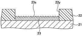
계속해서, 배선 기판(100)의 제조 방법에 관하여 설명한다. 도 2 내지 도 5는, 도 1에 도시된 반도체 장치의 제조 공정을 예시한다. 도 2 내지 도 5에 있어서, 동일 부품에 대해서는, 동일한 부호를 부여하고, 그 설명을 생략한다. 도 2를 참조하면, 구리박으로 이루어지는 지지체(210)를 준비한다. 지지체(210)의 한 쪽의 표면에, 제 1 배선층(110)의 형성 위치에 대응하는 개구부(220x)를 갖는 레지스트층(220)을 형성한다.Next, a method of manufacturing the
도 3을 참조하면, 지지체(210)를 급전층으로 이용하는 전해 도금법에 의해, 지지체(210)의 한 쪽의 표면에 금속층(230) 및 제 1 배선층(110)을 적층한다. 금속층(230)의 재료로서는, 니켈(Ni)을 이용할 수 있다. 제 1 배선층(110)의 재료는 구리(Cu) 등일 수 있다. 제 1 배선층(110)의 면(110s)은 금속층(230)의 면(230s)과 접촉하고 있다.Referring to FIG. 3, a
도 4를 참조하면, 도 3에 나타낸 레지스트층(220)을 제거한 후, 지지체(210)의 한 쪽의 표면에 금속층(230) 및 제 1 배선층(110)을 덮도록 제 1 절연층(120)을 형성한다. 제 1 절연층(120)에 제 1 비아 홀(120x)을 형성하고 나서, 제 1 절연층(120) 상에, 제 1 비아 홀(120x)을 통해 제 1 배선층(110)과 전기적으로 접속되는 제 2 배선층(130)을 형성한다. 제 1 절연층(120) 상에 제 2 배선층(130)을 덮도록 제 2 절연층(140)을 형성하고, 필요할 경우, 다른 배선층 및 절연층을 적층한다.Referring to FIG. 4, after removing the
도 5에 나타낸 공정에서는, 도 4에 나타낸 지지체(210)를 제거한다. 구리박으로 이루어지는 지지체(210)를 제거하며, 금속층(230)을 제거하지 않는 에칭액이 이용된다. 이에 따라, 금속층(230)은 에칭 스톱층으로 기능하여, 지지체(210)만을 제거할 수 있다.In the step shown in Fig. 5, the
다음으로, 니켈(Ni)로 이루어지는 금속층(230)만을 제거할 수 있는 에칭액을 이용하여, 금속층(230)을 에칭에 의해 제거한다. 이에 따라, 제 1 배선층(110)의 면(110s)은 외부에 노출되고, 도 1에 나타낸 배선 기판(100)이 완성된다.Next, the
그런데, 전해 도금법에 의해 형성된, 니켈(Ni)로 이루어지는 금속층(230)의 면(230s)은 평활면이다. 그 때문에, 도 5에 나타낸 공정 후에 노출된, 금속층(230)의 면(230s)과 접촉하고 있었던 제 1 배선층(110)의 면(110s)(전극 패드(110a)의 면(110s) 및 위치 맞춤 마크(110b)의 면(110s))도 평활면으로 된다. 평활면의 표면 거칠기(Ra)는 50㎚ 이하이다(Ra≤50㎚).Incidentally, the
전술한 바와 같이, 위치 맞춤 마크(110b)는, 반도체 칩 등의 전자 부품과 배선 기판(100)의 위치 맞춤의 기준이나, 배선 기판(100)과 다른 배선 기판의 위치 맞춤의 기준 등으로서 이용된다. 위치 맞춤 마크(110b)의 면(110s)이 평활면이면, 반도체 칩과 배선 기판(100)이 적절하게 위치 맞춤되지 않는다는 문제가 생긴다. 이 문제를, 도 6을 참조하여 설명한다.As described above, the
도 6은, 예로서의 위치 맞춤 마크가 광을 반사하는 상태를 도시한다. 도 6에 있어서, 동일 부품에 대해서는, 동일한 부호를 부여하고, 그 설명을 생략한다. 또한, 도 6은 배선 기판(100)이 반전되어 도시되어 있다. 전극 패드(110a)는, 반도체 칩과 접속되는 접속 단자로서 이용된다. 즉, 반도체 칩이 배선 기판(100)의 전극 패드(110a)측에 설치되는 동안, 반도체 칩과 배선 기판(100)의 위치 맞춤이 필요하게 된다.Fig. 6 shows a state in which an alignment mark as an example reflects light. In FIG. 6, the same components are denoted by the same reference numerals, and a description thereof will be omitted. 6, the
도 6을 참조하면, 반도체 칩(도시 생략)과 배선 기판(100)의 위치 맞춤 등의 시에는, 광원(910)에 의해 위치 맞춤 마크(110b)의 면(110s)에 가시광 등을 조사한다. 면(110s)에서의 반사광을 CCD 카메라 등의 수광부(920)에 의해 수광함으로써, 위치 맞춤 마크(110b)를 인식한다. 인식된 위치 맞춤 마크(110b)를 기준으로 해서, 반도체 칩(도시 생략)과 배선 기판(100)의 위치 맞춤을 행한다. 또한, 광원(910)은 수광부(920)를 가로막지 않는 위치에 배치될 필요가 있기 때문에, 조사 광은 위치 맞춤 마크(110b)의 면(110s)에 비스듬히 입사될 수 있다.6, visible light or the like is irradiated to the
여기에서, 위치 맞춤 마크(110b)의 면(110s)이 평활면이면, 광원(910)으로부터의 조사 광은 면(110s)에 있어서는 거의 난반사되지 않는다. 그 때문에 광원(910)으로부터의 조사 광의 대부분은, 입사각(조사 광과 Z축 사이의 각)과 대략 동일한 반사각(반사광과 Z축 사이의 각)을 갖는 반사광으로 된다. 그러므로, 반사광은 수광부(920)를 향해 진행되지 않고, 도 6에 나타낸 화살표 방향으로 진행된다. 그 결과, 광원(910)으로부터의 조사 광의 대부분은 수광부(920)에는 입사되지 않는다. 따라서, 위치 맞춤 마크(110b)를 인식하는 것이 곤란하다. 위치 맞춤 마크(110b)를 인식할 수 없으면, 반도체 칩을 배선 기판(100)에 설치할 수 없는 문제가 생긴다.Here, if the
따라서, 상기 논의된 하나 이상의 문제점을 해결하기 위해서, 본 발명의 실시형태는, 신규하고 유용한, 용이하게 인식하는 것이 가능한 위치 맞춤 마크를 갖는 배선 기판, 그 배선 기판의 제조 방법, 및 상기 배선 기판에 반도체 칩 및 칩 커패시터 등의 각종 전자 부품을 설치한 반도체 패키지를 제공하는 것을 과제로 한다.Accordingly, in order to solve one or more of the problems discussed above, embodiments of the present invention provide a wiring board having an alignment mark that is new and useful, which can be easily recognized, a method of manufacturing the wiring board, And a semiconductor package provided with various electronic parts such as semiconductor chips and chip capacitors.
더 구체적으로는, 본 발명의 실시형태는 절연층, 상기 절연층의 표면에 형성된 오목부, 및 상기 오목부 내에 형성된 위치 맞춤 마크를 포함하고, 상기 위치 맞춤 마크의 한 쪽의 면은, 조화면으로 되는 동시에 상기 절연층의 표면으로부터 오목해지며, 상기 오목부로부터 노출되는 배선 기판을 제공할 수 있다.More specifically, an embodiment of the present invention includes an insulating layer, a concave portion formed on a surface of the insulating layer, and an alignment mark formed in the concave portion, And at the same time, the wiring board which is recessed from the surface of the insulating layer and is exposed from the concave portion can be provided.
본 발명의 다른 양태는, 지지체의 한 쪽의 표면에 금속층을 형성하는 공정, 상기 금속층에 위치 맞춤 마크로 되는 배선층을 적층하는 공정, 상기 금속층 및 상기 배선층을 덮도록, 상기 지지체의 상기 한 쪽의 표면에 절연층을 형성하는 공정, 상기 배선층의 한 쪽의 면을 조화면으로 하는 공정, 및 상기 지지체 및 상기 금속층을 제거함으로써, 상기 절연층으로부터 상기 배선층의 한 쪽의 면을 노출하는 공정을 포함하는 배선 기판의 제조 방법을 제공할 수 있다.According to another aspect of the present invention, there is provided a method of manufacturing a semiconductor device, comprising the steps of: forming a metal layer on one surface of a support; laminating a wiring layer to be a alignment mark on the metal layer; Exposing one surface of the wiring layer from the insulating layer by removing the support and the metal layer; and a step of exposing one surface of the wiring layer from the insulating layer by removing the support and the metal layer A method of manufacturing a wiring board can be provided.
본 발명의 다른 양태는, 반도체 칩, 및 상기 반도체 칩이 탑재되는 배선 기판을 포함하고, 상기 배선 기판은 절연층, 상기 절연층의 표면에 형성된 오목부, 및 상기 오목부 내에 형성된 위치 맞춤 마크를 포함하고, 상기 위치 맞춤 마크의 한 쪽의 면은, 조화면으로 되는 동시에 상기 절연층의 표면으로부터 오목해지며, 상기 오목부로부터 노출되는 반도체 패키지를 제공할 수 있다.According to another aspect of the present invention, there is provided a semiconductor device comprising: a semiconductor chip; and a wiring board on which the semiconductor chip is mounted, wherein the wiring board has an insulating layer, a concave portion formed on a surface of the insulating layer, And one surface of the alignment mark is provided with a roughened surface and concave from the surface of the insulating layer and exposed from the concave portion.
개시의 기술에 의하면, 용이하게 인식하는 것이 가능한 위치 맞춤 마크를 갖는 배선 기판, 그 제조 방법, 및 상기 배선 기판에 반도체 칩이나 칩 커패시터 등의 각종 전자 부품을 탑재한 반도체 패키지를 제공할 수 있다.According to the disclosure, it is possible to provide a wiring board having an alignment mark that can be easily recognized, a manufacturing method thereof, and a semiconductor package having various electronic components such as a semiconductor chip and a chip capacitor mounted on the wiring board.
도 1은 종래의 배선 기판을 예시하는 단면도.
도 2는 종래의 배선 기판의 제 1 제조 공정을 예시하는 도면.
도 3은 종래의 배선 기판의 제 2 제조 공정을 예시하는 도면.
도 4는 종래의 배선 기판의 제 3 제조 공정을 예시하는 도면.
도 5는 종래의 배선 기판의 제 4 제조 공정을 예시하는 도면.
도 6은 종래의 위치 맞춤 마크가 광을 반사하는 상태를 설명하기 위한 도면.
도 7은 제 1 실시형태에 따른 배선 기판을 예시하는 단면도.
도 8은 제 1 실시형태에 따른 배선 기판의 제 1 제조 공정을 예시하는 단면도.
도 9는 제 1 실시형태에 따른 배선 기판의 제 2 제조 공정을 예시하는 단면도.
도 10은 제 1 실시형태에 따른 배선 기판의 제 3 제조 공정을 예시하는 단면도.
도 11은 제 1 실시형태에 따른 배선 기판의 제 4 제조 공정을 예시하는 단면도.
도 12는 제 1 실시형태에 따른 배선 기판의 제 5 제조 공정을 예시하는 단면도.
도 13은 제 1 실시형태에 따른 배선 기판의 제 6 제조 공정을 예시하는 단면도.
도 14는 제 1 실시형태에 따른 배선 기판의 제 7 제조 공정을 예시하는 단면도.
도 15는 제 1 실시형태에 따른 배선 기판의 제 8 제조 공정을 예시하는 단면도.
도 16은 제 1 실시형태에 따른 배선 기판의 제 9 제조 공정을 예시하는 단면도.
도 17은 제 1 실시형태에 따른 배선 기판의 제 10 제조 공정을 예시하는 단면도.
도 18은 제 1 실시형태에 따른 배선 기판의 제 11 제조 공정을 예시하는 단면도.
도 19는 제 1 실시형태에 따른 배선 기판의 제 12 제조 공정을 예시하는 단면도.
도 20은 제 1 실시형태에 따른 배선 기판의 제 13 제조 공정을 예시하는 단면도.
도 21은 제 1 실시형태에 따른 위치 맞춤 마크가 광을 반사하는 상태를 설명하기 위한 도면.
도 22는 제 2 실시형태에 따른 배선 기판의 제 1 제조 공정을 예시하는 단면도.
도 23은 제 2 실시형태에 따른 배선 기판의 제 2 제조 공정을 예시하는 단면도.
도 24는 제 2 실시형태에 따른 배선 기판의 제 3 제조 공정을 예시하는 단면도.
도 25는 제 2 실시형태에 따른 배선 기판의 제 4 제조 공정을 예시하는 단면도.
도 26은 제 3 실시형태에 따른 배선 기판의 제 5 제조 공정을 예시하는 단면도.
도 27은 제 4 실시형태에 따른 배선 기판을 예시하는 단면도.
도 28은 제 4 실시형태에 따른 배선 기판의 제 1 제조 공정을 예시하는 단면도.
도 29는 제 4 실시형태에 따른 배선 기판의 제 2 제조 공정을 예시하는 단면도.
도 30은 제 4 실시형태에 따른 배선 기판의 제 3 제조 공정을 예시하는 단면도.
도 31은 제 4 실시형태에 따른 배선 기판의 제 4 제조 공정을 예시하는 단면도.
도 32는 제 5 실시형태에 따른 반도체 패키지를 예시하는 단면도.
도 33은 제 5 실시형태에 따른 반도체 패키지의 제 1 제조 공정을 예시하는 단면도.
도 34는 제 5 실시형태에 따른 반도체 패키지의 제 2 제조 공정을 예시하는 단면도.
도 35는 제 5 실시형태의 변형예에 따른 반도체 패키지를 예시하는 단면도.1 is a cross-sectional view illustrating a conventional wiring board;
2 is a diagram illustrating a first manufacturing process of a conventional wiring board;
3 is a diagram illustrating a second manufacturing process of a conventional wiring board;
4 is a diagram illustrating a third manufacturing process of a conventional wiring board;
5 is a diagram illustrating a fourth manufacturing process of a conventional wiring board;
6 is a view for explaining a state in which a conventional alignment mark reflects light.
7 is a cross-sectional view illustrating a wiring board according to the first embodiment;
8 is a cross-sectional view illustrating a first manufacturing process of a wiring board according to the first embodiment;
9 is a cross-sectional view illustrating a second manufacturing process of the wiring board according to the first embodiment;
10 is a cross-sectional view illustrating a third manufacturing process of the wiring board according to the first embodiment;
11 is a cross-sectional view illustrating a fourth manufacturing process of the wiring board according to the first embodiment;
12 is a cross-sectional view illustrating a fifth manufacturing process of the wiring board according to the first embodiment;
13 is a cross-sectional view illustrating a sixth manufacturing process of the wiring board according to the first embodiment;
14 is a cross-sectional view illustrating a seventh manufacturing process of the wiring board according to the first embodiment;
15 is a cross-sectional view illustrating an eighth manufacturing process of the wiring board according to the first embodiment;
16 is a cross-sectional view illustrating a ninth manufacturing process of the wiring board according to the first embodiment;
17 is a cross-sectional view illustrating a tenth manufacturing process of the wiring board according to the first embodiment;
18 is a cross-sectional view illustrating an eleventh manufacturing process of the wiring board according to the first embodiment;
19 is a cross-sectional view illustrating a twelfth manufacturing process of the wiring board according to the first embodiment;
20 is a cross-sectional view illustrating a thirteenth manufacturing process of the wiring board according to the first embodiment;
21 is a view for explaining a state in which an alignment mark according to the first embodiment reflects light.
22 is a cross-sectional view illustrating a first manufacturing process of the wiring board according to the second embodiment;
23 is a cross-sectional view illustrating a second manufacturing process of the wiring board according to the second embodiment;
24 is a cross-sectional view illustrating a third manufacturing process of the wiring board according to the second embodiment;
25 is a cross-sectional view illustrating a fourth manufacturing process of the wiring board according to the second embodiment;
26 is a cross-sectional view illustrating a fifth manufacturing process of the wiring board according to the third embodiment;
27 is a cross-sectional view illustrating a wiring board according to a fourth embodiment;
28 is a cross-sectional view illustrating a first manufacturing process of a wiring board according to a fourth embodiment;
29 is a cross-sectional view illustrating a second manufacturing process of the wiring board according to the fourth embodiment;
30 is a cross-sectional view illustrating a third manufacturing process of the wiring board according to the fourth embodiment;
31 is a cross-sectional view illustrating a fourth manufacturing process of the wiring board according to the fourth embodiment;
32 is a cross-sectional view illustrating a semiconductor package according to a fifth embodiment;
33 is a cross-sectional view illustrating a first manufacturing process of the semiconductor package according to the fifth embodiment;
34 is a cross-sectional view illustrating a second manufacturing process of the semiconductor package according to the fifth embodiment;
35 is a cross-sectional view illustrating a semiconductor package according to a modification of the fifth embodiment;
상기 실시형태의 추가적인 목적 및 이점은 다음의 설명에서 부분적으로 기술되며, 그 설명으로부터 부분적으로 명확해지거나, 또는 본 발명의 실시에 의해 이해될 것이다. 본 발명의 목적 및 이점은 특허청구범위에 특별히 지시된 구성 요소 및 조합에 의해 실현되어 달성할 수 있다. 전술한 일반적인 설명 및 다음의 상세한 설명의 모두는 예시 및 설명적인 것으로, 본 발명을 청구된 바와 같이 제한하는 것이 아님을 이해해야 한다.Additional objects and advantages of the embodiments will be set forth in part in the description that follows, and in part will be obvious from the description, or may be learned by practice of the invention. The objects and advantages of the invention may be realized and attained by means of the elements and combinations particularly pointed out in the claims. It is to be understood that both the foregoing general description and the following detailed description are exemplary and explanatory and are not restrictive of the invention as claimed.
제 1 실시형태First Embodiment
[제 1 실시형태에 따른 배선 기판의 구조][Structure of the wiring board according to the first embodiment]
먼저, 제 1 실시형태에 따른 배선 기판의 구조에 관하여 설명한다. 도 7은, 제 1 실시형태에 따른 배선 기판을 예시하는 단면도이다. 도 7을 참조하면, 배선 기판(10)은, 제 1 배선층(11), 제 1 절연층(12), 제 2 배선층(13), 제 2 절연층(14), 제 3 배선층(15), 제 3 절연층(16), 제 4 배선층(17), 및 솔더레지스트층(18)이 적층된 구조를 갖는다.First, the structure of the wiring board according to the first embodiment will be described. 7 is a cross-sectional view illustrating a wiring board according to the first embodiment. 7, the
배선 기판(10)에 있어서, 제 1 배선층(11)은, 제 1 절연층(12)의 표면(12a)에 형성된 오목부(12y) 내에 설치되어 있다. 제 1 배선층(11)의 면(11s)은 제 1 절연층(12)의 표면(12a) 상의 오목부로부터 노출되어 있다. 제 1 절연층(12)의 표면(12a)으로부터 제 1 배선층(11)의 면(11s)까지의 깊이 또는 거리는 약 5㎛ 내지 15㎛일 수 있다. 제 1 배선층(11)의 재료는 구리(Cu) 등일 수 있다. 제 1 배선층(11)의 두께는 약 15㎛ 내지 20㎛일 수 있다. 오목부(12y)는 평면에서 볼 때 원형으로 형성될 수 있다. 제 1 절연층(12)의 재료는 에폭시 수지나 폴리이미드 수지 등의 절연 수지일 수 있다. 제 1 절연층(12)의 두께는 50㎛일 수 있다.In the
제 1 배선층(11)은, 전극 패드(11a)와 위치 맞춤 마크(11b)를 포함한다. 전극 패드(11a)는, 반도체 칩, 칩 커패시터, 칩 레지스터, 및 칩 인덕터 등의 각종 전자 부품과 접속되는 접속 단자이다. 전극 패드(11a)는 평면에서 볼 때 원형으로 형성될 수 있고, 그 직경은 약 50㎛일 수 있다.The
위치 맞춤 마크(11b)는, 반도체 칩 등의 전자 부품과 배선 기판(10)의 위치 맞춤의 기준이나, 배선 기판(10)과 다른 배선 기판의 위치 맞춤의 기준 등으로서 이용된다. 위치 맞춤 마크(11b)는, 예를 들면 평면에서 볼 때 원형으로 형성될 수 있고, 그 직경은 약 0.3㎜일 수 있다. 다만, 위치 맞춤 마크(11b)는, 평면에서 볼 때 원형으로 형성될 필요는 없고, 평면에서 볼 때 직사각형이나 십자형 등의 임의의 형상으로 해도 상관없다.The
제 1 배선층(11)의 면(11s)(전극 패드(11a)의 면(11s) 및 위치 맞춤 마크(11b)의 면(11s))은, 소정의 표면 거칠기의 조화면으로 되어 있다. 이하에서, 조화면은 50㎚보다 큰 표면 거칠기 Ra를 가진다(Ra>50㎚). 제 1 배선층(11)의 면(11s)(전극 패드(11a)의 면(11s) 및 위치 맞춤 마크(11b)의 면(11s))의 소정의 표면 거칠기(Ra)는 약 150㎚인 것이 바람직하다. 그러나, 50㎚<Ra<200㎚이면, 본 발명에 포함된다. 제 1 배선층(11)의 조화면(11s)의 표면 거칠기(Ra)를 50㎚<Ra<200㎚로 하는 기술적인 의의에 관해서는 후술한다.The
제 2 배선층(13)은, 제 1 절연층(12)의 표면(12b)측에 형성되어 있다. 제 2 배선층(13)은, 제 1 절연층(12)을 관통하고, 제 1 비아 홀(12x) 내에 충전되며, 그 상면이 노출되는 비아, 및 제 1 절연층(12)의 표면(12b)에 형성된 배선 패턴을 포함한다. 제 2 배선층(13)은, 제 1 비아 홀(12x)을 향해 노출된 전극 패드(11a)와 전기적으로 접속되어 있다. 제 2 배선층(13)의 재료는 구리(Cu) 등일 수 있다. 제 2 배선층(13)의 두께는 약 15㎛ 내지 20㎛일 수 있다.The
제 2 절연층(14)은, 제 1 절연층(12) 상의 제 2 배선층(13)을 덮도록 형성되어 있다. 제 2 절연층(14)의 재료로서는, 에폭시 수지나 폴리이미드 수지일 수 있다. 제 2 절연층(14)의 두께는 약 50㎛일 수 있다.The second insulating
제 3 배선층(15)은 제 2 절연층(14) 상에 형성되어 있다. 제 3 배선층(15)은, 제 2 절연층(14)을 관통하고, 제 2 비아 홀(14x) 내에 충전되며, 그 상면이 노출되는 비아, 및 제 2 절연층(14) 표면에 형성된 배선 패턴을 포함한다. 제 3 배선층(15)은, 제 2 비아 홀(14x)을 향해 노출된 제 2 배선층(13)과 전기적으로 접속되어 있다. 제 3 배선층(15)의 재료는 구리(Cu) 등일 수 있다. 제 3 배선층(15)의 두께는 약 15㎛ 내지 20㎛일 수 있다.The
제 3 절연층(16)은, 제 2 절연층(14) 상에, 제 3 배선층(15)을 덮도록 형성되어 있다. 제 3 절연층(16)의 재료는 에폭시 수지나 폴리이미드 수지일 수 있다. 제 3 절연층(16)의 두께는 약 50㎛일 수 있다.The third insulating
제 4 배선층(17)은 제 3 절연층(16) 상에 형성되어 있다. 제 4 배선층(17)은, 제 3 절연층(16)을 관통하고, 제 3 비아 홀(16x) 내에 충전되며, 그 상면이 노출되는 비아, 및 제 3 절연층(16) 상에 형성된 배선 패턴을 포함한다. 제 4 배선층(17)은, 제 3 비아 홀(16x)을 향해 노출된 제 3 배선층(15)과 전기적으로 접속되어 있다. 제 4 배선층(17)의 재료는 구리(Cu) 등일 수 있다. 제 4 배선층(17)의 두께는 약 15㎛ 내지 20㎛일 수 있다.The
솔더레지스트층(18)은, 제 3 절연층(16) 상에, 제 4 배선층(17)을 덮도록 형성되어 있다. 솔더레지스트층(18)은 개구부(18x)를 갖고, 제 4 배선층(17)의 일부는 솔더레지스트층(18)의 개구부(18x)의 내부를 향해 노출되어 있다. 솔더레지스트층(18)의 재료는 에폭시 수지나 이미드 수지 등을 포함하는 감광성 수지 조성물일 수 있다. 솔더레지스트층(18)의 두께는 약 50㎛일 수 있다.The solder resist
필요할 경우, 개구부(18x) 내부를 향해 노출되는 제 4 배선층(17) 상에, 금속층 등을 형성해도 된다. 금속층의 예는, Au층이나, Ni/Au층(Ni층과 Au층을 이 순서로 적층한 금속층), Ni/Pd/Au층(Ni층과 Pd층과 Au층을 이 순서로 적층한 금속층)이다.If necessary, a metal layer or the like may be formed on the
또한, 솔더레지스트층(18)의 개구부(18x) 내부를 향해 노출되는 제 4 배선층(17) 상에(제 4 배선층(17) 상에 금속층 등이 형성되어 있을 경우에는, 금속층 등의 상에) 솔더 볼이나 리드 핀 등의 외부 접속 단자를 형성해도 상관없다. 외부 접속 단자는, 마더보드 등의 실장 기판(도시 생략)에 설치된 패드와 전기적으로 접속하기 위한 단자이며, 필요할 경우 형성될 수 있다.In addition, on the
[제 1 실시형태에 따른 배선 기판의 제조 방법][Method of manufacturing wiring board according to the first embodiment]
계속해서, 제 1 실시형태에 따른 배선 기판의 제조 방법에 관하여 설명한다. 도 8 내지 도 20은, 제 1 실시형태에 따른 배선 기판의 제조 공정을 예시하는 도면이다. 도 8 내지 도 20에 있어서, 도 7과 동일 부품에 대해서는, 동일한 부호를 부여하고, 그 설명을 생략한다.Next, a method for manufacturing a wiring board according to the first embodiment will be described. Figs. 8 to 20 are views showing the steps of manufacturing the wiring board according to the first embodiment. Fig. In Figs. 8 to 20, the same components as those in Fig. 7 are denoted by the same reference numerals, and a description thereof will be omitted.
도 8을 참조하면, 지지체(21)를 준비한다. 지지체(21)로서는, 실리콘판, 글래스판, 금속판, 금속박 등이다. 본 실시형태에서는, 지지체(21)로서 구리박을 이용한다. 이는 도 10에 나타낸 공정에 있어서 지지체가 전해 도금용 급전층으로서 이용되기 때문이다. 도 17에 나타낸 공정에 있어서 지지체는 용이하게 제거 가능하다. 지지체(21)의 두께는 약 35㎛ 내지 100㎛일 수 있다.Referring to Fig. 8, a
도 9를 참조하면, 제 1 배선층(11)을 구성하는 전극 패드(11a)의 형성 위치에 대응하는 개구부(22x), 및 제 1 배선층(11)을 구성하는 위치 맞춤 마크(11b)의 형성 위치에 대응하는 개구부(22y)를 갖는 레지스트층(22)을 형성한다. 레지스트층(22)의 두께는 약 30㎛ 내지 50㎛일 수 있다.9, the
구체적으로는, 지지체(21)의 한 쪽의 표면에, 에폭시 수지나 이미드 수지 등을 포함하는 감광성 수지 조성물로 이루어지는 액상 또는 페이스트 레지스트를 도포한다. 또는, 지지체(21)의 한 쪽의 표면에, 에폭시 수지나 이미드 수지 등을 포함하는 감광성 수지 조성물로 이루어지는 드라이 필름 레지스트 등의 필름 레지스트를 적층한다. 레지스트층(22)을 노광하고 도포 또는 적층된 레지스트를 현상함으로써, 개구부(22x 및 22y)를 형성한다. 이에 따라, 개구부(22x 및 22y)를 갖는 레지스트층(22)이 형성된다. 개구부(22x 및 22y)를 가지는 필름 레지스트를 지지체(21)의 한 쪽의 표면에 적층해도 상관없다.Specifically, a liquid or paste resist made of a photosensitive resin composition containing an epoxy resin, an imide resin, or the like is applied to one surface of the
개구부(22x)는 제 1 배선층(11)을 구성하는 전극 패드(11a)에 대응하는 위치에 형성된다. 전극 패드의 배치 피치는 약 100㎛일 수 있다. 개구부(22x)는 평면에서 볼 때 원형으로 형성될 수 있고, 그 직경은 약 50㎛일 수 있다. 개구부(22y)는 평면에서 볼 때 원형으로 형성될 수 있고, 그 직경은 0.3㎜일 수 있다. 위치 맞춤 마크(11b)는, 평면에서 볼 때 원형으로 형성될 필요는 없고, 평면에서 볼 때 직사각형 및 십자형 등의 임의의 형상으로 해도 상관없다.The
도 10을 참조하면, 지지체(21)를 급전층으로 이용하는 전해 도금법에 의해, 개구부(22x 및 22y) 내의 지지체(21)의 한 쪽의 표면에 금속층(23)을 형성한다. 금속층(23)은, 후술하는 도 17에 나타낸 공정에서 지지체(21)를 제거할 때에, 제 1 배선층(11)이 제거되는 것을 방지하기 위해 설치된다. 금속층(23)은 에칭 스톱층으로서 기능한다. 금속층(23)의 재료는 지지체(21)를 제거하기 위한 에칭액에 의해 제거되지 않는다.10, a
구체적으로는, 제 1 실시형태에서는 지지체(21)로서 구리박을 이용하고 있기 때문에, 금속층(23)의 재료는, 구리(Cu)를 제거하기 위한 에칭액에 의해 제거할 수 없는 니켈(Ni)을 이용한다. 니켈(Ni)로 구성되는 금속층(23)은, 예를 들면 도금욕(plating bath)으로서 술폰산 니켈욕에서 전해 도금법에 의해 형성될 수 있다. 도금욕으로서 술폰산 니켈욕에서 전해 도금법에 의해 형성된 니켈(Ni)로 구성되는 금속층(23)의 표면(23s)은 평활면으로 된다. 여기에서, 평활면은 50㎚ 이하의 표면 거칠기를 가진다(Ra≤50㎚). 그러나, 금속층(23)은, 구리(Cu)를 제거하기 위한 에칭액에 의해 제거할 수 없는 것이면, 니켈(Ni) 이외의 재료를 이용해도 상관없다. 금속층(23)의 두께는 약 5㎛ 내지 15㎛일 수 있다.Specifically, since the copper foil is used as the
도 11을 참조하면, 지지체(21)를 급전층으로 이용하는 전해 도금법에 의해, 개구부(22x 및 22y) 내의 금속층(23)의 면(23s)에 제 1 배선층(11)을 형성한다. 제 1 배선층(11)의 재료는 구리(Cu) 등일 수 있다. 제 1 배선층(11)의 두께는 약 15㎛ 내지 20㎛이다. 제 1 배선층(11)은, 전극 패드(11a)와 위치 맞춤 마크(11b)를 포함한다. 전극 패드(11a)는, 반도체 칩과 접속되는 접속 단자로서 이용된다. 위치 맞춤 마크(11b)는, 반도체 칩 등의 전자 부품과 배선 기판(10)의 위치 맞춤의 기준이나, 배선 기판(10)과 다른 배선 기판의 위치 맞춤의 기준으로서 이용된다. 이렇게, 전극 패드(11a)와 위치 맞춤 마크(11b)는, 동일 공정에 있어서 형성된다.11, the
다음으로, 도 12를 참조하면, 도 11에 나타낸 레지스트층(22)을 제거한 후, 금속층(23) 및 제 1 배선층(11)을 덮도록 지지체(21)의 한 쪽의 표면에 제 1 절연층(12)을 형성한다. 제 1 절연층(12)의 재료는 열경화성 필름 형상의 에폭시 수지나 폴리이미드 수지 등, 또는 열경화성 액상 또는 페이스트 형상의 에폭시 수지나 폴리이미드 수지일 수 있다. 제 1 절연층(12)은, 후술하는 공정에서 레이저 가공법 등에 의해 제 1 비아 홀(12x)을 형성하기 쉽게 할 수 있도록, 필러가 함유된 가공성이 우수한 수지재를 이용하는 것이 바람직하다. 제 1 절연층(12)의 두께는 약 50㎛이다.12, after the resist
제 1 절연층(12)의 재료로서 필름 형상의 에폭시 수지나 폴리이미드 수지, 열경화성 액상 또는 페이스트 형상의 에폭시 수지나 폴리이미드 수지 등을 이용했을 경우에는, 금속층(23) 및 제 1 배선층(11)을 덮도록 지지체(21)의 표면에 필름 형상의 제 1 절연층(12)을 적층할 수 있다. 적층된 제 1 절연층(12)을 가압한 후, 제 1 절연층(12)을 경화 온도 이상으로 가열해서 경화시킨다. 제 1 절연층(12)을 진공 분위기 하에서 적층함으로써, 보이드가 형성되는 것을 방지할 수 있다.A
제 1 절연층(12)의 재료로서 열경화성 액상 또는 페이스트 형상의 에폭시 수지나 폴리이미드 수지 등을 이용했을 경우에는, 금속층(23) 및 제 1 배선층(11)을 덮도록 액상 또는 페이스트 형상의 제 1 절연층(12)을, 예를 들면 스핀 코팅법 등에 의해 도포할 수 있다. 그리고, 도포한 제 1 절연층(12)을 경화 온도 이상으로 가열해서 경화시킨다.When a thermosetting liquid epoxy resin, a polyimide resin, or the like is used as the material of the
도 13을 참조하면, 제 1 절연층(12)에, 제 1 절연층(12)을 관통하고 제 1 배선층(11)의 면을 노출시키는 제 1 비아 홀(12x)을 형성한다. 제 1 비아 홀(12x)은, 예를 들면 CO2 레이저를 이용한 레이저 가공법에 의해 형성될 수 있다. 제 1 비아 홀(12x)은, 제 1 절연층(12)으로서 감광성 수지를 이용하고, 포토리스그래피법에 의해 제 1 절연층(12)을 패터닝함으로써 형성할 수 있다. 또한, 제 1 비아 홀(12x)은, 제 1 비아 홀(12x)에 대응하는 위치를 마스크하는 스크린 마스크를 통해 액상 또는 페이스트 형상의 수지를 인쇄하고 경화시킴으로써 형성해도 상관없다.13, a first via
도 14를 참조하면, 제 1 절연층(12)의 표면(12b)측에 제 2 배선층(13)을 형성한다. 제 2 배선층(13)은, 제 1 비아 홀(12x) 내에 충전된 비아, 및 제 1 절연층(12)의 표면(12b)에 형성된 배선 패턴을 포함해서 구성된다. 제 2 배선층(13)은, 제 1 비아 홀(12x)을 향해 노출된 제 1 배선층(11)의 전극 패드(11a)와 전기적으로 접속된다. 제 2 배선층(13)의 재료는 구리(Cu) 등일 수 있다.Referring to FIG. 14, a
제 2 배선층(13)은, 세미애디티브법(semi-additive method)이나 서브트랙티브법(subtractive method)의 각종의 배선 형성 방법을 이용하여 형성할 수 있다. 예로서, 세미애디티브법을 이용하여 제 2 배선층(13)을 형성하는 방법을 이하에 나타낸다.The
먼저, 무전해 도금법 또는 스퍼터링법에 의해, 제 1 비아 홀(12x) 내에 노출된 제 1 배선층(11)의 전극 패드(11a)의 상면, 및 제 1 비아 홀(12x)의 내벽을 포함하는 제 1 절연층(12) 상에 구리(Cu) 등으로 이루어지는 시드층(도시 생략)을 형성한다. 또한, 시드층 상에 제 2 배선층(13)에 대응하는 개구부를 구비한 레지스트층(도시 생략)을 형성한다. 시드층을 급전층으로서 이용한 전해 도금법에 의해, 레지스트층의 개구부에 구리(Cu)로 이루어지는 배선층(도시 생략)을 형성한다. 계속해서, 레지스트층을 제거한 후에, 배선층을 마스크로 이용해서, 배선층으로 덮여 있지 않은 부분의 시드층을 에칭에 의해 제거한다. 이에 따라, 제 1 절연층(12) 상에, 제 1 비아 홀(12x) 내에 충전된 비아 및 제 1 절연층(12) 상에 형성된 배선 패턴을 포함해서 구성되는 제 2 배선층(13)이 형성된다.First, the upper surface of the
도 15를 참조하면, 상기와 동일한 공정을 반복함으로써, 제 2 절연층(14), 제 3 배선층(15), 제 3 절연층(16), 및 제 4 배선층(17)을 적층한다. 즉, 제 1 절연층(12)의 표면(12b)에 제 2 배선층(13)을 피복하는 제 2 절연층(14)을 형성한 후에, 제 2 배선층(13) 상의 제 2 절연층(14)의 부분에 제 2 비아 홀(14x)을 형성한다. 제 2 절연층(14)의 재료는, 열경화성 필름 형상의 에폭시 수지나 폴리이미드 수지, 또는 열경화성 액상 또는 페이스트 형상의 에폭시 수지나 폴리이미드 수지일 수 있다.Referring to FIG. 15, the second insulating
또한, 제 2 절연층(14) 상에, 제 2 비아 홀(14x)을 통해 제 2 배선층(13)에 접속되는 제 3 배선층(15)을 형성한다. 제 3 배선층(15)의 재료는 구리(Cu) 등이다. 제 3 배선층(15)은 세미애디티브법에 의해 형성될 수 있다.A
제 2 절연층(14) 상에 제 3 배선층(15)을 피복하는 제 3 절연층(16)을 형성한 후에, 제 3 배선층(15) 상의 제 3 절연층(16)의 부분에 제 3 비아 홀(16x)을 형성한다. 또한, 제 3 절연층(16) 상에, 제 3 비아 홀(16x)을 통해 제 3 배선층(15)에 접속되는 제 4 배선층(17)을 형성한다. 제 3 절연층(16)의 재료로서는, 예를 들면 열경화성 필름 형상의 에폭시 수지나 폴리이미드 수지, 또는 열경화성 액상 또는 페이스트 형상의 에폭시 수지나 폴리이미드 수지일 수 있다. 제 4 배선층(17)의 재료는 구리(Cu) 등이다. 제 4 배선층(17)은 세미애디티브법에 의해 형성될 수 있다.A third insulating
이렇게 하여, 지지체(21)의 한 쪽의 표면에 소정의 빌드업 배선층이 형성된다. 제 1 실시형태에서는, 제 2 배선층(13), 제 3 배선층(15), 및 제 4 배선층(17)을 포함하는 3층의 빌드업 배선을 형성한다. n층(n은 1 이상의 정수)의 빌드업 배선층을 형성하는 것이 가능하다.Thus, a predetermined build-up wiring layer is formed on one surface of the
도 16을 참조하면, 제 3 절연층(16) 상에, 제 4 배선층(17)을 덮도록 개구부(18x)를 갖는 솔더레지스트층(18)을 형성한다. 구체적으로는, 제 3 절연층(16) 상에, 제 4 배선층(17)을 덮도록, 에폭시 수지나 이미드계 수지 등을 포함하는 감광성 수지 조성물로 이루어지는 솔더레지스트를 도포한다. 도포된 솔더레지스트를 노광 및 현상함으로써, 개구부(18x)를 형성한다. 이에 따라, 개구부(18x)를 갖는 솔더레지스트층(18)이 형성된다. 제 4 배선층(17)의 일부는, 솔더레지스트층(18)의 개구부(18x) 내에 노출된다. 개구부(18x) 내에 노출되는 제 4 배선층(17)은, 마더보드 등의 실장 기판(도시 생략)에 설치된 패드와 전기적으로 접속하기 위해서 전극 패드로서 기능한다.16, a solder resist
필요할 경우, 개구부(18x) 내부를 향해 노출되는 제 4 배선층(17) 상에, 금속층 등을 형성해도 된다. 금속층의 예는, Au층이나, Ni/Au층(Ni층과 Au층을 이 순서로 적층한 금속층), 및 Ni/Pd/Au층(Ni층과 Pd층과 Au층을 이 순서로 적층한 금속층)이다.If necessary, a metal layer or the like may be formed on the
도 17에 나타낸 공정에서는, 도 16에 나타낸 지지체(21)를 제거한다. 구리박으로 구성되어 있는 지지체(21)는, 염화 제2철 수용액이나 염화 제2구리 수용액과 황산 암모늄 수용액 등을 이용한 웨트 에칭에 의해 제거될 수 있다. 이 때, 금속층(23)은 니켈(Ni)로 구성되어 있기 때문에, 에칭 스톱층으로서 기능한다. 따라서, 지지체(21)를 선택적으로 에칭해서 제거할 수 있다. 이 공정에 의해, 금속층(23)의 다른 쪽의 면(면(23s)의 반대면)은, 제 1 절연층(12)으로부터 노출된다. 제 4 배선층(17)이 구리(Cu)로 구성되어 있을 경우에는, 제 4 배선층(17)을 마스크함으로써, 지지체(21)와 함께 에칭되는 것을 방지한다.In the step shown in Fig. 17, the
도 18에 나타낸 공정에서는, 도 17에 나타낸 금속층(23)을 제거한다. 니켈(Ni)로 구성되어 있는 금속층(23)은, 예를 들면 메크(주)(MEC Co., Ltd.) 제조의 니켈 제거액 NH1860 등을 이용한 웨트 에칭에 의해 제거될 수 있다. 이 공정에 의해, 제 1 배선층(11)의 면(11s)은, 제 1 절연층(12)의 표면(12a)에 형성된 오목부(12y) 내의 제 1 절연층(12)의 표면(12a)으로부터 오목해진 위치에서 노출된다. 제 1 절연층(12)의 표면(12a)으로부터 면(11s)까지의 깊이 또는 거리는 약 5㎛ 내지 15㎛일 수 있다. 전술한 바와 같이, 금속층(23)의 면(23s)은 평활면이기 때문에, 금속층(23)의 면(23s)과 접촉하고 있었던 제 1 배선층(11)의 면(11s)(전극 패드(11a)의 면(11s) 및 위치 맞춤 마크(11b)의 면(11s))도 평활면으로 된다.In the step shown in Fig. 18, the
다음으로, 도 19 및 도 20을 참조하면, 제 1 배선층(11)의 면(11s)(전극 패드(11a)의 면(11s) 및 위치 맞춤 마크(11b)의 면(11s))을 소정의 표면 거칠기의 조화면으로 한다. 이에 따라, 도 7에 나타낸 배선 기판(10)이 완성된다. 또한, 도 20은, 도 19의 원 A를 확대해서 예시하는 단면도이다. 제 1 배선층(11)의 면(11s)의 소정의 표면 거칠기는 약 150㎚(Ra=150㎚)인 것이 바람직하다. 그러나, 50㎚<Ra<200㎚의 범위이면 상관없다. 제 1 배선층(11)의 면(11s)은 50㎚<Ra<200㎚의 소정의 표면 거칠기를 가지는 조화면일 수 있다. 제 1 배선층(11)의 면(11s)은 포름산 등의 유기산을 포함하는 약액을 이용한 웨트 에칭이나, 제 1 배선층(11)의 면(11s) 이외의 부분을 마스크한 블라스트 처리 등에 의해 소정의 표면 거칠기가 얻어진다.19 and 20, the
블라스트 처리는 연마제를 피처리물에 고압으로 분사하여, 피처리물의 표면 조도(粗度)를 기계적으로 조정하는 처리이다. 블라스트 처리는, 에어 블라스트 처리, 숏(shot) 블라스트 처리, 웨트 블라스트 처리 등을 포함한다. 알루미나 연마용 입자 및 구 형상 실리카 연마용 입자 등의 연마제를 분산시켜 피처리물에 충돌시켜서, 미세 영역의 연마를 행함으로써 웨트 블라스트 처리가 실시된다. 웨트 블라스트 처리를 이용하면, 에어 블라스트 처리나 숏 블라스트 처리에 비해 매우 치밀하고 손상이 적은 연마가 가능하다. 또한, 연마재를 물 등의 용매에 분산시키기 때문에, 에어 블라스트 처리 및 숏 블라스트 처리와 달리 연마제가 분진으로서 공기 중으로 비산하지 않는다.The blast treatment is a treatment to mechanically adjust the surface roughness of the article to be treated by spraying the article with the abrasive at a high pressure. The blast treatment includes an air blast treatment, a shot blast treatment, a wet blast treatment, and the like. The wet blast treatment is carried out by dispersing the abrasive such as alumina abrasive particles and spherical silica abrasive particles, colliding with the object to be processed, and polishing the fine area. When wet blast treatment is used, it is possible to perform polishing with a very dense and less damage than an air blast treatment or a shot blast treatment. Further, since the abrasive is dispersed in a solvent such as water, unlike the air blast treatment and the shot blast treatment, the abrasive does not scatter into the air as dust.
제 1 배선층(11)의 면(11s)을 조화면으로 하는 기술적인 의의에 관하여 설명한다. 도 21은, 제 1 실시형태에 따른 위치 맞춤 마크가 광을 반사하는 상태를 도시한다. 도 21을 참조하면, 도 7과 동일 부품에 대해서는, 동일한 부호를 부여하고, 그 설명을 생략한다. 또한, 도 21은 배선 기판(10)이 도 7과는 반전되어 도시된 단면도이다. 전극 패드(11a)는, 반도체 칩(도시 생략)과 접속되는 접속 단자로서 이용된다. 반도체 칩은, 배선 기판(10)의 전극 패드(11a)측에 설치되는 동안에, 이 때에 반도체 칩과 배선 기판(10)의 위치 맞춤이 필요하게 된다.The technical significance of making the
도 21을 참조하면, 반도체 칩(도시 생략)과 배선 기판(10)의 위치 맞춤 시에는, 광원(91)에 의해 위치 맞춤 마크(11b)의 면(11s)에 가시광 등을 조사한다. 면(11s)에 있어서의 반사광을 CCD 카메라 등의 수광부(92)에 의해 수광함으로써, 위치 맞춤 마크(11b)를 인식한다. 그리고, 인식된 위치 맞춤 마크(11b)에 의거하여, 반도체 칩과 배선 기판(10)의 위치 맞춤을 행한다. 또한, 광원(91)은 수광부(92)를 가로막지 않는 위치에 배치될 필요가 있기 때문에, 조사 광은 위치 맞춤 마크(11b)의 면(11s)에 비스듬히 입사될 수 있다.21, visible light or the like is irradiated to the
여기에서, 위치 맞춤 마크(11b)의 면(11s)은 조화면이기 때문에, 위치 맞춤 마크(11b)의 면(11s)이 평활면일 경우와는 달리, 광원(91)으로부터의 조사 광은 면(11s)에 있어서 난반사된다. 그 때문에, 광원(91)으로부터의 조사 광의 대부분은 수광부(92)의 방향으로 반사되어 수광부(92)에 입사된다. 따라서, 위치 맞춤 마크(11b)를 용이하게 인식할 수 있다. 위치 맞춤 마크(11b)를 인식할 경우, 반도체 칩을 배선 기판(10)의 올바른 위치에 설치하는 것이 가능해진다.Unlike the case where the
위치 맞춤 마크(11b)의 면(11s)으로의 조사 광을 난반사시킬 경우, 위치 맞춤 마크(11b)의 면(11s)의 표면 거칠기(Ra)는 약 150㎚인 것이 바람직하다. 그러나, 50㎚<Ra<200㎚이면, 허용 가능하다.It is preferable that the surface roughness Ra of the
위치 맞춤 마크(11b)의 면(11s)의 표면 거칠기(Ra)가 50㎚ 이하일 경우(Ra≤50㎚), 즉 위치 맞춤 마크(11b)의 면(11s)이 평활면일 경우에는, 광원(91)으로부터의 조사 광은 면(11s)에 있어서 거의 난반사되지 않는다. 따라서, 광원(91)으로부터의 조사 광의 대부분은 수광부(92)에는 입사되지 않아, 위치 맞춤 마크(11b)를 인식하는 것이 곤란해진다.When the
한편, 위치 맞춤 마크(11b)의 면(11s)의 표면 거칠기(Ra)가 200㎚일 이상일 경우(Ra≥200㎚)에는, 이하의 이유에 의해, 위치 맞춤 마크(11b)를 인식하는 것이 곤란해진다. 광원(91)으로부터의 조사 광은 과잉으로 산란되어, 위치 맞춤 마크(11b)로부터의 반사광은 약해져서, 제 1 절연층(12)의 표면(12a)으로부터의 반사광의 강도와 실질적으로 동일해진다. 그래서, 위치 맞춤 마크(11b)와 면(12a)으로부터의 반사광의 강도 사이의 차이가 작아진다. 상술한 바와 같이, 위치 맞춤 마크(11b)의 면(11s)의 표면 거칠기(Ra)는, 50㎚<Ra<200㎚의 범위이면 바람직하다.On the other hand, when the surface roughness Ra of the
또한, 제 1 절연층(12)의 표면(12a)의 표면 거칠기(Ra)를, 제 1 절연층(12)의 위치 맞춤 마크(11b)의 표면 거칠기(Ra)와 다르게 하는 것이 바람직하다. 이 경우에, 표면(12a) 및 위치 맞춤 마크(11b)의 표면 거칠기의 Ra가 동일할 경우보다, 위치 맞춤 마크(11b)를 더 용이하게 검출할 수 있다. 이 경우, 제 1 절연층(12)의 표면(12a)의 표면 거칠기(Ra)를, 제 1 절연층(12)의 위치 맞춤 마크(11b)의 표면 거칠기보다 크게 하거나 작게 해도, 위치 맞춤 마크(11b)를 검출하기 쉬워진다. 이는 위치 맞춤 마크(11b)로부터의 반사광만이, CCD 카메라 등의 수광부(92)에 입사되기 쉬워지기 때문이다.It is also preferable that the surface roughness Ra of the
제 1 실시형태에 의하면, 반도체 칩과 배선 기판의 위치 맞춤 등에 이용되는 위치 맞춤 마크의 조화면을, 50㎚<Ra<200㎚의 범위의 소정의 표면 거칠기를 가지도록 설정한다. 이에 따라, 반도체 칩과 배선 기판의 위치 맞춤 시에 이용되는 위치 맞춤 마크에 조사되는 광은 위치 맞춤 마크의 조화면에서 난반사되어, 그 대부분이 수광부에 도달한다. 그 결과, 위치 맞춤 시에 위치 맞춤 마크를 용이하게 인식할 수 있기 때문에, 반도체 칩과 배선 기판의 위치 맞춤의 정밀도를 향상할 수 있다.According to the first embodiment, the roughened surface of the alignment mark used for alignment of the semiconductor chip and the wiring board is set to have a predetermined surface roughness in the range of 50 nm <Ra <200 nm. Thus, the light irradiated on the alignment mark used for aligning the semiconductor chip and the wiring substrate is diffusedly reflected on the coarsened surface of the alignment mark, and most of the light reaches the light receiving portion. As a result, since the alignment mark can be easily recognized at the time of alignment, the alignment accuracy between the semiconductor chip and the wiring substrate can be improved.
제 2 실시형태에서는, 도 7에 나타낸 배선 기판(10)의 다른 제조 방법에 대해서 예시한다. 도 22 내지 도 25는, 제 2 실시형태에 따른 배선 기판의 제조 공정을 예시하는 단면도이다. 도 22 내지 도 25에 있어서, 도 7과 동일 부품에 대해서는, 동일한 부호를 부여하고, 그 설명을 생략한다.In the second embodiment, another manufacturing method of the
먼저, 제 1 실시형태의 도 8 내지 도 10에 나타낸 공정과 동일한 공정을 실행한다. 다음으로, 도 22 및 도 23에 나타낸 공정에서는, 금속층(23)의 면(23s)을 조화면으로 한다. 또한, 도 23은, 도 22의 원 B부를 확대해서 예시하는 단면도이다. 금속층(23)의 면(23s)은, 메크(주) 제조의 니켈 조화액 NR1870 등을 이용한 웨트 에칭에 의해 소정의 표면 거칠기의 조화면으로 할 수 있다. 제 1 금속층(23)의 면(23s)의 소정의 표면 거칠기는 약 150㎚(Ra=150㎚)인 것이 바람직하다. 그러나, 50㎚<Ra<200㎚의 범위이면 허용 가능하다.First, the same steps as those shown in Figs. 8 to 10 of the first embodiment are carried out. Next, in the steps shown in Figs. 22 and 23, the
다음으로, 도 24 및 도 25를 참조하면, 지지체(21)를 급전층으로 이용하는 전해 도금법에 의해, 개구부(22x 및 22y) 내의 금속층(23)의 면(23s)에 제 1 배선층(11)을 형성한다. 또한, 도 25는, 도 24의 원(C)부를 확대해서 예시하는 단면도이다. 금속층(23)의 면(23s)은, 도 22 및 도 23에 나타낸 공정에서 소정의 표면 거칠기의 조화면으로 된다. 따라서, 금속층(23)의 면(23s)과 접하는 제 1 배선층(11)의 면(11s)에도 소정의 표면 거칠기의 조화면이 전사된다. 즉, 제 1 배선층(11)의 면(11s)(전극 패드(11a)의 면(11s) 및 위치 맞춤 마크(11b)의 면(11s))의 표면 거칠기도, 금속층(23)의 면(23s)의 표면 거칠기와 마찬가지로, 50㎚<Ra<200㎚의 범위로 된다. 또한, 제 1 배선층(11)의 상세(재료, 두께 등)에 대해서는, 제 1 실시형태와 동일하기 때문에, 그 부분의 설명을 생략한다.Next, referring to FIGS. 24 and 25, a
다음으로, 제 1 실시형태의 도 12 내지 도 18에 나타낸 공정과 동일한 공정을 실행한다. 도 18에 나타낸 공정과 동일하게 해서 도 24 및 도 25에 나타낸 금속층(23)을 제거함으로써, 제 1 배선층(11)의 면(11s)은, 제 1 절연층(12)의 표면(12a)으로부터 오목해진다. 그러므로, 도 7에 나타낸 배선 기판(10)이 완성된다.Next, the same steps as those shown in Figs. 12 to 18 of the first embodiment are carried out. The
제 2 실시형태에 따르면, 제 1 실시형태와는 다른 제조 방법에 의해, 반도체 칩과 배선 기판의 위치 맞춤에 이용되는 위치 맞춤 마크의 표면을 조화면으로 한다. 이에 따라, 제 1 실시형태와 동일한 효과를 얻을 수 있다.According to the second embodiment, the surface of the alignment mark used for alignment between the semiconductor chip and the wiring substrate is made coarse by the manufacturing method different from that of the first embodiment. Thus, the same effects as those of the first embodiment can be obtained.
제 3 실시형태에서는, 도 7에 나타낸 배선 기판(10)의 다른 제조 방법에 대해서 예시한다. 도 26은, 제 3 실시형태에 따른 배선 기판의 제조 공정을 예시하는 단면도이다. 도 26을 참조하면, 도 7과 동일 부품에 대해서는, 동일한 부호를 부여하고, 그 설명을 생략한다.In the third embodiment, another manufacturing method of the
먼저, 제 1 실시형태의 도 8 내지 도 9에 나타낸 공정과 동일한 공정을 실행한다. 다음으로, 도 26을 참조하면, 지지체(21)를 급전층으로 이용하는 전해 도금법에 의해, 개구부(22x 및 22y) 내의 지지체(21)의 한 쪽의 표면에 금속층(23)을 형성한다. 이 때, 도금액의 조성이나 전류 밀도를 미리 조정함으로써, 금속층(23)의 면(23s)을, 표면 거칠기(Ra)가 50㎚<Ra<200㎚의 범위의 조화면으로 할 수 있다. 도금액의 조성은, 예를 들면 황산니켈 264g/l, 붕산 30g/l, 및 염화니켈 50g/l이다. 또한, 전류 밀도는 0.3 내지 0.4A/dm2일 수 있다.First, the same steps as those shown in Figs. 8 to 9 of the first embodiment are carried out. 26, a
상술한 바와 같이, 도금액의 조성이나 전류 밀도를 미리 적절하게 조정함으로써, 금속층(23)을 형성함과 동시에, 금속층(23)의 면(23s)을 50㎚<Ra<200㎚의 범위의 소정의 표면 거칠기를 가지는 조화면으로 한다.The
다음으로, 제 2 실시형태의 도 24 및 도 25에 나타낸 공정과 동일한 공정을 실행하여, 금속층(23)의 면(23s)과 접하는 제 1 배선층(11)의 면(11s)에 소정의 표면 거칠기의 조화면을 전사한다. 제 1 배선층(11)의 면(11s)(전극 패드(11a)의 면(11s) 및 위치 맞춤 마크(11b)의 면(11s))의 표면 거칠기는, 금속층(23)의 면(23s)의 표면 거칠기와 마찬가지로, 50㎚<Ra<200㎚의 범위로 된다.24 and 25 of the second embodiment, the
다음으로, 제 1 실시형태의 도 12 내지 도 18에 나타낸 공정과 동일한 공정을 실행한다. 도 18에 나타낸 공정과 동일하게 해서 도 26에 나타낸 금속층(23)을 제거함으로써, 제 1 배선층(11)의 면(11s)은, 제 1 절연층(12)의 표면(12a)으로부터 오목해진다. 그러므로, 도 7에 나타낸 배선 기판(10)이 완성된다.Next, the same steps as those shown in Figs. 12 to 18 of the first embodiment are carried out. The
이렇게, 제 3 실시형태에 의하면, 제 1 및 제 2 실시형태와는 다른 제조 방법에 의해, 반도체 칩과 배선 기판의 위치 맞춤 등에 이용되는 위치 맞춤 마크의 표면을 조화면으로 한다. 이에 따라, 제 1 및 제 2 실시형태와 동일한 효과를 얻을 수 있다. 또한, 이하의 효과를 얻을 수 있다.Thus, according to the third embodiment, the surface of the alignment mark used for alignment of the semiconductor chip and the wiring substrate is made coarsened by the manufacturing method different from that of the first and second embodiments. Thus, the same effects as those of the first and second embodiments can be obtained. In addition, the following effects can be obtained.
즉, 전해 도금법에 이용되는 도금액의 조성 및 전류 밀도를 조정함으로써, 금속층을 형성함과 동시에, 금속층의 한 쪽의 표면을 조화면으로 한다. 그 결과, 제 1 실시형태와 같이, 금속층을 형성하는 공정 및 배선층의 한 쪽의 표면을 조화면으로 하는 공정과, 제 2 실시형태와 같이, 금속층을 형성하는 공정과는 별도로 금속층의 한 쪽의 표면을 조화면으로 하는 공정을 준비할 필요가 없다. 따라서, 배선 기판의 제조 공정을 간략화할 수 있다.That is, by adjusting the composition and the current density of the plating solution used in the electrolytic plating method, a metal layer is formed and one surface of the metal layer is roughened. As a result, as in the first embodiment, the step of forming the metal layer and the step of forming the roughened surface on one side of the wiring layer and the step of forming the roughened surface on the other side of the metal layer There is no need to prepare a step of making the surface rough. Therefore, the manufacturing process of the wiring board can be simplified.
제 4 실시형태에서는, 도 7에 나타낸 배선 기판(10)의 오목부(12y)의 깊이를 조정하는 방법에 대해서 예시한다.In the fourth embodiment, a method of adjusting the depth of the
도 27은, 제 4 실시형태에 따른 배선 기판을 예시하는 단면도이다. 도 27을 참조하면, 도 7과 동일 부품에 대해서는, 동일한 부호를 부여하고, 그 설명을 생략한다. 도 27을 참조하면, 배선 기판(30)은, 오목부(12y)가 깊어진 점이 배선 기판(10)과 다르다. 제 1 절연층(12)의 표면(12a)으로부터 면(11s)까지의 깊이 또는 거리는 약 15㎛ 내지 30㎛일 수 있다. 오목부(12y)를 깊게 함으로써, 전극 패드(11a) 상에 솔더 볼을 설치할 경우에, 솔더 볼을 오목부(12y) 내에 용이하게 배치할 수 있다.27 is a cross-sectional view illustrating a wiring board according to a fourth embodiment. Referring to Fig. 27, the same components as those in Fig. 7 are denoted by the same reference numerals, and a description thereof will be omitted. Referring to Fig. 27, the
도 28 내지 도 31은, 제 4 실시형태에 따른 배선 기판의 제조 공정을 예시하는 단면도이다. 도 28 내지 도 31에 있어서, 도 7과 동일 부품에 대해서는, 동일한 부호를 부여하고, 그 설명을 생략한다.28 to 31 are cross-sectional views illustrating a manufacturing process of a wiring board according to the fourth embodiment. In Figs. 28 to 31, the same components as those in Fig. 7 are denoted by the same reference numerals, and a description thereof will be omitted.
먼저, 제 1 실시형태의 도 8 및 도 9에 나타낸 공정과 동일한 공정을 실행한다. 도 28을 참조하면, 지지체(21)를 급전층으로 이용하는 전해 도금법에 의해, 개구부(22x 및 22y) 내의 지지체(21)의 한 쪽의 표면에 깊이 조정층(24)을 형성한다. 깊이 조정층(24)의 재료는, 지지체(21)와 동일한 에칭액에 의해 제거되는 것이 바람직하다. 이렇게 함으로써, 도 31에 나타낸 공정에 있어서, 동일한 에칭액을 사용한 웨트 에칭에 의해, 지지체(21) 및 깊이 조정층(24)을 동시에 제거한다. 제 4 실시형태에서는, 지지체(21)의 재료는 구리(Cu)이기 때문에, 깊이 조정층(24)의 재료도 구리(Cu)이다. 깊이 조정층(24)의 두께는, 오목부(12y)를 원하는 깊이로 하기 위해서 임의의 값으로 할 수 있다. 예를 들면, 깊이 조정층(24)의 두께는 10㎛ 내지 15㎛이다.First, the same steps as those shown in Figs. 8 and 9 of the first embodiment are carried out. 28, a
도 29를 참조하면, 지지체(21)를 급전층으로 이용하는 전해 도금법에 의해, 개구부(22x 및 22y) 내의 지지체(21)의 한 쪽의 표면의 깊이 조정층(24) 상에 금속층(23)을 형성한다. 그리고, 도 22 및 도 23에 나타낸 공정과 동일한 공정을 실행함으로써, 금속층(23)의 면(23s)을 조화면으로 한다. 또한, 금속층(23)의 상세(재료, 두께 등)에 대해서는, 제 1 실시형태와 동일하기 때문에, 그 설명을 생략한다.29, a
다음으로, 도 30을 참조하여, 도 24 및 도 25에 나타낸 공정과 마찬가지로, 지지체(21)를 급전층으로 이용하는 전해 도금법에 의해, 개구부(22x 및 22y) 내의 금속층(23)의 면(23s)에 제 1 배선층(11)을 형성한다. 금속층(23)의 면(23s)은, 도 29에 나타낸 공정에서 조화면으로 되어 있다. 따라서, 금속층(23)의 면(23s)과 접하는 제 1 배선층(11)의 면(11s)도 조화면으로 된다. 또한, 제 1 배선층(11)의 상세(재료, 두께 등)에 대해서는, 제 1 실시형태와 동일하기 때문에, 그 설명을 생략한다.Next, referring to Fig. 30, the
다음으로, 제 1 실시형태의 도 12 내지 도 16에 나타낸 공정과 동일한 공정을 실행한 후, 도 30에 나타낸 지지체(21) 및 깊이 조정층(24)을 제거한다. 제 4 실시형태에서는, 지지체(21)의 재료와 깊이 조정층(24)의 재료는, 모두 구리(Cu)를 이용한다. 염화 제2철 수용액, 염화 제2구리 수용액 또는 과황산 암모늄 수용액 등을 이용한 웨트 에칭에 의해, 지지체(21) 및 깊이 조정층(24)을 동시에 제거할 수 있다. 이 때, 금속층(23)은 니켈(Ni)로 구성되어 있기 때문에, 에칭 스톱층으로서 기능한다. 따라서, 지지체(21) 및 깊이 조정층(24)을 선택적으로 에칭해서 제거한다. 이 공정에 의해, 금속층(23)의 다른 쪽의 면(면(23s)의 반대면)은, 오목부(12y) 내부를 향해 노출된다. 또한, 제 4 배선층(17)이 구리(Cu)로 구성되어 있을 경우에는, 제 4 배선층(17)을 마스크함으로써, 지지체(21) 및 깊이 조정층(24)과 함께 에칭되는 것을 방지한다.Next, after performing the same steps as those shown in Figs. 12 to 16 of the first embodiment, the
다음으로, 제 1 실시형태의 도 18에 나타낸 공정과 동일한 공정을 실행한다. 도 31에 나타낸 금속층(23)을 제거함으로써, 소정의 표면 거칠기의 조화면으로 된 제 1 배선층(11)의 면(11s)은, 제 1 절연층(12)의 표면(12a)으로부터 오목해진다. 그러므로, 도 27에 나타낸 배선 기판(30)이 완성된다. 배선 기판(30)에 있어서, 오목부(12y)의 깊이는, 도 7에 나타낸 배선 기판(10)에 비하면, 깊이 조정층(24)의 두께만큼 깊어져 있다.Next, the same process as the process shown in Fig. 18 of the first embodiment is executed. By removing the
또한, 깊이 조정층(24)을 설치하지 않고 금속층(23)을 두껍게 해도, 마찬가지로 오목부(12y)를 깊게 할 수 있다. 그러나, 니켈(Ni)을 에칭에 의해 제거하는데에 요하는 시간은, 동일한 두께의 구리(Cu)를 에칭에 의해 제거하는데에 요하는 시간보다 길어진다. 그 때문에, 배선 기판(30)의 제조에 요하는 시간을 단축하는 관점에서는, 니켈(Ni)로 구성되어 있는 금속층(23)을 두껍게 하는 것보다, 구리(Cu)로 구성되어 있는 깊이 조정층(24)을 새롭게 설치하는 쪽이 바람직하다.Even if the
이렇게, 제 1 및 제 2 실시형태와 동일한 효과를 얻을 수 있다. 또한, 이하의 효과를 얻을 수 있다. 깊이 조정층을 설치함으로써, 제 1 배선층의 형성되어 있는 오목부를 임의의 깊이로 조정할 수 있다. 그 결과, 전극 패드(11a) 상에 솔더 볼을 설치할 경우에, 솔더 볼을 오목부 내에 용이하게 배치할 수 있다.In this way, the same effects as those of the first and second embodiments can be obtained. In addition, the following effects can be obtained. By providing the depth adjusting layer, the concave portion in which the first wiring layer is formed can be adjusted to an arbitrary depth. As a result, when the solder ball is provided on the
또한, 제 4 실시형태의 도 29에 나타낸 공정을, 제 3 실시형태의 도 26에 나타낸 공정으로 치환해도 상관없다. 이 경우에는, 제 3 실시형태와 동일한 효과를 얻을 수 있다.29 of the fourth embodiment may be replaced with the process shown in Fig. 26 of the third embodiment. In this case, the same effects as those of the third embodiment can be obtained.
제 5 실시형태에서는, 배선 기판(10)에 반도체 칩을 설치하여 형성된 반도체 패키지에 관하여 기술한다.In the fifth embodiment, a semiconductor package formed by providing a semiconductor chip on a
[제 5 실시형태에 따른 반도체 패키지의 구조][Structure of Semiconductor Package According to Fifth Embodiment]
먼저, 제 5 실시형태에 따른 반도체 패키지의 구조에 관하여 설명한다. 도 32는, 제 5 실시형태에 따른 반도체 패키지를 예시하는 단면도이다. 도 32를 참조하면, 도 7과 동일 부품에 대해서는, 동일한 부호를 부여하고, 그 설명을 생략한다.First, the structure of the semiconductor package according to the fifth embodiment will be described. 32 is a cross-sectional view illustrating a semiconductor package according to the fifth embodiment. Referring to Fig. 32, the same components as those in Fig. 7 are denoted by the same reference numerals, and a description thereof will be omitted.
도 32를 참조하면, 반도체 패키지(40)는, 도 7에 나타낸 배선 기판(10)과, 반도체 칩(50), 솔더 범프(60), 및 언더필 수지(70)를 갖는다. 반도체 패키지(40)에 있어서, 반도체 칩(50)은, 배선 기판(10)의 대략 중앙부에, 솔더 범프(60)를 통해 탑재된다. 반도체 칩(50), 솔더 범프(60), 및 배선 기판(10)은 언더필 수지(70)로 밀봉되어 있다. 또한, 도 32는 배선 기판(10)이 도 7과 반전되어 도시된 단면도이다.32, the
반도체 칩(50)은, 반도체 기판(51)과, 전극 패드(52)를 갖는다. 반도체 기판(51)은, 예를 들면 실리콘(Si)으로 이루어지고 기판에 집적 회로(도시 생략)가 형성된다. 전극 패드(52)는, 반도체 기판(51)의 한 쪽에 형성되어 있고, 집적 회로(도시 생략)와 전기적으로 접속되어 있다. 전극 패드(52)의 재료는 Al일 수 있다.The
솔더 범프(60)는, 배선 기판(10)의 전극 패드(11a)와 반도체 칩(50)의 전극 패드(52)를 전기적으로 접속한다. 솔더 범프(60)의 재료는 Pb를 포함하는 합금, Sn과 Cu를 포함하는 합금, Sn과 Ag를 포함하는 합금, Sn, Ag, 및 Cu를 포함하는 합금 등일 수 있다.The
언더필 수지(70)는, 배선 기판(10)과 반도체 칩(50) 사이에 충전된다. 언더필 수지(70)는, 배선 기판(10)과 반도체 칩(50)의 열팽창 계수의 차이에 기인하여, 솔더 범프(60)를 포함하는 배선 기판(10)과 반도체 칩(50) 사이에 생기는 열응력을 완화하는 기능을 갖는다. 언더필 수지(70)는 비교적 점도가 낮은 열경화성 액상 절연 수지일 수 있다.The
반도체 칩(50) 이외에, 칩 커패시터나 칩 레지스터 등의 각종 전자 부품을 탑재해도 상관없다.In addition to the
[제 5 실시형태에 따른 반도체 패키지의 제조 방법][Method of manufacturing semiconductor package according to the fifth embodiment]
계속해서, 제 5 실시형태에 따른 반도체 패키지의 제조 방법에 관하여 설명한다. 도 33 및 도 34는, 제 5 실시형태에 따른 반도체 패키지의 제조 공정을 예시하는 도면이다. 도 33 및 도 34에 있어서, 도 21 또는 도 32와 동일 부품에 대해서는, 동일한 부호를 부여하고, 그 설명을 생략한다.Next, a method of manufacturing the semiconductor package according to the fifth embodiment will be described. 33 and Fig. 34 are diagrams illustrating a manufacturing process of the semiconductor package according to the fifth embodiment. In Figs. 33 and 34, the same components as those in Fig. 21 or Fig. 32 are denoted by the same reference numerals, and a description thereof will be omitted.
먼저, 도 33을 참조하면, 도 7에 나타낸 배선 기판(10)과 주지의 방법에 의해 제작된 반도체 칩(50)을 준비한다. 배선 기판(10)의 전극 패드(11a) 상에 프리솔더(presolder)(61)를 형성하고, 반도체 칩(50)의 전극 패드(52) 상에 프리솔더(62)를 형성한다. 프리솔더(61 및 62)의 재료는 Pb를 포함하는 합금, Sn과 Cu를 포함하는 합금, Sn과 Ag를 포함하는 합금, Sn, Ag, 및 Cu를 포함하는 합금 등일 수 있다. 프리솔더(61 및 62)는, 배선 기판(10)의 전극 패드(11a) 상 및 반도체 칩(50)의 전극 패드(52) 상에, 각각 솔더 페이스트를 도포하고, 이 솔더 페이스트를 가지는 전극 패극(11a 및 52)를 소정의 온도에서 리플로우함으로써 형성될 수 있다.First, referring to Fig. 33, a
다음으로, 도 34에 나타낸 공정에서는, 배선 기판(10)의 전극 패드(11a)측과 반도체 칩(50)의 전극 패드(52)측을 대향시켜서, 프리솔더(61)가 프리솔더(62)와 대응하는 위치에 오도록 위치 맞춤을 행한다. 광원(91) 및 CCD 카메라 등의 수광부(92)를 갖는 얼라인먼트 장치(도시 생략)를 이용하여, 배선 기판(10)과 반도체 칩(50)의 위치 맞춤을 행한다.34, the
구체적으로는, 광원(91)에 의해 위치 맞춤 마크(11b)의 면(11s)에 가시광을 조사하고, 면(11s)에서의 반사광을 CCD 카메라 등의 수광부(92)에 의해 수광해서 위치 맞춤 마크(11b)를 인식한다. 그리고, 인식된 위치 맞춤 마크(11b)에 의거하여, 배선 기판(10)과 반도체 칩(50)의 위치 맞춤을 행한다.Specifically, visible light is irradiated to the
전술한 바와 같이, 위치 맞춤 마크(11b)의 면(11s)은 50㎚<Ra<200㎚의 범위의 소정의 표면 거칠기의 조화면으로 되기 때문에, 광원(91)으로부터의 조사 광은 난반사된다. 그 때문에, 조사 광의 대부분은 수광부(92)의 방향으로 진행되고, 수광부(92)에 입사된다. 따라서, 위치 맞춤 마크(11b)를 용이하게 인식할 수 있다. 위치 맞춤 마크(11b)를 인식할 경우, 반도체 칩(50)을 배선 기판(10)의 올바른 위치에 탑재하는 것이 가능해진다. As described above, the
반도체 칩(50)의 이외에 칩 커패시터 및 칩 레지스터 등의 각종 전자 부품을 탑재할 경우에는, 마찬가지로 위치 맞춤 마크(11b)를 인식함으로써, 칩 커패시터 및 칩 레지스터 등의 각종 전자 부품을 올바른 위치에 적절하게 탑재하는 것이 가능해진다.In the case of mounting various electronic components such as chip capacitors and chip resistors in addition to the
다음으로, 프리솔더(61 및 62)를 230℃에서 가열해서 이 프리솔더(61 및 62)를 융해시킴으로써, 솔더 범프(60)를 형성한다. 또한, 배선 기판(10)과 반도체 칩(50) 사이에, 비교적 점도가 낮은 열경화성 액상 절연 수지로 구성되는 언더필 수지(70)를 충전함으로써, 도 32에 나타낸 반도체 패키지(40)가 완성된다.Next, the pre-solders 61 and 62 are heated at 230 DEG C to melt the pre-solders 61 and 62, thereby forming the solder bumps 60. [ The
제 5 실시형태에 의하면, 조화면의 표면 거칠기(Ra)가 50㎚<Ra<200㎚로 된 위치 맞춤 마크를 갖는 배선 기판에 반도체 칩을 탑재함으로써, 위치 맞춤 마크를 용이하게 인식할 수 있기 때문에, 반도체 칩을 배선 기판의 올바른 위치에 탑재한 반도체 패키지를 제조하는 것이 가능해진다.According to the fifth embodiment, since the alignment mark can be easily recognized by mounting the semiconductor chip on the wiring board having the alignment marks whose surface roughness (Ra) of the roughened surface is 50 nm <Ra <200 nm , It becomes possible to manufacture a semiconductor package in which the semiconductor chip is mounted at the correct position of the wiring board.
제조된 반도체 패키지를 마더보드 등의 실장 기판에 탑재할 때에, 위치 맞춤 마크를 용이하게 인식할 수 있다. 따라서, 반도체 패키지를 실장 기판의 올바른 위치에 설치하는 것이 가능해진다.The positioning marks can be easily recognized when the manufactured semiconductor package is mounted on a mounting substrate such as a mother board. Therefore, it becomes possible to mount the semiconductor package at the correct position of the mounting board.
제 5 실시형태의 변형예Modification of the fifth embodiment
제 5 실시형태에서는, 전극 패드(11a)를 반도체 칩 설치용 전극 패드로서 이용하고, 위치 맞춤 마크(11b)를 반도체 칩의 위치 맞춤에 이용한다. 제 5 실시형태의 변형예에서는, 전극 패드(11a)를 칩 커패시터 등의 각종 전자 부품 탑재용의 전극 패드나 마더보드 등의 실장 기판과 접속하기 위한 외부 접속 단자를 형성하는 전극 패드(예를 들면, 볼 그리드 어레이(BGA) 패드나 핀 그리드 어레이(PGA) 패드)로서 이용할 수 있다. 전극 패드(11a)를 칩 커패시터 등의 각종 전자 부품 및 외부 접속 단자로 되는 솔더 볼의 위치 맞춤의 기준으로서 사용할 수 있다. 제 5 실시형태의 변형예에 있어서, 제 5 실시형태와 공통되는 부분에 대해서는 그 설명을 생략하고, 제 5 실시형태와 다른 부분을 중심으로 설명한다.In the fifth embodiment, the
도 35는, 제 5 실시형태의 변형예에 따른 반도체 패키지를 예시하는 단면도이다. 도 35를 참조하면, 도 32와 동일 부품에 대해서는, 동일한 부호를 부여하고, 그 설명을 생략한다. 도 35를 참조하면, 반도체 패키지(40A)에 있어서, 배선 기판(10A)의 한 쪽의 표면에는 반도체 칩(50)이 탑재되고, 배선 기판(10A)의 다른 쪽의 면에는 칩 커패시터(55) 및 외부 접속 단자(57)가 형성되어 있다.35 is a cross-sectional view illustrating a semiconductor package according to a modification of the fifth embodiment. Referring to Fig. 35, the same components as those in Fig. 32 are denoted by the same reference numerals, and a description thereof will be omitted. 35, a
배선 기판(10A)은, 배선 기판(10)과 동일한 제조 방법에 의해 형성된 기판이다. 배선 기판(10)에서는, 제 1 배선층(11)측에 반도체 칩을 탑재할 수 있도록, 제 1 배선층(11)의 전극 패드(11a)의 피치를 솔더레지스트층(18)의 개구부(18x) 내에 노출되는 제 4 배선층(17)의 피치보다 좁게 형성한다. 한편, 배선 기판(10A)에서는, 솔더레지스트층(18)의 개구부(18x) 내에 노출되는 제 4 배선층(17)의 피치를 제 1 배선층(11)의 전극 패드(11a)의 피치보다 좁게 형성한다.The
배선 기판(10A)에서는, 솔더레지스트층(18)의 개구부(18x) 내에 노출되는 제 4 배선층(17)이 반도체 칩과 접속되는 전극 패드로서 기능한다. 제 1 배선층(11)에 포함된 전극 패드(11a)(예를 들면, BGA 패드나 PGA 패드)는, 칩 커패시터(55) 등의 각종 전자 부품 탑재용의 전극 패드나 실장 기판과 접속하기 위한 외부 접속 단자(57)로서 기능한다.In the
칩 커패시터(55)는, 솔더(56)에 의해 전극 패드(11a)와 전기적으로 접속되어 있다. 솔더(56)의 재료는 Pb를 포함하는 합금, Sn과 Cu를 포함하는 합금, Sn과 Ag를 포함하는 합금, Sn, Ag, 및 Cu를 포함하는 합금 등일 수 있다.The
외부 접속 단자(57)는 전극 패드(11a) 상에 형성되어 있다. 외부 접속 단자(57)는 오목부(12y) 내의 전극 패드(11a) 상에 솔더 볼을 배치하고, 이 솔더 볼을 용융시킴으로써 형성할 수 있다. 솔더 볼의 재료로서는, 예를 들면 Pb를 포함하는 합금, Sn과 Cu를 포함하는 합금, Sn과 Ag를 포함하는 합금, Sn, Ag, 및 Cu를 포함하는 합금 등일 수 있다. 다만, 외부 접속 단자(57)로서, 리드 핀 등을 이용하여도 상관없다.The
제 5 실시형태의 변형예에서는, 외부 접속 단자(57)를 형성하고 있다. 그러나, 외부 접속 단자(57)는 형성되지 않을 수 있다. 필요할 때에, 제 1 배선층(11)의 일부가 제 1 절연층(12)으로부터 노출하여, 외부 접속 단자(57)가 형성되는 패드로서 이용될 수 있다.In the modification of the fifth embodiment, the
위치 맞춤 마크(11b)는, 배선 기판(10A)에 칩 커패시터(55) 등의 각종 전자 부품이나 외부 접속 단자(57)가 되는 솔더 볼의 위치 맞춤의 기준 등으로서 이용될 수 있다. 칩 커패시터(55) 이외에, 칩 레지스터 및 칩 인덕터 등의 각종 전자 부품을 탑재해도 상관없다.The
상술한 바와 같이, 제 5 실시형태의 변형예에 의하면, 조화면의 표면 거칠기(Ra)가 50㎚<Ra<200㎚의 소정의 범위에 있는 위치 맞춤 마크를 구비한 배선 기판을 갖는 반도체 패키지에 칩 커패시터 등의 각종 전자 부품 및 외부 접속 단자로 되는 솔더 볼을 설치한다. 이 경우에, 50㎚<Ra<200㎚의 표면 거칠기(Ra)의 조화면은 용이하게 인식될 수 있기 때문에, 각종 전자 부품이나 외부 접속 단자로 되는 솔더 볼을 배선 기판의 올바른 위치에 배치하여 형성된 반도체 패키지를 제조하는 것이 가능해진다.As described above, according to the modified example of the fifth embodiment, in the semiconductor package having the wiring substrate having the alignment marks whose surface roughness Ra of the roughened surface is in the predetermined range of 50 nm <Ra <200 nm Various electronic parts such as chip capacitors, and solder balls serving as external connection terminals are provided. In this case, since roughened surfaces of the surface roughness (Ra) of 50 nm < Ra < 200 nm can be easily recognized, solder balls, which are various electronic parts and external connection terminals, It becomes possible to manufacture a semiconductor package.
또한, 제 5 실시형태 및 제 5 실시형태의 변형예에 나타낸 바와 같이, 위치 맞춤 마크(11b)는, 반도체 칩, 칩 커패시터, 칩 레지스터, 및 칩 인덕터 등의 각종 전자 부품의 위치 맞춤의 기준이나, 배선 기판(10)이나 배선 기판(10A)의 다른 배선 기판으로의 위치 맞춤의 기준으로서 이용될 수 있다. 또한, 위치 맞춤 마크(11b)는, 배선 기판(10)이나 외부 접속 단자(57)로 되는 솔더 볼 등의 전자 부품 이외의 부품을 탑재할 때의 위치 맞춤의 기준으로서 이용될 수 있다.As shown in the modified example of the fifth embodiment and the fifth embodiment, the
제 1 실시형태 내지 제 5 실시형태는, 절연층으로부터 노출되는 전극 패드의 조화면 및 위치 맞춤 마크의 다른 조화면을 50㎚<Ra<200㎚의 범위의 표면 거칠기(Ra)를 가지는 경우를 나타낸다. 그러나, 절연층으로부터 노출되는 위치 맞춤 마크의 조화면이 50㎚<Ra<200㎚의 범위의 표면 거칠기를 가지면 충분하다.The first to fifth embodiments show the case where the roughened surface of the electrode pad exposed from the insulating layer and another roughened surface of the alignment mark have a surface roughness (Ra) in the range of 50 nm <Ra <200 nm . However, it is sufficient if the roughened surface of the alignment mark exposed from the insulating layer has a surface roughness in the range of 50 nm <Ra <200 nm.
여기에서 기술된 모든 예 및 조건 어구는 교시적 목적으로, 본 기술 분야에 대해 발명자에 의해 제공되는 발명 및 개념의 독자의 이해를 돕기 위한 것이며, 이렇게 구체적으로 기술된 예 및 조건에 대해 제한됨 없이, 또한 명세서 내의 이러한 예의 구성이 본 발명의 상위 또는 하위를 나타냄과 관련 없이 해석될 것이다. 본 발명의 실시형태를 상세하게 설명했지만, 상술한 실시형태에 제한되는 것은 아니고, 본 발명의 사상과 범주에서 일탈하지 않고, 다양한 변형, 치환, 및 변경이 가능함을 이해할 수 있다.All examples and conditional expressions described herein are for the purpose of teaching, to aid the reader's understanding of the invention and concepts provided by the inventors for the art, and without limiting the examples and conditions so described, Also, the construction of such examples in the specification will be interpreted without reference to the upper or the lower portion of the invention. Although the embodiment of the present invention has been described in detail, it is to be understood that the invention is not limited to the above-described embodiment, and that various changes, substitutions, and alterations can be made without departing from the spirit and scope of the present invention.
10, 10A, 30 : 배선 기판 11 : 제 1 배선층
11a : 전극 패드 11b : 위치 맞춤 마크
11s, 23s : 면 12a, 12b : 표면
12 : 제 1 절연층 12x : 제 1 비아 홀
12y : 오목부 13 : 제 2 배선층
14 : 제 2 절연층 14x : 제 2 비아 홀
15 : 제 3 배선층 16 : 제 3 절연층
16x : 제 3 비아 홀 17 : 제 4 배선층
18 : 솔더레지스트층 18x, 22x, 22y : 개구부
21 : 지지체 22 : 레지스트층
23 : 금속층 24 : 깊이 조정층
40, 40A : 반도체 패키지 50 : 반도체 칩
51 : 반도체 기판 52 : 전극 패드
55 : 칩 커패시터 56 : 솔더
57 : 외부 접속 단자 60 : 솔더 범프
61, 62 : 프리솔더 70 : 언더필 수지
91 : 광원 92 : 수광부10, 10A, 30: wiring board 11: first wiring layer
11a:
11s, 23s:
12: first insulating
12y: concave portion 13: second wiring layer
14: second insulating
15: third wiring layer 16: third insulating layer
16x: third via hole 17: fourth wiring layer
18: solder resist
21: support 22: resist layer
23: metal layer 24: depth adjusting layer
40, 40A: semiconductor package 50: semiconductor chip
51: semiconductor substrate 52: electrode pad
55: Chip capacitor 56: Solder
57: external connection terminal 60: solder bump
61, 62: pre-solder 70: underfill resin
91: light source 92:
Claims (11)
상기 배선 기판의 표면이 되는 표면을 가진 절연층,
상기 절연층에 매설되어 있는 전극 패드, 및
상기 절연층에 매설되어 있는 위치 맞춤 마크를 포함하고,
상기 전극 패드의 표면은 상기 절연층의 표면에 노출되고, 상기 전극 패드의 측면과 이면은 상기 절연층에 피복되어 있으며, 또한, 상기 전극 패드의 표면은 조화면으로 형성되어 있고 상기 절연층의 표면에 대하여 오목하게 위치되며, 상기 전극 패드의 이면에는 비아가 접속되어 있고,
상기 위치 맞춤 마크의 표면은 상기 절연층의 표면에 노출되고, 상기 위치 맞춤 마크의 측면과 이면은 상기 절연층에 피복되어 있으며, 또한, 상기 위치 맞춤 마크의 표면은 조화면으로 형성되어 있고 상기 절연층의 표면에 대하여 오목하게 위치되고,
상기 전극 패드의 표면 및 상기 위치 맞춤 마크의 표면의 표면 거칠기와, 상기 절연층의 표면의 표면 거칠기가 서로 다른, 배선 기판.As the wiring board,
An insulating layer having a surface serving as a surface of the wiring board,
An electrode pad embedded in the insulating layer, and
And an alignment mark embedded in the insulating layer,
Wherein the surface of the electrode pad is exposed on the surface of the insulating layer, the side and back surfaces of the electrode pad are covered with the insulating layer, the surface of the electrode pad is formed as a roughened surface, A via is connected to the back surface of the electrode pad,
The surface of the alignment mark is exposed on the surface of the insulating layer, the side and back surfaces of the alignment mark are covered with the insulating layer, and the surface of the alignment mark is formed as a roughened surface, Is positioned concavely with respect to the surface of the layer,
The surface roughness of the surface of the electrode pad and the surface of the alignment mark being different from the surface roughness of the surface of the insulating layer.
상기 전극 패드 및 상기 위치 맞춤 마크는 구리이고, 상기 절연층은 절연 수지이며,
상기 전극 패드의 표면 및 상기 위치 맞춤 마크의 표면의 표면 거칠기 Ra가 50nm<Ra<200nm 범위인 배선 기판.The method according to claim 1,
Wherein the electrode pad and the alignment mark are copper, the insulating layer is an insulating resin,
Wherein a surface roughness Ra of a surface of the electrode pad and a surface of the alignment mark is in a range of 50 nm <Ra <200 nm.
지지체의 한 쪽의 표면에 금속층을 형성하는 공정,
상기 금속층 상에 전극 패드와 위치 맞춤 마크로 되는 배선층을 적층하는 공정,
상기 금속층 및 상기 배선층을 덮도록, 상기 지지체의 상기 한 쪽의 표면에 절연층을 형성하는 공정,
상기 배선층의 상기 금속층 측의 면을 조화면으로 하는 공정, 및
상기 지지체 및 상기 금속층을 제거함으로써, 상기 절연층으로부터 상기 배선층의 상기 금속층 측의 면을 노출하는 공정을 포함하고,
상기 전극 패드의 표면 및 상기 위치 맞춤 마크의 표면의 표면 거칠기와, 상기 절연층의 표면의 표면 거칠기가 서로 다른, 배선 기판의 제조 방법.A method of manufacturing a wiring board,
A step of forming a metal layer on one surface of the support,
A step of laminating a wiring layer to be an alignment mark with the electrode pad on the metal layer,
Forming an insulating layer on the one surface of the support so as to cover the metal layer and the wiring layer,
A step of forming a roughened surface of the wiring layer on the metal layer side, and
And exposing a surface of the wiring layer on the metal layer side from the insulating layer by removing the support and the metal layer,
Wherein the surface roughness of the surface of the electrode pad and the surface of the alignment mark is different from the surface roughness of the surface of the insulating layer.
상기 적층하는 공정은,
상기 지지체 상에 형성된 상기 금속층의 한쪽의 면의 반대면을 조화면으로 하는 공정, 및
상기 금속층의 반대면 상에 전극 패드와 위치 맞춤 마크로 되는 배선층을 적층하는 공정을 포함하고,
상기 배선층의 상기 금속층 측의 면을 조화면으로 하는 공정은 상기 금속층의 조화면을 상기 배선층의 상기 금속층 측의 면에 전사하는 공정을 포함하는 배선 기판의 제조 방법.The method of claim 3,
In the step of laminating,
Forming a rough surface on the opposite surface of one surface of the metal layer formed on the support, and
And a step of laminating a wiring layer on the opposite surface of the metal layer to be an alignment mark with the electrode pad,
Wherein the step of forming the roughened surface of the wiring layer on the metal layer side includes the step of transferring the roughened surface of the metal layer to the surface of the wiring layer on the side of the metal layer.
상기 금속층의 반대면을 조화면으로 하는 공정은, 상기 지지체를 급전층으로 이용하는 전해 도금법에 의해 상기 금속층을 형성하는 동시에, 상기 금속층의 반대면을 조화면으로 하는 공정을 포함하는 배선 기판의 제조 방법.5. The method of claim 4,
Wherein the step of forming the opposite surface of the metal layer to roughening comprises the step of forming the metal layer by an electrolytic plating method using the support as a power supply layer and a step of forming the opposite surface of the metal layer to roughened surface .
상기 금속층의 반대면을 조화면으로 하는 공정은, 상기 금속층을 에칭 또는 블라스트 처리하는 공정을 포함하는 배선 기판의 제조 방법.5. The method of claim 4,
Wherein the step of forming the opposed surface of the metal layer to roughening comprises a step of etching or blasting the metal layer.
상기 배선층의 상기 금속층 측의 면을 조화면으로 하는 공정은, 상기 절연층으로부터 상기 배선층의 상기 금속층 측의 면을 노출하는 공정 후에, 에칭 또는 블라스트 처리에 의해 수행되는 배선 기판의 제조 방법.The method of claim 3,
Wherein the step of forming the roughened surface of the wiring layer on the metal layer side is performed by etching or blasting after the step of exposing the surface of the wiring layer on the metal layer side from the insulating layer.
상기 지지체와 상기 금속층의 재료는 다르고,
상기 절연층으로부터 상기 배선층의 상기 금속층 측의 면을 노출하는 공정에서, 상기 지지체를 소정의 에칭액으로 제거한 후, 상기 금속층을 상기 소정의 에칭액과는 다른 에칭액으로 제거하는 배선 기판의 제조 방법.The method of claim 3,
The material of the support and the metal layer are different,
And removing the metal layer with an etchant different from the predetermined etchant after removing the support with a predetermined etchant in a step of exposing a surface of the interconnection layer on the metal layer side from the insulating layer.
상기 금속층을 형성하는 공정은, 상기 지지체의 한 쪽의 표면에 깊이 조정층을 형성한 후에, 상기 금속층을 적층하는 공정을 포함하고,
상기 배선층의 상기 금속층 측의 면을 노출하는 공정은, 상기 깊이 조정층을 제거하는 공정을 더 포함하는 배선 기판의 제조 방법.The method of claim 3,
Wherein the step of forming the metal layer includes a step of forming a depth adjusting layer on one surface of the support and then laminating the metal layer,
Wherein the step of exposing the surface of the wiring layer on the metal layer side further includes the step of removing the depth adjusting layer.
반도체 칩, 및
상기 반도체 칩이 탑재되는 배선 기판을 포함하고,
상기 배선 기판은,
상기 배선 기판의 표면이 되는 표면을 가진 절연층,
상기 절연층에 매설되어 있는 전극 패드, 및
상기 절연층에 매설되어 있는 위치 맞춤 마크를 포함하고,
상기 전극 패드의 표면은 상기 절연층의 표면에 노출되고, 상기 전극 패드의 측면과 이면은 상기 절연층에 피복되어 있으며, 또한, 상기 전극 패드의 표면은 조화면으로 형성되어 있고 상기 절연층의 표면에 대하여 오목하게 위치되며, 상기 전극 패드의 이면에는 비아가 접속되어 있고,
상기 위치 맞춤 마크의 표면은 상기 절연층의 표면에 노출되고, 상기 위치 맞춤 마크의 측면과 이면은 상기 절연층에 피복되어 있으며, 또한, 상기 위치 맞춤 마크의 표면은 조화면으로 형성되어 있고 상기 절연층의 표면에 대하여 오목하게 위치되고,
상기 전극 패드의 표면 및 상기 위치 맞춤 마크의 표면의 표면 거칠기와, 상기 절연층의 표면의 표면 거칠기가 서로 다른, 반도체 패키지.A semiconductor package comprising:
A semiconductor chip, and
And a wiring board on which the semiconductor chip is mounted,
Wherein:
An insulating layer having a surface serving as a surface of the wiring board,
An electrode pad embedded in the insulating layer, and
And an alignment mark embedded in the insulating layer,
Wherein the surface of the electrode pad is exposed on the surface of the insulating layer, the side and back surfaces of the electrode pad are covered with the insulating layer, the surface of the electrode pad is formed as a roughened surface, A via is connected to the back surface of the electrode pad,
The surface of the alignment mark is exposed on the surface of the insulating layer, the side and back surfaces of the alignment mark are covered with the insulating layer, and the surface of the alignment mark is formed as a roughened surface, Is positioned concavely with respect to the surface of the layer,
Wherein the surface roughness of the surface of the electrode pad and the surface of the alignment mark is different from the surface roughness of the surface of the insulating layer.
상기 전극 패드 및 상기 위치 맞춤 마크는 구리이고, 상기 절연층은 절연 수지이며,
상기 전극 패드의 표면 및 상기 위치 맞춤 마크의 표면의 표면 거칠기 Ra가 50nm<Ra<200nm 범위인 반도체 패키지.11. The method of claim 10,
Wherein the electrode pad and the alignment mark are copper, the insulating layer is an insulating resin,
Wherein a surface roughness Ra of a surface of the electrode pad and a surface of the alignment mark is in a range of 50 nm <Ra <200 nm.
Applications Claiming Priority (2)
| Application Number | Priority Date | Filing Date | Title |
|---|---|---|---|
| JPJP-P-2010-005017 | 2010-01-13 | ||
| JP2010005017A JP5603600B2 (en) | 2010-01-13 | 2010-01-13 | WIRING BOARD, MANUFACTURING METHOD THEREOF, AND SEMICONDUCTOR PACKAGE |
Publications (2)
| Publication Number | Publication Date |
|---|---|
| KR20110083506A KR20110083506A (en) | 2011-07-20 |
| KR101764686B1 true KR101764686B1 (en) | 2017-08-03 |
Family
ID=44257911
Family Applications (1)
| Application Number | Title | Priority Date | Filing Date |
|---|---|---|---|
| KR1020110000067A KR101764686B1 (en) | 2010-01-13 | 2011-01-03 | Wiring substrate, manufacturing method thereof, and semiconductor package |
Country Status (4)
| Country | Link |
|---|---|
| US (2) | US8525356B2 (en) |
| JP (1) | JP5603600B2 (en) |
| KR (1) | KR101764686B1 (en) |
| TW (1) | TWI500373B (en) |
Families Citing this family (29)
| Publication number | Priority date | Publication date | Assignee | Title |
|---|---|---|---|---|
| JP5590985B2 (en) * | 2010-06-21 | 2014-09-17 | 新光電気工業株式会社 | Semiconductor device and manufacturing method thereof |
| US8802554B2 (en) * | 2011-02-15 | 2014-08-12 | Marvell World Trade Ltd. | Patterns of passivation material on bond pads and methods of manufacture thereof |
| US10074600B2 (en) | 2012-03-30 | 2018-09-11 | Ati Technologies Ulc | Method of manufacturing interposer-based damping resistor |
| TWI562295B (en) | 2012-07-31 | 2016-12-11 | Mediatek Inc | Semiconductor package and method for fabricating base for semiconductor package |
| US10991669B2 (en) | 2012-07-31 | 2021-04-27 | Mediatek Inc. | Semiconductor package using flip-chip technology |
| US9177899B2 (en) | 2012-07-31 | 2015-11-03 | Mediatek Inc. | Semiconductor package and method for fabricating base for semiconductor package |
| EP2897447A4 (en) * | 2012-09-11 | 2016-05-25 | Meiko Electronics Co Ltd | Method for manufacturing embedded component substrate, and embedded component substrate manufactured using this method |
| JP6092555B2 (en) * | 2012-09-24 | 2017-03-08 | 新光電気工業株式会社 | Wiring board manufacturing method |
| US9035194B2 (en) * | 2012-10-30 | 2015-05-19 | Intel Corporation | Circuit board with integrated passive devices |
| US20140167900A1 (en) | 2012-12-14 | 2014-06-19 | Gregorio R. Murtagian | Surface-mount inductor structures for forming one or more inductors with substrate traces |
| US9165878B2 (en) * | 2013-03-14 | 2015-10-20 | United Test And Assembly Center Ltd. | Semiconductor packages and methods of packaging semiconductor devices |
| JP6291738B2 (en) | 2013-07-25 | 2018-03-14 | 富士通株式会社 | CIRCUIT BOARD, CIRCUIT BOARD MANUFACTURING METHOD, AND ELECTRONIC DEVICE |
| JP2015032649A (en) * | 2013-08-01 | 2015-02-16 | イビデン株式会社 | Method of manufacturing wiring board and wiring board |
| DE102013218404A1 (en) * | 2013-09-13 | 2015-03-19 | Osram Opto Semiconductors Gmbh | Optoelectronic component and method for its production |
| KR20150064445A (en) * | 2013-12-03 | 2015-06-11 | 삼성전기주식회사 | Coreless Board for Semi-conductor Package and the Method of Manufacturing the same, the Method of Manufacturing of Semi-Conductor Package Using the same |
| CN104701185B (en) * | 2013-12-06 | 2018-01-02 | 碁鼎科技秦皇岛有限公司 | The preparation method of package substrate, encapsulating structure and package substrate |
| JP5662551B1 (en) * | 2013-12-20 | 2015-01-28 | 新光電気工業株式会社 | WIRING BOARD, SEMICONDUCTOR DEVICE, AND WIRING BOARD MANUFACTURING METHOD |
| US9679841B2 (en) * | 2014-05-13 | 2017-06-13 | Qualcomm Incorporated | Substrate and method of forming the same |
| JP2016039302A (en) * | 2014-08-08 | 2016-03-22 | イビデン株式会社 | Printed wiring board and manufacturing method of the same, and semiconductor package |
| JP2016039290A (en) * | 2014-08-08 | 2016-03-22 | イビデン株式会社 | Printed wiring board and semiconductor package |
| JP5795415B1 (en) | 2014-08-29 | 2015-10-14 | 新光電気工業株式会社 | Wiring board and manufacturing method thereof |
| JP6510884B2 (en) * | 2015-05-19 | 2019-05-08 | 新光電気工業株式会社 | Wiring board, method of manufacturing the same and electronic component device |
| US9691699B2 (en) * | 2015-11-03 | 2017-06-27 | Unimicron Technology Corp. | Circuit structure and method for manufacturing the same |
| KR102534940B1 (en) * | 2016-07-28 | 2023-05-22 | 삼성전기주식회사 | Printed circuit board |
| JP7271081B2 (en) * | 2017-10-18 | 2023-05-11 | 日東電工株式会社 | wiring circuit board |
| US10147721B1 (en) | 2017-12-20 | 2018-12-04 | Advanced Micro Devices, Inc. | Method and apparatus for dynamic calibration of on-die-precision-resistors |
| JP7448309B2 (en) * | 2018-11-27 | 2024-03-12 | 日東電工株式会社 | Wired circuit board and its manufacturing method |
| JP2020202205A (en) * | 2019-06-06 | 2020-12-17 | イビデン株式会社 | Printed wiring board and method for manufacturing printed wiring board |
| JP2022047385A (en) * | 2020-09-11 | 2022-03-24 | キオクシア株式会社 | Printed wiring board and memory system |
Citations (3)
| Publication number | Priority date | Publication date | Assignee | Title |
|---|---|---|---|---|
| JP2002176232A (en) * | 2000-09-29 | 2002-06-21 | Sumitomo Bakelite Co Ltd | Alignment mark |
| JP2002198462A (en) * | 2000-10-18 | 2002-07-12 | Nec Corp | Wiring board for mounting semiconductor device and its manufacturing method, and semiconductor package |
| JP2009033183A (en) * | 2008-09-01 | 2009-02-12 | Shinko Electric Ind Co Ltd | Manufacturing method of wiring substrate, and wiring substrate |
Family Cites Families (30)
| Publication number | Priority date | Publication date | Assignee | Title |
|---|---|---|---|---|
| JPS5835950A (en) * | 1981-08-28 | 1983-03-02 | Hitachi Ltd | Semiconductor device |
| JPS59134840A (en) * | 1982-12-02 | 1984-08-02 | Stanley Electric Co Ltd | Detecting method and system of image and position of ohmic connected metal electrode by illumination |
| JPH078447B2 (en) * | 1987-08-06 | 1995-02-01 | 株式会社神戸製鋼所 | Drill for thin plate processing |
| JPH03268316A (en) * | 1990-03-16 | 1991-11-29 | Fujitsu Ltd | Manufacture of semiconductor device |
| US5627110A (en) * | 1994-10-24 | 1997-05-06 | Advanced Micro Devices, Inc. | Method for eliminating window mask process in the fabrication of a semiconductor wafer when chemical-mechanical polish planarization is used |
| JP3855320B2 (en) | 1996-10-16 | 2006-12-06 | 株式会社トッパンNecサーキットソリューションズ | Semiconductor device substrate manufacturing method and semiconductor device manufacturing method |
| KR20000057687A (en) * | 1996-12-19 | 2000-09-25 | 엔도 마사루 | Printed wiring board and method for manufacturing the same |
| US5898227A (en) * | 1997-02-18 | 1999-04-27 | International Business Machines Corporation | Alignment targets having enhanced contrast |
| US6156243A (en) * | 1997-04-25 | 2000-12-05 | Hoya Corporation | Mold and method of producing the same |
| JPH1140908A (en) | 1997-07-22 | 1999-02-12 | Ibiden Co Ltd | Printed wiring board |
| USRE41242E1 (en) * | 1997-10-17 | 2010-04-20 | Ibiden Co., Ltd. | Package substrate |
| WO1999034654A1 (en) * | 1997-12-29 | 1999-07-08 | Ibiden Co., Ltd. | Multilayer printed wiring board |
| DE69936235T2 (en) * | 1998-02-26 | 2007-09-13 | Ibiden Co., Ltd., Ogaki | Multilayer printed circuit board with filled contact holes |
| JP2004047898A (en) * | 2002-07-15 | 2004-02-12 | Sumitomo Bakelite Co Ltd | Manufacturing method of printed wiring board and of multilayer printed wiring board |
| JP3987781B2 (en) * | 2002-09-30 | 2007-10-10 | 日本特殊陶業株式会社 | Wiring board manufacturing method |
| JP2004200187A (en) * | 2002-12-16 | 2004-07-15 | Nikon Corp | Printed-wiring board |
| US20050067378A1 (en) * | 2003-09-30 | 2005-03-31 | Harry Fuerhaupter | Method for micro-roughening treatment of copper and mixed-metal circuitry |
| KR101199285B1 (en) * | 2004-02-04 | 2012-11-12 | 이비덴 가부시키가이샤 | Multilayer printed wiring board |
| JP2006186321A (en) * | 2004-12-01 | 2006-07-13 | Shinko Electric Ind Co Ltd | Manufacturing method of substrate and of electronic part packaging structure |
| JP2006216711A (en) * | 2005-02-02 | 2006-08-17 | Ibiden Co Ltd | Multilayer printed wiring board |
| JP4768994B2 (en) * | 2005-02-07 | 2011-09-07 | ルネサスエレクトロニクス株式会社 | Wiring board and semiconductor device |
| JP2006278929A (en) * | 2005-03-30 | 2006-10-12 | Shinko Electric Ind Co Ltd | Manufacturing method of flexible substrate |
| TWI294678B (en) * | 2006-04-19 | 2008-03-11 | Phoenix Prec Technology Corp | A method for manufacturing a coreless package substrate |
| JP5258045B2 (en) * | 2006-06-30 | 2013-08-07 | 日本電気株式会社 | Wiring board, semiconductor device using the wiring board, and manufacturing method thereof |
| JP5214139B2 (en) * | 2006-12-04 | 2013-06-19 | 新光電気工業株式会社 | Wiring board and manufacturing method thereof |
| JP2008258520A (en) * | 2007-04-09 | 2008-10-23 | Shinko Electric Ind Co Ltd | Method of manufacturing wiring substrate, and wiring substrate |
| JP2009194321A (en) * | 2008-02-18 | 2009-08-27 | Shinko Electric Ind Co Ltd | Wiring substrate, manufacturing method thereof, and semiconductor package |
| JP5203108B2 (en) * | 2008-09-12 | 2013-06-05 | 新光電気工業株式会社 | Wiring board and manufacturing method thereof |
| US8365402B2 (en) * | 2008-09-30 | 2013-02-05 | Ibiden Co., Ltd. | Method for manufacturing printed wiring board |
| JP5561460B2 (en) * | 2009-06-03 | 2014-07-30 | 新光電気工業株式会社 | Wiring board and method for manufacturing wiring board |
-
2010
- 2010-01-13 JP JP2010005017A patent/JP5603600B2/en active Active
- 2010-12-15 US US12/968,405 patent/US8525356B2/en active Active
- 2010-12-17 TW TW099144418A patent/TWI500373B/en active
-
2011
- 2011-01-03 KR KR1020110000067A patent/KR101764686B1/en active IP Right Grant
-
2013
- 2013-06-06 US US13/911,259 patent/US8673744B2/en active Active
Patent Citations (3)
| Publication number | Priority date | Publication date | Assignee | Title |
|---|---|---|---|---|
| JP2002176232A (en) * | 2000-09-29 | 2002-06-21 | Sumitomo Bakelite Co Ltd | Alignment mark |
| JP2002198462A (en) * | 2000-10-18 | 2002-07-12 | Nec Corp | Wiring board for mounting semiconductor device and its manufacturing method, and semiconductor package |
| JP2009033183A (en) * | 2008-09-01 | 2009-02-12 | Shinko Electric Ind Co Ltd | Manufacturing method of wiring substrate, and wiring substrate |
Also Published As
| Publication number | Publication date |
|---|---|
| TWI500373B (en) | 2015-09-11 |
| US8525356B2 (en) | 2013-09-03 |
| JP5603600B2 (en) | 2014-10-08 |
| US20110169164A1 (en) | 2011-07-14 |
| KR20110083506A (en) | 2011-07-20 |
| TW201136481A (en) | 2011-10-16 |
| JP2011146477A (en) | 2011-07-28 |
| US20130269185A1 (en) | 2013-10-17 |
| US8673744B2 (en) | 2014-03-18 |
Similar Documents
| Publication | Publication Date | Title |
|---|---|---|
| KR101764686B1 (en) | Wiring substrate, manufacturing method thereof, and semiconductor package | |
| US8973259B2 (en) | Method for manufacturing a multilayered circuit board | |
| US9293406B2 (en) | Semiconductor package and manufacturing method thereof | |
| JP5886617B2 (en) | Wiring substrate, manufacturing method thereof, and semiconductor package | |
| US20110010932A1 (en) | Wiring board, semiconductor device having wiring board, and method of manufacturing wiring board | |
| US8780572B2 (en) | Printed circuit board having electronic component | |
| KR101811923B1 (en) | Circuit board | |
| JP7074409B2 (en) | Built-in element type printed circuit board | |
| US8785786B2 (en) | Wiring board and method of manufacturing the same | |
| TW201503771A (en) | Wiring board | |
| US9334576B2 (en) | Wiring substrate and method of manufacturing wiring substrate | |
| TWI676409B (en) | Method for fabrication of an electronic module and electronic module | |
| KR20130057314A (en) | Printed circuit board and method of manufacturing a printed circuit board | |
| JP2012142557A (en) | Wiring board and manufacturing method thereof | |
| US20120152606A1 (en) | Printed wiring board | |
| US8756804B2 (en) | Method of manufacturing printed circuit board | |
| US20150156882A1 (en) | Printed circuit board, manufacturing method thereof, and semiconductor package | |
| JP2003007896A (en) | Multilayer printed-wiring board | |
| KR20120007444A (en) | Printed curcuit board and manufacturing method thereof | |
| KR101044154B1 (en) | A printed circuit board comprising a outer circuit layer burried under a insulating layer and a method of manufacturing the same | |
| TW201419956A (en) | Wiring board | |
| KR20100104932A (en) | A method for manufacturing a printed circuit board | |
| TWI461134B (en) | Supporting substrate and fabrication thereof | |
| KR101730468B1 (en) | Printed circuit board which contains bumps and manufacturing method thereof | |
| KR20110131040A (en) | Embedded pcb and manufacturing method of the same |
Legal Events
| Date | Code | Title | Description |
|---|---|---|---|
| E902 | Notification of reason for refusal | ||
| E701 | Decision to grant or registration of patent right |