JP3855320B2 - Semiconductor device substrate manufacturing method and semiconductor device manufacturing method - Google Patents
Semiconductor device substrate manufacturing method and semiconductor device manufacturing method Download PDFInfo
- Publication number
- JP3855320B2 JP3855320B2 JP27354396A JP27354396A JP3855320B2 JP 3855320 B2 JP3855320 B2 JP 3855320B2 JP 27354396 A JP27354396 A JP 27354396A JP 27354396 A JP27354396 A JP 27354396A JP 3855320 B2 JP3855320 B2 JP 3855320B2
- Authority
- JP
- Japan
- Prior art keywords
- insulating layer
- land
- forming
- layer
- electrode
- Prior art date
- Legal status (The legal status is an assumption and is not a legal conclusion. Google has not performed a legal analysis and makes no representation as to the accuracy of the status listed.)
- Expired - Lifetime
Links
Images


Classifications
-
- H—ELECTRICITY
- H01—ELECTRIC ELEMENTS
- H01L—SEMICONDUCTOR DEVICES NOT COVERED BY CLASS H10
- H01L2224/00—Indexing scheme for arrangements for connecting or disconnecting semiconductor or solid-state bodies and methods related thereto as covered by H01L24/00
- H01L2224/01—Means for bonding being attached to, or being formed on, the surface to be connected, e.g. chip-to-package, die-attach, "first-level" interconnects; Manufacturing methods related thereto
- H01L2224/42—Wire connectors; Manufacturing methods related thereto
- H01L2224/47—Structure, shape, material or disposition of the wire connectors after the connecting process
- H01L2224/48—Structure, shape, material or disposition of the wire connectors after the connecting process of an individual wire connector
- H01L2224/4805—Shape
- H01L2224/4809—Loop shape
- H01L2224/48091—Arched
-
- H—ELECTRICITY
- H01—ELECTRIC ELEMENTS
- H01L—SEMICONDUCTOR DEVICES NOT COVERED BY CLASS H10
- H01L2224/00—Indexing scheme for arrangements for connecting or disconnecting semiconductor or solid-state bodies and methods related thereto as covered by H01L24/00
- H01L2224/01—Means for bonding being attached to, or being formed on, the surface to be connected, e.g. chip-to-package, die-attach, "first-level" interconnects; Manufacturing methods related thereto
- H01L2224/42—Wire connectors; Manufacturing methods related thereto
- H01L2224/47—Structure, shape, material or disposition of the wire connectors after the connecting process
- H01L2224/48—Structure, shape, material or disposition of the wire connectors after the connecting process of an individual wire connector
- H01L2224/481—Disposition
- H01L2224/48151—Connecting between a semiconductor or solid-state body and an item not being a semiconductor or solid-state body, e.g. chip-to-substrate, chip-to-passive
- H01L2224/48221—Connecting between a semiconductor or solid-state body and an item not being a semiconductor or solid-state body, e.g. chip-to-substrate, chip-to-passive the body and the item being stacked
- H01L2224/48225—Connecting between a semiconductor or solid-state body and an item not being a semiconductor or solid-state body, e.g. chip-to-substrate, chip-to-passive the body and the item being stacked the item being non-metallic, e.g. insulating substrate with or without metallisation
- H01L2224/48227—Connecting between a semiconductor or solid-state body and an item not being a semiconductor or solid-state body, e.g. chip-to-substrate, chip-to-passive the body and the item being stacked the item being non-metallic, e.g. insulating substrate with or without metallisation connecting the wire to a bond pad of the item
-
- H—ELECTRICITY
- H01—ELECTRIC ELEMENTS
- H01L—SEMICONDUCTOR DEVICES NOT COVERED BY CLASS H10
- H01L2924/00—Indexing scheme for arrangements or methods for connecting or disconnecting semiconductor or solid-state bodies as covered by H01L24/00
- H01L2924/15—Details of package parts other than the semiconductor or other solid state devices to be connected
- H01L2924/151—Die mounting substrate
- H01L2924/1517—Multilayer substrate
- H01L2924/15182—Fan-in arrangement of the internal vias
- H01L2924/15184—Fan-in arrangement of the internal vias in different layers of the multilayer substrate
-
- H—ELECTRICITY
- H01—ELECTRIC ELEMENTS
- H01L—SEMICONDUCTOR DEVICES NOT COVERED BY CLASS H10
- H01L2924/00—Indexing scheme for arrangements or methods for connecting or disconnecting semiconductor or solid-state bodies as covered by H01L24/00
- H01L2924/15—Details of package parts other than the semiconductor or other solid state devices to be connected
- H01L2924/151—Die mounting substrate
- H01L2924/153—Connection portion
- H01L2924/1531—Connection portion the connection portion being formed only on the surface of the substrate opposite to the die mounting surface
- H01L2924/15311—Connection portion the connection portion being formed only on the surface of the substrate opposite to the die mounting surface being a ball array, e.g. BGA
Description
【0001】
【発明の属する技術分野】
本発明は、半導体チップの搭載されるBGA(Ball Grid Array) 型の半導体装置用基板の製造方法及び半導体装置の製造方法に係わり、特に、高密度で薄型かつ、はんだブリッジ等による短絡を防止し得る半導体装置用基板の製造方法及び半導体装置の製造方法に関する。
【0002】
【従来の技術】
最近、ノートブック型パソコン、ハンディビデオ機器及び携帯電話などの携帯可能な電子機器が広く販売されている。このため、これら電子機器内に半導体装置を実装する際の半導体装置用基板に対して小形化、高機能化の要求が高まりつつある。
【0003】
この種の半導体装置用基板には、LSI等の半導体チップを搭載可能なBGA型のものがあり、具体的には、例えば、特開平8−37345号公報に開示されたもの等が公知となっている。なお、半導体装置用基板に半導体チップが搭載されて樹脂封止されることにより、外部要素のマザーボード等に実装可能な半導体装置が製造される。
【0004】
図8は係る半導体装置用基板を用いた半導体装置の構成を示す断面図である。この半導体装置としては、プリント配線板用の銅張積層板をベース基板31とし、このベース基板31にドリルを用いた機械的加工によって、略マトリクス状に複数の孔32が形成される。
【0005】
次いで、フォトリソグラフィ法により、ベース基板31の両面の銅層のうち、上面の銅層が配線用パターン33となり、他面の銅層が電極端子(以下、ランド電極という)34となるようにパターニングされる。
【0006】
配線用パターン33として、高密度で複雑のため、単層では形成不可能なパターンを設ける場合、配線パターン33を多層配置して配線の高密度化を図る必要がある。配線パターン33の多層にあたっては、下層の配線パターン33を含む表面に絶縁層35が形成された後、同様に導電層(銅層)が形成され、この導電層がパターニングされて新たな配線パターン33とされる。
【0007】
この際、上下の配線パターン33間で導通をとるため、絶縁層35にスルーホール36が形成され、スルーホール36に形成される導電層を介して両配線パターン33を導通させる。このとき、絶縁層35は、所望部分にスルーホール36を形成可能とするため、フォトリソグラフィ法によりパターニング可能な材質が望ましく、例えば感光性樹脂が適切なものとなっている。
【0008】
また、各層の配線パターン33の形成後、最上層の配線パターン33の表面にAuめっきが施され、半導体チップ37との接続(ワイヤ・ボンディング)適性が向上されている。
【0009】
また、図9に示すように、ベース基板31下面は、はんだ等から保護するためのソルダレジスト38からなる保護層が各ランド電極34間に形成され、各ランド電極には、はんだ等からなる導電性ボール39が形成されている。
【0010】
【発明が解決しようとする課題】
しかしながら以上のような半導体装置用基板では、配線パターン33とランド電極34とを導通させるために、ベース基板31にドリルによる穴あけ加工が施されている。但し一般に、ドリル加工は微細な穴あけには不向きなため、この種の半導体装置用基板としては、通常の集積度の製品に適用される場合には何の問題もないが、より一層の高密度な集積化を必要とする用途には不向きとなっている。
【0011】
また、ベース基板31は、感光性樹脂等が塗布されてなる絶縁層35の形成工程にて、支持基板として機能している。すなわち、ベース基板31にはある程度の剛性(厚さ)が要求されるため、前述同様に、通常の製品としては何の問題もないが、より一層の薄型化を必要とする用途には不向きとなっている。
【0012】
また、図9に示すように、ベース基板31にソルダレジスト38を塗布する方式は、ランド電極34以外のソルダレジスト38部分の平滑性が不十分である問題がある。この方式は、配線パターン33及びランド電極34が形成された凹凸のあるベース基板31上にソルダレジスト38を塗布して硬化させるため、ベース基板31の凹凸がソルダレジスト38の上面に継承されるので、平滑性が得られない。また、平滑性の不十分なソルダレジスト38の上面が実装面となることにより、実装を確実に行なう観点から、多量のはんだが用いられるため、隣接する導電性ボール39及びランド電極34が、はんだのブリッジにより、短絡する可能性が生じている。このため、平滑な実装面により、必要最小限の量のはんだにより実装可能とすることが求められる。
【0013】
またさらに、ベース基板31上にソルダレジスト38を塗布する方式は、ソルダレジスト38の厚さを制御し難い問題がある。ソルダレジスト38の厚みは、ソルダレジスト38表面からのランド電極34の凹み量となり、実装に必要最小限のはんだを用いて実装するためには、この凹み量を適切に制御することが求められている。
【0014】
本発明は上記実情を考慮してなされたもので、高密度で薄型であり、かつ高い平滑性をもつ実装面を実現でき、実装の確実性を向上し得る半導体装置用基板の製造方法及び半導体装置の製造方法に関する。
【0015】
【課題を解決するための手段】
請求項1に対応する発明は、液状樹脂が硬化されてなる絶縁層と、前記絶縁層の一方の面に形成され、半導体チップに接続可能に配置された複数の接続電極と、前記絶縁層の一方の面に形成され、前記各接続電極に個別に接続された複数の配線領域と、表面が前記絶縁層に被覆されずに前記絶縁層の表面よりも凹んだ位置にあり、かつ側面が前記絶縁層に被覆されるように前記絶縁層の他方の面内に形成され、外部要素に接続可能に配置された複数のランド電極と、前記各ランド電極と前記各配線領域とを個別に接続するバイアとを備えた半導体装置用基板の製造方法において、シート状の金属材料上に、前記各ランド電極の形成位置とは異なる位置に選択的に液状樹脂を塗布及び硬化させて絶縁層を形成する第1の絶縁層形成工程と、前記金属材料上でかつ前記絶縁層に囲まれた部分に選択的に前記各ランド電極の表面となる複数のエッチングストッパ層を形成するストッパ層形成工程と、めっきにより、前記各エッチングストッパ層上に前記各ランド電極を形成するランド形成工程と、前記各ランド電極を一部露出させるように、前記各ランド電極の上部及び前記絶縁層の上部に液状樹脂を塗布及び硬化させて絶縁層を形成する第2の絶縁層形成工程と、めっきにより、前記各バイア、前記各配線領域及び前記各接続電極を形成する配線形成工程と、前記金属材料をエッチングにより除去するエッチング工程と、前記エッチングストッパ層の少なくとも表面を除去するストッパ層除去工程とを含んでいる半導体装置用基板の製造方法である。
【0016】
また、請求項2に対応する発明は、液状樹脂が硬化されてなる絶縁層と、前記絶縁層の一方の面に形成され、半導体チップに接続可能に配置された複数の接続電極と、前記絶縁層の一方の面に形成され、前記各接続電極に個別に接続された複数の配線領域と、表面が前記絶縁層に被覆されずに前記絶縁層の表面よりも凹んだ位置にあり、かつ側面が前記絶縁層に被覆されるように前記絶縁層の他方の面内に形成され、外部要素に接続可能に配置された複数のランド電極と、前記各ランド電極と前記各配線領域とを個別に接続するバイアとを備えた半導体装置用基板と、前記各接続電極に電気的に接続された半導体チップと、前記各ランド電極に個別に形成された複数の導電性ボールとを備え、少なくとも前記半導体チップとその前記各接続電極への接続部とが樹脂封止されてなる半導体装置の製造方法において、シート状の金属材料上に、前記各ランド電極の形成位置とは異なる位置に選択的に液状樹脂を塗布及び硬化させて絶縁層を形成する第1の絶縁層形成工程と、前記金属材料上でかつ前記絶縁層に囲まれた部分に選択的に前記各ランド電極の表面となる複数のエッチングストッパ層を形成するストッパ層形成工程と、めっきにより、前記各エッチングストッパ層上に前記各ランド電極を形成するランド形成工程と、前記各ランド電極を一部露出させるように、前記各ランド電極の上部及び前記絶縁層の上部に液状樹脂を塗布及び硬化させて絶縁層を形成する第2の絶縁層形成工程と、めっきにより、前記各バイア、前記各配線領域及び前記各接続電極を形成する配線形成工程と、前記各接続電極に半導体チップを接続するチップ接続工程と、少なくとも前記半導体チップとその前記各接続電極への接続部とを樹脂封止する樹脂封止工程と、前記金属材料をエッチングにより除去するエッチング工程と、前記エッチングストッパ層の少なくとも表面を除去するストッパ層除去工程と、前記各ランド電極に個別に導電性ボールを形成する工程とを含んでいる半導体装置の製造方法である。
【0019】
さらに、請求項3に対応する発明は、液状樹脂が硬化されてなる絶縁層と、前記絶縁層の一方の面に形成され、半導体チップに接続可能に配置された複数の接続電極と、前記絶縁層の一方の面に形成され、前記各接続電極に個別に接続された複数の配線領域と、表面が前記絶縁層に被覆されずに前記絶縁層の表面よりも凹んだ位置にあり、かつ側面が前記絶縁層に被覆されるように前記絶縁層の他方の面内に形成され、外部要素に接続可能に配置された複数のランド電極と、前記各ランド電極と前記各配線領域とを個別に接続するバイアとを備えた半導体装置用基板の製造方法において、シート状の金属材料上に、前記各ランド電極の形成位置に選択的に前記各ランド電極の表面となる複数のエッチングストッパ層を形成するストッパ層形成工程と、めっきにより、前記各エッチングストッパ層上に前記各ランド電極を形成するランド形成工程と、前記各ランド電極を一部露出させるように、前記各ランド電極の上部及び前記金属材料の上部に液状樹脂を塗布及び硬化させて絶縁層を形成する絶縁層形成工程と、めっきにより、前記各バイア、前記各配線領域及び前記各接続電極を形成する配線形成工程と、前記金属材料をエッチングにより除去するエッチング工程と、前記エッチングストッパ層の少なくとも表面を除去するストッパ層除去工程とを含んでいる半導体装置用基板の製造方法である。
【0020】
また、請求項4に対応する発明は、液状樹脂が硬化されてなる絶縁層と、前記絶縁層の一方の面に形成され、半導体チップに接続可能に配置された複数の接続電極と、前記絶縁層の一方の面に形成され、前記各接続電極に個別に接続された複数の配線領域と、表面が前記絶縁層に被覆されずに前記絶縁層の表面よりも凹んだ位置にあり、かつ側面が前記絶縁層に被覆されるように前記絶縁層の他方の面内に形成され、外部要素に接続可能に配置された複数のランド電極と、前記各ランド電極と前記各配線領域とを個別に接続するバイアとを備えた半導体装置用基板と、前記各接続電極に電気的に接続された半導体チップと、前記各ランド電極に個別に形成された複数の導電性ボールとを備え、少なくとも前記半導体チップとその前記各接続電極への接続部とが樹脂封止されてなる半導体装置の製造方法において、シート状の金属材料上に、前記各ランド電極の形成位置に選択的に前記各ランド電極の表面となる複数のエッチングストッパ層を形成するストッパ層形成工程と、めっきにより、前記各エッチングストッパ層上に前記各ランド電極を形成するランド形成工程と、前記各ランド電極を一部露出させるように、前記各ランド電極の上部及び前記金属材料の上部に液状樹脂を塗布及び硬化させて絶縁層を形成する絶縁層形成工程と、めっきにより、前記各バイア、前記各配線領域及び前記各接続電極を形成する配線形成工程と、前記各接続電極に半導体チップを接続するチップ接続工程と、少なくとも前記半導体チップとその前記各接続電極への接続部とを樹脂封止する樹脂封止工程と、前記金属材料をエッチングにより除去するエッチング工程と、前記エッチングストッパ層の少なくとも表面を除去するストッパ層除去工程と、前記各ランド電極に個別に導電性ボールを形成する工程とを含んでいる半導体装置の製造方法である。
(用語)
次に、以上のような本発明について適用される材料について補足説明する。
【0021】
絶縁層は、スクリーン印刷又はカーテンコート等により塗布された液状樹脂が硬化して形成される。液状樹脂としては、エポキシ樹脂、ポリイミド樹脂、アクリル樹脂等が適用可能である。また、液状樹脂としては、バイアホール等を容易にかつ高精度で加工する観点から、感光性樹脂を用いることが好ましい。しかしながら非感光性樹脂を用いても、エキシマレーザ等を使用した微細加工により所望の形状に形成可能となっている。
【0022】
また、絶縁層は、ランド電極の側面を被覆し、表面がランド電極の表面よりも下方に突出し、ランド電極とほぼ同一の大きさで開口している。
また、半導体装置用基板は、1つの半導体チップが搭載可能な構造あるいは2つ以上の半導体チップが搭載可能な構造のいずれでもよい。
【0023】
また、半導体装置用基板は、プリント回路部を配線上必要とされる層数とし、例えば電源の層や、接地層を設けた多層構造としてもよい。
エッチングストッパ層は、シート状の金属材料をエッチング除去するときにストッパとなるもので、例えば金属材料が銅で、過硫酸アンモニウム、過硫酸カリウム等の過硫酸塩類エッチング液、あるいは銅アンモニウム錯イオンを主成分とするアルカリ性水溶液からなるエッチング液を用いる場合には、はんだ等が使用される。
【0024】
なお、エッチングストッパ層の材質は、配線材料に対して強い密着力を有し、エッチング液に腐食され難いものが良く、さらに金属材料に容易に形成可能なことが望ましい。具体的には、金属材料及びエッチング液との関係で適宜選択される。
【0025】
また、エッチングストッパ層は、金属材料のエッチング後、少なくとも表面が除去される。このため、金属材料のエッチング液とは異なる液で、エッチングあるいは除去の可能な材料であることが好ましい。なお、エッチングストッパ層の少なくとも表面を除去した後、除去した厚さよりも薄い厚さで、Au、Pd等の金属で表面保護層を形成してもよい。
【0026】
ここで、エッチングストッパ層の表面を除去する場合、エッチング量の制御により、ランド電極の凹み量を適切に制御可能となっている。また、エッチングストッパ層を除去する場合、エッチングストッパ層の形成の厚みを制御することにより、ランド電極の凹み量を適切に制御可能となっている。このような制御方法は、従来のソルダレジストの厚み制御とは異なり、高精度で制御可能である。特に、エッチングストッパ層を完全に除去する方式は、めっき量等のエッチングストッパ層の形成の厚み制御が高精度で可能なため、好ましい。
【0027】
また、エッチングストッパ層の材質は、外部要素のプリント配線板等との接続に用いる材料(例えばはんだ)に対し、ぬれ性の高い材料が望ましい。
エッチングストッパ層の形成方法には、めっき、蒸着、スパッタリング等があり、適宜選択可能となっている。
【0028】
また、はんだを例にとると、はんだは、めっきによって、簡易に形成することが可能であり、金属材料が銅合金であれば、銅アンモニウム錯イオンを主成分とするアルカリエッチング液を用いてエッチングすると、銅合金はエッチングされ、はんだ層はストッパ層となる。
【0029】
シート状の金属材料としては、例えば、銅、銅合金、又は42合金(42重量% Ni、残部 Fe)に代表される鉄−Ni合金等が使用可能となっており、特に、銅合金は、優れた熱伝導度と低い電気抵抗とを有する点で好ましい。
【0030】
シート状の金属材料の厚さは、支持基板として機能する程度に厚く、かつエッチングによる除去の容易な程度に厚すぎない厚さが必要とされ、例えば0.15mm〜0.35mm程度の範囲内にあることが好ましい。また、金属材料としては、平滑性が求められるが、これは通常の金属材料の有する平滑性の程度でもよい。
【0031】
バイアの形成工程にて、めっきにより、バイアホール内を充填することは、バイアホール内での気泡の形成を阻止する観点から好ましい。具体的には、金属材料に通電する電解めっきが可能であり、簡易な工程でバイアホール内を充填可能となっている。
【0032】
バイア上に、配線領域及び接続電極からなる導体回路を形成する工程では、常法のサブトラクティブ法、セミアディティブ法又はフルアディティブ法等の電解Cuめっきが適用可能であるが、バイアが形成済のため、導体回路が容易に形成可能となっている。
【0033】
サブトラクティブ法としては、例えば無電解めっき又はスパッタリング等が使用可能であり、具体的には例えば、0.2μm厚の薄い銅層の形成後、全面に10μm厚の電解銅めっきが施される。また、レジスト(例、PMER;商品名:東京応化工業(株)製)が塗布され、乾燥された後、露光、現像、エッチング、レジスト剥離の各工程が実行される。また、レジストとしては、ネガ型の感光性レジストが望ましく、例えば、商品名PMERで呼ばれるレジストが使用可能である。また、塗布方法としては、浸漬、スクリーン印刷又はスピンコート等が適宜使用可能となっている。
【0034】
セミアディティブ法としては、例えば、無電解めっき又はスパッタリング等が使用可能であり、具体的には例えば、0.2μm厚の薄い銅層の形成後、レジスト(例、PMER)が塗布され、乾燥された後、露光、現像され、配線領域及び接続電極となるパターン部に10μm厚の電解銅めっきが施される。また、レジスト剥離後、薄い銅層がエッチング除去される。
【0035】
フルアディティブ法としては、例えば、触媒付与、レジスト形成後、無電解めっきにより、配線領域及び接続電極が形成される。
半導体チップの半導体装置用基板との接続法としては、ワイヤボンディング又はバンプ等がある。また、少なくとも半導体チップ及び半導体チップと半導体装置用基板との接続部を樹脂封止した後に、金属材料をエッチングする。
(作用)
従って、請求項1,3に対応する発明により製造される半導体装置用基板は以上のような手段を講じたことにより、絶縁層が液状樹脂から形成されるため、ドリルによる穴あけ工程を省略できることから高密度なパターンと薄型の形状を実現でき、また、高い平滑性をもつ実装面を実現でき、さらに、各ランド電極の表面が絶縁層の表面よりも凹んだ位置にあるようにしたので、導電性ボールを各ランド電極上に形成するとき及び導電性ボールを形成した半導体ボールを外部要素に搭載するときに、突出した導電層表面がダムとして作用するので、接続用のはんだの量を適切に制御することができ、もって、実装の確実性の向上を期待することができる。
【0036】
また、請求項2,4に対応する発明により製造される半導体装置は、請求項1,3の発明により製造される半導体装置用基板に半導体チップが接続され、かつ半導体チップとその接続部とが樹脂封止され、各ランド電極には導電性ボールが形成されたので、請求項1,3の発明により製造される半導体装置用基板に対応する作用と同様の作用を奏する半導体装置を実現できる。
【0037】
さらに、請求項1に対応する発明は、シート状の金属材料上に、各ランド電極の形成位置とは異なる位置に選択的に絶縁層を形成し、しかる後、各ランド電極の表面となるエッチングストッパ層を形成し、以下、順次、ランド電極を形成し、再度絶縁層を形成し、各バイア、各配線領域及び各接続電極を形成し、金属材料をエッチングにより除去し、エッチングストッパ層の少なくとも表面を除去するので、請求項1,3に対応する発明により製造される半導体装置用基板の作用を前述したが、この前述した作用を奏する半導体装置用基板を容易かつ確実に製造することができ、製造工程の安定性を向上させることができる。
【0038】
さらに、請求項2に対応する発明は、シート状の金属材料上に、選択的に絶縁層を形成し、しかる後、各ランド電極の表面となるエッチングストッパ層を形成し、以下、順次、ランド電極を形成し、再度絶縁層を形成し、各バイア、各配線領域及び各接続電極を形成し、各接続電極に半導体チップを接続し、半導体チップ等を樹脂封止し、金属材料をエッチングにより除去し、エッチングストッパ層の少なくとも表面を除去するので、請求項2,4に対応する発明により製造される半導体装置の作用を前述したが、この前述した作用を奏する半導体装置を容易かつ確実に製造することができ、製造工程の安定性を向上させることができる。
【0039】
さらに、請求項3に対応する発明は、シート状の金属材料上に、選択的にエッチングストッパ層及び各ランド電極を形成し、しかる後、順次、絶縁層を形成し、各バイア、各配線領域及び各接続電極を形成し、金属材料をエッチングにより除去し、エッチングストッパ層の少なくとも表面を除去するので、請求項1,3に対応する発明により製造される半導体装置用基板の作用を前述したが、この前述した作用を奏する半導体装置用基板を容易かつ確実に製造することができ、製造工程の安定性を向上させることができ、製造工程の安定性を向上でき、さらに、選択的にエッチングストッパ層を形成する際に、高解像度なレジストを用いることにより、より高密度で微細なパターンを形成することができる。
【0040】
さらに、請求項4に対応する発明は、シート状の金属材料上に、選択的にエッチングストッパ層及び各ランド電極を形成し、しかる後、順次、絶縁層を形成し、各バイア、各配線領域及び各接続電極を形成し、各接続電極に半導体チップを接続し、半導体チップ等を樹脂封止し、金属材料をエッチングにより除去し、エッチングストッパ層の少なくとも表面を除去するので、請求項2,4に対応する発明により製造される半導体装置の作用を前述したが、この前述した作用を奏する半導体装置を容易かつ確実に製造することができ、製造工程の安定性を向上でき、さらに、選択的にエッチングストッパ層を形成する際に、高解像度なレジストを用いることにより、より一層高密度で微細なパターンを形成することができる。
【0041】
【発明の実施の形態】
以下、本発明の実施の形態について図面を参照して説明する。
(第1の実施の形態)
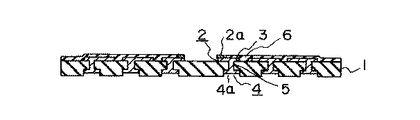
図1は本発明の第1の実施の形態に係る半導体装置用基板の構成を示す断面図である。この半導体装置用基板は、液状樹脂が硬化されてなる絶縁層1と、絶縁層1の一方の面に形成され、半導体チップに接続可能に配置された複数の接続電極2と、絶縁層1の一方の面に形成され、各接続電極2に個別に接続された複数の配線領域3と、表面が絶縁層1に被覆されずに絶縁層1の表面よりも凹んだ位置にあり、かつ側面が絶縁層1に被覆されるように絶縁層1の他方の面内に形成され、外部要素に接続可能に配置された複数のランド電極4と、各ランド電極4と各配線領域2とを個別に接続する複数のバイア5とを備えている。
【0042】
また、各配線領域3及び絶縁層1からなる面は、接続電極2上を除き、保護層6にて覆われている。
ここで、絶縁層1は、液状の絶縁樹脂の塗布、乾燥により形成される。絶縁樹脂としては、エポキシ樹脂系、アクリル樹脂系の絶縁樹脂等が適用可能となっている。
【0043】
各接続電極2は、半導体チップに良好に接続するためのめっき層2aが表面に形成されている。めっき層2aは、導電層(銅層)上の下地がNi層であり、Ni層上にAu層が形成されてなる。
【0044】
各ランド電極4は、エッチングストッパ層としてのはんだ層4aが表面に形成され、はんだ層4aの一部又は全部が除去されると、図2に示すように、表面が絶縁層1に被覆されずに絶縁層1の表面よりも凹んだ位置にあり、かつ側面が絶縁層1に被覆されるように絶縁層1の他方の面内に形成される。
【0045】
次に、このような半導体装置用基板の製造方法について説明する。
始めに、シート状の0.2mm厚の銅合金10が洗浄される。乾燥後、この銅合金10の裏面には、全域に耐酸性テープとしてのドライフィルム(図示せず)が貼着される。しかる後、この銅合金10の表面には、スクリーン印刷により、絶縁層1となる感光性絶縁樹脂(DPR−105;商品名:(株)アサヒ化学研究所製)が印刷される。
【0046】
この感光性絶縁樹脂は、ランド電極4の形成位置に対応するパターンが露光され、現像されることにより、ランド電極4の形成位置の絶縁層が穴径0.6mmで除去され、もって、図3(a)に示すように、20μm厚の絶縁層1aが選択的に形成される。
【0047】
続いて、銅合金10を電極として電解ニッケルめっき工程が実行され、図3(b)に示すように、絶縁層1aに囲まれた銅合金10部分に、5μm厚のはんだ層4aが形成される。はんだ層4aは、最終工程の銅合金10エッチング除去時のストッパー層となるものであるため、ピンホールの無いように、また十分にエッチング耐性を有するように、厚さ1μmから10μm程度、特に2μmから8μm程度に形成されることが好ましい。
【0048】
また、このような銅合金10は、硫酸銅めっき液に浸漬され、電解銅めっき工程が施されることにより、図3(c)に示すように、10μm厚の銅層11が形成される。
【0049】
再び、スクリーン印刷により、絶縁層1となる感光性絶縁樹脂が印刷される。この絶縁樹脂は、各ランド電極表面のはんだ層4aを一部露出させるパターンに対応して露光され、現像されることにより、ランド電極4の形成位置における中央部の絶縁層が穴径0.08mmで除去されてバイアホール12が形成され、もって、図4(a)に示すように、20μm厚の絶縁層1aとあわせて40μm厚の絶縁層1が形成される。
【0050】
次に、銅合金10を電極として電解銅めっき工程が施され、20μm厚の銅めっき層がバイアホール12内に形成され、もって、バイアホール12内が銅層で充填されてバイア5が形成される。しかる後、バイアホール12上面及び絶縁層1表面がバフ研磨されて平滑化される。
【0051】
続いて、全面に無電解銅めっきが厚さ0.5μmで施され、電解めっきが厚さ10μmで施されることにより、全面に10.5μm厚の銅層が形成される。
さらに、感光性の液状レジスト(PMER;商品名:東京応化工業(株)製)が浸漬により、両面に10μm厚で塗布される。この液状レジストは、接続電極2及び配線領域3を形成するパターンに対応して露光され、現像されてパタ−ニングされる。
【0052】
しかる後、銅層が選択的にエッチングされて除去され、また裏面のレジストがドライフィルムごと剥離され、もって、図4(b)に示すように、接続電極2及び配線領域3が形成された構造となる。
【0053】
配線領域3上に、保護層6として、絶縁樹脂と同材質の樹脂がスクリーン印刷され、半導体チップとの接続電極2を露出させるパターンに対応し露光され、現像されて、接続電極2上の樹脂が除去される。
【0054】
また、接続電極2上に、無電解めっきにより、ニッケルめっきが厚さ2μm、金めっきが厚さ0.3μmで施される。すなわち、図4(c)に示すように、接続電極2上に、Ni層及びAu層からなるめっき層2aが形成される。なお、この図4(c)に示す構造は、出荷可能な半導体装置用基板となっている。
【0055】
続いて、保護層6、配線領域3及び接続電極2からなる回路形成面に保護用のドライフィルムが貼着され(図示せず)、しかる後、銅合金10が過硫酸アンモニウムを用いて、エッチングにより除去される。このとき、はんだ層4aがエッチングストッパ層となり、図4(d)に示すように、銅合金10のみが除去される。続いて、図4(e)に示すように、はんだ層4aが剥離除去され、ドライフィルムが剥離され、半導体装置用基板が完成される。
【0056】
上述したように第1の実施の形態によれば、絶縁層1が液状樹脂から形成されるため、ドリルによる穴あけ工程を省略できることから高密度なパターンと薄型の形状を実現できると共に、高い平滑性をもつ実装面を実現でき、さらに、各ランド電極4の表面が絶縁層1の表面よりも凹んだ位置にあるようにしたので、導電性ボールを各ランド電極4上に形成するとき及び導電性ボールを形成した半導体装置を外部要素に搭載するときに、突出した絶縁層1表面がダムとして作用するので、接続用のはんだの量を適切に制御することができ、はんだブリッジによる回路の短絡等の不良が発生しにくく、もって、実装の確実性の向上を期待することができる。
【0057】
また、シート状の銅合金10上にビルドアップし、その後銅合金10を除去するため、高い平滑性を有する絶縁層1を実現でき、また、薄型化された場合でも容易に、高い信頼性で製造することができる。
【0058】
さらに、各ランド電極4の表面がエッチングストッパ層として機能する材料により形成されるので、上述した効果を容易かつ確実に奏することができる。
また、製造工程としては、シート状の銅合金10上に、選択的に絶縁層1aを形成し、しかる後、各ランド電極4の表面となるはんだ層4aを形成し、以下、順次、ランド電極4を形成し、再度絶縁層1を形成し、各バイア5、各配線領域3及び各接続電極2を形成し、銅合金10をエッチングにより除去し、はんだ層4aを除去するので、上述した効果を奏する半導体装置用基板を容易かつ確実に製造することができ、製造工程の安定性を向上させることができる。
【0059】
さらに、高精度で厚さを制御し易いはんだ層4aを設け、しかる後、はんだ層4aを除去するので、ランド電極4の凹み量を容易に制御でき、もって、実装時のはんだ量も高精度に制御することができる。
(第2の実施の形態)
次に、本発明の第2の実施の形態に係る半導体装置用基板について図1を用いて説明する。
【0060】
すなわち、本実施の形態に係る半導体装置用基板は、第1の実施形態の製造方法を変形させたものであり、各ランド電極4におけるはんだ層4aを形成した後に絶縁層1を形成する製造方法であって、完成品の構造としては図1に示した構造と同一構造となっている。
【0061】
次に、このような半導体装置用基板の製造方法について説明する。
始めに、シート状の0.2mm厚の銅合金10が洗浄される。乾燥後、この銅合金10の裏面には、図示しないドライフィルムが貼着される。しかる後、この銅合金10の表面には、浸漬により、感光性の液状レジスト(PMER;商品名:東京応化工業(株)製)が25μm厚で塗布される。なお、液状レジストの塗布厚は、後に形成するランド電極4の厚さよりも厚いことが必要であり、例えば25〜50μm程度が好ましい。
【0062】
この液状レジストは、ランド電極4の形成位置のパターンに対応して露光され、現像されることにより、ランド電極4の形成位置の部分が穴径0.6mmで除去され、もって、図5(a)に示すように、20μm厚のレジスト層13が選択的に形成される。
【0063】
続いて、銅合金10を電極として電解はんだめっきが施され、図5(b)に示すように、レジスト層13に囲まれた銅合金10部分に、10μm厚のはんだ層4bが形成される。はんだ層4aは、最終工程の銅合金10エッチング除去時のストッパー層となるものであるため、ピンホールの無いように、また十分にエッチング耐性を有するように、さらに、後にエッチングによってその一部を除去するため、厚さは、5μmから15μm程度が好ましく、特に8μmから10μm程度に形成されることが好ましい。
【0064】
なお、このはんだ層4a上に電解銅めっきを施し、15μm厚程度の銅層を形成し、ランド電極4を補強してもよい。
次に、図5(c)に示すように、レジスト13が剥離される。
【0065】
続いて前述同様に、スクリーン印刷により、絶縁層1となる感光性絶縁樹脂(DPR−105;商品名:(株)アサヒ化学研究所製)が印刷される。この絶縁樹脂は、各ランド電極4を一部露出させるパターンに対応して露光され、現像されることにより、ランド電極4の形成位置における中央部の絶縁層が穴径0.08mmで除去されてバイアホール12が形成され、図5(d)に示すように、40μm厚の絶縁層1が形成される。
【0066】
銅合金10を電極として電解銅めっきが施され、20μm厚の銅めっき層がバイアホール12内に形成され、もって、バイアホール12内が銅層で充填されてバイア5が形成される。しかる後、バイアホール12上面及び絶縁層1表面がバフ研磨されて平滑化される。
【0067】
続いて、全面に無電解めっきが厚さ0.5μmで施され、電解めっきを厚さ10μmで施されることにより、全面に10.5μm厚の銅層が形成される。
さらに、感光性の液状レジスト(PMER)が浸漬により、両面に厚さ10μmで塗布される。この液状レジストは、接続電極2及び配線領域3を形成するパターンに対応して露光され、現像されてパターニングされる。
【0068】
しかる後、塩化第二鉄を用いたエッチングにより、銅層が選択的に除去され、また、裏面のレジストがドライフィルムごと剥離され、もって、図5(e)に示すように、接続電極2及び配線領域3が形成された構造となる。
【0069】
配線領域3上に、保護層6として、絶縁樹脂と同材質の樹脂がスクリーン印刷され、半導体チップとの接続電極2を露出させるパターンに対応し露光され、現像されて、接続電極2上の樹脂が除去される。
【0070】
また、接続電極2上に、無電解めっきにより、ニッケルめっきが厚さ2μm、金めっきが厚さ0.3μmで施され、図5(f)に示すように、Ni層及びAu層からなるめっき層2aが形成される。なお、この図5(f)に示す構造は、出荷可能な半導体装置用基板となっている。
【0071】
続いて、保護層6、配線領域3及び接続電極2からなる回路形成面に保護用のドライフィルムが貼着され(図示略)、しかる後、銅合金10がエッチングにより除去される。このとき、はんだ層4aがエッチングストッパ層となり、図5(g)に示すように、銅合金のみが除去される。また、図5(h)に示すように、はんだ層4aが塩化第二鉄により5μmだけエッチングされ、ドライフィルムが剥離され、半導体装置用基板が完成される。
【0072】
上述したように第2の実施の形態によれば、第1の実施形態の効果に加え、製造工程としては、シート状の銅合金10上に、選択的にはんだ層4a及び各ランド電極4を形成し、しかる後、順次、絶縁層1を形成し、各バイア5、各配線領域3及び各接続電極2を形成し、銅合金10をエッチングにより除去し、はんだ層4aを一部除去するので、第1の実施形態の効果を奏する半導体装置用基板を容易かつ確実に製造することができ、製造工程の安定性を向上でき、さらに、選択的にはんだ層4aを形成する際に、高解像度なレジストを用いることにより、より一層高密度で微細なパターンを形成することができる。
(第3の実施の形態)
次に、本発明の第3の実施の形態に係る半導体装置について説明する。
【0073】
図6はこの半導体装置の構成を示す断面図であり、図1と同一部分には同一符号を付してその詳しい説明は省略し、ここでは異なる部分についてのみ述べる。
すなわち、本実施の形態に係る半導体装置は、第1又は第2の実施形態の変形形態であり、図1に示す装置に対し、図6に示すように、各接続電極2に電気的に接続された半導体チップ21と、各ランド電極4に個別に形成された複数の導電性ボール22とを備え、少なくとも半導体チップ21とその各接続電極2への接続部とが絶縁樹脂23により封止されて形成されている。
【0074】
なお、第1の実施の形態における図4(c)と、第2の実施の形態における図5(f)とは互いに同一内容の工程のため、ここでは図4(c)の工程のみを例に挙げ、その後工程を続けるように本実施の形態を説明する。
【0075】
次に、このような半導体装置の製造方法について説明する。
図4(c)に示す工程の後、基板中央の半導体チップ搭載部に半導体チップ21が搭載され、図7(a)に示すように、半導体チップ21と接続電極2とがボンディングワイヤ24を介して接続される。
【0076】
続いて、この半導体チップの搭載面は、図7(b)に示すように、エポキシ樹脂等の絶縁樹脂23で封止される。
さらに、図7(c)に示すように、銅合金10がエッチングにより除去される。このとき、ランド電極4のはんだ層4aがエッチングストッパーとなるため、ランド電極4内部やバイア5等は除去されず、銅合金10のみが除去される。
【0077】
しかる後、図7(d)に示すように、はんだ層4aが剥離除去され、さらに、図7(e)に示すように、各ランド電極4に導電性ボール22が形成される。これにより、半導体装置が完成される。
【0078】
上述したように第3の実施の形態によれば、第1の実施形態に係る半導体装置用基板に半導体チップ21が接続され、かつ半導体チップ21とその接続部とが樹脂封止されているので、第1の実施形態の作用効果により、高密度化並びに薄型化を期待でき、もって、高機能化を期待することができる。
【0079】
また、製造工程としては始めから述べると、シート状の銅合金10上に、選択的に絶縁層1aを形成し、しかる後、各ランド電極4の表面となるはんだ層4aを形成し、以下、順次、ランド電極4を形成し、再度絶縁層1を形成し、各バイア5、各配線領域3及び各接続電極2を形成し、各接続電極2に半導体チップ21を接続し、半導体チップ21等を樹脂封止し、銅合金10をエッチングにより除去し、はんだ層4aを剥離除去し、各ランド電極4に導電性ボール22を形成するので、上述した作用効果を奏する半導体装置を容易かつ確実に製造することができ、製造工程の安定性を向上させることができる。
【0080】
なお、本実施の形態では詳述を避けたが、図5(f)の後工程を続けて半導体装置を製造する場合、製造工程としては始めから述べると、シート状の銅合金10上に、選択的にはんだ層4a及び各ランド電極4を形成し、しかる後、順次、絶縁層1を形成し、各バイア5、各配線領域3及び各接続電極2を形成し、各接続電極2に半導体チップ21を接続し、半導体チップ21等を樹脂封止し、銅合金10をエッチングにより除去し、はんだ層4aを一部除去し、各ランド電極4(はんだ層4a)上に導電性ボール22を形成するので、本実施形態の作用効果を奏する半導体装置を容易かつ確実に製造することができ、製造工程の安定性を向上でき、さらに、選択的にはんだ層4aを形成する際に、高解像度なレジストを用いることにより、より一層高密度で微細なパターンを形成することができる。
(他の実施の形態)
なお、上記第3の実施の形態では、図4(c)又は図5(f)に示す工程の後に半導体チップ21を搭載して最後に銅合金10を除去することにより半導体装置を製造する場合について説明したが、これに限らず、図4(e)又は図5(h)に示すはんだ層4aの除去工程の後、半導体チップ21と接続電極2とがボンディングワイヤ24を介して接続される工程と、半導体チップ21の搭載面が絶縁樹脂23で封止される工程と、ランド電極4に導電性ボール22が形成される工程とを付加することにより、図6に示す構造の半導体装置を製造しても、本発明を同様に実施して同様の効果を得ることができる。
その他、本発明はその要旨を逸脱しない範囲で種々変形して実施できる。
【0081】
【発明の効果】
以上説明したように請求項1,3の発明により製造される半導体装置用基板によれば、絶縁層が液状樹脂から形成されるため、ドリルによる穴あけ工程を省略できることから高密度なパターンと薄型の形状を実現でき、また、高い平滑性をもつ実装面を実現でき、さらに、各ランド電極の表面が絶縁層の表面よりも凹んだ位置にあるようにしたので、導電性ボールを各ランド電極上に形成するとき及び導電性ボールを形成した半導体ボールを外部要素に搭載するときに、突出した導電層表面がダムとして作用するので、接続用のはんだの量を適切に制御することができ、もって、実装の確実性の向上を期待できる半導体装置用基板を提供できる。
【0082】
また、請求項2,4の発明により製造される半導体装置によれば、請求項1,3の発明により製造される半導体装置用基板に半導体チップが接続され、かつ半導体チップとその接続部とが樹脂封止され、各ランド電極には導電性ボールが形成されたので、請求項1,3の発明により製造される半導体装置用基板と同様の効果を奏する半導体装置を提供できる。
【0083】
さらに、請求項1の発明は、シート状の金属材料上に、各ランド電極の形成位置とは異なる位置に選択的に絶縁層を形成し、しかる後、各ランド電極の表面となるエッチングストッパ層を形成し、以下、順次、ランド電極を形成し、再度絶縁層を形成し、各バイア、各配線領域及び各接続電極を形成し、金属材料をエッチングにより除去し、エッチングストッパ層の少なくとも表面を除去するので、請求項1,3の発明により製造される半導体装置用基板の効果を前述したが、この前述した効果を奏する半導体装置用基板を容易かつ確実に製造することができ、製造工程の安定性を向上できる半導体装置用基板を提供できる。
【0084】
さらに、請求項2の発明は、シート状の金属材料上に、選択的に絶縁層を形成し、しかる後、各ランド電極の表面となるエッチングストッパ層を形成し、以下、順次、ランド電極を形成し、再度絶縁層を形成し、各バイア、各配線領域及び各接続電極を形成し、各接続電極に半導体チップを接続し、半導体チップ等を樹脂封止し、金属材料をエッチングにより除去し、エッチングストッパ層の少なくとも表面を除去するので、請求項2,4の発明により製造される半導体装置の効果を前述したが、この前述した効果を奏する半導体装置を容易かつ確実に製造することができ、製造工程の安定性を向上させることができる。
【0085】
さらに、請求項3の発明は、シート状の金属材料上に、選択的にエッチングストッパ層及び各ランド電極を形成し、しかる後、順次、絶縁層を形成し、各バイア、各配線領域及び各接続電極を形成し、金属材料をエッチングにより除去し、エッチングストッパ層の少なくとも表面を除去するので、請求項1,3の発明により製造される半導体装置用基板の効果を前述したが、この前述した効果を奏する半導体装置用基板を容易かつ確実に製造することができ、製造工程の安定性を向上させることができ、製造工程の安定性を向上でき、さらに、選択的にエッチングストッパ層を形成する際に、高解像度なレジストを用いることにより、より高密度で微細なパターンを形成できる半導体装置用基板を提供できる。
【0086】
さらに、請求項4の発明は、シート状の金属材料上に、選択的にエッチングストッパ層及び各ランド電極を形成し、しかる後、順次、絶縁層を形成し、各バイア、各配線領域及び各接続電極を形成し、各接続電極に半導体チップを接続し、半導体チップ等を樹脂封止し、金属材料をエッチングにより除去し、エッチングストッパ層の少なくとも表面を除去するので、請求項2,4の発明により製造される半導体装置の効果を前述したが、この前述した効果を奏する半導体装置を容易かつ確実に製造することができ、製造工程の安定性を向上でき、さらに、選択的にエッチングストッパ層を形成する際に、高解像度なレジストを用いることにより、より一層高密度で微細なパターンを形成できる半導体装置を提供できる。
【図面の簡単な説明】
【図1】本発明の第1の実施の形態に係る半導体装置用基板の構成を示す断面図
【図2】同実施の形態におけるランド電極の概略構成を説明するための斜視図
【図3】同実施の形態における製造方法を説明するための工程断面図
【図4】同実施の形態における製造方法を説明するための工程断面図
【図5】本発明の第2の実施の形態における製造方法を説明するための工程断面図
【図6】本発明の第3の実施の形態に係る半導体装置の構成を示す断面図
【図7】同実施の形態における製造方法を説明するための工程断面図
【図8】従来の半導体装置用基板を用いた半導体装置の構成を示す断面図
【図9】従来の半導体装置用基板を用いた半導体装置の一部を拡大して示す断面図
【符号の説明】
1,1a…絶縁層
2…接続電極
2a…めっき層
3…配線領域
4…ランド電極
4a…はんだ層
5…バイア
6…保護層
10…銅合金
11…銅層
12…バイアホール
13…レジスト層
21…半導体チップ
22…導電性ボール
23…絶縁樹脂
24…ボンディングワイヤ[0001]
BACKGROUND OF THE INVENTION
The present invention relates to a BGA (Ball Grid Array) type semiconductor device substrate on which a semiconductor chip is mounted. Manufacturing method and Semiconductor equipment Set In particular, a semiconductor device substrate that is related to a manufacturing method and that can prevent a short circuit due to a solder bridge, etc. Manufacturing method and Semiconductor equipment Set It relates to a manufacturing method.
[0002]
[Prior art]
Recently, portable electronic devices such as notebook computers, handy video devices, and mobile phones have been widely sold. For this reason, there is an increasing demand for downsizing and higher functionality of a semiconductor device substrate when the semiconductor device is mounted in these electronic devices.
[0003]
Such a substrate for a semiconductor device includes a BGA type substrate on which a semiconductor chip such as an LSI can be mounted. Specifically, for example, a substrate disclosed in Japanese Patent Application Laid-Open No. 8-37345 is known. ing. Note that a semiconductor device that can be mounted on a mother board or the like of an external element is manufactured by mounting a semiconductor chip on a semiconductor device substrate and sealing with resin.
[0004]
FIG. 8 is a cross-sectional view showing a configuration of a semiconductor device using the semiconductor device substrate. In this semiconductor device, a copper-clad laminate for a printed wiring board is used as a
[0005]
Next, of the copper layers on both surfaces of the
[0006]
When a pattern that cannot be formed by a single layer is provided as the
[0007]
At this time, in order to establish conduction between the upper and
[0008]
In addition, after the formation of the
[0009]
Further, as shown in FIG. 9, a protective layer made of a solder resist 38 for protecting from the solder or the like is formed between the
[0010]
[Problems to be solved by the invention]
However, in the semiconductor device substrate as described above, a drilling process is performed on the
[0011]
The
[0012]
As shown in FIG. 9, the method of applying the solder resist 38 to the
[0013]
Furthermore, the method of applying the solder resist 38 on the
[0014]
The present invention has been made in view of the above circumstances, and can realize a mounting surface having high density and thinness and high smoothness, and can improve mounting reliability. Manufacturing method and Semiconductor equipment Set It relates to a manufacturing method.
[0015]
[Means for Solving the Problems]
The invention corresponding to claim 1 Liquid An insulating layer formed by curing a resin, a plurality of connection electrodes formed on one surface of the insulating layer and arranged to be connectable to a semiconductor chip, and formed on one surface of the insulating layer, and each of the connections A plurality of wiring regions individually connected to the electrodes, and the insulating layer so that the surface is not covered with the insulating layer but is recessed from the surface of the insulating layer, and the side surface is covered with the insulating layer. A semiconductor device substrate comprising a plurality of land electrodes formed in the other surface of the layer and arranged to be connectable to an external element, and vias that individually connect the land electrodes and the wiring regions. In the manufacturing method, on the sheet-like metal material, selectively at a position different from the formation position of each land electrode. Apply and cure liquid resin A first insulating layer forming step for forming an insulating layer; and a stopper layer for selectively forming a plurality of etching stopper layers on the surface of the land electrodes on the metal material and surrounded by the insulating layer A land forming step of forming the land electrodes on the etching stopper layers by plating, an upper portion of the land electrodes and an upper portion of the insulating layer so as to partially expose the land electrodes. In Apply and cure liquid resin A second insulating layer forming step for forming an insulating layer; a wiring forming step for forming each via, each wiring region and each connection electrode by plating; an etching step for removing the metal material by etching; And a stopper layer removing step for removing at least the surface of the etching stopper layer.
[0016]
The invention corresponding to
[0019]
Furthermore, the invention corresponding to claim 3 is: Liquid An insulating layer formed by curing a resin, a plurality of connection electrodes formed on one surface of the insulating layer and arranged to be connectable to a semiconductor chip, and formed on one surface of the insulating layer, and each of the connections A plurality of wiring regions individually connected to the electrodes, and the insulating layer so that the surface is not covered with the insulating layer but is recessed from the surface of the insulating layer, and the side surface is covered with the insulating layer. A semiconductor device substrate comprising a plurality of land electrodes formed in the other surface of the layer and arranged to be connectable to an external element, and vias that individually connect the land electrodes and the wiring regions. In the manufacturing method, on the sheet-like metal material, a stopper layer forming step of selectively forming a plurality of etching stopper layers on the surface of each land electrode at the formation position of each land electrode; etching And the land forming step of forming the respective land electrodes on the stopper layer, wherein to expose a portion of each land electrode, wherein the upper portion of the upper and the metal material of each land electrode Apply and cure liquid resin An insulating layer forming step for forming an insulating layer; a wiring forming step for forming each via, each wiring region and each connection electrode by plating; an etching step for removing the metal material by etching; and the etching stopper. And a stopper layer removing step for removing at least the surface of the layer.
[0020]
The invention corresponding to claim 4 is: Liquid An insulating layer formed by curing a resin, a plurality of connection electrodes formed on one surface of the insulating layer and arranged to be connectable to a semiconductor chip, and formed on one surface of the insulating layer, and each of the connections A plurality of wiring regions individually connected to the electrodes, and the insulating layer so that the surface is not covered with the insulating layer but is recessed from the surface of the insulating layer, and the side surface is covered with the insulating layer. A semiconductor device substrate comprising a plurality of land electrodes formed in the other surface of the layer and arranged to be connectable to an external element; and vias that individually connect the land electrodes and the wiring regions; A semiconductor chip electrically connected to each connection electrode, and a plurality of conductive balls individually formed on each land electrode, and at least the semiconductor chip and a connection portion to each connection electrode; Is half sealed with resin In a manufacturing method of a body device, a stopper layer forming step of selectively forming a plurality of etching stopper layers on the surface of each land electrode on the land electrode forming position on a sheet-like metal material, and plating A land forming step for forming each land electrode on each etching stopper layer; and a portion of the land electrode so as to partially expose the land electrode and an upper portion of the metal material. Apply and cure liquid resin An insulating layer forming step for forming an insulating layer; a wiring forming step for forming each via, each wiring region and each connection electrode by plating; and a chip connecting step for connecting a semiconductor chip to each connection electrode; A resin sealing step for resin sealing at least the semiconductor chip and its connection portions to the connection electrodes; an etching step for removing the metal material by etching; and a stopper layer for removing at least the surface of the etching stopper layer A method for manufacturing a semiconductor device includes a removing step and a step of individually forming a conductive ball on each land electrode.
(the term)
Next, a supplementary description will be given of the materials applied to the present invention as described above.
[0021]
The insulating layer is formed by curing a liquid resin applied by screen printing or curtain coating. As the liquid resin, an epoxy resin, a polyimide resin, an acrylic resin, or the like is applicable. In addition, as the liquid resin, it is preferable to use a photosensitive resin from the viewpoint of easily processing via holes and the like with high accuracy. However, even if a non-photosensitive resin is used, it can be formed into a desired shape by fine processing using an excimer laser or the like.
[0022]
The insulating layer covers the side surface of the land electrode, the surface projects downward from the surface of the land electrode, and has an opening having substantially the same size as the land electrode.
Further, the substrate for a semiconductor device may have either a structure capable of mounting one semiconductor chip or a structure capable of mounting two or more semiconductor chips.
[0023]
Further, the substrate for a semiconductor device may have a multilayer structure in which the printed circuit portion has the number of layers required for wiring, for example, a power supply layer and a ground layer are provided.
The etching stopper layer serves as a stopper when the sheet-like metal material is removed by etching. For example, the metal material is copper, and a persulfate etching solution such as ammonium persulfate or potassium persulfate, or a copper ammonium complex ion is mainly used. When an etching solution made of an alkaline aqueous solution as a component is used, solder or the like is used.
[0024]
The material of the etching stopper layer is preferably one that has a strong adhesion to the wiring material and is not easily corroded by the etching solution, and can be easily formed on a metal material. Specifically, it is appropriately selected depending on the relationship between the metal material and the etching solution.
[0025]
Further, at least the surface of the etching stopper layer is removed after the metal material is etched. For this reason, it is preferable that it is a material which can be etched or removed by a liquid different from the etching liquid for the metal material. In addition, after removing at least the surface of the etching stopper layer, the surface protective layer may be formed of a metal such as Au or Pd with a thickness smaller than the removed thickness.
[0026]
Here, when removing the surface of the etching stopper layer, the amount of depression of the land electrode can be appropriately controlled by controlling the amount of etching. Further, when removing the etching stopper layer, the dent amount of the land electrode can be appropriately controlled by controlling the formation thickness of the etching stopper layer. Unlike the conventional solder resist thickness control, such a control method can be controlled with high accuracy. In particular, the method of completely removing the etching stopper layer is preferable because the thickness of formation of the etching stopper layer such as the plating amount can be controlled with high accuracy.
[0027]
The material of the etching stopper layer is preferably a material having high wettability relative to a material (for example, solder) used for connection to a printed wiring board or the like of an external element.
The method for forming the etching stopper layer includes plating, vapor deposition, sputtering, and the like, which can be selected as appropriate.
[0028]
Taking solder as an example, the solder can be easily formed by plating. If the metal material is a copper alloy, it is etched using an alkaline etchant mainly composed of a copper ammonium complex ion. Then, the copper alloy is etched and the solder layer becomes a stopper layer.
[0029]
As the sheet-like metal material, for example, copper, a copper alloy, or an iron-Ni alloy represented by 42 alloy (42 wt% Ni, balance Fe) can be used. This is preferable in that it has excellent thermal conductivity and low electrical resistance.
[0030]
The thickness of the sheet-like metal material is required to be thick enough to function as a support substrate and not so thick as to be easily removed by etching, for example, within a range of about 0.15 mm to 0.35 mm. It is preferable that it exists in. Moreover, although smoothness is calculated | required as a metal material, the grade of the smoothness which a normal metal material has may be sufficient.
[0031]
In the via formation step, filling the via hole by plating is preferable from the viewpoint of preventing the formation of bubbles in the via hole. Specifically, it is possible to perform electroplating in which a metal material is energized, and the via hole can be filled with a simple process.
[0032]
In the process of forming a conductor circuit composed of a wiring region and a connection electrode on a via, an electrolytic Cu plating such as a conventional subtractive method, a semi-additive method, or a full additive method can be applied, but a via is already formed. Therefore, a conductor circuit can be easily formed.
[0033]
As the subtractive method, for example, electroless plating or sputtering can be used. Specifically, for example, after forming a thin copper layer having a thickness of 0.2 μm, electrolytic copper plating having a thickness of 10 μm is applied to the entire surface. A resist (eg, PMER; trade name: manufactured by Tokyo Ohka Kogyo Co., Ltd.) is applied and dried, and then the steps of exposure, development, etching, and resist stripping are performed. Further, as the resist, a negative photosensitive resist is desirable. For example, a resist called a trade name PMER can be used. As a coating method, dipping, screen printing, spin coating, or the like can be used as appropriate.
[0034]
As a semi-additive method, for example, electroless plating or sputtering can be used. Specifically, for example, after forming a thin copper layer having a thickness of 0.2 μm, a resist (eg, PMER) is applied and dried. After that, exposure and development are performed, and electrolytic copper plating with a thickness of 10 μm is applied to the pattern region that becomes the wiring region and the connection electrode. Further, after the resist is removed, the thin copper layer is removed by etching.
[0035]
As a full additive method, for example, after applying a catalyst and forming a resist, a wiring region and a connection electrode are formed by electroless plating.
As a method for connecting the semiconductor chip to the semiconductor device substrate, there are wire bonding, bumps, and the like. Further, at least the semiconductor chip and the connection portion between the semiconductor chip and the semiconductor device substrate are sealed with resin, and then the metal material is etched.
(Function)
Therefore, the substrate for a semiconductor device manufactured by the invention corresponding to
[0036]
[0037]
And claims 1 In the invention corresponding to the above, an insulating layer is selectively formed on a sheet-like metal material at a position different from the position where each land electrode is formed, and then an etching stopper layer serving as the surface of each land electrode is formed. In the following, land electrodes are formed one after another, insulating layers are formed again, each via, each wiring region and each connection electrode are formed, the metal material is removed by etching, and at least the surface of the etching stopper layer is removed. ,
[0038]
And claims 2 In the invention corresponding to the above, an insulating layer is selectively formed on a sheet-like metal material, and then an etching stopper layer to be the surface of each land electrode is formed. An insulating layer is formed again, each via, each wiring region and each connection electrode are formed, a semiconductor chip is connected to each connection electrode, the semiconductor chip is sealed with resin, a metal material is removed by etching, an etching stopper Since at least the surface of the layer is removed,
[0039]
And claims 3 In the invention corresponding to the above, an etching stopper layer and each land electrode are selectively formed on a sheet-like metal material, and then an insulating layer is sequentially formed, and each via, each wiring region, and each connection electrode are formed. Forming and removing the metal material by etching to remove at least the surface of the etching stopper layer. , 3 Corresponding to Of a semiconductor device substrate manufactured according to the invention Action As mentioned above, this mentioned above A semiconductor device substrate having an effect can be manufactured easily and reliably, the stability of the manufacturing process can be improved, the stability of the manufacturing process can be improved, and an etching stopper layer is selectively formed. At this time, by using a high-resolution resist, it is possible to form a finer pattern with higher density.
[0040]
And claims 4 In the invention corresponding to the above, an etching stopper layer and each land electrode are selectively formed on a sheet-like metal material, and then an insulating layer is sequentially formed, and each via, each wiring region, and each connection electrode are formed. The semiconductor chip is formed, connected to each connection electrode, the semiconductor chip or the like is resin-sealed, the metal material is removed by etching, and at least the surface of the etching stopper layer is removed. , 4 Corresponding to Of the semiconductor device manufactured by the invention Action As mentioned above, this mentioned above It is possible to easily and reliably manufacture a semiconductor device having an effect, improve the stability of the manufacturing process, and further, by using a high-resolution resist when selectively forming an etching stopper layer, A high-density and fine pattern can be formed.
[0041]
DETAILED DESCRIPTION OF THE INVENTION
Hereinafter, embodiments of the present invention will be described with reference to the drawings.
(First embodiment)
FIG. 1 is a cross-sectional view showing a configuration of a substrate for a semiconductor device according to a first embodiment of the present invention. The substrate for a semiconductor device includes an insulating layer 1 formed by curing a liquid resin, a plurality of
[0042]
Further, the surface formed of each
Here, the insulating layer 1 is formed by applying and drying a liquid insulating resin. As the insulating resin, an epoxy resin-based or acrylic resin-based insulating resin or the like can be applied.
[0043]
Each
[0044]
As for each
[0045]
Next, a method for manufacturing such a semiconductor device substrate will be described.
First, the sheet-like 0.2 mm
[0046]
The photosensitive insulating resin is exposed to a pattern corresponding to the formation position of the
[0047]
Subsequently, an electrolytic nickel plating process is performed using the
[0048]
Further, such a
[0049]
Again, the photosensitive insulating resin used as the insulating layer 1 is printed by screen printing. This insulating resin is exposed and developed in correspondence with a pattern that partially exposes the
[0050]
Next, an electrolytic copper plating process is performed using the
[0051]
Subsequently, electroless copper plating is applied to the entire surface with a thickness of 0.5 μm, and electrolytic plating is applied with a thickness of 10 μm to form a 10.5 μm thick copper layer on the entire surface.
Further, a photosensitive liquid resist (PMER; trade name: manufactured by Tokyo Ohka Kogyo Co., Ltd.) is applied by immersion to a thickness of 10 μm on both sides. The liquid resist is exposed, developed and patterned in correspondence with the pattern for forming the
[0052]
Thereafter, the copper layer is selectively etched and removed, and the resist on the back surface is peeled off together with the dry film, so that the
[0053]
Resin of the same material as the insulating resin is screen-printed on the
[0054]
On the
[0055]
Subsequently, a protective dry film is attached to the circuit forming surface composed of the
[0056]
As described above, according to the first embodiment, since the insulating layer 1 is formed from a liquid resin, a drilling step by a drill can be omitted, so that a high-density pattern and a thin shape can be realized and high smoothness can be achieved. In addition, since the surface of each
[0057]
Further, since build-up is performed on the sheet-
[0058]
Furthermore, since the surface of each
As a manufacturing process, the insulating layer 1a is selectively formed on the sheet-
[0059]
Furthermore, since the
(Second Embodiment)
Next, a semiconductor device substrate according to a second embodiment of the present invention will be described with reference to FIG.
[0060]
That is, the substrate for a semiconductor device according to the present embodiment is a modification of the manufacturing method of the first embodiment. The manufacturing method of forming the insulating layer 1 after forming the
[0061]
Next, a method for manufacturing such a semiconductor device substrate will be described.
First, the sheet-like 0.2 mm
[0062]
This liquid resist is exposed and developed in accordance with the pattern of the
[0063]
Subsequently, electrolytic solder plating is performed using the
[0064]
The
Next, as shown in FIG. 5C, the resist 13 is peeled off.
[0065]
Subsequently, in the same manner as described above, a photosensitive insulating resin (DPR-105; trade name: manufactured by Asahi Chemical Research Co., Ltd.) to be the insulating layer 1 is printed by screen printing. This insulating resin is exposed and developed corresponding to a pattern that partially exposes each
[0066]
Electrolytic copper plating is performed using the
[0067]
Subsequently, electroless plating is applied to the entire surface with a thickness of 0.5 μm, and electrolytic plating is applied with a thickness of 10 μm to form a copper layer with a thickness of 10.5 μm on the entire surface.
Furthermore, a photosensitive liquid resist (PMER) is applied to both surfaces with a thickness of 10 μm by dipping. This liquid resist is exposed, developed and patterned corresponding to a pattern for forming the
[0068]
Thereafter, the copper layer is selectively removed by etching using ferric chloride, and the resist on the back surface is peeled off together with the dry film. As shown in FIG. The
[0069]
Resin of the same material as the insulating resin is screen-printed on the
[0070]
On the
[0071]
Subsequently, a protective dry film is affixed to the circuit forming surface composed of the
[0072]
As described above, according to the second embodiment, in addition to the effects of the first embodiment, as a manufacturing process, the
(Third embodiment)
Next, a semiconductor device according to a third embodiment of the present invention will be described.
[0073]
FIG. 6 is a cross-sectional view showing the configuration of this semiconductor device. The same parts as those in FIG. 1 are denoted by the same reference numerals, and detailed description thereof is omitted. Only different parts will be described here.
That is, the semiconductor device according to the present embodiment is a modification of the first or second embodiment, and is electrically connected to each
[0074]
Note that FIG. 4C in the first embodiment and FIG. 5F in the second embodiment have the same contents, so only the process in FIG. 4C is taken as an example here. This embodiment will be described so as to continue the process thereafter.
[0075]
Next, a method for manufacturing such a semiconductor device will be described.
After the step shown in FIG. 4C, the
[0076]
Subsequently, the mounting surface of the semiconductor chip is sealed with an insulating
Further, as shown in FIG. 7C, the
[0077]
Thereafter, as shown in FIG. 7D, the
[0078]
As described above, according to the third embodiment, the
[0079]
As a manufacturing process, the insulating layer 1a is selectively formed on the sheet-
[0080]
Although detailed description is avoided in the present embodiment, when a semiconductor device is manufactured by continuing the post-process of FIG. 5F, the manufacturing process will be described from the beginning on the sheet-
(Other embodiments)
In the third embodiment, the semiconductor device is manufactured by mounting the
In addition, the present invention can be implemented with various modifications without departing from the gist thereof.
[0081]
【The invention's effect】
As described above, according to the semiconductor device substrate manufactured according to the inventions of
[0082]
[0083]
And claims 1 According to the present invention, an insulating layer is selectively formed on a sheet-like metal material at a position different from the position where each land electrode is formed, and then an etching stopper layer which becomes the surface of each land electrode is formed. Then, land electrodes are formed one after another, insulating layers are formed again, each via, each wiring region and each connection electrode are formed, the metal material is removed by etching, and at least the surface of the etching stopper layer is removed.
[0084]
And claims 2 In this invention, an insulating layer is selectively formed on a sheet-like metal material, and then an etching stopper layer to be the surface of each land electrode is formed. Thereafter, the land electrodes are sequentially formed and insulated again. Forming a layer, forming each via, each wiring region and each connection electrode, connecting a semiconductor chip to each connection electrode, resin-sealing the semiconductor chip, etc., removing the metal material by etching, and forming an etching stopper layer Since at least the surface is removed,
[0085]
And claims 3 In this invention, an etching stopper layer and each land electrode are selectively formed on a sheet-like metal material, and then an insulating layer is sequentially formed, and each via, each wiring region, and each connection electrode are formed. The metal material is removed by etching, and at least the surface of the etching stopper layer is removed. , 3 of Of a semiconductor device substrate manufactured according to the invention effect As mentioned above, this effect mentioned above Can be manufactured easily and reliably, the stability of the manufacturing process can be improved, the stability of the manufacturing process can be improved, and the etching stopper layer is selectively formed. In addition, by using a high-resolution resist, it is possible to provide a semiconductor device substrate capable of forming a finer pattern with higher density.
[0086]
And claims 4 In this invention, an etching stopper layer and each land electrode are selectively formed on a sheet-like metal material, and then an insulating layer is sequentially formed, and each via, each wiring region, and each connection electrode are formed. The semiconductor chip is connected to each connection electrode, the semiconductor chip or the like is resin-sealed, the metal material is removed by etching, and at least the surface of the etching stopper layer is removed. , 4 of Of the semiconductor device manufactured by the invention effect As mentioned above, this effect mentioned above Can be manufactured easily and reliably, the stability of the manufacturing process can be improved, and when a selective etching stopper layer is formed selectively, a higher resolution resist can be used. Form fine patterns with high density In success Can be provided.
[Brief description of the drawings]
FIG. 1 is a cross-sectional view showing a configuration of a substrate for a semiconductor device according to a first embodiment of the invention.
FIG. 2 is a perspective view for explaining a schematic configuration of a land electrode according to the embodiment;
3 is a process cross-sectional view for explaining the manufacturing method in the same embodiment; FIG.
FIG. 4 is a process sectional view for explaining the manufacturing method according to the embodiment;
FIG. 5 is a process cross-sectional view for explaining a manufacturing method according to a second embodiment of the present invention.
FIG. 6 is a cross-sectional view showing a configuration of a semiconductor device according to a third embodiment of the present invention.
FIG. 7 is a process cross-sectional view for explaining the manufacturing method in the same embodiment;
FIG. 8 is a cross-sectional view showing a configuration of a semiconductor device using a conventional substrate for a semiconductor device.
FIG. 9 is an enlarged cross-sectional view showing a part of a semiconductor device using a conventional semiconductor device substrate;
[Explanation of symbols]
1, 1a ... Insulating layer
2 ... Connection electrode
2a ... Plating layer
3 ... Wiring area
4 ... Land electrode
4a ... Solder layer
5 ... Bahia
6 ... Protective layer
10 ... Copper alloy
11 ... Copper layer
12 ... Bahia Hall
13 ... resist layer
21 ... Semiconductor chip
22 ... Conductive ball
23. Insulating resin
24. Bonding wire
Claims (4)
前記絶縁層の一方の面に形成され、半導体チップに接続可能に配置された複数の接続電極と、
前記絶縁層の一方の面に形成され、前記各接続電極に個別に接続された複数の配線領域と、
表面が前記絶縁層に被覆されずに前記絶縁層の表面よりも凹んだ位置にあり、かつ側面が前記絶縁層に被覆されるように前記絶縁層の他方の面内に形成され、外部要素に接続可能に配置された複数のランド電極と、
前記各ランド電極と前記各配線領域とを個別に接続するバイアとを備えた半導体装置用基板の製造方法において、
シート状の金属材料上に、前記各ランド電極の形成位置とは異なる位置に選択的に液状樹脂を塗布及び硬化させて絶縁層を形成する第1の絶縁層形成工程と、
前記金属材料上でかつ前記絶縁層に囲まれた部分に選択的に前記各ランド電極の表面となる複数のエッチングストッパ層を形成するストッパ層形成工程と、
めっきにより、前記各エッチングストッパ層上に前記各ランド電極を形成するランド形成工程と、
前記各ランド電極を一部露出させるように、前記各ランド電極の上部及び前記絶縁層の上部に液状樹脂を塗布及び硬化させて絶縁層を形成する第2の絶縁層形成工程と、
めっきにより、前記各バイア、前記各配線領域及び前記各接続電極を形成する配線形成工程と、
前記金属材料をエッチングにより除去するエッチング工程と、
前記エッチングストッパ層の少なくとも表面を除去するストッパ層除去工程と
を含んでいることを特徴とする半導体装置用基板の製造方法。 An insulating layer formed by curing a liquid resin;
A plurality of connection electrodes formed on one surface of the insulating layer and arranged to be connectable to a semiconductor chip;
A plurality of wiring regions formed on one surface of the insulating layer and individually connected to the connection electrodes;
The surface is not covered with the insulating layer and is recessed from the surface of the insulating layer, and the side surface is formed in the other surface of the insulating layer so as to be covered with the insulating layer, A plurality of land electrodes arranged to be connectable;
In a method for manufacturing a substrate for a semiconductor device, comprising a via for individually connecting each land electrode and each wiring region,
A first insulating layer forming step of forming an insulating layer by selectively applying and curing a liquid resin on a sheet-like metal material at a position different from the formation position of each land electrode;
A stopper layer forming step of selectively forming a plurality of etching stopper layers on the surface of each land electrode on a portion surrounded by the insulating layer on the metal material;
Land formation step of forming each land electrode on each etching stopper layer by plating,
A second insulating layer forming step of forming an insulating layer by applying and curing a liquid resin on an upper portion of each land electrode and an upper portion of the insulating layer so as to partially expose the land electrodes;
A wiring forming step of forming each via, each wiring region and each connection electrode by plating,
An etching step of removing the metal material by etching;
And a stopper layer removing step for removing at least the surface of the etching stopper layer.
前記絶縁層の一方の面に形成され、半導体チップに接続可能に配置された複数の接続電極と、
前記絶縁層の一方の面に形成され、前記各接続電極に個別に接続された複数の配線領域と、
表面が前記絶縁層に被覆されずに前記絶縁層の表面よりも凹んだ位置にあり、かつ側面が前記絶縁層に被覆されるように前記絶縁層の他方の面内に形成され、外部要素に接続可能に配置された複数のランド電極と、
前記各ランド電極と前記各配線領域とを個別に接続するバイアとを備えた半導体装置用基板と、
前記各接続電極に電気的に接続された半導体チップと、
前記各ランド電極に個別に形成された複数の導電性ボールとを備え、
少なくとも前記半導体チップとその前記各接続電極への接続部とが樹脂封止されてなる半導体装置の製造方法において、
シート状の金属材料上に、前記各ランド電極の形成位置とは異なる位置に選択的に液状樹脂を塗布及び硬化させて絶縁層を形成する第1の絶縁層形成工程と、
前記金属材料上でかつ前記絶縁層に囲まれた部分に選択的に前記各ランド電極の表面となる複数のエッチングストッパ層を形成するストッパ層形成工程と、
めっきにより、前記各エッチングストッパ層上に前記各ランド電極を形成するランド形成工程と、
前記各ランド電極を一部露出させるように、前記各ランド電極の上部及び前記絶縁層の上部に液状樹脂を塗布及び硬化させて絶縁層を形成する第2の絶縁層形成工程と、
めっきにより、前記各バイア、前記各配線領域及び前記各接続電極を形成する配線形成工程と、
前記各接続電極に半導体チップを接続するチップ接続工程と、
少なくとも前記半導体チップとその前記各接続電極への接続部とを樹脂封止する樹脂封止工程と、
前記金属材料をエッチングにより除去するエッチング工程と、
前記エッチングストッパ層の少なくとも表面を除去するストッパ層除去工程と、
前記各ランド電極に個別に導電性ボールを形成する工程と
を含んでいることを特徴とする半導体装置の製造方法。 An insulating layer formed by curing a liquid resin;
A plurality of connection electrodes formed on one surface of the insulating layer and arranged to be connectable to a semiconductor chip;
A plurality of wiring regions formed on one surface of the insulating layer and individually connected to the connection electrodes;
The surface is not covered with the insulating layer and is recessed from the surface of the insulating layer, and the side surface is formed in the other surface of the insulating layer so as to be covered with the insulating layer, A plurality of land electrodes arranged to be connectable;
A substrate for a semiconductor device comprising vias for individually connecting the land electrodes and the wiring regions;
A semiconductor chip electrically connected to each of the connection electrodes;
A plurality of conductive balls individually formed on each land electrode,
In the method of manufacturing a semiconductor device in which at least the semiconductor chip and the connection portions to the connection electrodes are resin-sealed,
A first insulating layer forming step of forming an insulating layer by selectively applying and curing a liquid resin on a sheet-like metal material at a position different from the formation position of each land electrode;
A stopper layer forming step of selectively forming a plurality of etching stopper layers on the surface of each land electrode on a portion surrounded by the insulating layer on the metal material;
Land formation step of forming each land electrode on each etching stopper layer by plating,
A second insulating layer forming step of forming an insulating layer by applying and curing a liquid resin on an upper portion of each land electrode and an upper portion of the insulating layer so as to partially expose the land electrodes;
A wiring forming step of forming each via, each wiring region and each connection electrode by plating,
A chip connection step of connecting a semiconductor chip to each of the connection electrodes;
A resin sealing step of resin-sealing at least the semiconductor chip and the connection portions to the connection electrodes;
An etching step of removing the metal material by etching;
A stopper layer removing step for removing at least the surface of the etching stopper layer;
And a step of individually forming conductive balls on each land electrode.
前記絶縁層の一方の面に形成され、半導体チップに接続可能に配置された複数の接続電極と、
前記絶縁層の一方の面に形成され、前記各接続電極に個別に接続された複数の配線領域と、
表面が前記絶縁層に被覆されずに前記絶縁層の表面よりも凹んだ位置にあり、かつ側面が前記絶縁層に被覆されるように前記絶縁層の他方の面内に形成され、外部要素に接続可能に配置された複数のランド電極と、
前記各ランド電極と前記各配線領域とを個別に接続するバイアとを備えた半導体装置用基板の製造方法において、
シート状の金属材料上に、前記各ランド電極の形成位置に選択的に前記各ランド電極の表面となる複数のエッチングストッパ層を形成するストッパ層形成工程と、
めっきにより、前記各エッチングストッパ層上に前記各ランド電極を形成するランド形成工程と、
前記各ランド電極を一部露出させるように、前記各ランド電極の上部及び前記金属材料の上部に液状樹脂を塗布及び硬化させて絶縁層を形成する絶縁層形成工程と、
めっきにより、前記各バイア、前記各配線領域及び前記各接続電極を形成する配線形成工程と、
前記金属材料をエッチングにより除去するエッチング工程と、
前記エッチングストッパ層の少なくとも表面を除去するストッパ層除去工程と
を含んでいることを特徴とする半導体装置用基板の製造方法。 An insulating layer formed by curing a liquid resin;
A plurality of connection electrodes formed on one surface of the insulating layer and arranged to be connectable to a semiconductor chip;
A plurality of wiring regions formed on one surface of the insulating layer and individually connected to the connection electrodes;
The surface is not covered with the insulating layer and is recessed from the surface of the insulating layer, and the side surface is formed in the other surface of the insulating layer so as to be covered with the insulating layer, A plurality of land electrodes arranged to be connectable;
In a method for manufacturing a substrate for a semiconductor device, comprising a via for individually connecting each land electrode and each wiring region,
A stopper layer forming step of selectively forming a plurality of etching stopper layers on the surface of each land electrode on the sheet-like metal material at the formation position of each land electrode;
Land formation step of forming each land electrode on each etching stopper layer by plating,
An insulating layer forming step of forming an insulating layer by applying and curing a liquid resin on the upper portion of each land electrode and the upper portion of the metal material so as to partially expose the land electrodes;
A wiring forming step of forming each via, each wiring region and each connection electrode by plating,
An etching step of removing the metal material by etching;
And a stopper layer removing step for removing at least the surface of the etching stopper layer.
前記絶縁層の一方の面に形成され、半導体チップに接続可能に配置された複数の接続電極と、
前記絶縁層の一方の面に形成され、前記各接続電極に個別に接続された複数の配線領域と、
表面が前記絶縁層に被覆されずに前記絶縁層の表面よりも凹んだ位置にあり、かつ側面が前記絶縁層に被覆されるように前記絶縁層の他方の面内に形成され、外部要素に接続可能に配置された複数のランド電極と、
前記各ランド電極と前記各配線領域とを個別に接続するバイアとを備えた半導体装置用基板と、
前記各接続電極に電気的に接続された半導体チップと、
前記各ランド電極に個別に形成された複数の導電性ボールとを備え、
少なくとも前記半導体チップとその前記各接続電極への接続部とが樹脂封止されてなる半導体装置の製造方法において、
シート状の金属材料上に、前記各ランド電極の形成位置に選択的に前記各ランド電極の表面となる複数のエッチングストッパ層を形成するストッパ層形成工程と、
めっきにより、前記各エッチングストッパ層上に前記各ランド電極を形成するランド形成工程と、
前記各ランド電極を一部露出させるように、前記各ランド電極の上部及び前記金属材料の上部に液状樹脂を塗布及び硬化させて絶縁層を形成する絶縁層形成工程と、
めっきにより、前記各バイア、前記各配線領域及び前記各接続電極を形成する配線形成工程と、
前記各接続電極に半導体チップを接続するチップ接続工程と、
少なくとも前記半導体チップとその前記各接続電極への接続部とを樹脂封止する樹脂封止工程と、
前記金属材料をエッチングにより除去するエッチング工程と、
前記エッチングストッパ層の少なくとも表面を除去するストッパ層除去工程と、
前記各ランド電極に個別に導電性ボールを形成する工程と
を含んでいることを特徴とする半導体装置の製造方法。 An insulating layer formed by curing a liquid resin;
A plurality of connection electrodes formed on one surface of the insulating layer and arranged to be connectable to a semiconductor chip;
A plurality of wiring regions formed on one surface of the insulating layer and individually connected to the connection electrodes;
The surface is not covered with the insulating layer and is recessed from the surface of the insulating layer, and the side surface is formed in the other surface of the insulating layer so as to be covered with the insulating layer, A plurality of land electrodes arranged to be connectable;
A substrate for a semiconductor device comprising vias for individually connecting the land electrodes and the wiring regions;
A semiconductor chip electrically connected to each of the connection electrodes;
A plurality of conductive balls individually formed on each land electrode,
In the method of manufacturing a semiconductor device in which at least the semiconductor chip and the connection portions to the connection electrodes are resin-sealed,
A stopper layer forming step of selectively forming a plurality of etching stopper layers on the surface of each land electrode on the sheet-like metal material at the formation position of each land electrode;
Land formation step of forming each land electrode on each etching stopper layer by plating,
An insulating layer forming step of forming an insulating layer by applying and curing a liquid resin on the upper portion of each land electrode and the upper portion of the metal material so as to partially expose the land electrodes;
A wiring forming step of forming each via, each wiring region and each connection electrode by plating,
A chip connection step of connecting a semiconductor chip to each of the connection electrodes;
A resin sealing step of resin-sealing at least the semiconductor chip and the connection portions to the connection electrodes;
An etching step of removing the metal material by etching;
A stopper layer removing step for removing at least the surface of the etching stopper layer;
And a step of individually forming conductive balls on each land electrode.
Priority Applications (1)
| Application Number | Priority Date | Filing Date | Title |
|---|---|---|---|
| JP27354396A JP3855320B2 (en) | 1996-10-16 | 1996-10-16 | Semiconductor device substrate manufacturing method and semiconductor device manufacturing method |
Applications Claiming Priority (1)
| Application Number | Priority Date | Filing Date | Title |
|---|---|---|---|
| JP27354396A JP3855320B2 (en) | 1996-10-16 | 1996-10-16 | Semiconductor device substrate manufacturing method and semiconductor device manufacturing method |
Related Child Applications (1)
| Application Number | Title | Priority Date | Filing Date |
|---|---|---|---|
| JP2004123894A Division JP2004274071A (en) | 2004-04-20 | 2004-04-20 | Substrate for semiconductor apparatus, semiconductor apparatus, and manufacturing method for them |
Publications (2)
| Publication Number | Publication Date |
|---|---|
| JPH10125819A JPH10125819A (en) | 1998-05-15 |
| JP3855320B2 true JP3855320B2 (en) | 2006-12-06 |
Family
ID=17529300
Family Applications (1)
| Application Number | Title | Priority Date | Filing Date |
|---|---|---|---|
| JP27354396A Expired - Lifetime JP3855320B2 (en) | 1996-10-16 | 1996-10-16 | Semiconductor device substrate manufacturing method and semiconductor device manufacturing method |
Country Status (1)
| Country | Link |
|---|---|
| JP (1) | JP3855320B2 (en) |
Families Citing this family (12)
| Publication number | Priority date | Publication date | Assignee | Title |
|---|---|---|---|---|
| JP2002118204A (en) * | 1999-11-17 | 2002-04-19 | Sumitomo Bakelite Co Ltd | Semiconductor device, substrate for mounting semiconductor and method for manufacturing the same |
| JP2008283226A (en) * | 2000-10-18 | 2008-11-20 | Nec Corp | Wiring board for mounting semiconductor device and its manufacturing method, and semiconductor package |
| JP3666591B2 (en) | 2002-02-01 | 2005-06-29 | 株式会社トッパンNecサーキットソリューションズ | Manufacturing method of semiconductor chip mounting substrate |
| DE102007034402B4 (en) * | 2006-12-14 | 2014-06-18 | Advanpack Solutions Pte. Ltd. | Semiconductor package and manufacturing method therefor |
| US20110076472A1 (en) * | 2009-09-29 | 2011-03-31 | Jin Ho Kim | Package substrate |
| JP5636184B2 (en) * | 2009-11-19 | 2014-12-03 | 日立マクセル株式会社 | Semiconductor device, substrate for semiconductor device, and manufacturing method thereof |
| US8569894B2 (en) | 2010-01-13 | 2013-10-29 | Advanced Semiconductor Engineering, Inc. | Semiconductor package with single sided substrate design and manufacturing methods thereof |
| JP5603600B2 (en) | 2010-01-13 | 2014-10-08 | 新光電気工業株式会社 | WIRING BOARD, MANUFACTURING METHOD THEREOF, AND SEMICONDUCTOR PACKAGE |
| TWI538137B (en) * | 2010-03-04 | 2016-06-11 | 日月光半導體製造股份有限公司 | Semiconductor package with single sided substrate design and manufacturing methods thereof |
| TWI411075B (en) | 2010-03-22 | 2013-10-01 | Advanced Semiconductor Eng | Semiconductor package and manufacturing method thereof |
| US9406658B2 (en) | 2010-12-17 | 2016-08-02 | Advanced Semiconductor Engineering, Inc. | Embedded component device and manufacturing methods thereof |
| JP2014078634A (en) * | 2012-10-11 | 2014-05-01 | Ibiden Co Ltd | Printed wiring board and method for manufacturing the same |
-
1996
- 1996-10-16 JP JP27354396A patent/JP3855320B2/en not_active Expired - Lifetime
Also Published As
| Publication number | Publication date |
|---|---|
| JPH10125819A (en) | 1998-05-15 |
Similar Documents
| Publication | Publication Date | Title |
|---|---|---|
| JP5882390B2 (en) | Method for forming a chip / substrate assembly | |
| KR20010020468A (en) | Sequentially built integrated circuit package | |
| JP2004193549A (en) | Package substrate plated without plated lead-in wire and its manufacturing method | |
| JP4282777B2 (en) | Semiconductor device substrate and semiconductor device manufacturing method | |
| WO2004014114A1 (en) | Method for manufacturing board with built-in device and board with built-in device, and method for manufacturing printed wiring board and printed wiring board | |
| JP3855320B2 (en) | Semiconductor device substrate manufacturing method and semiconductor device manufacturing method | |
| TWI772480B (en) | Method of manufacturing semiconductor package substrate and semiconductor package substrate manufactured using the same | |
| JP4352294B2 (en) | Manufacturing method of semiconductor device | |
| JP4087080B2 (en) | Wiring board manufacturing method and multichip module manufacturing method | |
| JP3352705B2 (en) | Mounting structure using anisotropic conductive adhesive film | |
| JP2001053075A (en) | Wiring structure and method of forming wiring | |
| JP2002118204A (en) | Semiconductor device, substrate for mounting semiconductor and method for manufacturing the same | |
| JP3918803B2 (en) | Semiconductor device substrate and manufacturing method thereof | |
| JP3661343B2 (en) | Semiconductor device substrate and method of manufacturing the same | |
| JPH0727789A (en) | Circuit wiring board and its manufacture | |
| JP2984064B2 (en) | Method for producing anisotropic conductive film | |
| JP2000077558A (en) | Printed wiring board and its manufacture | |
| JP2004274071A (en) | Substrate for semiconductor apparatus, semiconductor apparatus, and manufacturing method for them | |
| JP2000114412A (en) | Manufacture of circuit board | |
| JP3624512B2 (en) | Manufacturing method of electronic component mounting board | |
| JP2004047666A (en) | Multilayer wiring board, its manufacturing method, and method for manufacturing resin-sealed semiconductor device | |
| JP2001144398A (en) | Wiring board and manufacturing method of the wiring board | |
| JPH05198901A (en) | Printed circuit board and manufacture thereof | |
| JP3777687B2 (en) | Chip carrier | |
| JP2001237337A (en) | Plastic package and method of manufacturing the same |
Legal Events
| Date | Code | Title | Description |
|---|---|---|---|
| A711 | Notification of change in applicant |
Free format text: JAPANESE INTERMEDIATE CODE: A712 Effective date: 20040123 |
|
| RD03 | Notification of appointment of power of attorney |
Free format text: JAPANESE INTERMEDIATE CODE: A7423 Effective date: 20040311 |
|
| A521 | Written amendment |
Free format text: JAPANESE INTERMEDIATE CODE: A821 Effective date: 20040311 |
|
| A977 | Report on retrieval |
Free format text: JAPANESE INTERMEDIATE CODE: A971007 Effective date: 20050513 |
|
| A131 | Notification of reasons for refusal |
Free format text: JAPANESE INTERMEDIATE CODE: A131 Effective date: 20050524 |
|
| A521 | Written amendment |
Free format text: JAPANESE INTERMEDIATE CODE: A523 Effective date: 20050720 |
|
| A131 | Notification of reasons for refusal |
Free format text: JAPANESE INTERMEDIATE CODE: A131 Effective date: 20060704 |
|
| A521 | Written amendment |
Free format text: JAPANESE INTERMEDIATE CODE: A523 Effective date: 20060728 |
|
| TRDD | Decision of grant or rejection written | ||
| A01 | Written decision to grant a patent or to grant a registration (utility model) |
Free format text: JAPANESE INTERMEDIATE CODE: A01 Effective date: 20060822 |
|
| A61 | First payment of annual fees (during grant procedure) |
Free format text: JAPANESE INTERMEDIATE CODE: A61 Effective date: 20060904 |
|
| R150 | Certificate of patent or registration of utility model |
Free format text: JAPANESE INTERMEDIATE CODE: R150 |
|
| FPAY | Renewal fee payment (event date is renewal date of database) |
Free format text: PAYMENT UNTIL: 20100922 Year of fee payment: 4 |
|
| FPAY | Renewal fee payment (event date is renewal date of database) |
Free format text: PAYMENT UNTIL: 20110922 Year of fee payment: 5 |
|
| FPAY | Renewal fee payment (event date is renewal date of database) |
Free format text: PAYMENT UNTIL: 20120922 Year of fee payment: 6 |