JP5203108B2 - Wiring board and manufacturing method thereof - Google Patents
Wiring board and manufacturing method thereofInfo
- Publication number
- JP5203108B2 JP5203108B2 JP2008234621A JP2008234621A JP5203108B2 JP 5203108 B2 JP5203108 B2 JP 5203108B2 JP 2008234621 A JP2008234621 A JP 2008234621A JP 2008234621 A JP2008234621 A JP 2008234621A JP 5203108 B2 JP5203108 B2 JP 5203108B2
- Authority
- JP
- Japan
- Prior art keywords
- layer
- metal layer
- pad
- wiring board
- metal
- Prior art date
- Legal status (The legal status is an assumption and is not a legal conclusion. Google has not performed a legal analysis and makes no representation as to the accuracy of the status listed.)
- Active
Links
- 238000004519 manufacturing process Methods 0.000 title claims description 30
- 229910052751 metal Inorganic materials 0.000 claims description 143
- 239000002184 metal Substances 0.000 claims description 143
- 239000010949 copper Substances 0.000 claims description 81
- PXHVJJICTQNCMI-UHFFFAOYSA-N Nickel Chemical compound [Ni] PXHVJJICTQNCMI-UHFFFAOYSA-N 0.000 claims description 52
- 239000000758 substrate Substances 0.000 claims description 52
- 239000011347 resin Substances 0.000 claims description 51
- 229920005989 resin Polymers 0.000 claims description 51
- 239000010931 gold Substances 0.000 claims description 44
- 238000000034 method Methods 0.000 claims description 44
- 239000000463 material Substances 0.000 claims description 38
- KDLHZDBZIXYQEI-UHFFFAOYSA-N Palladium Chemical compound [Pd] KDLHZDBZIXYQEI-UHFFFAOYSA-N 0.000 claims description 27
- 238000007747 plating Methods 0.000 claims description 25
- 230000008569 process Effects 0.000 claims description 22
- RYGMFSIKBFXOCR-UHFFFAOYSA-N Copper Chemical compound [Cu] RYGMFSIKBFXOCR-UHFFFAOYSA-N 0.000 claims description 17
- 239000004020 conductor Substances 0.000 claims description 17
- 229910052802 copper Inorganic materials 0.000 claims description 16
- 238000007788 roughening Methods 0.000 claims description 13
- 238000005530 etching Methods 0.000 claims description 9
- PCHJSUWPFVWCPO-UHFFFAOYSA-N gold Chemical compound [Au] PCHJSUWPFVWCPO-UHFFFAOYSA-N 0.000 claims description 9
- 229910052737 gold Inorganic materials 0.000 claims description 9
- 229910052759 nickel Inorganic materials 0.000 claims description 6
- 230000003647 oxidation Effects 0.000 claims description 6
- 238000007254 oxidation reaction Methods 0.000 claims description 6
- 238000009713 electroplating Methods 0.000 claims description 4
- 229910052763 palladium Inorganic materials 0.000 claims description 4
- BQCADISMDOOEFD-UHFFFAOYSA-N Silver Chemical compound [Ag] BQCADISMDOOEFD-UHFFFAOYSA-N 0.000 claims description 3
- ATJFFYVFTNAWJD-UHFFFAOYSA-N Tin Chemical compound [Sn] ATJFFYVFTNAWJD-UHFFFAOYSA-N 0.000 claims description 3
- 229910052709 silver Inorganic materials 0.000 claims description 3
- 239000004332 silver Substances 0.000 claims description 3
- 238000005422 blasting Methods 0.000 claims description 2
- 238000009792 diffusion process Methods 0.000 claims description 2
- 230000003746 surface roughness Effects 0.000 claims 2
- 239000010410 layer Substances 0.000 description 391
- 239000004065 semiconductor Substances 0.000 description 35
- 229910000679 solder Inorganic materials 0.000 description 26
- 238000011282 treatment Methods 0.000 description 11
- 230000006872 improvement Effects 0.000 description 7
- 239000007788 liquid Substances 0.000 description 6
- 239000007864 aqueous solution Substances 0.000 description 5
- 230000000694 effects Effects 0.000 description 5
- 238000000059 patterning Methods 0.000 description 5
- 239000000243 solution Substances 0.000 description 5
- 239000002344 surface layer Substances 0.000 description 5
- ORTQZVOHEJQUHG-UHFFFAOYSA-L copper(II) chloride Chemical compound Cl[Cu]Cl ORTQZVOHEJQUHG-UHFFFAOYSA-L 0.000 description 4
- HEMHJVSKTPXQMS-UHFFFAOYSA-M Sodium hydroxide Chemical compound [OH-].[Na+] HEMHJVSKTPXQMS-UHFFFAOYSA-M 0.000 description 3
- 239000003822 epoxy resin Substances 0.000 description 3
- 238000010030 laminating Methods 0.000 description 3
- 229920002120 photoresistant polymer Polymers 0.000 description 3
- 229920000647 polyepoxide Polymers 0.000 description 3
- QGZKDVFQNNGYKY-UHFFFAOYSA-N Ammonia Chemical compound N QGZKDVFQNNGYKY-UHFFFAOYSA-N 0.000 description 2
- VEXZGXHMUGYJMC-UHFFFAOYSA-N Hydrochloric acid Chemical compound Cl VEXZGXHMUGYJMC-UHFFFAOYSA-N 0.000 description 2
- 229910021578 Iron(III) chloride Inorganic materials 0.000 description 2
- 239000000654 additive Substances 0.000 description 2
- ROOXNKNUYICQNP-UHFFFAOYSA-N ammonium persulfate Chemical compound [NH4+].[NH4+].[O-]S(=O)(=O)OOS([O-])(=O)=O ROOXNKNUYICQNP-UHFFFAOYSA-N 0.000 description 2
- 230000015572 biosynthetic process Effects 0.000 description 2
- 229960003280 cupric chloride Drugs 0.000 description 2
- 238000005516 engineering process Methods 0.000 description 2
- 238000010438 heat treatment Methods 0.000 description 2
- RBTARNINKXHZNM-UHFFFAOYSA-K iron trichloride Chemical compound Cl[Fe](Cl)Cl RBTARNINKXHZNM-UHFFFAOYSA-K 0.000 description 2
- BDAGIHXWWSANSR-UHFFFAOYSA-N methanoic acid Natural products OC=O BDAGIHXWWSANSR-UHFFFAOYSA-N 0.000 description 2
- 229920001721 polyimide Polymers 0.000 description 2
- 239000009719 polyimide resin Substances 0.000 description 2
- 230000001681 protective effect Effects 0.000 description 2
- 238000005476 soldering Methods 0.000 description 2
- 238000005507 spraying Methods 0.000 description 2
- 238000005406 washing Methods 0.000 description 2
- 238000001039 wet etching Methods 0.000 description 2
- HZAXFHJVJLSVMW-UHFFFAOYSA-N 2-Aminoethan-1-ol Chemical compound NCCO HZAXFHJVJLSVMW-UHFFFAOYSA-N 0.000 description 1
- OSWFIVFLDKOXQC-UHFFFAOYSA-N 4-(3-methoxyphenyl)aniline Chemical compound COC1=CC=CC(C=2C=CC(N)=CC=2)=C1 OSWFIVFLDKOXQC-UHFFFAOYSA-N 0.000 description 1
- 239000000853 adhesive Substances 0.000 description 1
- 230000001070 adhesive effect Effects 0.000 description 1
- 229910021529 ammonia Inorganic materials 0.000 description 1
- 229910001870 ammonium persulfate Inorganic materials 0.000 description 1
- 230000008859 change Effects 0.000 description 1
- 238000004140 cleaning Methods 0.000 description 1
- 239000011248 coating agent Substances 0.000 description 1
- 238000000576 coating method Methods 0.000 description 1
- 239000011889 copper foil Substances 0.000 description 1
- 230000006866 deterioration Effects 0.000 description 1
- 238000005553 drilling Methods 0.000 description 1
- 238000007772 electroless plating Methods 0.000 description 1
- 239000004744 fabric Substances 0.000 description 1
- 239000011888 foil Substances 0.000 description 1
- 235000019253 formic acid Nutrition 0.000 description 1
- 239000011521 glass Substances 0.000 description 1
- 238000005304 joining Methods 0.000 description 1
- 239000011259 mixed solution Substances 0.000 description 1
- JRKICGRDRMAZLK-UHFFFAOYSA-L peroxydisulfate Chemical compound [O-]S(=O)(=O)OOS([O-])(=O)=O JRKICGRDRMAZLK-UHFFFAOYSA-L 0.000 description 1
- 238000000206 photolithography Methods 0.000 description 1
- 239000003755 preservative agent Substances 0.000 description 1
- 230000002335 preservative effect Effects 0.000 description 1
- 238000003825 pressing Methods 0.000 description 1
- 230000003014 reinforcing effect Effects 0.000 description 1
- 239000012779 reinforcing material Substances 0.000 description 1
- 238000007650 screen-printing Methods 0.000 description 1
- 238000004544 sputter deposition Methods 0.000 description 1
- 239000000126 substance Substances 0.000 description 1
- 238000004381 surface treatment Methods 0.000 description 1
- 229920001187 thermosetting polymer Polymers 0.000 description 1
- XLYOFNOQVPJJNP-UHFFFAOYSA-N water Substances O XLYOFNOQVPJJNP-UHFFFAOYSA-N 0.000 description 1
Images


Classifications
-
- H—ELECTRICITY
- H05—ELECTRIC TECHNIQUES NOT OTHERWISE PROVIDED FOR
- H05K—PRINTED CIRCUITS; CASINGS OR CONSTRUCTIONAL DETAILS OF ELECTRIC APPARATUS; MANUFACTURE OF ASSEMBLAGES OF ELECTRICAL COMPONENTS
- H05K3/00—Apparatus or processes for manufacturing printed circuits
- H05K3/10—Apparatus or processes for manufacturing printed circuits in which conductive material is applied to the insulating support in such a manner as to form the desired conductive pattern
- H05K3/18—Apparatus or processes for manufacturing printed circuits in which conductive material is applied to the insulating support in such a manner as to form the desired conductive pattern using precipitation techniques to apply the conductive material
- H05K3/188—Apparatus or processes for manufacturing printed circuits in which conductive material is applied to the insulating support in such a manner as to form the desired conductive pattern using precipitation techniques to apply the conductive material by direct electroplating
-
- H—ELECTRICITY
- H01—ELECTRIC ELEMENTS
- H01L—SEMICONDUCTOR DEVICES NOT COVERED BY CLASS H10
- H01L21/00—Processes or apparatus adapted for the manufacture or treatment of semiconductor or solid state devices or of parts thereof
- H01L21/02—Manufacture or treatment of semiconductor devices or of parts thereof
- H01L21/04—Manufacture or treatment of semiconductor devices or of parts thereof the devices having at least one potential-jump barrier or surface barrier, e.g. PN junction, depletion layer or carrier concentration layer
- H01L21/50—Assembly of semiconductor devices using processes or apparatus not provided for in a single one of the subgroups H01L21/06 - H01L21/326, e.g. sealing of a cap to a base of a container
- H01L21/56—Encapsulations, e.g. encapsulation layers, coatings
- H01L21/563—Encapsulation of active face of flip-chip device, e.g. underfilling or underencapsulation of flip-chip, encapsulation preform on chip or mounting substrate
-
- H—ELECTRICITY
- H01—ELECTRIC ELEMENTS
- H01L—SEMICONDUCTOR DEVICES NOT COVERED BY CLASS H10
- H01L23/00—Details of semiconductor or other solid state devices
- H01L23/48—Arrangements for conducting electric current to or from the solid state body in operation, e.g. leads, terminal arrangements ; Selection of materials therefor
- H01L23/488—Arrangements for conducting electric current to or from the solid state body in operation, e.g. leads, terminal arrangements ; Selection of materials therefor consisting of soldered or bonded constructions
- H01L23/498—Leads, i.e. metallisations or lead-frames on insulating substrates, e.g. chip carriers
- H01L23/49811—Additional leads joined to the metallisation on the insulating substrate, e.g. pins, bumps, wires, flat leads
- H01L23/49816—Spherical bumps on the substrate for external connection, e.g. ball grid arrays [BGA]
-
- H—ELECTRICITY
- H01—ELECTRIC ELEMENTS
- H01L—SEMICONDUCTOR DEVICES NOT COVERED BY CLASS H10
- H01L23/00—Details of semiconductor or other solid state devices
- H01L23/48—Arrangements for conducting electric current to or from the solid state body in operation, e.g. leads, terminal arrangements ; Selection of materials therefor
- H01L23/488—Arrangements for conducting electric current to or from the solid state body in operation, e.g. leads, terminal arrangements ; Selection of materials therefor consisting of soldered or bonded constructions
- H01L23/498—Leads, i.e. metallisations or lead-frames on insulating substrates, e.g. chip carriers
- H01L23/49822—Multilayer substrates
-
- H—ELECTRICITY
- H01—ELECTRIC ELEMENTS
- H01L—SEMICONDUCTOR DEVICES NOT COVERED BY CLASS H10
- H01L24/00—Arrangements for connecting or disconnecting semiconductor or solid-state bodies; Methods or apparatus related thereto
- H01L24/01—Means for bonding being attached to, or being formed on, the surface to be connected, e.g. chip-to-package, die-attach, "first-level" interconnects; Manufacturing methods related thereto
- H01L24/10—Bump connectors ; Manufacturing methods related thereto
- H01L24/15—Structure, shape, material or disposition of the bump connectors after the connecting process
- H01L24/16—Structure, shape, material or disposition of the bump connectors after the connecting process of an individual bump connector
-
- H—ELECTRICITY
- H05—ELECTRIC TECHNIQUES NOT OTHERWISE PROVIDED FOR
- H05K—PRINTED CIRCUITS; CASINGS OR CONSTRUCTIONAL DETAILS OF ELECTRIC APPARATUS; MANUFACTURE OF ASSEMBLAGES OF ELECTRICAL COMPONENTS
- H05K1/00—Printed circuits
- H05K1/02—Details
- H05K1/03—Use of materials for the substrate
- H05K1/0313—Organic insulating material
-
- H—ELECTRICITY
- H05—ELECTRIC TECHNIQUES NOT OTHERWISE PROVIDED FOR
- H05K—PRINTED CIRCUITS; CASINGS OR CONSTRUCTIONAL DETAILS OF ELECTRIC APPARATUS; MANUFACTURE OF ASSEMBLAGES OF ELECTRICAL COMPONENTS
- H05K1/00—Printed circuits
- H05K1/02—Details
- H05K1/09—Use of materials for the conductive, e.g. metallic pattern
-
- H—ELECTRICITY
- H05—ELECTRIC TECHNIQUES NOT OTHERWISE PROVIDED FOR
- H05K—PRINTED CIRCUITS; CASINGS OR CONSTRUCTIONAL DETAILS OF ELECTRIC APPARATUS; MANUFACTURE OF ASSEMBLAGES OF ELECTRICAL COMPONENTS
- H05K1/00—Printed circuits
- H05K1/02—Details
- H05K1/11—Printed elements for providing electric connections to or between printed circuits
- H05K1/111—Pads for surface mounting, e.g. lay-out
- H05K1/112—Pads for surface mounting, e.g. lay-out directly combined with via connections
- H05K1/113—Via provided in pad; Pad over filled via
-
- H—ELECTRICITY
- H05—ELECTRIC TECHNIQUES NOT OTHERWISE PROVIDED FOR
- H05K—PRINTED CIRCUITS; CASINGS OR CONSTRUCTIONAL DETAILS OF ELECTRIC APPARATUS; MANUFACTURE OF ASSEMBLAGES OF ELECTRICAL COMPONENTS
- H05K3/00—Apparatus or processes for manufacturing printed circuits
- H05K3/46—Manufacturing multilayer circuits
- H05K3/4644—Manufacturing multilayer circuits by building the multilayer layer by layer, i.e. build-up multilayer circuits
- H05K3/4682—Manufacture of core-less build-up multilayer circuits on a temporary carrier or on a metal foil
-
- H—ELECTRICITY
- H01—ELECTRIC ELEMENTS
- H01L—SEMICONDUCTOR DEVICES NOT COVERED BY CLASS H10
- H01L21/00—Processes or apparatus adapted for the manufacture or treatment of semiconductor or solid state devices or of parts thereof
- H01L21/02—Manufacture or treatment of semiconductor devices or of parts thereof
- H01L21/04—Manufacture or treatment of semiconductor devices or of parts thereof the devices having at least one potential-jump barrier or surface barrier, e.g. PN junction, depletion layer or carrier concentration layer
- H01L21/50—Assembly of semiconductor devices using processes or apparatus not provided for in a single one of the subgroups H01L21/06 - H01L21/326, e.g. sealing of a cap to a base of a container
- H01L21/56—Encapsulations, e.g. encapsulation layers, coatings
- H01L21/568—Temporary substrate used as encapsulation process aid
-
- H—ELECTRICITY
- H01—ELECTRIC ELEMENTS
- H01L—SEMICONDUCTOR DEVICES NOT COVERED BY CLASS H10
- H01L2224/00—Indexing scheme for arrangements for connecting or disconnecting semiconductor or solid-state bodies and methods related thereto as covered by H01L24/00
- H01L2224/01—Means for bonding being attached to, or being formed on, the surface to be connected, e.g. chip-to-package, die-attach, "first-level" interconnects; Manufacturing methods related thereto
- H01L2224/10—Bump connectors; Manufacturing methods related thereto
- H01L2224/12—Structure, shape, material or disposition of the bump connectors prior to the connecting process
- H01L2224/13—Structure, shape, material or disposition of the bump connectors prior to the connecting process of an individual bump connector
- H01L2224/13001—Core members of the bump connector
- H01L2224/13099—Material
-
- H—ELECTRICITY
- H01—ELECTRIC ELEMENTS
- H01L—SEMICONDUCTOR DEVICES NOT COVERED BY CLASS H10
- H01L2224/00—Indexing scheme for arrangements for connecting or disconnecting semiconductor or solid-state bodies and methods related thereto as covered by H01L24/00
- H01L2224/01—Means for bonding being attached to, or being formed on, the surface to be connected, e.g. chip-to-package, die-attach, "first-level" interconnects; Manufacturing methods related thereto
- H01L2224/10—Bump connectors; Manufacturing methods related thereto
- H01L2224/15—Structure, shape, material or disposition of the bump connectors after the connecting process
- H01L2224/16—Structure, shape, material or disposition of the bump connectors after the connecting process of an individual bump connector
- H01L2224/161—Disposition
- H01L2224/16151—Disposition the bump connector connecting between a semiconductor or solid-state body and an item not being a semiconductor or solid-state body, e.g. chip-to-substrate, chip-to-passive
- H01L2224/16221—Disposition the bump connector connecting between a semiconductor or solid-state body and an item not being a semiconductor or solid-state body, e.g. chip-to-substrate, chip-to-passive the body and the item being stacked
- H01L2224/16225—Disposition the bump connector connecting between a semiconductor or solid-state body and an item not being a semiconductor or solid-state body, e.g. chip-to-substrate, chip-to-passive the body and the item being stacked the item being non-metallic, e.g. insulating substrate with or without metallisation
- H01L2224/16235—Disposition the bump connector connecting between a semiconductor or solid-state body and an item not being a semiconductor or solid-state body, e.g. chip-to-substrate, chip-to-passive the body and the item being stacked the item being non-metallic, e.g. insulating substrate with or without metallisation the bump connector connecting to a via metallisation of the item
-
- H—ELECTRICITY
- H01—ELECTRIC ELEMENTS
- H01L—SEMICONDUCTOR DEVICES NOT COVERED BY CLASS H10
- H01L2224/00—Indexing scheme for arrangements for connecting or disconnecting semiconductor or solid-state bodies and methods related thereto as covered by H01L24/00
- H01L2224/01—Means for bonding being attached to, or being formed on, the surface to be connected, e.g. chip-to-package, die-attach, "first-level" interconnects; Manufacturing methods related thereto
- H01L2224/26—Layer connectors, e.g. plate connectors, solder or adhesive layers; Manufacturing methods related thereto
- H01L2224/31—Structure, shape, material or disposition of the layer connectors after the connecting process
- H01L2224/32—Structure, shape, material or disposition of the layer connectors after the connecting process of an individual layer connector
- H01L2224/321—Disposition
- H01L2224/32151—Disposition the layer connector connecting between a semiconductor or solid-state body and an item not being a semiconductor or solid-state body, e.g. chip-to-substrate, chip-to-passive
- H01L2224/32221—Disposition the layer connector connecting between a semiconductor or solid-state body and an item not being a semiconductor or solid-state body, e.g. chip-to-substrate, chip-to-passive the body and the item being stacked
- H01L2224/32225—Disposition the layer connector connecting between a semiconductor or solid-state body and an item not being a semiconductor or solid-state body, e.g. chip-to-substrate, chip-to-passive the body and the item being stacked the item being non-metallic, e.g. insulating substrate with or without metallisation
-
- H—ELECTRICITY
- H01—ELECTRIC ELEMENTS
- H01L—SEMICONDUCTOR DEVICES NOT COVERED BY CLASS H10
- H01L2224/00—Indexing scheme for arrangements for connecting or disconnecting semiconductor or solid-state bodies and methods related thereto as covered by H01L24/00
- H01L2224/73—Means for bonding being of different types provided for in two or more of groups H01L2224/10, H01L2224/18, H01L2224/26, H01L2224/34, H01L2224/42, H01L2224/50, H01L2224/63, H01L2224/71
- H01L2224/732—Location after the connecting process
- H01L2224/73201—Location after the connecting process on the same surface
- H01L2224/73203—Bump and layer connectors
- H01L2224/73204—Bump and layer connectors the bump connector being embedded into the layer connector
-
- H—ELECTRICITY
- H01—ELECTRIC ELEMENTS
- H01L—SEMICONDUCTOR DEVICES NOT COVERED BY CLASS H10
- H01L2224/00—Indexing scheme for arrangements for connecting or disconnecting semiconductor or solid-state bodies and methods related thereto as covered by H01L24/00
- H01L2224/80—Methods for connecting semiconductor or other solid state bodies using means for bonding being attached to, or being formed on, the surface to be connected
- H01L2224/81—Methods for connecting semiconductor or other solid state bodies using means for bonding being attached to, or being formed on, the surface to be connected using a bump connector
- H01L2224/8138—Bonding interfaces outside the semiconductor or solid-state body
- H01L2224/81385—Shape, e.g. interlocking features
-
- H—ELECTRICITY
- H01—ELECTRIC ELEMENTS
- H01L—SEMICONDUCTOR DEVICES NOT COVERED BY CLASS H10
- H01L2924/00—Indexing scheme for arrangements or methods for connecting or disconnecting semiconductor or solid-state bodies as covered by H01L24/00
- H01L2924/0001—Technical content checked by a classifier
- H01L2924/00011—Not relevant to the scope of the group, the symbol of which is combined with the symbol of this group
-
- H—ELECTRICITY
- H01—ELECTRIC ELEMENTS
- H01L—SEMICONDUCTOR DEVICES NOT COVERED BY CLASS H10
- H01L2924/00—Indexing scheme for arrangements or methods for connecting or disconnecting semiconductor or solid-state bodies as covered by H01L24/00
- H01L2924/0001—Technical content checked by a classifier
- H01L2924/00014—Technical content checked by a classifier the subject-matter covered by the group, the symbol of which is combined with the symbol of this group, being disclosed without further technical details
-
- H—ELECTRICITY
- H01—ELECTRIC ELEMENTS
- H01L—SEMICONDUCTOR DEVICES NOT COVERED BY CLASS H10
- H01L2924/00—Indexing scheme for arrangements or methods for connecting or disconnecting semiconductor or solid-state bodies as covered by H01L24/00
- H01L2924/01—Chemical elements
- H01L2924/01005—Boron [B]
-
- H—ELECTRICITY
- H01—ELECTRIC ELEMENTS
- H01L—SEMICONDUCTOR DEVICES NOT COVERED BY CLASS H10
- H01L2924/00—Indexing scheme for arrangements or methods for connecting or disconnecting semiconductor or solid-state bodies as covered by H01L24/00
- H01L2924/01—Chemical elements
- H01L2924/01006—Carbon [C]
-
- H—ELECTRICITY
- H01—ELECTRIC ELEMENTS
- H01L—SEMICONDUCTOR DEVICES NOT COVERED BY CLASS H10
- H01L2924/00—Indexing scheme for arrangements or methods for connecting or disconnecting semiconductor or solid-state bodies as covered by H01L24/00
- H01L2924/01—Chemical elements
- H01L2924/01011—Sodium [Na]
-
- H—ELECTRICITY
- H01—ELECTRIC ELEMENTS
- H01L—SEMICONDUCTOR DEVICES NOT COVERED BY CLASS H10
- H01L2924/00—Indexing scheme for arrangements or methods for connecting or disconnecting semiconductor or solid-state bodies as covered by H01L24/00
- H01L2924/01—Chemical elements
- H01L2924/01029—Copper [Cu]
-
- H—ELECTRICITY
- H01—ELECTRIC ELEMENTS
- H01L—SEMICONDUCTOR DEVICES NOT COVERED BY CLASS H10
- H01L2924/00—Indexing scheme for arrangements or methods for connecting or disconnecting semiconductor or solid-state bodies as covered by H01L24/00
- H01L2924/01—Chemical elements
- H01L2924/01033—Arsenic [As]
-
- H—ELECTRICITY
- H01—ELECTRIC ELEMENTS
- H01L—SEMICONDUCTOR DEVICES NOT COVERED BY CLASS H10
- H01L2924/00—Indexing scheme for arrangements or methods for connecting or disconnecting semiconductor or solid-state bodies as covered by H01L24/00
- H01L2924/01—Chemical elements
- H01L2924/01046—Palladium [Pd]
-
- H—ELECTRICITY
- H01—ELECTRIC ELEMENTS
- H01L—SEMICONDUCTOR DEVICES NOT COVERED BY CLASS H10
- H01L2924/00—Indexing scheme for arrangements or methods for connecting or disconnecting semiconductor or solid-state bodies as covered by H01L24/00
- H01L2924/01—Chemical elements
- H01L2924/01047—Silver [Ag]
-
- H—ELECTRICITY
- H01—ELECTRIC ELEMENTS
- H01L—SEMICONDUCTOR DEVICES NOT COVERED BY CLASS H10
- H01L2924/00—Indexing scheme for arrangements or methods for connecting or disconnecting semiconductor or solid-state bodies as covered by H01L24/00
- H01L2924/01—Chemical elements
- H01L2924/01078—Platinum [Pt]
-
- H—ELECTRICITY
- H01—ELECTRIC ELEMENTS
- H01L—SEMICONDUCTOR DEVICES NOT COVERED BY CLASS H10
- H01L2924/00—Indexing scheme for arrangements or methods for connecting or disconnecting semiconductor or solid-state bodies as covered by H01L24/00
- H01L2924/01—Chemical elements
- H01L2924/01079—Gold [Au]
-
- H—ELECTRICITY
- H01—ELECTRIC ELEMENTS
- H01L—SEMICONDUCTOR DEVICES NOT COVERED BY CLASS H10
- H01L2924/00—Indexing scheme for arrangements or methods for connecting or disconnecting semiconductor or solid-state bodies as covered by H01L24/00
- H01L2924/01—Chemical elements
- H01L2924/01082—Lead [Pb]
-
- H—ELECTRICITY
- H01—ELECTRIC ELEMENTS
- H01L—SEMICONDUCTOR DEVICES NOT COVERED BY CLASS H10
- H01L2924/00—Indexing scheme for arrangements or methods for connecting or disconnecting semiconductor or solid-state bodies as covered by H01L24/00
- H01L2924/01—Chemical elements
- H01L2924/01088—Radium [Ra]
-
- H—ELECTRICITY
- H01—ELECTRIC ELEMENTS
- H01L—SEMICONDUCTOR DEVICES NOT COVERED BY CLASS H10
- H01L2924/00—Indexing scheme for arrangements or methods for connecting or disconnecting semiconductor or solid-state bodies as covered by H01L24/00
- H01L2924/10—Details of semiconductor or other solid state devices to be connected
- H01L2924/11—Device type
- H01L2924/12—Passive devices, e.g. 2 terminal devices
- H01L2924/1204—Optical Diode
- H01L2924/12042—LASER
-
- H—ELECTRICITY
- H01—ELECTRIC ELEMENTS
- H01L—SEMICONDUCTOR DEVICES NOT COVERED BY CLASS H10
- H01L2924/00—Indexing scheme for arrangements or methods for connecting or disconnecting semiconductor or solid-state bodies as covered by H01L24/00
- H01L2924/15—Details of package parts other than the semiconductor or other solid state devices to be connected
- H01L2924/151—Die mounting substrate
- H01L2924/153—Connection portion
- H01L2924/1531—Connection portion the connection portion being formed only on the surface of the substrate opposite to the die mounting surface
- H01L2924/15311—Connection portion the connection portion being formed only on the surface of the substrate opposite to the die mounting surface being a ball array, e.g. BGA
-
- H—ELECTRICITY
- H05—ELECTRIC TECHNIQUES NOT OTHERWISE PROVIDED FOR
- H05K—PRINTED CIRCUITS; CASINGS OR CONSTRUCTIONAL DETAILS OF ELECTRIC APPARATUS; MANUFACTURE OF ASSEMBLAGES OF ELECTRICAL COMPONENTS
- H05K2201/00—Indexing scheme relating to printed circuits covered by H05K1/00
- H05K2201/09—Shape and layout
- H05K2201/09209—Shape and layout details of conductors
- H05K2201/09372—Pads and lands
- H05K2201/09472—Recessed pad for surface mounting; Recessed electrode of component
-
- H—ELECTRICITY
- H05—ELECTRIC TECHNIQUES NOT OTHERWISE PROVIDED FOR
- H05K—PRINTED CIRCUITS; CASINGS OR CONSTRUCTIONAL DETAILS OF ELECTRIC APPARATUS; MANUFACTURE OF ASSEMBLAGES OF ELECTRICAL COMPONENTS
- H05K2201/00—Indexing scheme relating to printed circuits covered by H05K1/00
- H05K2201/09—Shape and layout
- H05K2201/09209—Shape and layout details of conductors
- H05K2201/095—Conductive through-holes or vias
- H05K2201/09563—Metal filled via
-
- H—ELECTRICITY
- H05—ELECTRIC TECHNIQUES NOT OTHERWISE PROVIDED FOR
- H05K—PRINTED CIRCUITS; CASINGS OR CONSTRUCTIONAL DETAILS OF ELECTRIC APPARATUS; MANUFACTURE OF ASSEMBLAGES OF ELECTRICAL COMPONENTS
- H05K2203/00—Indexing scheme relating to apparatus or processes for manufacturing printed circuits covered by H05K3/00
- H05K2203/03—Metal processing
- H05K2203/0361—Stripping a part of an upper metal layer to expose a lower metal layer, e.g. by etching or using a laser
-
- H—ELECTRICITY
- H05—ELECTRIC TECHNIQUES NOT OTHERWISE PROVIDED FOR
- H05K—PRINTED CIRCUITS; CASINGS OR CONSTRUCTIONAL DETAILS OF ELECTRIC APPARATUS; MANUFACTURE OF ASSEMBLAGES OF ELECTRICAL COMPONENTS
- H05K3/00—Apparatus or processes for manufacturing printed circuits
- H05K3/10—Apparatus or processes for manufacturing printed circuits in which conductive material is applied to the insulating support in such a manner as to form the desired conductive pattern
- H05K3/20—Apparatus or processes for manufacturing printed circuits in which conductive material is applied to the insulating support in such a manner as to form the desired conductive pattern by affixing prefabricated conductor pattern
- H05K3/205—Apparatus or processes for manufacturing printed circuits in which conductive material is applied to the insulating support in such a manner as to form the desired conductive pattern by affixing prefabricated conductor pattern using a pattern electroplated or electroformed on a metallic carrier
-
- H—ELECTRICITY
- H05—ELECTRIC TECHNIQUES NOT OTHERWISE PROVIDED FOR
- H05K—PRINTED CIRCUITS; CASINGS OR CONSTRUCTIONAL DETAILS OF ELECTRIC APPARATUS; MANUFACTURE OF ASSEMBLAGES OF ELECTRICAL COMPONENTS
- H05K3/00—Apparatus or processes for manufacturing printed circuits
- H05K3/22—Secondary treatment of printed circuits
- H05K3/24—Reinforcing the conductive pattern
- H05K3/244—Finish plating of conductors, especially of copper conductors, e.g. for pads or lands
-
- H—ELECTRICITY
- H05—ELECTRIC TECHNIQUES NOT OTHERWISE PROVIDED FOR
- H05K—PRINTED CIRCUITS; CASINGS OR CONSTRUCTIONAL DETAILS OF ELECTRIC APPARATUS; MANUFACTURE OF ASSEMBLAGES OF ELECTRICAL COMPONENTS
- H05K3/00—Apparatus or processes for manufacturing printed circuits
- H05K3/22—Secondary treatment of printed circuits
- H05K3/28—Applying non-metallic protective coatings
- H05K3/282—Applying non-metallic protective coatings for inhibiting the corrosion of the circuit, e.g. for preserving the solderability
-
- H—ELECTRICITY
- H05—ELECTRIC TECHNIQUES NOT OTHERWISE PROVIDED FOR
- H05K—PRINTED CIRCUITS; CASINGS OR CONSTRUCTIONAL DETAILS OF ELECTRIC APPARATUS; MANUFACTURE OF ASSEMBLAGES OF ELECTRICAL COMPONENTS
- H05K3/00—Apparatus or processes for manufacturing printed circuits
- H05K3/38—Improvement of the adhesion between the insulating substrate and the metal
- H05K3/382—Improvement of the adhesion between the insulating substrate and the metal by special treatment of the metal
- H05K3/383—Improvement of the adhesion between the insulating substrate and the metal by special treatment of the metal by microetching
-
- Y—GENERAL TAGGING OF NEW TECHNOLOGICAL DEVELOPMENTS; GENERAL TAGGING OF CROSS-SECTIONAL TECHNOLOGIES SPANNING OVER SEVERAL SECTIONS OF THE IPC; TECHNICAL SUBJECTS COVERED BY FORMER USPC CROSS-REFERENCE ART COLLECTIONS [XRACs] AND DIGESTS
- Y10—TECHNICAL SUBJECTS COVERED BY FORMER USPC
- Y10T—TECHNICAL SUBJECTS COVERED BY FORMER US CLASSIFICATION
- Y10T156/00—Adhesive bonding and miscellaneous chemical manufacture
- Y10T156/10—Methods of surface bonding and/or assembly therefor
-
- Y—GENERAL TAGGING OF NEW TECHNOLOGICAL DEVELOPMENTS; GENERAL TAGGING OF CROSS-SECTIONAL TECHNOLOGIES SPANNING OVER SEVERAL SECTIONS OF THE IPC; TECHNICAL SUBJECTS COVERED BY FORMER USPC CROSS-REFERENCE ART COLLECTIONS [XRACs] AND DIGESTS
- Y10—TECHNICAL SUBJECTS COVERED BY FORMER USPC
- Y10T—TECHNICAL SUBJECTS COVERED BY FORMER US CLASSIFICATION
- Y10T29/00—Metal working
- Y10T29/49—Method of mechanical manufacture
- Y10T29/49002—Electrical device making
- Y10T29/49117—Conductor or circuit manufacturing
- Y10T29/49124—On flat or curved insulated base, e.g., printed circuit, etc.
- Y10T29/49155—Manufacturing circuit on or in base
- Y10T29/49158—Manufacturing circuit on or in base with molding of insulated base
- Y10T29/4916—Simultaneous circuit manufacturing
Description
本発明は配線基板及びその製造方法に関し、より詳細には、半導体素子(チップ)等の電子部品の搭載用もしくは外部接続端子の接合用として供されるパッド(配線層の一部)を備えた配線基板及びその製造方法に関する。 The present invention relates to a wiring board and a method for manufacturing the same, and more particularly, includes a pad (part of a wiring layer) used for mounting an electronic component such as a semiconductor element (chip) or joining an external connection terminal. The present invention relates to a wiring board and a manufacturing method thereof.
かかる配線基板は、半導体素子(チップ)等を搭載するパッケージとしての機能を果たすという点で、以下の記述では便宜上、「半導体パッケージ」ともいう。 Such a wiring board is also referred to as a “semiconductor package” in the following description for convenience in that it functions as a package on which a semiconductor element (chip) or the like is mounted.
配線基板において最外層の配線層にはその所定の箇所にパッドが画定されており、このパッドに、当該配線基板をマザーボード等に実装する際に使用される外部接続端子(はんだボールやピン等)や当該配線基板に搭載される半導体素子の電極端子等が接続されるようになっている。そして、このパッドの部分を除いて当該配線層が絶縁層(典型的には、樹脂層)によって覆われている。つまり、最外層の絶縁層の対応する部分が開口されており、その開口部からパッドが露出している。このパッドは、その表面が当該絶縁層(樹脂層)の表面と同一面となるように、もしくは当該絶縁層(樹脂層)の表面から基板内に後退した位置となるように形成されている。 In the wiring board, the outermost wiring layer has pads defined at predetermined positions, and external connection terminals (solder balls, pins, etc.) used when the wiring board is mounted on a motherboard or the like on the pads. In addition, electrode terminals of semiconductor elements mounted on the wiring board are connected. The wiring layer is covered with an insulating layer (typically a resin layer) except for the pad portion. That is, a corresponding portion of the outermost insulating layer is opened, and the pad is exposed from the opening. The pad is formed so that the surface thereof is flush with the surface of the insulating layer (resin layer) or at a position retracted from the surface of the insulating layer (resin layer) into the substrate.
パッドは、その層構成として、一般に複数の金属層が積層された構造を有している。その典型的な層構成として、金(Au)層とニッケル(Ni)層からなる2層構造のものがある。このパッドのAu層は絶縁層(樹脂層)から露出しており、このAu層上のNi層には、ビア(基板内の樹脂層に形成されたビアホールに充填された導体で、各配線層間を接続するもの)が接続されるようになっている。このNi層は、ビアに含まれる金属(典型的には、銅(Cu))がAu層に拡散するのを防止するためのものである。 The pad generally has a structure in which a plurality of metal layers are stacked as a layer structure. A typical layer structure includes a two-layer structure including a gold (Au) layer and a nickel (Ni) layer. The Au layer of this pad is exposed from the insulating layer (resin layer), and the Ni layer on this Au layer is a via (a conductor filled in a via hole formed in the resin layer in the substrate, and between each wiring layer) Are connected). This Ni layer is for preventing the metal (typically copper (Cu)) contained in the via from diffusing into the Au layer.
しかしながら、Ni層は酸化され易いため、かかる2層(Au/Ni)構造のパッドを備えた配線基板、特に、「コアレス基板」と呼ばれているタイプのものを製造する際に不都合が生じる。このコアレス基板の基本的なプロセスは、先ず支持体としての仮基板を用意し、この仮基板上にパッドを形成し、次いで所要数のビルドアップ層(ビアホールを含む樹脂層、ビアホールの内部を含めた配線層)を順次形成した後、最終的に仮基板を除去するものである。つまり、パッドを形成した後、ビアが形成されて当該パッドのNi層に接続されることになる。このため、パッド形成後のNi層の表面には、Niの酸化物が形成されてしまう。その結果、酸化物が形成されたNi層にビアを接続させると、その酸化物の影響により、パッドとビアとの密着性が低下して、パッドとビアとの間の電気的接続信頼性が損なわれる。 However, since the Ni layer is easily oxidized, inconvenience arises in manufacturing a wiring board having such a two-layer (Au / Ni) structure pad, in particular, a type called a “coreless board”. The basic process of this coreless substrate is to first prepare a temporary substrate as a support, form pads on the temporary substrate, and then include the required number of build-up layers (including the resin layer including via holes and the inside of the via holes). In this case, the temporary substrate is finally removed. That is, after the pad is formed, a via is formed and connected to the Ni layer of the pad. For this reason, Ni oxide is formed on the surface of the Ni layer after the pad formation. As a result, when the via is connected to the Ni layer in which the oxide is formed, the adhesion between the pad and the via is lowered due to the influence of the oxide, and the electrical connection reliability between the pad and the via is reduced. Damaged.
本願の出願人は、かかる不都合に対処するための技術を提案している(下記の特許文献1)。この特許文献1に開示されている技術では、パッドとこれに接続されるビアとを備えた配線基板において、パッドを構成する積層された複数の金属層が、配線基板から露出した金属層(Au層)と、この金属層上に設けられ、ビアに含まれる金属が該金属層に拡散するのを防止する金属層(Ni層)とを有し、さらに、この金属層とビアとの間に該金属層よりも酸化され難い金属層(Cu層)を設けている。つまり、酸化され難いCu層をビアとNi層との間に介在させることで、パッドとビアとの間に酸化物が介在する可能性を実質的に無くし、これにより、パッドとビアとの密着性を向上させている。
上述したように従来の2層(Au/Ni)構造のパッドにおいて見られる不都合を解消するための技術(特許文献1)が提案されているが、この技術では、パッドを構成する各金属層の厚さとパッドの引っ張り強度については特に言及されていない。 As described above, a technique (Patent Document 1) for eliminating the disadvantages seen in the conventional two-layer (Au / Ni) structure pad has been proposed, but in this technique, each metal layer constituting the pad has been proposed. No particular mention is made of the thickness and the tensile strength of the pad.
その一方で、配線基板の薄型化の要求に伴い配線層及び絶縁層(樹脂層)は可及的に薄く形成される傾向にあるため、最外層の配線層の一部に画定されるパッドの厚さもそれに応じて薄くする必要がある。このことは、上記の特許文献1に記載されているパッドを構成する各金属層の厚さ、とりわけ、ビアとの密着性の向上に寄与する金属層(Cu層)の厚さも薄くなることを意味する。
On the other hand, since the wiring layer and the insulating layer (resin layer) tend to be formed as thin as possible with the demand for thinning the wiring board, the pads defined in a part of the outermost wiring layer are not provided. The thickness needs to be reduced accordingly. This means that the thickness of each metal layer constituting the pad described in
このようにパッドのCu層の厚さが薄くなると、パッド壁面において周囲の樹脂層(絶縁層)と接する表面積が小さくなり、樹脂層との密着性が低下する。その結果、このパッドに外部接続端子(はんだボールやピン等)や半導体素子の電極端子等を接合したときの引っ張り強度が低下し、場合によってはパッドが剥離してしまうといった問題が起こり得る。このことは、配線基板の性能劣化につながり、ひいては、配線基板に半導体素子等を搭載もしくは該配線基板をマザーボード等に実装する際の信頼性の低下につながる。 Thus, when the thickness of the Cu layer of the pad is reduced, the surface area in contact with the surrounding resin layer (insulating layer) on the pad wall surface is reduced, and the adhesion with the resin layer is reduced. As a result, the tensile strength when an external connection terminal (such as a solder ball or a pin) or an electrode terminal of a semiconductor element is joined to the pad is lowered, and in some cases, the pad may be peeled off. This leads to deterioration of the performance of the wiring board, and in turn leads to a decrease in reliability when a semiconductor element or the like is mounted on the wiring board or the wiring board is mounted on a motherboard or the like.
このような問題は、必ずしもコアレス基板に特有のものではなく、コア基板を有した形態の配線基板においても同様に起こり得る。すなわち、上述したように積層された複数の金属層からなり、ビアと接続される側の金属層(Cu層)の厚さが薄く形成された構造を有するパッドを備えた配線基板であれば、上記の問題は同様に起こり得る。 Such a problem is not necessarily unique to a coreless substrate, and can occur in a wiring substrate having a core substrate as well. That is, if it is a wiring board comprising a plurality of metal layers laminated as described above, and a pad having a structure in which the thickness of the metal layer (Cu layer) connected to the via is formed thin, The above problems can occur as well.
本発明は、かかる従来技術における課題に鑑み創作されたもので、パッドに外部接続端子等を接合したときの引っ張り強度を高めることができ、パッドが剥離するといった不良モードを大いに減らし、実装の信頼性向上に寄与することができる配線基板及びその製造方法を提供することを目的とする。 The present invention was created in view of the problems in the prior art, and can increase the tensile strength when an external connection terminal or the like is bonded to the pad, greatly reducing the failure mode such as the pad peeling off, and the mounting reliability. An object of the present invention is to provide a wiring board and a method for manufacturing the wiring board that can contribute to improvement in performance.
上述した従来技術の課題を解決するため、本発明の一形態によれば、最外層の絶縁層にパッドが埋設され、前記最外層の絶縁層の表面から前記パッドの表面が露出し、かつ、前記パッドの裏面及び側面が前記最外層の絶縁層に接した前記パッドを備えた配線基板であって、前記パッドが、前記最外層の絶縁層からその表面が露出した第1の金属層と、該第1の金属層上に設けられ、基板内部のビアに含まれる金属が該第1の金属層に拡散するのを防止するのに有効な材料からなる第2の金属層と、該第2の金属層と前記ビアとの間に設けられ、該第2の金属層よりも酸化され難い材料からなる第3の金属層とを有し、前記第3の金属層の厚さが他の金属層と比較して相対的に厚く選定されており、前記第3の金属層の側面及び前記ビアとの接続面が粗面化されており、前記第3の金属層が前記パッドの裏面となり、前記最外層の絶縁層の裏面に前記第3の金属層が露出する開口部が形成されており、前記開口部内に前記第3の金属層と接続されるビアが設けられており、前記最外層の絶縁層の裏面に前記ビアを介して前記パッドに接続される配線層が設けられていることを特徴とする配線基板が提供される。 In order to solve the above-described problems of the prior art, according to one aspect of the present invention, a pad is embedded in the outermost insulating layer, the surface of the pad is exposed from the surface of the outermost insulating layer, and a wiring board provided with the pad rear surface and a side surface of the pad in contact with the insulating layer of the outermost layer, wherein the pad comprises a first metal layer has a surface exposed from the outermost insulating layer, A second metal layer formed on the first metal layer and made of a material effective to prevent a metal contained in a via inside the substrate from diffusing into the first metal layer; A third metal layer made of a material that is less likely to be oxidized than the second metal layer, and the thickness of the third metal layer is another metal. It is relatively thick chosen as compared to the layer, contact between the side surface and the via of the third metal layer The surface is roughened, the third metal layer is a back surface of the pad, and an opening is formed on the back surface of the outermost insulating layer to expose the third metal layer. A via connected to the third metal layer is provided in the portion, and a wiring layer connected to the pad via the via is provided on the back surface of the outermost insulating layer. A wiring board is provided.
この形態に係る配線基板の構成によれば、先ず、パッドは3層構造(第1、第2、第3の金属層)からなり、第2の金属層よりも酸化され難い第3の金属層が、第2の金属層と基板内部のビアとの間に介在されているので、パッドとビアとの間に酸化物が介在する可能性は実質的に無くなる。これにより、パッドとビアとの密着性を向上させることができる。 According to the configuration of the wiring board according to this aspect, first, the pad has a three-layer structure (first, second, and third metal layers), and the third metal layer is less likely to be oxidized than the second metal layer. However, since it is interposed between the second metal layer and the via inside the substrate, the possibility that an oxide is interposed between the pad and the via is substantially eliminated. Thereby, the adhesiveness of a pad and a via | veer can be improved.
さらに、第3の金属層の厚さが相対的に厚く設けられているので、パッドの壁面(特定的には第3の金属層の壁面)において周囲の絶縁層(典型的には、樹脂層)と接する表面積が大きくなり、密着性が増大する。これにより、このパッドに外部接続端子や半導体素子の電極端子等を接合したときの引っ張り強度が増大し、パッドが剥離するといった不良モードを大いに減らすことができる。このことは、配線基板の性能向上につながり、ひいては、配線基板に半導体素子等を搭載もしくは配線基板をマザーボード等に実装する際の信頼性の向上に寄与する。 Furthermore, since the thickness of the third metal layer is relatively large, a surrounding insulating layer (typically a resin layer) on the wall surface of the pad (specifically, the wall surface of the third metal layer). ) Increases in surface area, and adhesion increases. As a result, the tensile strength when an external connection terminal, an electrode terminal of a semiconductor element, or the like is bonded to the pad is increased, and a failure mode in which the pad is peeled off can be greatly reduced. This leads to an improvement in the performance of the wiring board, which in turn contributes to an improvement in reliability when a semiconductor element or the like is mounted on the wiring board or the wiring board is mounted on a mother board or the like.
また、本発明の他の形態によれば、上記の形態に係る配線基板を製造する方法が提供される。この製造方法は、支持基材上に、めっき法により、第1の金属層と、ビアに含まれる金属が前記第1の金属層に拡散するのを防止するのに有効な材料からなる第2の金属層と、該第2の金属層よりも酸化され難い材料からなり、他の金属層と比較して相対的に厚い第3の金属層とを積層してパッドを形成する工程と、前記パッドの第3の金属層の表面及び側面に粗化処理を施す工程と、前記パッドを被覆するように、前記支持基材上に樹脂からなる絶縁層を形成する工程と、前記絶縁層に、前記第3の金属層を露出させる開口部を形成する工程と、前記絶縁層上に、前記開口部内に設けられたビアにより前記第3の金属層に接続される配線層を形成する工程と、前記支持基材を除去する工程とを含むことを特徴とする。 Moreover, according to the other form of this invention, the method of manufacturing the wiring board which concerns on said form is provided. In this manufacturing method, the second metal layer is made of a material effective to prevent the metal contained in the first metal layer and the via from diffusing into the first metal layer by plating on the supporting base material. and the metal layer, made of hard material subject to oxidation than the second metal layer, forming a by laminating a relatively thick third metal layer as compared to other metal layer pad, the A step of roughening the surface and side surfaces of the third metal layer of the pad, a step of forming an insulating layer made of a resin on the support base so as to cover the pad, and the insulating layer, Forming an opening for exposing the third metal layer ; forming a wiring layer connected to the third metal layer on the insulating layer by a via provided in the opening ; Removing the support substrate.
本発明に係る配線基板及びその製造方法の他の構成上の特徴及びそれに基づく有利な利点等については、以下に記述する発明の実施の形態を参照しながら説明する。 Other structural features of the wiring board and the manufacturing method thereof according to the present invention and advantageous advantages based thereon will be described with reference to embodiments of the invention described below.
以下、本発明の好適な実施の形態について、添付の図面を参照しながら説明する。 DESCRIPTION OF EXEMPLARY EMBODIMENTS Hereinafter, preferred embodiments of the invention will be described with reference to the accompanying drawings.
(第1の実施形態…図1〜図4参照)
図1は本発明の第1の実施形態に係る配線基板(半導体パッケージ)の構成を断面図の形態で示したものである。
(First embodiment: see FIGS. 1 to 4)
FIG. 1 shows a configuration of a wiring board (semiconductor package) according to a first embodiment of the present invention in the form of a sectional view.
本実施形態に係る配線基板10は、図示のように、複数の配線層11,13,15が絶縁層(具体的には、樹脂層)12,14を介在させて積層され、各絶縁層12,14に形成されたビアホールVH1,VH2に充填された導体(それぞれ配線層13,15を構成する材料の一部分)を介して層間接続された構造を有している。つまり、一般的なビルドアップ法を用いて作製される配線基板(支持基材としてのコア基板の両面もしくは片面に所要数のビルドアップ層を順次形成して積み上げていくもの)とは違い、支持基材を含まない「コアレス基板」の形態を有している。
In the
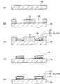
このコアレス基板の表層(図示の例では上側)には、保護膜として機能する絶縁層(ソルダレジスト層)16が、最外層の配線層(図示の例では配線層15)の所定の箇所に画定されたパッド15Pを除いて表面を覆うように形成されている。また、この絶縁層16が形成されている側と反対側(図示の例では下側)の面には、本発明を特徴付けるパッド11P(配線層11の所定の箇所に画定された部分)が露出しており、このパッド11Pは、その下面が絶縁層(樹脂層)12の下面と同一面となるように形成されている。
On the surface layer (upper side in the illustrated example) of the coreless substrate, an insulating layer (solder resist layer) 16 functioning as a protective film is defined at a predetermined position of the outermost wiring layer (the
パッド11Pは、図示のように金属層21と、金属層22と、金属層23とが順次積層された3層構造からなっている。絶縁層12から露出している側に配置される金属層21は、この露出している部分に外部接続端子もしくは半導体素子(チップ)等の電極端子が直接接合されるので、コンタクト性(はんだ付け性)の良好な材料から構成されるのが望ましい。例えば、金(Au)、金/パラジウム(Au/Pd)、錫(Sn)等を用いることができる。金属層21としてAu/Pdの2層構造を用いる場合には、Au層が配線基板10の外部に露出するよう、Au層とPd層を積層した構造とする。この金属層21の側面は、絶縁層(樹脂層)12に覆われている。
The
金属層22は、金属層21と金属層23の間に介在することで、ビア(ビアホールVH1に充填された導体)に含まれる金属(典型的には、銅(Cu))が金属層21に拡散するのを防止する役割を果たす。このような機能を実現するための材料としては、例えば、ニッケル(Ni)を用いることができる。この金属層22の側面は、絶縁層(樹脂層)12に覆われている。
By interposing the
金属層23は、この部分にビア(Cu)が直接接続されるので、良好な導電性を有し、かつ、その下層の金属層22よりも酸化され難い材料から構成されるのが望ましい。例えば、銅(Cu)、銀(Ag)、金(Au)等を用いることができる。この金属層23の側面及び上面の一部は、絶縁層(樹脂層)12に覆われている。このように金属層23は、その周囲の樹脂材(絶縁層12)と接する表面積が相対的に大きいので、樹脂との密着性が良好な材料から構成されるのが望ましい。これらの条件を考慮して、本実施形態では、金属層23の材料として銅(Cu)を用いている。
Since the via (Cu) is directly connected to this portion, the
そして、本発明の所期の目的を達成するため、樹脂との密着性が良好なCu層(金属層23)の厚さを可及的に厚く形成している。Cu層(金属層23)の厚さは、好適には、後述するようにNi層(金属層22)の厚さの3倍以上に選定されている。 In order to achieve the intended purpose of the present invention, the Cu layer (metal layer 23) having good adhesion to the resin is formed as thick as possible. The thickness of the Cu layer (metal layer 23) is preferably selected to be at least three times the thickness of the Ni layer (metal layer 22) as will be described later.
さらに、パッド11Pの表面、特定的には、その厚く形成されたCu層(金属層23)の側面及び上面を粗面化し(粗化処理)、その表面を凹凸状態としている(図中、「ギザギザ」の線で表した部分)。なお、この粗化処理は、図示のように他の配線層13,15の表面(側面及び上面)に対しても施されている。
Further, the surface of the
上側の絶縁層(ソルダレジスト層)16から露出するパッド15Pには、本配線基板10に搭載される半導体素子(チップ)等の電極端子がはんだバンプ等を介してフリップチップ接続され、下側の絶縁層(樹脂層)12から露出するパッド11Pには、本配線基板10をマザーボード等に実装する際に使用されるはんだボール等の外部接続端子が接合されるようになっている。つまり、上側の面はチップ搭載面、下側の面は外部接続端子接合面となっている。
Electrode terminals such as semiconductor elements (chips) mounted on the
ただし、本配線基板10が使用される条件、状況等によっては、チップ搭載面と外部接続端子接合面を上下反対の形態としてもよい。この場合、上側のパッド15Pに外部接続端子が接合され、下側のパッド11Pに半導体素子等の電極端子が接続される。
However, the chip mounting surface and the external connection terminal bonding surface may be formed upside down depending on conditions, conditions, and the like in which the
なお、本配線基板10の片面に形成されるソルダレジスト層16は、保護膜としての機能の他に、補強層としての役割も果たす。すなわち、本配線基板10は剛性の小さいコアレス基板であってその厚さも薄いため、基板の強度が少なからず低下することは否めないが、図示のように基板の片面にソルダレジスト層16を形成することで基板の補強を図っている。
Note that the solder resist
本実施形態に係る配線基板10を構成する各部材の具体的な材料や大きさ、厚さ等については、以下に記述するプロセスに関連させて具体的に説明する。
Specific materials, sizes, thicknesses, and the like of the respective members constituting the
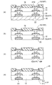
次に、本実施形態に係る配線基板10(図1)を製造する方法について、その製造工程の一例を示す図2及び図3を参照しながら説明する。 Next, a method for manufacturing the wiring board 10 (FIG. 1) according to the present embodiment will be described with reference to FIGS. 2 and 3 showing an example of the manufacturing process.
先ず最初の工程では(図2(a)参照)、仮基板としての支持基材30を用意する。この支持基材30の材料としては、後述するように最終的にはエッチングされることを考慮して、エッチング液で溶解可能な金属(典型的には、銅(Cu))が用いられる。また、支持基材30の形態としては、基本的には金属板もしくは金属箔で十分である。具体的には、例えば、プリプレグ(補強材のガラス布にエポキシ樹脂、ポリイミド樹脂等の熱硬化性樹脂を含浸させ、半硬化のBステージ状態にした接着シート)上に下地層及び銅箔を配置して加熱・加圧することにより得られた構造体(例えば、特開2007−158174号公報に開示された支持基材)を、支持基材30として好適に使用することができる。
First, in the first step (see FIG. 2A), a
次の工程では(図2(b)参照)、支持基材30上に、パターニング材料を使用してめっき用レジストを形成し、所定の部分を開口する。この開口する部分は、形成すべき所要の配線層(特定的にはパッド)の形状に従ってパターニング形成される。パターニング材料としては、感光性のドライフィルム又は液状のフォトレジストを用いることができる。例えば、ドライフィルムを使用する場合には、支持基材30の表面を洗浄した後、ドライフィルムを熱圧着により貼り付け、このドライフィルムを、所要の配線層の形状にパターニングされたマスク(図示せず)を用いて紫外線(UV)照射による露光を施して硬化させ、さらに所定の現像液を用いて当該部分をエッチング除去し(開口部OP)、所要の配線層(パッド11P)の形状に応じためっきレジスト層31を形成する。液状のフォトレジストを用いた場合にも、同様の工程を経て、めっきレジスト層31を形成することができる。
In the next step (see FIG. 2B), a plating resist is formed on the
次の工程では(図2(c)参照)、めっきレジスト層31の開口部OPから露出している支持基材(Cu)30上に、この支持基材30を給電層として利用した電解めっきにより、配線層11を形成する。この配線層11の一部(所定の箇所に画定された部分)は、外部接続端子(図4のはんだボール20)を接合するためのパッド11P(もしくは半導体素子(チップ)を搭載するためのパッド)として機能する。
In the next step (see FIG. 2C), electrolytic plating using the
パッド11Pの大きさ(直径)は、外部接続端子接合用として用いる場合には200〜1000μm程度に選定され、チップ搭載用として用いる場合には50〜150μm程度に選定される。また、パッド11Pは、上述したように3層の金属層21,22,23が積層された構造を有しており、その最下層の金属層21を構成する材料としては、これに接触する支持基材30が最終的にエッチングされることを考慮して、そのエッチング液で溶解されない金属種を選定する。本実施形態では、支持基材30の材料として銅(Cu)を用いているので、これとは異なる金属として、良好なコンタクト性を確保できるという点を考慮し、金(Au)を使用している。
The size (diameter) of the
具体的には、先ず支持基材(Cu)30上にAuフラッシュめっきを施して厚さ5nm以上(好適には40nm)のAu層を形成し、さらにAu層上にパラジウム(Pd)フラッシュめっきを施して厚さ5nm以上(好適には20nm)のPd層を形成して、Au/Pd層(金属層21)を形成する。次いで、このAu/Pd層(金属層21)上にニッケル(Ni)めっきを施して厚さ1〜10μm(好適には5μm)のNi層(金属層22)を形成し、さらにNi層(金属層22)上に銅(Cu)めっきを施して厚さ10〜20μm(好適には15μm)のCu層(金属層23)を形成する。ここに、金属層21の上層部分であるPd層は、その下層部分であるAu層の酸化を防止するために形成され、Ni層(金属層22)は、その上層の金属層23に含まれるCuが下層のAu/Pd層(金属層21)に拡散するのを防止するために形成されている。
Specifically, first, Au flash plating is performed on the support substrate (Cu) 30 to form an Au layer having a thickness of 5 nm or more (preferably 40 nm), and further, palladium (Pd) flash plating is formed on the Au layer. And a Pd layer having a thickness of 5 nm or more (preferably 20 nm) is formed to form an Au / Pd layer (metal layer 21). Next, nickel (Ni) plating is performed on the Au / Pd layer (metal layer 21) to form a Ni layer (metal layer 22) having a thickness of 1 to 10 μm (preferably 5 μm). Copper (Cu) plating is applied on the layer 22) to form a Cu layer (metal layer 23) having a thickness of 10 to 20 μm (preferably 15 μm). Here, the Pd layer that is the upper layer portion of the
つまり、この工程では、Au/Pd層21とNi層22とCu層23の3層(厳密には4層)構造からなるパッド11P(配線層11)を形成する。そして、樹脂との密着性が良好なCu層23の厚さを可及的に厚く、好適にはNi層22の厚さの3倍以上に形成している。
That is, in this step, the
次の工程では(図2(d)参照)、めっきレジスト層31(図2(c))として用いたドライフィルムレジストを、例えば、水酸化ナトリウムやモノエタノールアミン系などのアルカリ性の薬液を用いて除去する。 In the next step (see FIG. 2 (d)), the dry film resist used as the plating resist layer 31 (FIG. 2 (c)) is used, for example, using an alkaline chemical such as sodium hydroxide or monoethanolamine. Remove.
次の工程では(図2(e)参照)、支持基材30の上面側、特定的にはパッド11Pの表面を粗面化するための表面処理(粗化処理)を行う。粗化処理の方法としては、エッチング、酸化、ブラスト等の方法がある。本実施形態では、メック社製のCZ処理液(ギ酸と塩酸の混合液)を用いて所要の粗化処理を行っている。すなわち、CZ処理液の入った処理槽中に処理対象物(図2(d)の構造体)を浸漬し、あるいはCZ処理液を処理対象物にスプレーした後、水洗して処理液を洗い落とし、銅(Cu)表面を粗らしている。
In the next step (see FIG. 2E), a surface treatment (roughening treatment) is performed to roughen the upper surface side of the
図示の例では、パッド11Pの上層(Cu層23)の上面及び側面のみが粗化されている状態が示されているが、実際は、支持基材(Cu)30の表面も同様に粗化される。粗化処理後の銅(Cu)表面の粗度(Ra)は、0.2〜1.0μm程度である。なお、この粗化処理に際し、パッド11Pを構成する下層側のNi層22及びAu/Pd層21はその影響を受けない(つまり、その表面は粗化されない)。
In the illustrated example, only the upper surface and the side surface of the upper layer (Cu layer 23) of the
CZ処理以外の方法としては、例えば、黒色酸化処理(ブラックオキサイド)や、過硫酸アンモニア溶液のスプレーによるソフトエッチングを行ってもよい。いずれの処理も、銅(Cu)と樹脂との密着性を高めるためのものであり、基本的にはCu表面に凹凸を形成してアンカー効果をもたせるものである。 As a method other than the CZ treatment, for example, black oxidation treatment (black oxide) or soft etching by spraying with an ammonia persulfate solution may be performed. All the treatments are for improving the adhesion between copper (Cu) and the resin, and basically, an unevenness is formed on the Cu surface to provide an anchor effect.
次の工程では(図3(a)参照)、粗化処理を施したパッド11P(配線層11)及び支持基材30上に、パッド11Pが露出するように絶縁層12を形成する。具体的には、先ず全面に、エポキシ系樹脂やポリイミド系樹脂等からなる絶縁層12を形成する。例えば、エポキシ系樹脂フィルムを支持基材30及び配線層11(パッド11P)上にラミネートし、この樹脂フィルムをプレスしながら130〜150℃の温度で熱処理して硬化させることにより、絶縁層12を形成することができる。
In the next step (see FIG. 3A), the insulating
次いで、この絶縁層12の所定の箇所(パッド11Pに対応する部分)に、CO2 レーザ、エキシマレーザ等による穴明け処理により、パッド11Pに達する開口部(ビアホールVH1)を形成する。なお、絶縁層12は、感光性樹脂膜をフォトリソグラフィによりパターニングして形成してもよいし、あるいは、スクリーン印刷により開口部が設けられた樹脂膜をパターニングして形成してもよい。
Next, an opening (via hole VH1) reaching the
次の工程では(図3(b)参照)、ビアホールVH1が形成された絶縁層12上に、ビアホールVH1を充填して(ビアの形成)配線層11(パッド11P)に接続される所要の配線層(パターン)13を形成する。この配線層13は、例えば、セミアディティブ法により形成される。具体的には、先ず、無電解めっきやスパッタリング等により、ビアホールVH1の内部を含めて絶縁層12上に銅(Cu)のシード層(図示せず)を形成した後、形成すべき配線層13の形状に応じた開口部を備えたレジスト膜(図示せず)を形成する。次に、このレジスト膜の開口部から露出しているシード層(Cu)上に、このシード層を給電層として利用した電解銅(Cu)めっきにより、導体(Cu)パターン(図示せず)を形成する。さらに、レジスト膜を除去した後に、導体(Cu)パターンをマスクにしてシード層をエッチングすることで、所要の配線層13が得られる。なお、上記のセミアディティブ法以外に、サブトラクティブ法など各種の配線形成方法を用いることも可能である。
In the next step (see FIG. 3B), the required wiring connected to the wiring layer 11 (
このようにして所要の配線層13を形成した後、図2(e)の工程で行った処理と同様にして、配線層13の表面(側面及び上面)に粗化処理を施す。
After the required
次の工程では(図3(c)参照)、図3(a)及び(b)の工程で行った処理と同様にして、絶縁層と配線層を交互に積層する。図示の例では、簡単化のため、1層の絶縁層と1層の配線層が積層されている。すなわち、絶縁層(樹脂層)12及び配線層13上に絶縁層(樹脂層)14を形成し、この絶縁層14に、配線層13のパッド(図示せず)に達するビアホールVH2を形成した後、このビアホールVH2の内部を含めて絶縁層14上に所要の配線層(パターン)15を形成する。この配線層15は、本実施形態では最外層の配線層を構成する。
In the next step (see FIG. 3C), insulating layers and wiring layers are alternately laminated in the same manner as the processing performed in the steps of FIGS. 3A and 3B. In the illustrated example, one insulating layer and one wiring layer are stacked for simplification. That is, after an insulating layer (resin layer) 14 is formed on the insulating layer (resin layer) 12 and the
さらに、この最外層の配線層15の所定の箇所に画定されるパッド15Pを除いてその表面(絶縁層14及び配線層15)を覆うようにソルダレジスト層16を形成する。このソルダレジスト層16は、図2(b)の工程で行った処理と同様の手法を用いて形成することができる。すなわち、感光性のドライフィルムレジストをラミネートし、又は液状のフォトレジストを塗布し、当該レジストを所要の形状にパターニングすることでソルダレジスト層16を形成することができる。これによって、ソルダレジスト層16の開口部からパッド15Pが露出する。
Further, a solder resist
このパッド15Pには、搭載される半導体素子等の電極端子や、マザーボード等に実装する際に使用されるはんだボールやピン等の外部接続端子が接合されるので、コンタクト性を良くするためにAuめっきを施しておくのが望ましい。その際、パッド(Cu)15P上に無電解Niめっきを施してから無電解Auめっきを施す。つまり、Ni層とAu層の2層構造からなる導体層(図示せず)をパッド15P上に形成しておく。
The
最後の工程では(図3(d)参照)、仮基板として用いた支持基材30(図3(c))を、パッド11P、樹脂層12、パッド15P及びソルダレジスト層16に対して選択的に除去する。例えば、塩化第二鉄水溶液、塩化第二銅水溶液、過硫酸アンモニウム水溶液等を用いたウェットエッチングにより、パッド11P(その表層部にAu/Pd層21が形成されている)、樹脂層12、パッド15P(その表層部にAu層が形成されている)及びソルダレジスト層16に対して、支持基材(Cu)30を選択的にエッチングして除去することができる。
In the last step (see FIG. 3D), the supporting base material 30 (FIG. 3C) used as the temporary substrate is selectively used with respect to the
以上の工程により、本実施形態の配線基板10(図1)が製造されたことになる。 The wiring board 10 (FIG. 1) of this embodiment is manufactured by the above process.
以上説明したように、第1の実施形態に係る配線基板(半導体パッケージ)10及びその製造方法(図1〜図3)によれば、先ず、パッド11PをAu/Pd層(金属層21)とNi層(金属層22)とCu層(金属層23)との3層構造とし、Ni層22よりも酸化され難いCu層23をNi層22とビア(ビアホールVH1に充填された導体で、配線層13を構成する材料(Cu)の一部分からなるもの)との間に介在させているので、パッド11Pとビアとの間に酸化物が介在する可能性は実質的に無くなり、これにより、パッド11Pとビアとの密着性を向上させることができる。
As described above, according to the wiring substrate (semiconductor package) 10 and the manufacturing method (FIGS. 1 to 3) according to the first embodiment, first, the
さらに本実施形態では、樹脂との密着性が良好なCu層(金属層23)の厚さを可及的に厚く形成しているので、パッド11P(特定的にはCu層23)の壁面において周囲の樹脂層(絶縁層12)と接する表面積が大きくなり、樹脂層との密着性が増大する。これにより、このパッド11Pに外部接続端子(はんだボールやピン等)や半導体素子の電極端子等を接合したときの引っ張り強度が高められ、パッドが剥離するといった不良モードを大いに減らすことができる。このことは、配線基板10の性能向上につながり、ひいては、配線基板10に半導体素子等を搭載もしくは配線基板10をマザーボード等に実装する際の信頼性の向上に寄与する。
Furthermore, in this embodiment, since the thickness of the Cu layer (metal layer 23) having good adhesion to the resin is formed as thick as possible, on the wall surface of the
さらに本実施形態では、パッド11Pの表面(特定的にはCu層23の側面及び上面)に粗化処理が施されているので、パッド11Pの周囲の樹脂層(絶縁層12)との密着性を効果的に高めることができる。
Furthermore, in this embodiment, since the roughening process is performed on the surface of the
また、配線基板10の片面がソルダレジスト層16で覆われていることにより基板全体が補強されているので、基板全体の反りが抑制されて、実装時の取扱い性が向上する。
In addition, since the entire substrate is reinforced by covering one surface of the
図4は、発明技術の配線基板(特定的には図1の配線基板10)によって得られる「引っ張り強度の改善」の効果を示したものである。図中、(a)は配線基板10におけるパッド11Pの近傍部分の拡大図であり、図示の例では、このパッド11Pに外部接続端子としてのはんだボール20を接合した状態を示している。パッド11Pの最下層を構成するAu/Pd層21(図1)については、その厚さが他のNi層22、Cu層23と比べて極めて薄いため、その図示を省略している。また、(b)はパッドの厚さ(μm)を変えたときの当該パッド厚に対する引っ張り強度(gf)の変化の様子を示している。
FIG. 4 shows the effect of “improvement of tensile strength” obtained by the wiring board of the inventive technique (specifically, the
図4(b)の実験結果に示すように、樹脂層12との密着度(引っ張り強度)は、Ni層(5μm)上に形成されるCu層の厚さが厚くなるに従って増大し、特に、Cu層の厚さが12〜13μm(Ni層とCu層の厚さの合計が17〜18μm)程度になった時点で引っ張り強度が顕著に増大している。ちなみに、現状の技術では、Ni層とCu層の厚さの合計は高々14〜15μm程度であり、そのときの引っ張り強度は150gf程度であるが、本実施形態では、Cu層の厚さを15μm以上(Ni層とCu層の厚さの合計を20μm以上)に選定しているので、引っ張り強度を220gf以上に改善することができる。図示の例からわかるように、Ni層とCu層の厚さの合計は、20〜30μm程度あれば、実用上、十分な密着性を得ることができる。
As shown in the experimental results of FIG. 4B, the degree of adhesion (tensile strength) with the
(第2の実施形態…図5〜図7参照)
図5は本発明の第2の実施形態に係る配線基板(半導体パッケージ)の構成を断面図の形態で示したものである。
(Second Embodiment: See FIGS. 5 to 7)
FIG. 5 shows a configuration of a wiring board (semiconductor package) according to the second embodiment of the present invention in the form of a sectional view.
本実施形態に係る配線基板40は、第1の実施形態に係る配線基板10(図1)の構成と比べて、下側の絶縁層(樹脂層)12から露出しているパッド41Pの下面が、当該絶縁層(樹脂層)12の下面から基板内に後退した位置となるように形成されている点、このパッド41Pが、OSP(Organic Solderbility Preservative) 処理に基づいて形成される水溶性プリフラックスによる被膜(OSP膜51)と、金属層52とが積層された2層構造からなっている点で相違している。この構成では、OSP膜51は、第1の実施形態に係るパッド11PのAu/Pd層21に相当し、金属層52は、パッド11PのCu層23に相当する。つまり、本実施形態の2層構造は、従来の2層(Au/Ni)構造とは異なり、酸化され易い材料(Ni)を含んでいない。他の構成については、第1の実施形態の配線基板10と同様であるのでその説明は省略する。
The
本実施形態に係る配線基板40は、一例として図6及び図7に示す製造方法により製造することができる。図6、図7の各工程で行う処理は、基本的には、第1の実施形態に係る製造方法の各工程(図2、図3)で行った処理と同様である。重複的な説明を避けるため、相違する処理についてのみ説明する。
The
先ず、図2(a)及び(b)の工程で行った処理と同様にして、仮基板としての支持基材30を用意し(図6(a))、この支持基材30上に、所定の部分に開口部OPを備えためっきレジスト層31を形成する(図6(b))。
First, in the same manner as the processing performed in the steps of FIGS. 2A and 2B, a
次の工程では(図6(c)参照)、めっきレジスト層31の開口部OPから露出している支持基材(Cu)30上に、この支持基材30を給電層として利用した電解めっきにより、金属層22(本実施形態では、犠牲導体層として機能する)を形成し、さらにこの金属層22上に、配線層41の一部から構成されるパッド41Pの上層部分(金属層52)を形成する。パッド41Pの大きさ(直径)は、第1の実施形態の場合と同様に、外部接続端子接合用として用いる場合には200〜1000μm程度に選定され、チップ搭載用として用いる場合には50〜150μm程度に選定される。
In the next step (see FIG. 6C), electrolytic plating using the
具体的には、先ず支持基材(Cu)30上にニッケル(Ni)めっきを施して厚さ1〜10μm(好適には5μm)のNi層(金属層22)を形成し、さらにこのNi層(金属層22)上に銅(Cu)めっきを施して厚さ10〜20μm(好適には15μm)のCu層(金属層52)を形成する。このCu層52は、第1の実施形態の場合におけるCu層23(図2(c))と同様に、可及的に厚く形成され、好適にはNi層22の厚さの3倍以上に形成される。なお、この工程で形成したNi層22は、第1の実施形態の場合とは異なり、最終的にエッチングされる。
Specifically, first, nickel (Ni) plating is performed on the support base (Cu) 30 to form a Ni layer (metal layer 22) having a thickness of 1 to 10 μm (preferably 5 μm). Copper (Cu) plating is performed on the (metal layer 22) to form a Cu layer (metal layer 52) having a thickness of 10 to 20 μm (preferably 15 μm). This
次いで、図6(d)、図6(e)、図7(a)及び図7(b)の各工程において、それぞれ図2(d)、図2(e)、図3(a)〜(c)及び図3(d)の工程で行った処理と同様の処理を行う。 Next, in each step of FIG. 6D, FIG. 6E, FIG. 7A, and FIG. 7B, FIG. 2D, FIG. 2E, and FIG. c) The same processing as that performed in the step of FIG. 3D is performed.
次の工程では(図7(c)参照)、図3(d)の工程で行った処理と同様の手法を用いて、下側の樹脂層12から露出しているNi層22(図7(b))を、Cu層52、樹脂層12、パッド15P及びソルダレジスト層16に対して選択的に除去する。これによって、図示のように除去したNi層22の厚さに応じた凹部DPが形成され、この凹部DPにパッド41Pの上層部分であるCu層52の下面が露出する。
In the next step (see FIG. 7C), the
最後の工程では(図7(d)参照)、その露出されたCu層52(パッド41Pの上層部分)上にOSP処理を施して、水溶性プリフラックスによる被膜(OSP膜51)を形成する。このOSP膜51の形成により、パッド41Pに対する高いはんだ付け性を維持することができる。これによって、図示のように下側の絶縁層(樹脂層)12から露出しているパッド41Pの下面(パッド41Pの下層部分であるOSP膜51の下面)は、当該絶縁層12の下面から基板内に後退した位置となる。
In the last step (see FIG. 7D), the exposed Cu layer 52 (the upper layer portion of the
以上の工程により、本実施形態の配線基板40(図5)が製造されたことになる。 Through the above steps, the wiring board 40 (FIG. 5) of the present embodiment is manufactured.
この第2の実施形態に係る配線基板(半導体パッケージ)40及びその製造方法(図5〜図7)においても、その基本的な構成及びプロセスは第1の実施形態(図1〜図3)の場合と同じであるので、同様の作用効果を奏することができる。 Also in the wiring board (semiconductor package) 40 and its manufacturing method (FIGS. 5 to 7) according to the second embodiment, the basic configuration and process are the same as those of the first embodiment (FIGS. 1 to 3). Since it is the same as a case, the same effect can be produced.
(第3の実施形態…図8、図9参照)
図8は本発明の第3の実施形態に係る配線基板(半導体パッケージ)の構成を断面図の形態で示したものである。
(Third embodiment: see FIGS. 8 and 9)
FIG. 8 shows a configuration of a wiring board (semiconductor package) according to a third embodiment of the present invention in the form of a sectional view.
本実施形態に係る配線基板60は、第1の実施形態に係る配線基板10(図1)の構成と比べて、下側の絶縁層(樹脂層)12aから露出しているパッド11Pの下面(金属層21の下面)が、当該絶縁層(樹脂層)12aの下面から基板内に後退した位置となるように形成されている(つまり、樹脂層12aの当該部分に凹部DPが形成され、この凹部DPにパッド11Pの金属層21が露出している)点で相違している。他の構成については、第1の実施形態の配線基板10と同様であるのでその説明は省略する。
The
本実施形態に係る配線基板60は、一例として図9に示す製造方法により製造することができる。図9に示す例では、本実施形態に関連する工程のみを抜粋して示しているが、基本的には、第1の実施形態に係る製造方法(図2、図3)の場合と同様である。
The
先ず、図2(a)及び(b)の工程で行った処理と同様にして、仮基板としての支持基材30を用意し、この支持基材30上に、所定の部分に開口部OPを備えためっきレジスト層31を形成する。
First, in the same manner as the process performed in the steps of FIGS. 2A and 2B, a
この状態で、図9(a)の工程では、めっきレジスト層31の開口部OPから露出している支持基材(Cu)30上に、この支持基材30を給電層として利用した電解めっきにより、金属層24(本実施形態では、犠牲導体層として機能する)を形成し、さらにこの金属層24上に、図2(c)の工程で行った処理と同様にして、Au/Pd層21、Ni層22及びCu層23を順次積層してパッド11P(配線層11)を形成する。パッド11Pの大きさ(直径)については、第1の実施形態の場合と同じである(外部接続端子接合用:200〜1000μm程度、チップ搭載用:50〜150μm程度)。
In this state, in the process of FIG. 9A, electrolytic plating using the
この工程で形成する最下層の金属層(犠牲導体層)24を構成する材料としては、これに接触する支持基材30と共に最終的にエッチングされることを考慮して、そのエッチング液で溶解され得る金属種、この場合、銅(Cu)を選定する。また、形成すべきCu層24の厚さは、要求される凹部DP(図8)の深さに応じて決定され、例えば、10〜20μm程度の厚さに形成される。
The material constituting the lowermost metal layer (sacrificial conductor layer) 24 formed in this step is dissolved in the etching solution in consideration of the fact that it is finally etched together with the
次いで、図9(b)の工程では、図2(d)、図2(e)、図3(a)、図3(b)及び図3(c)の工程で行った処理と同様にして、めっきレジスト層31を除去し、パッド11Pの表面に粗化処理を施し、絶縁層12a(ビアホールを含む)を形成し、このビアホールを充填して配線層13を形成し、さらに絶縁層14と配線層15を交互に積層した後、ソルダレジスト層16を形成する。
Next, in the process of FIG. 9B, the process is the same as the process performed in the process of FIGS. 2D, 2E, 3A, 3B, and 3C. The plating resist
次いで、図9(c)の工程では、支持基材30(図9(b))及び犠牲導体層24を同時に除去する。すなわち、図3(d)の工程で行った処理と同様の手法(塩化第二鉄水溶液、塩化第二銅水溶液等を用いたウェットエッチング)により、パッド11P(その表層部にAu/Pd層21が形成されている)、樹脂層12a、パッド15P(その表層部にAu層が形成されている)及びソルダレジスト層16に対して、支持基材(Cu)30及び犠牲導体層(Cu)24を選択的にエッチングして除去する。これによって、図示のように除去した犠牲導体層24の厚さに応じた凹部DPが形成され、この凹部DPにパッド11Pの最下層(Au/Pd層21)が露出する。つまり、下側の樹脂層12aから露出しているパッド11Pの下面(Au/Pd層21の下面)が、当該樹脂層12aの下面から基板内に後退した位置となる。
Next, in the step of FIG. 9C, the support base material 30 (FIG. 9B) and the
以上の工程により、本実施形態の配線基板60(図8)が製造されたことになる。 The wiring board 60 (FIG. 8) of the present embodiment is manufactured through the above steps.
この第3の実施形態に係る配線基板60及びその製造方法(図9)においても、その基本的な構成及びプロセスは第1の実施形態(図1〜図3)の場合と同じであるので、同様の作用効果を奏することができる。
Also in the
上述した第1、第2、第3の各実施形態に係る配線基板10,40,60には、それぞれ使用される条件、状況等に応じて、当該基板の一方の面から露出するパッドに半導体素子(チップ)等の電極端子が接合され、他方の面から露出するパッドに外部接続端子が接合される。図10はその場合の構成例を示したものである。
In the
図10の例では、第1の実施形態に係る配線基板10に半導体素子(チップ)1を搭載した状態、すなわち、半導体装置70(70a)として構成した場合の断面構造を示している。半導体チップ1は、図中(a)に示すように配線基板10のパッド15Pが形成されている側の面に搭載してもよいし(この場合、反対側の面のパッド11Pにはんだボール20が接合される)、あるいは、図中(b)に示すように配線基板10のパッド11Pが形成されている側の面に搭載してもよい(この場合、反対側の面のパッド15Pにはんだボール20が接合される)。なお、2は半導体チップ1の電極端子、3は配線基板10と搭載した半導体チップ1との間に充填されたアンダーフィル樹脂を示す。
In the example of FIG. 10, a cross-sectional structure in a state where the semiconductor element (chip) 1 is mounted on the
図10の例では、第1の実施形態に係る配線基板10に半導体チップ1を搭載した状態を例示しているが、かかる構成に限定されることなく、第2、第3の実施形態に係る配線基板40,60についても同様に半導体チップ1を搭載できることはもちろんである。
In the example of FIG. 10, a state in which the
また、図示の例では、パッド11P(もしくは15P)にはんだボール20を接合したBGA(ボール・グリッド・アレイ)の形態としているが、当該パッドにピンを接合したPGA(ピン・グリッド・アレイ)や、当該パッド自体を外部接続端子としたLGA(ランド・グリッド・アレイ)の形態としてもよい。
Further, in the illustrated example, a BGA (ball grid array) in which
また、上述した第1、第2、第3の各実施形態では、配線基板10,40,60の形態として支持基材を含まない「コアレス基板」を使用した場合を例にとって説明したが、本発明の要旨からも明らかなように、コアレス基板に限定されないことはもちろんである。要は、パッドが複数の金属層からなり、ビアと接続される側の金属層がCu層となっている構造を有している配線基板であれば、コア基板を有した配線基板についても本発明は同様に適用することが可能である。
In the first, second, and third embodiments described above, the case where a “coreless substrate” that does not include a support base material is used as an example of the
10,40,60…配線基板(半導体パッケージ)、
11,13,15…配線層、
12,12a、14…樹脂層(絶縁層)、
11P,15P,41P…パッド、
16…ソルダレジスト層(絶縁層)、
20…はんだボール(外部接続端子)、
21,22,23,52…(パッドを構成する)金属層、
24…金属層(犠牲導体層)、
51…(パッドを構成する)OSP膜、
70,70a…半導体装置、
DP…凹部、
VH1,VH2…ビアホール。
10, 40, 60 ... wiring board (semiconductor package),
11, 13, 15 ... wiring layer,
12, 12a, 14 ... resin layer (insulating layer),
11P, 15P, 41P ... pad,
16 ... Solder resist layer (insulating layer),
20: Solder balls (external connection terminals),
21, 22, 23, 52... Metal layer (composing the pad),
24 ... Metal layer (sacrificial conductor layer),
51 ... OSP film (which constitutes a pad),
70, 70a ... semiconductor device,
DP ... recess,
VH1, VH2 ... via holes.
Claims (15)
前記パッドが、前記最外層の絶縁層からその表面が露出した第1の金属層と、該第1の金属層上に設けられ、基板内部のビアに含まれる金属が該第1の金属層に拡散するのを防止するのに有効な材料からなる第2の金属層と、該第2の金属層と前記ビアとの間に設けられ、該第2の金属層よりも酸化され難い材料からなる第3の金属層とを有し、
前記第3の金属層の厚さが他の金属層と比較して相対的に厚く選定されており、
前記第3の金属層の側面及び前記ビアとの接続面が粗面化されており、
前記第3の金属層が前記パッドの裏面となり、前記最外層の絶縁層の裏面に前記第3の金属層が露出する開口部が形成されており、前記開口部内に前記第3の金属層と接続されるビアが設けられており、前記最外層の絶縁層の裏面に前記ビアを介して前記パッドに接続される配線層が設けられていることを特徴とする配線基板。 Pads are embedded in the outermost insulating layer, the surface is exposed to the pad from the surface of the outermost insulating layers, and includes the pad rear surface and a side surface of the pad in contact with the insulating layer of the outermost layer A wiring board,
The pad is provided on the first metal layer, the surface of which is exposed from the outermost insulating layer, and the metal contained in the via inside the substrate is formed on the first metal layer. A second metal layer made of a material effective for preventing diffusion and a material that is provided between the second metal layer and the via and is less likely to be oxidized than the second metal layer. A third metal layer,
The thickness of the third metal layer is selected to be relatively thick compared to the other metal layers;
The side surface of the third metal layer and the connection surface with the via are roughened,
The third metal layer serves as a back surface of the pad, and an opening is formed in the back surface of the outermost insulating layer, and the third metal layer is exposed in the opening. A wiring board , wherein a via to be connected is provided, and a wiring layer to be connected to the pad through the via is provided on a back surface of the outermost insulating layer .
前記第2の金属層は、ニッケル層から形成され、The second metal layer is formed of a nickel layer;
前記第3の金属層は、銅層、銀層、及び金層のいずれかであることを特徴とする請求項1乃至4のいずれか一項に記載の配線基板。The wiring board according to any one of claims 1 to 4, wherein the third metal layer is any one of a copper layer, a silver layer, and a gold layer.
前記パッドの第3の金属層の表面及び側面に粗化処理を施す工程と、
前記パッドを被覆するように、前記支持基材上に樹脂からなる絶縁層を形成する工程と、
前記絶縁層に、前記第3の金属層を露出させる開口部を形成する工程と、
前記絶縁層上に、前記開口部内に設けられたビアにより前記第3の金属層に接続される配線層を形成する工程と、
前記支持基材を除去する工程とを含むことを特徴とする配線基板の製造方法。 On the support substrate, by plating, a first metal layer, and a second metal layer made of a material effective to prevent the metal contained in the via from diffusing into the first metal layer, Forming a pad by stacking a third metal layer that is made of a material that is less susceptible to oxidation than the second metal layer and is relatively thick compared to the other metal layers;
Roughening the surface and side surfaces of the third metal layer of the pad;
Forming an insulating layer made of a resin on the support base so as to cover the pad ;
Forming an opening in the insulating layer to expose the third metal layer;
Forming a wiring layer connected to the third metal layer on the insulating layer by a via provided in the opening ;
And a step of removing the supporting base material.
前記支持基材を除去する工程は、前記犠牲導体層を除去することを含むことを特徴とする請求項9に記載の配線基板の製造方法。 In the step of forming the pad, a sacrificial conductor layer is formed on the support base material by a plating method, and the pad is formed on the sacrificial conductor layer.
The method for manufacturing a wiring board according to claim 9 , wherein the step of removing the support base includes removing the sacrificial conductor layer .
前記開口部の内面を含む前記絶縁層の表面にシード層を形成し、前記シード層を給電層とする電解めっきにより、前記開口部を充填する前記ビアを形成すると共に、前記絶縁層の上に前記ビアと一体的に形成される前記配線層を形成することを含むことを特徴とする請求項9又は10に記載の配線基板の製造方法。A seed layer is formed on a surface of the insulating layer including an inner surface of the opening, and the via filling the opening is formed by electrolytic plating using the seed layer as a power feeding layer, and on the insulating layer The method for manufacturing a wiring board according to claim 9, comprising forming the wiring layer integrally formed with the via.
前記第2の金属層は、ニッケル層から形成され、The second metal layer is formed of a nickel layer;
前記第3の金属層は、銅層、銀層、及び金層のいずれかであることを特徴とする請求項9乃至11のいずれか一項に記載の配線基板の製造方法。12. The method for manufacturing a wiring board according to claim 9, wherein the third metal layer is any one of a copper layer, a silver layer, and a gold layer.
Priority Applications (4)
| Application Number | Priority Date | Filing Date | Title |
|---|---|---|---|
| JP2008234621A JP5203108B2 (en) | 2008-09-12 | 2008-09-12 | Wiring board and manufacturing method thereof |
| US12/557,847 US8399779B2 (en) | 2008-09-12 | 2009-09-11 | Wiring board and method of manufacturing the same |
| US13/764,931 US20130153271A1 (en) | 2008-09-12 | 2013-02-12 | Wiring board and method of manufacturing the same |
| US13/764,938 US9024207B2 (en) | 2008-09-12 | 2013-02-12 | Method of manufacturing a wiring board having pads highly resistant to peeling |
Applications Claiming Priority (1)
| Application Number | Priority Date | Filing Date | Title |
|---|---|---|---|
| JP2008234621A JP5203108B2 (en) | 2008-09-12 | 2008-09-12 | Wiring board and manufacturing method thereof |
Related Child Applications (1)
| Application Number | Title | Priority Date | Filing Date |
|---|---|---|---|
| JP2012184119A Division JP5580374B2 (en) | 2012-08-23 | 2012-08-23 | Wiring board and manufacturing method thereof |
Publications (3)
| Publication Number | Publication Date |
|---|---|
| JP2010067887A JP2010067887A (en) | 2010-03-25 |
| JP2010067887A5 JP2010067887A5 (en) | 2011-09-22 |
| JP5203108B2 true JP5203108B2 (en) | 2013-06-05 |
Family
ID=42006220
Family Applications (1)
| Application Number | Title | Priority Date | Filing Date |
|---|---|---|---|
| JP2008234621A Active JP5203108B2 (en) | 2008-09-12 | 2008-09-12 | Wiring board and manufacturing method thereof |
Country Status (2)
| Country | Link |
|---|---|
| US (3) | US8399779B2 (en) |
| JP (1) | JP5203108B2 (en) |
Families Citing this family (41)
| Publication number | Priority date | Publication date | Assignee | Title |
|---|---|---|---|---|
| US8240036B2 (en) | 2008-04-30 | 2012-08-14 | Panasonic Corporation | Method of producing a circuit board |
| JP5138459B2 (en) * | 2008-05-15 | 2013-02-06 | 新光電気工業株式会社 | Wiring board manufacturing method |
| KR101070098B1 (en) * | 2009-09-15 | 2011-10-04 | 삼성전기주식회사 | Printed circuit board and fabricating method of the same |
| US9332642B2 (en) | 2009-10-30 | 2016-05-03 | Panasonic Corporation | Circuit board |
| CN102598883A (en) * | 2009-10-30 | 2012-07-18 | 松下电器产业株式会社 | Circuit board, and semiconductor device having component mounted on circuit board |
| JP5504149B2 (en) * | 2009-12-28 | 2014-05-28 | 日本特殊陶業株式会社 | Multilayer wiring board |
| JP5603600B2 (en) * | 2010-01-13 | 2014-10-08 | 新光電気工業株式会社 | WIRING BOARD, MANUFACTURING METHOD THEREOF, AND SEMICONDUCTOR PACKAGE |
| US8759209B2 (en) * | 2010-03-25 | 2014-06-24 | Stats Chippac, Ltd. | Semiconductor device and method of forming a dual UBM structure for lead free bump connections |
| US8677617B2 (en) | 2010-04-28 | 2014-03-25 | International Business Machines Corporation | Printed circuit board edge connector |
| KR101156924B1 (en) | 2010-10-12 | 2012-06-21 | 삼성전기주식회사 | Method of manufacturing printed curcuit board |
| JP2012093646A (en) * | 2010-10-28 | 2012-05-17 | Seiko Epson Corp | Electronic device and manufacturing method thereof |
| KR101718011B1 (en) * | 2010-11-01 | 2017-03-21 | 삼성전자주식회사 | Semiconductor packages and methods for the same |
| JP2013093405A (en) * | 2011-10-25 | 2013-05-16 | Ngk Spark Plug Co Ltd | Wiring board and manufacturing method of the same |
| US9165878B2 (en) * | 2013-03-14 | 2015-10-20 | United Test And Assembly Center Ltd. | Semiconductor packages and methods of packaging semiconductor devices |
| CN103367296A (en) * | 2013-07-16 | 2013-10-23 | 天津威盛电子有限公司 | Electronic substrate and method for manufacturing integrated circuit with electronic substrate |
| KR20150017938A (en) * | 2013-08-08 | 2015-02-23 | 삼성전기주식회사 | Printed circuit board and manufacturing method thereof |
| JP2015041729A (en) * | 2013-08-23 | 2015-03-02 | イビデン株式会社 | Printed wiring board |
| JP5555368B1 (en) * | 2013-12-05 | 2014-07-23 | 株式会社イースタン | Wiring board manufacturing method |
| JP2015159242A (en) * | 2014-02-25 | 2015-09-03 | 京セラ株式会社 | Wiring board, and multilayer wiring board including the same |
| KR102211741B1 (en) * | 2014-07-21 | 2021-02-03 | 삼성전기주식회사 | Printed circuit board and method of manufacturing the same |
| JP2016029682A (en) * | 2014-07-25 | 2016-03-03 | イビデン株式会社 | Printed wiring board |
| JP5795415B1 (en) * | 2014-08-29 | 2015-10-14 | 新光電気工業株式会社 | Wiring board and manufacturing method thereof |
| US10325853B2 (en) | 2014-12-03 | 2019-06-18 | Taiwan Semiconductor Manufacturing Company, Ltd. | Method of forming semiconductor packages having through package vias |
| JP2016111069A (en) | 2014-12-03 | 2016-06-20 | イビデン株式会社 | Package substrate |
| US9899248B2 (en) * | 2014-12-03 | 2018-02-20 | Taiwan Semiconductor Manufacturing Company, Ltd. | Method of forming semiconductor packages having through package vias |
| JP6996976B2 (en) * | 2014-12-16 | 2022-01-17 | アンフェノール コーポレイション | High speed interconnect for printed circuit boards |
| JP2016115823A (en) | 2014-12-16 | 2016-06-23 | イビデン株式会社 | Printed wiring board |
| JP6510884B2 (en) | 2015-05-19 | 2019-05-08 | 新光電気工業株式会社 | Wiring board, method of manufacturing the same and electronic component device |
| US9779940B2 (en) * | 2015-07-01 | 2017-10-03 | Zhuahai Advanced Chip Carriers & Electronic Substrate Solutions Technologies Co. Ltd. | Chip package |
| JP6632302B2 (en) * | 2015-10-02 | 2020-01-22 | 新光電気工業株式会社 | Wiring board and manufacturing method thereof |
| US9504148B1 (en) * | 2015-12-02 | 2016-11-22 | Honeywell Federal Manufacturing & Technologies, Llc | Rapid PCB prototyping by selective adhesion |
| DE102017115252A1 (en) * | 2017-07-07 | 2019-01-10 | Osram Opto Semiconductors Gmbh | Method for producing a layer stack and layer stack |
| US10103107B1 (en) | 2017-08-08 | 2018-10-16 | Advanced Semiconductor Engineering, Inc. | Semiconductor device and method for manufacturing the same |
| TWI719241B (en) * | 2017-08-18 | 2021-02-21 | 景碩科技股份有限公司 | Multilayer circuit board capable of doing electrical test and its manufacturing method |
| WO2019188843A1 (en) * | 2018-03-28 | 2019-10-03 | 大日本印刷株式会社 | Wiring board, and method for manufacturing wiring board |
| US11569160B2 (en) * | 2018-06-06 | 2023-01-31 | Intel Corporation | Patterning of dual metallization layers |
| CN110783728A (en) * | 2018-11-09 | 2020-02-11 | 广州方邦电子股份有限公司 | Flexible connector and manufacturing method |
| KR20220098528A (en) * | 2021-01-04 | 2022-07-12 | 삼성전기주식회사 | Printed circuit board |
| US20220312591A1 (en) * | 2021-03-26 | 2022-09-29 | Juniper Networks, Inc. | Substrate with conductive pads and conductive layers |
| CN113286439A (en) * | 2021-07-22 | 2021-08-20 | 深圳市志金电子有限公司 | Method for manufacturing electroplated circuit board with built-in lead |
| CN113873762B (en) * | 2021-09-24 | 2023-10-03 | 江门崇达电路技术有限公司 | PCB with surface treatments of nickel-gold deposition and oxidation resistance and manufacturing method thereof |
Family Cites Families (25)
| Publication number | Priority date | Publication date | Assignee | Title |
|---|---|---|---|---|
| JP3085658B2 (en) | 1997-08-28 | 2000-09-11 | 京セラ株式会社 | Wiring board and manufacturing method thereof |
| USRE41242E1 (en) * | 1997-10-17 | 2010-04-20 | Ibiden Co., Ltd. | Package substrate |
| JPH11243280A (en) | 1998-02-26 | 1999-09-07 | Ibiden Co Ltd | Multilayer printed wiring board having filled via structure |
| DE69936235T2 (en) | 1998-02-26 | 2007-09-13 | Ibiden Co., Ltd., Ogaki | Multilayer printed circuit board with filled contact holes |
| JP4321913B2 (en) * | 1999-05-24 | 2009-08-26 | イビデン株式会社 | Printed wiring board |
| JP4129665B2 (en) * | 1999-10-12 | 2008-08-06 | 日本サーキット工業株式会社 | Manufacturing method of substrate for semiconductor package |
| KR100311975B1 (en) * | 1999-12-16 | 2001-10-17 | 윤종용 | semiconductor device and method for manufacturing the same |
| JP3546961B2 (en) * | 2000-10-18 | 2004-07-28 | 日本電気株式会社 | Wiring board for mounting semiconductor device, method of manufacturing the same, and semiconductor package |
| KR100499006B1 (en) * | 2002-12-30 | 2005-07-01 | 삼성전기주식회사 | Manufacturing method for package substrate without electrolytic plating lead |
| US20050067378A1 (en) * | 2003-09-30 | 2005-03-31 | Harry Fuerhaupter | Method for micro-roughening treatment of copper and mixed-metal circuitry |
| JP4108643B2 (en) | 2004-05-12 | 2008-06-25 | 日本電気株式会社 | Wiring board and semiconductor package using the same |
| JP2006186321A (en) | 2004-12-01 | 2006-07-13 | Shinko Electric Ind Co Ltd | Manufacturing method of substrate and of electronic part packaging structure |
| TWI281840B (en) * | 2005-05-09 | 2007-05-21 | Phoenix Prec Technology Corp | Electrically connecting structure of circuit board and method for fabricating same |
| US8101868B2 (en) * | 2005-10-14 | 2012-01-24 | Ibiden Co., Ltd. | Multilayered printed circuit board and method for manufacturing the same |
| TWI295550B (en) | 2005-12-20 | 2008-04-01 | Phoenix Prec Technology Corp | Structure of circuit board and method for fabricating the same |
| US7906850B2 (en) | 2005-12-20 | 2011-03-15 | Unimicron Technology Corp. | Structure of circuit board and method for fabricating same |
| TWI279897B (en) | 2005-12-23 | 2007-04-21 | Phoenix Prec Technology Corp | Embedded semiconductor chip structure and method for fabricating the same |
| US7659193B2 (en) | 2005-12-23 | 2010-02-09 | Phoenix Precision Technology Corporation | Conductive structures for electrically conductive pads of circuit board and fabrication method thereof |
| JP2007173727A (en) * | 2005-12-26 | 2007-07-05 | Shinko Electric Ind Co Ltd | Method of manufacturing wiring board |
| JP5258045B2 (en) | 2006-06-30 | 2013-08-07 | 日本電気株式会社 | Wiring board, semiconductor device using the wiring board, and manufacturing method thereof |
| DE102006052202B3 (en) * | 2006-11-06 | 2008-02-21 | Infineon Technologies Ag | Semiconductor component has metal layer comprising coherent section, and other metal layer is arranged on coherent section of former metal layer, where latter metal layer is structured between layered regions |
| JP5214139B2 (en) | 2006-12-04 | 2013-06-19 | 新光電気工業株式会社 | Wiring board and manufacturing method thereof |
| US20080268632A1 (en) * | 2007-04-30 | 2008-10-30 | Fupo Electronics Corporation. | LED epiwafer pad manufacturing process & new construction thereof |
| JP5101169B2 (en) * | 2007-05-30 | 2012-12-19 | 新光電気工業株式会社 | Wiring board and manufacturing method thereof |
| KR100896810B1 (en) * | 2007-10-16 | 2009-05-11 | 삼성전기주식회사 | Printed circuit board and method for manufacturing the same |
-
2008
- 2008-09-12 JP JP2008234621A patent/JP5203108B2/en active Active
-
2009
- 2009-09-11 US US12/557,847 patent/US8399779B2/en active Active
-
2013
- 2013-02-12 US US13/764,931 patent/US20130153271A1/en not_active Abandoned
- 2013-02-12 US US13/764,938 patent/US9024207B2/en active Active
Also Published As
| Publication number | Publication date |
|---|---|
| US8399779B2 (en) | 2013-03-19 |
| US20130185936A1 (en) | 2013-07-25 |
| US20100065322A1 (en) | 2010-03-18 |
| US9024207B2 (en) | 2015-05-05 |
| JP2010067887A (en) | 2010-03-25 |
| US20130153271A1 (en) | 2013-06-20 |
Similar Documents
| Publication | Publication Date | Title |
|---|---|---|
| JP5203108B2 (en) | Wiring board and manufacturing method thereof | |
| JP5580374B2 (en) | Wiring board and manufacturing method thereof | |
| JP5026400B2 (en) | Wiring board and manufacturing method thereof | |
| JP5339928B2 (en) | Wiring board and manufacturing method thereof | |
| US8338718B2 (en) | Wiring board and method of manufacturing the same | |
| KR101319808B1 (en) | Method of manufacturing rigid-flexible printed circuit board | |
| EP2066160B1 (en) | Wiring board and electronic component device | |
| JP4427874B2 (en) | Multilayer wiring board manufacturing method and multilayer wiring board | |
| US10892216B2 (en) | Wiring substrate and semiconductor device | |
| JP2003209366A (en) | Flexible multilayer wiring board and manufacturing method therefor | |
| JP2008300507A (en) | Wiring substrate and manufacturing process of the same | |
| JP2004193549A (en) | Package substrate plated without plated lead-in wire and its manufacturing method | |
| JP2013105908A (en) | Wiring board | |
| JP6632302B2 (en) | Wiring board and manufacturing method thereof | |
| JP5539759B2 (en) | Printed circuit board manufacturing method | |
| JP7430481B2 (en) | Wiring board, semiconductor device, and wiring board manufacturing method | |
| JP2010067888A (en) | Wiring board and method of manufacturing the same | |
| JP6691031B2 (en) | Wiring board, manufacturing method thereof, and semiconductor package | |
| JP5315447B2 (en) | Wiring board and manufacturing method thereof | |
| JP6457881B2 (en) | Wiring board and manufacturing method thereof | |
| JP5062533B2 (en) | Wiring board manufacturing method | |
| JP2003204011A (en) | Multilayer wiring board and manufacturing method there for | |
| JP4591098B2 (en) | Manufacturing method of semiconductor device mounting substrate | |
| KR101730468B1 (en) | Printed circuit board which contains bumps and manufacturing method thereof | |
| JP2002026516A (en) | Multilayer interconnection board and its manufacturing method |
Legal Events
| Date | Code | Title | Description |
|---|---|---|---|
| A521 | Request for written amendment filed |
Free format text: JAPANESE INTERMEDIATE CODE: A523 Effective date: 20110803 |
|
| A621 | Written request for application examination |
Free format text: JAPANESE INTERMEDIATE CODE: A621 Effective date: 20110803 |
|
| A977 | Report on retrieval |
Free format text: JAPANESE INTERMEDIATE CODE: A971007 Effective date: 20120629 |
|
| A131 | Notification of reasons for refusal |
Free format text: JAPANESE INTERMEDIATE CODE: A131 Effective date: 20120703 |
|
| A521 | Request for written amendment filed |
Free format text: JAPANESE INTERMEDIATE CODE: A523 Effective date: 20120823 |
|
| TRDD | Decision of grant or rejection written | ||
| A01 | Written decision to grant a patent or to grant a registration (utility model) |
Free format text: JAPANESE INTERMEDIATE CODE: A01 Effective date: 20130205 |
|
| A61 | First payment of annual fees (during grant procedure) |
Free format text: JAPANESE INTERMEDIATE CODE: A61 Effective date: 20130213 |
|
| R150 | Certificate of patent or registration of utility model |
Ref document number: 5203108 Country of ref document: JP Free format text: JAPANESE INTERMEDIATE CODE: R150 Free format text: JAPANESE INTERMEDIATE CODE: R150 |
|
| FPAY | Renewal fee payment (event date is renewal date of database) |
Free format text: PAYMENT UNTIL: 20160222 Year of fee payment: 3 |