KR101591855B1 - Fabricating method for semiconductor integrated circuit device - Google Patents
Fabricating method for semiconductor integrated circuit device Download PDFInfo
- Publication number
- KR101591855B1 KR101591855B1 KR1020080079538A KR20080079538A KR101591855B1 KR 101591855 B1 KR101591855 B1 KR 101591855B1 KR 1020080079538 A KR1020080079538 A KR 1020080079538A KR 20080079538 A KR20080079538 A KR 20080079538A KR 101591855 B1 KR101591855 B1 KR 101591855B1
- Authority
- KR
- South Korea
- Prior art keywords
- film
- nitride film
- oxide film
- delete delete
- hydrofluoric acid
- Prior art date
Links
- 239000004065 semiconductor Substances 0.000 title claims abstract description 85
- 238000000034 method Methods 0.000 title claims description 39
- 150000004767 nitrides Chemical class 0.000 claims abstract description 146
- KRHYYFGTRYWZRS-UHFFFAOYSA-N Fluorane Chemical compound F KRHYYFGTRYWZRS-UHFFFAOYSA-N 0.000 claims abstract description 142
- 239000000758 substrate Substances 0.000 claims abstract description 57
- -1 spacer nitride Chemical class 0.000 claims description 42
- 238000005530 etching Methods 0.000 claims description 25
- 230000000903 blocking effect Effects 0.000 claims description 24
- 239000012535 impurity Substances 0.000 claims description 24
- 125000006850 spacer group Chemical group 0.000 claims description 21
- 229910021332 silicide Inorganic materials 0.000 claims description 14
- FVBUAEGBCNSCDD-UHFFFAOYSA-N silicide(4-) Chemical compound [Si-4] FVBUAEGBCNSCDD-UHFFFAOYSA-N 0.000 claims description 14
- 239000000853 adhesive Substances 0.000 claims description 12
- 230000001070 adhesive effect Effects 0.000 claims description 12
- 238000001039 wet etching Methods 0.000 claims 1
- 238000004519 manufacturing process Methods 0.000 abstract description 23
- NBIIXXVUZAFLBC-UHFFFAOYSA-N Phosphoric acid Chemical compound OP(O)(O)=O NBIIXXVUZAFLBC-UHFFFAOYSA-N 0.000 description 22
- 229910000147 aluminium phosphate Inorganic materials 0.000 description 11
- 238000005229 chemical vapour deposition Methods 0.000 description 5
- XUIMIQQOPSSXEZ-UHFFFAOYSA-N Silicon Chemical compound [Si] XUIMIQQOPSSXEZ-UHFFFAOYSA-N 0.000 description 4
- 238000005224 laser annealing Methods 0.000 description 4
- 238000004518 low pressure chemical vapour deposition Methods 0.000 description 4
- 230000003647 oxidation Effects 0.000 description 4
- 238000007254 oxidation reaction Methods 0.000 description 4
- 238000001020 plasma etching Methods 0.000 description 4
- 238000004151 rapid thermal annealing Methods 0.000 description 4
- 229910052710 silicon Inorganic materials 0.000 description 4
- 239000010703 silicon Substances 0.000 description 4
- 238000003860 storage Methods 0.000 description 4
- 238000010438 heat treatment Methods 0.000 description 3
- AQYSYJUIMQTRMV-UHFFFAOYSA-N hypofluorous acid Chemical compound FO AQYSYJUIMQTRMV-UHFFFAOYSA-N 0.000 description 3
- 239000000463 material Substances 0.000 description 3
- YCKRFDGAMUMZLT-UHFFFAOYSA-N Fluorine atom Chemical compound [F] YCKRFDGAMUMZLT-UHFFFAOYSA-N 0.000 description 2
- BPQQTUXANYXVAA-UHFFFAOYSA-N Orthosilicate Chemical compound [O-][Si]([O-])([O-])[O-] BPQQTUXANYXVAA-UHFFFAOYSA-N 0.000 description 2
- 229910052785 arsenic Inorganic materials 0.000 description 2
- RQNWIZPPADIBDY-UHFFFAOYSA-N arsenic atom Chemical compound [As] RQNWIZPPADIBDY-UHFFFAOYSA-N 0.000 description 2
- 238000001505 atmospheric-pressure chemical vapour deposition Methods 0.000 description 2
- 230000004888 barrier function Effects 0.000 description 2
- 230000015572 biosynthetic process Effects 0.000 description 2
- 229910052731 fluorine Inorganic materials 0.000 description 2
- 239000011737 fluorine Substances 0.000 description 2
- 238000005468 ion implantation Methods 0.000 description 2
- 150000002500 ions Chemical class 0.000 description 2
- 238000002955 isolation Methods 0.000 description 2
- 229910052751 metal Inorganic materials 0.000 description 2
- 239000002184 metal Substances 0.000 description 2
- 238000000623 plasma-assisted chemical vapour deposition Methods 0.000 description 2
- 229910021420 polycrystalline silicon Inorganic materials 0.000 description 2
- 229920005591 polysilicon Polymers 0.000 description 2
- XLYOFNOQVPJJNP-UHFFFAOYSA-N water Chemical compound O XLYOFNOQVPJJNP-UHFFFAOYSA-N 0.000 description 2
- 229910018072 Al 2 O 3 Inorganic materials 0.000 description 1
- JBRZTFJDHDCESZ-UHFFFAOYSA-N AsGa Chemical compound [As]#[Ga] JBRZTFJDHDCESZ-UHFFFAOYSA-N 0.000 description 1
- ZOXJGFHDIHLPTG-UHFFFAOYSA-N Boron Chemical compound [B] ZOXJGFHDIHLPTG-UHFFFAOYSA-N 0.000 description 1
- 229910001218 Gallium arsenide Inorganic materials 0.000 description 1
- 229920004449 Halon® Polymers 0.000 description 1
- DGAQECJNVWCQMB-PUAWFVPOSA-M Ilexoside XXIX Chemical compound C[C@@H]1CC[C@@]2(CC[C@@]3(C(=CC[C@H]4[C@]3(CC[C@@H]5[C@@]4(CC[C@@H](C5(C)C)OS(=O)(=O)[O-])C)C)[C@@H]2[C@]1(C)O)C)C(=O)O[C@H]6[C@@H]([C@H]([C@@H]([C@H](O6)CO)O)O)O.[Na+] DGAQECJNVWCQMB-PUAWFVPOSA-M 0.000 description 1
- 229910004298 SiO 2 Inorganic materials 0.000 description 1
- 229910000577 Silicon-germanium Inorganic materials 0.000 description 1
- ATJFFYVFTNAWJD-UHFFFAOYSA-N Tin Chemical compound [Sn] ATJFFYVFTNAWJD-UHFFFAOYSA-N 0.000 description 1
- LEVVHYCKPQWKOP-UHFFFAOYSA-N [Si].[Ge] Chemical compound [Si].[Ge] LEVVHYCKPQWKOP-UHFFFAOYSA-N 0.000 description 1
- 238000007792 addition Methods 0.000 description 1
- 229910052796 boron Inorganic materials 0.000 description 1
- 239000000919 ceramic Substances 0.000 description 1
- 230000006835 compression Effects 0.000 description 1
- 238000007906 compression Methods 0.000 description 1
- 230000000694 effects Effects 0.000 description 1
- 229910052735 hafnium Inorganic materials 0.000 description 1
- VBJZVLUMGGDVMO-UHFFFAOYSA-N hafnium atom Chemical compound [Hf] VBJZVLUMGGDVMO-UHFFFAOYSA-N 0.000 description 1
- CUPFNGOKRMWUOO-UHFFFAOYSA-N hydron;difluoride Chemical compound F.F CUPFNGOKRMWUOO-UHFFFAOYSA-N 0.000 description 1
- 239000012212 insulator Substances 0.000 description 1
- 230000000873 masking effect Effects 0.000 description 1
- 229920002120 photoresistant polymer Polymers 0.000 description 1
- 238000002360 preparation method Methods 0.000 description 1
- 239000010453 quartz Substances 0.000 description 1
- 238000004904 shortening Methods 0.000 description 1
- 239000005368 silicate glass Substances 0.000 description 1
- VYPSYNLAJGMNEJ-UHFFFAOYSA-N silicon dioxide Inorganic materials O=[Si]=O VYPSYNLAJGMNEJ-UHFFFAOYSA-N 0.000 description 1
- 229910052814 silicon oxide Inorganic materials 0.000 description 1
- 229910052708 sodium Inorganic materials 0.000 description 1
- 239000011734 sodium Substances 0.000 description 1
- 229910021642 ultra pure water Inorganic materials 0.000 description 1
- 239000012498 ultrapure water Substances 0.000 description 1
- GFQYVLUOOAAOGM-UHFFFAOYSA-N zirconium(iv) silicate Chemical compound [Zr+4].[O-][Si]([O-])([O-])[O-] GFQYVLUOOAAOGM-UHFFFAOYSA-N 0.000 description 1
Images


Classifications
-
- H—ELECTRICITY
- H01—ELECTRIC ELEMENTS
- H01L—SEMICONDUCTOR DEVICES NOT COVERED BY CLASS H10
- H01L21/00—Processes or apparatus adapted for the manufacture or treatment of semiconductor or solid state devices or of parts thereof
- H01L21/02—Manufacture or treatment of semiconductor devices or of parts thereof
- H01L21/04—Manufacture or treatment of semiconductor devices or of parts thereof the devices having potential barriers, e.g. a PN junction, depletion layer or carrier concentration layer
- H01L21/18—Manufacture or treatment of semiconductor devices or of parts thereof the devices having potential barriers, e.g. a PN junction, depletion layer or carrier concentration layer the devices having semiconductor bodies comprising elements of Group IV of the Periodic Table or AIIIBV compounds with or without impurities, e.g. doping materials
-
- H—ELECTRICITY
- H01—ELECTRIC ELEMENTS
- H01L—SEMICONDUCTOR DEVICES NOT COVERED BY CLASS H10
- H01L29/00—Semiconductor devices specially adapted for rectifying, amplifying, oscillating or switching and having potential barriers; Capacitors or resistors having potential barriers, e.g. a PN-junction depletion layer or carrier concentration layer; Details of semiconductor bodies or of electrodes thereof ; Multistep manufacturing processes therefor
- H01L29/66—Types of semiconductor device ; Multistep manufacturing processes therefor
- H01L29/66007—Multistep manufacturing processes
- H01L29/66075—Multistep manufacturing processes of devices having semiconductor bodies comprising group 14 or group 13/15 materials
- H01L29/66227—Multistep manufacturing processes of devices having semiconductor bodies comprising group 14 or group 13/15 materials the devices being controllable only by the electric current supplied or the electric potential applied, to an electrode which does not carry the current to be rectified, amplified or switched, e.g. three-terminal devices
- H01L29/66409—Unipolar field-effect transistors
- H01L29/66477—Unipolar field-effect transistors with an insulated gate, i.e. MISFET
- H01L29/66568—Lateral single gate silicon transistors
- H01L29/66636—Lateral single gate silicon transistors with source or drain recessed by etching or first recessed by etching and then refilled
-
- H—ELECTRICITY
- H01—ELECTRIC ELEMENTS
- H01L—SEMICONDUCTOR DEVICES NOT COVERED BY CLASS H10
- H01L21/00—Processes or apparatus adapted for the manufacture or treatment of semiconductor or solid state devices or of parts thereof
- H01L21/02—Manufacture or treatment of semiconductor devices or of parts thereof
- H01L21/04—Manufacture or treatment of semiconductor devices or of parts thereof the devices having potential barriers, e.g. a PN junction, depletion layer or carrier concentration layer
- H01L21/18—Manufacture or treatment of semiconductor devices or of parts thereof the devices having potential barriers, e.g. a PN junction, depletion layer or carrier concentration layer the devices having semiconductor bodies comprising elements of Group IV of the Periodic Table or AIIIBV compounds with or without impurities, e.g. doping materials
- H01L21/30—Treatment of semiconductor bodies using processes or apparatus not provided for in groups H01L21/20 - H01L21/26
- H01L21/302—Treatment of semiconductor bodies using processes or apparatus not provided for in groups H01L21/20 - H01L21/26 to change their surface-physical characteristics or shape, e.g. etching, polishing, cutting
- H01L21/306—Chemical or electrical treatment, e.g. electrolytic etching
- H01L21/3063—Electrolytic etching
-
- H—ELECTRICITY
- H01—ELECTRIC ELEMENTS
- H01L—SEMICONDUCTOR DEVICES NOT COVERED BY CLASS H10
- H01L21/00—Processes or apparatus adapted for the manufacture or treatment of semiconductor or solid state devices or of parts thereof
- H01L21/02—Manufacture or treatment of semiconductor devices or of parts thereof
- H01L21/04—Manufacture or treatment of semiconductor devices or of parts thereof the devices having potential barriers, e.g. a PN junction, depletion layer or carrier concentration layer
- H01L21/18—Manufacture or treatment of semiconductor devices or of parts thereof the devices having potential barriers, e.g. a PN junction, depletion layer or carrier concentration layer the devices having semiconductor bodies comprising elements of Group IV of the Periodic Table or AIIIBV compounds with or without impurities, e.g. doping materials
- H01L21/30—Treatment of semiconductor bodies using processes or apparatus not provided for in groups H01L21/20 - H01L21/26
- H01L21/31—Treatment of semiconductor bodies using processes or apparatus not provided for in groups H01L21/20 - H01L21/26 to form insulating layers thereon, e.g. for masking or by using photolithographic techniques; After treatment of these layers; Selection of materials for these layers
- H01L21/3105—After-treatment
- H01L21/311—Etching the insulating layers by chemical or physical means
- H01L21/31105—Etching inorganic layers
- H01L21/31111—Etching inorganic layers by chemical means
-
- H—ELECTRICITY
- H01—ELECTRIC ELEMENTS
- H01L—SEMICONDUCTOR DEVICES NOT COVERED BY CLASS H10
- H01L21/00—Processes or apparatus adapted for the manufacture or treatment of semiconductor or solid state devices or of parts thereof
- H01L21/70—Manufacture or treatment of devices consisting of a plurality of solid state components formed in or on a common substrate or of parts thereof; Manufacture of integrated circuit devices or of parts thereof
- H01L21/77—Manufacture or treatment of devices consisting of a plurality of solid state components or integrated circuits formed in, or on, a common substrate
- H01L21/78—Manufacture or treatment of devices consisting of a plurality of solid state components or integrated circuits formed in, or on, a common substrate with subsequent division of the substrate into plural individual devices
- H01L21/82—Manufacture or treatment of devices consisting of a plurality of solid state components or integrated circuits formed in, or on, a common substrate with subsequent division of the substrate into plural individual devices to produce devices, e.g. integrated circuits, each consisting of a plurality of components
- H01L21/822—Manufacture or treatment of devices consisting of a plurality of solid state components or integrated circuits formed in, or on, a common substrate with subsequent division of the substrate into plural individual devices to produce devices, e.g. integrated circuits, each consisting of a plurality of components the substrate being a semiconductor, using silicon technology
- H01L21/8232—Field-effect technology
- H01L21/8234—MIS technology, i.e. integration processes of field effect transistors of the conductor-insulator-semiconductor type
- H01L21/8238—Complementary field-effect transistors, e.g. CMOS
- H01L21/823807—Complementary field-effect transistors, e.g. CMOS with a particular manufacturing method of the channel structures, e.g. channel implants, halo or pocket implants, or channel materials
-
- H—ELECTRICITY
- H01—ELECTRIC ELEMENTS
- H01L—SEMICONDUCTOR DEVICES NOT COVERED BY CLASS H10
- H01L21/00—Processes or apparatus adapted for the manufacture or treatment of semiconductor or solid state devices or of parts thereof
- H01L21/70—Manufacture or treatment of devices consisting of a plurality of solid state components formed in or on a common substrate or of parts thereof; Manufacture of integrated circuit devices or of parts thereof
- H01L21/77—Manufacture or treatment of devices consisting of a plurality of solid state components or integrated circuits formed in, or on, a common substrate
- H01L21/78—Manufacture or treatment of devices consisting of a plurality of solid state components or integrated circuits formed in, or on, a common substrate with subsequent division of the substrate into plural individual devices
- H01L21/82—Manufacture or treatment of devices consisting of a plurality of solid state components or integrated circuits formed in, or on, a common substrate with subsequent division of the substrate into plural individual devices to produce devices, e.g. integrated circuits, each consisting of a plurality of components
- H01L21/822—Manufacture or treatment of devices consisting of a plurality of solid state components or integrated circuits formed in, or on, a common substrate with subsequent division of the substrate into plural individual devices to produce devices, e.g. integrated circuits, each consisting of a plurality of components the substrate being a semiconductor, using silicon technology
- H01L21/8232—Field-effect technology
- H01L21/8234—MIS technology, i.e. integration processes of field effect transistors of the conductor-insulator-semiconductor type
- H01L21/8238—Complementary field-effect transistors, e.g. CMOS
- H01L21/823864—Complementary field-effect transistors, e.g. CMOS with a particular manufacturing method of the gate sidewall spacers, e.g. double spacers, particular spacer material or shape
-
- H—ELECTRICITY
- H01—ELECTRIC ELEMENTS
- H01L—SEMICONDUCTOR DEVICES NOT COVERED BY CLASS H10
- H01L29/00—Semiconductor devices specially adapted for rectifying, amplifying, oscillating or switching and having potential barriers; Capacitors or resistors having potential barriers, e.g. a PN-junction depletion layer or carrier concentration layer; Details of semiconductor bodies or of electrodes thereof ; Multistep manufacturing processes therefor
- H01L29/66—Types of semiconductor device ; Multistep manufacturing processes therefor
- H01L29/66007—Multistep manufacturing processes
- H01L29/66075—Multistep manufacturing processes of devices having semiconductor bodies comprising group 14 or group 13/15 materials
- H01L29/66227—Multistep manufacturing processes of devices having semiconductor bodies comprising group 14 or group 13/15 materials the devices being controllable only by the electric current supplied or the electric potential applied, to an electrode which does not carry the current to be rectified, amplified or switched, e.g. three-terminal devices
- H01L29/66409—Unipolar field-effect transistors
- H01L29/66477—Unipolar field-effect transistors with an insulated gate, i.e. MISFET
- H01L29/6653—Unipolar field-effect transistors with an insulated gate, i.e. MISFET using the removal of at least part of spacer, e.g. disposable spacer
-
- H—ELECTRICITY
- H01—ELECTRIC ELEMENTS
- H01L—SEMICONDUCTOR DEVICES NOT COVERED BY CLASS H10
- H01L29/00—Semiconductor devices specially adapted for rectifying, amplifying, oscillating or switching and having potential barriers; Capacitors or resistors having potential barriers, e.g. a PN-junction depletion layer or carrier concentration layer; Details of semiconductor bodies or of electrodes thereof ; Multistep manufacturing processes therefor
- H01L29/66—Types of semiconductor device ; Multistep manufacturing processes therefor
- H01L29/66007—Multistep manufacturing processes
- H01L29/66075—Multistep manufacturing processes of devices having semiconductor bodies comprising group 14 or group 13/15 materials
- H01L29/66227—Multistep manufacturing processes of devices having semiconductor bodies comprising group 14 or group 13/15 materials the devices being controllable only by the electric current supplied or the electric potential applied, to an electrode which does not carry the current to be rectified, amplified or switched, e.g. three-terminal devices
- H01L29/66409—Unipolar field-effect transistors
- H01L29/66477—Unipolar field-effect transistors with an insulated gate, i.e. MISFET
- H01L29/6656—Unipolar field-effect transistors with an insulated gate, i.e. MISFET using multiple spacer layers, e.g. multiple sidewall spacers
-
- H—ELECTRICITY
- H01—ELECTRIC ELEMENTS
- H01L—SEMICONDUCTOR DEVICES NOT COVERED BY CLASS H10
- H01L29/00—Semiconductor devices specially adapted for rectifying, amplifying, oscillating or switching and having potential barriers; Capacitors or resistors having potential barriers, e.g. a PN-junction depletion layer or carrier concentration layer; Details of semiconductor bodies or of electrodes thereof ; Multistep manufacturing processes therefor
- H01L29/66—Types of semiconductor device ; Multistep manufacturing processes therefor
- H01L29/66007—Multistep manufacturing processes
- H01L29/66075—Multistep manufacturing processes of devices having semiconductor bodies comprising group 14 or group 13/15 materials
- H01L29/66227—Multistep manufacturing processes of devices having semiconductor bodies comprising group 14 or group 13/15 materials the devices being controllable only by the electric current supplied or the electric potential applied, to an electrode which does not carry the current to be rectified, amplified or switched, e.g. three-terminal devices
- H01L29/66409—Unipolar field-effect transistors
- H01L29/66477—Unipolar field-effect transistors with an insulated gate, i.e. MISFET
- H01L29/66568—Lateral single gate silicon transistors
- H01L29/66575—Lateral single gate silicon transistors where the source and drain or source and drain extensions are self-aligned to the sides of the gate
- H01L29/6659—Lateral single gate silicon transistors where the source and drain or source and drain extensions are self-aligned to the sides of the gate with both lightly doped source and drain extensions and source and drain self-aligned to the sides of the gate, e.g. lightly doped drain [LDD] MOSFET, double diffused drain [DDD] MOSFET
-
- H—ELECTRICITY
- H01—ELECTRIC ELEMENTS
- H01L—SEMICONDUCTOR DEVICES NOT COVERED BY CLASS H10
- H01L29/00—Semiconductor devices specially adapted for rectifying, amplifying, oscillating or switching and having potential barriers; Capacitors or resistors having potential barriers, e.g. a PN-junction depletion layer or carrier concentration layer; Details of semiconductor bodies or of electrodes thereof ; Multistep manufacturing processes therefor
- H01L29/66—Types of semiconductor device ; Multistep manufacturing processes therefor
- H01L29/68—Types of semiconductor device ; Multistep manufacturing processes therefor controllable by only the electric current supplied, or only the electric potential applied, to an electrode which does not carry the current to be rectified, amplified or switched
- H01L29/76—Unipolar devices, e.g. field effect transistors
- H01L29/772—Field effect transistors
- H01L29/78—Field effect transistors with field effect produced by an insulated gate
- H01L29/7833—Field effect transistors with field effect produced by an insulated gate with lightly doped drain or source extension, e.g. LDD MOSFET's; DDD MOSFET's
-
- H—ELECTRICITY
- H01—ELECTRIC ELEMENTS
- H01L—SEMICONDUCTOR DEVICES NOT COVERED BY CLASS H10
- H01L29/00—Semiconductor devices specially adapted for rectifying, amplifying, oscillating or switching and having potential barriers; Capacitors or resistors having potential barriers, e.g. a PN-junction depletion layer or carrier concentration layer; Details of semiconductor bodies or of electrodes thereof ; Multistep manufacturing processes therefor
- H01L29/66—Types of semiconductor device ; Multistep manufacturing processes therefor
- H01L29/68—Types of semiconductor device ; Multistep manufacturing processes therefor controllable by only the electric current supplied, or only the electric potential applied, to an electrode which does not carry the current to be rectified, amplified or switched
- H01L29/76—Unipolar devices, e.g. field effect transistors
- H01L29/772—Field effect transistors
- H01L29/78—Field effect transistors with field effect produced by an insulated gate
- H01L29/7842—Field effect transistors with field effect produced by an insulated gate means for exerting mechanical stress on the crystal lattice of the channel region, e.g. using a flexible substrate
- H01L29/7843—Field effect transistors with field effect produced by an insulated gate means for exerting mechanical stress on the crystal lattice of the channel region, e.g. using a flexible substrate the means being an applied insulating layer
-
- H—ELECTRICITY
- H01—ELECTRIC ELEMENTS
- H01L—SEMICONDUCTOR DEVICES NOT COVERED BY CLASS H10
- H01L29/00—Semiconductor devices specially adapted for rectifying, amplifying, oscillating or switching and having potential barriers; Capacitors or resistors having potential barriers, e.g. a PN-junction depletion layer or carrier concentration layer; Details of semiconductor bodies or of electrodes thereof ; Multistep manufacturing processes therefor
- H01L29/66—Types of semiconductor device ; Multistep manufacturing processes therefor
- H01L29/66007—Multistep manufacturing processes
- H01L29/66075—Multistep manufacturing processes of devices having semiconductor bodies comprising group 14 or group 13/15 materials
- H01L29/66227—Multistep manufacturing processes of devices having semiconductor bodies comprising group 14 or group 13/15 materials the devices being controllable only by the electric current supplied or the electric potential applied, to an electrode which does not carry the current to be rectified, amplified or switched, e.g. three-terminal devices
- H01L29/66409—Unipolar field-effect transistors
- H01L29/66477—Unipolar field-effect transistors with an insulated gate, i.e. MISFET
- H01L29/665—Unipolar field-effect transistors with an insulated gate, i.e. MISFET using self aligned silicidation, i.e. salicide
-
- H—ELECTRICITY
- H01—ELECTRIC ELEMENTS
- H01L—SEMICONDUCTOR DEVICES NOT COVERED BY CLASS H10
- H01L29/00—Semiconductor devices specially adapted for rectifying, amplifying, oscillating or switching and having potential barriers; Capacitors or resistors having potential barriers, e.g. a PN-junction depletion layer or carrier concentration layer; Details of semiconductor bodies or of electrodes thereof ; Multistep manufacturing processes therefor
- H01L29/66—Types of semiconductor device ; Multistep manufacturing processes therefor
- H01L29/66007—Multistep manufacturing processes
- H01L29/66075—Multistep manufacturing processes of devices having semiconductor bodies comprising group 14 or group 13/15 materials
- H01L29/66227—Multistep manufacturing processes of devices having semiconductor bodies comprising group 14 or group 13/15 materials the devices being controllable only by the electric current supplied or the electric potential applied, to an electrode which does not carry the current to be rectified, amplified or switched, e.g. three-terminal devices
- H01L29/66409—Unipolar field-effect transistors
- H01L29/66477—Unipolar field-effect transistors with an insulated gate, i.e. MISFET
- H01L29/66742—Thin film unipolar transistors
- H01L29/66772—Monocristalline silicon transistors on insulating substrates, e.g. quartz substrates
Landscapes
- Engineering & Computer Science (AREA)
- Microelectronics & Electronic Packaging (AREA)
- Power Engineering (AREA)
- Condensed Matter Physics & Semiconductors (AREA)
- General Physics & Mathematics (AREA)
- Computer Hardware Design (AREA)
- Physics & Mathematics (AREA)
- Manufacturing & Machinery (AREA)
- Ceramic Engineering (AREA)
- Chemical & Material Sciences (AREA)
- Crystallography & Structural Chemistry (AREA)
- Chemical Kinetics & Catalysis (AREA)
- General Chemical & Material Sciences (AREA)
- Inorganic Chemistry (AREA)
- Metal-Oxide And Bipolar Metal-Oxide Semiconductor Integrated Circuits (AREA)
- Insulated Gate Type Field-Effect Transistor (AREA)
- Element Separation (AREA)
- Weting (AREA)
- Thin Film Transistor (AREA)
Abstract
반도체 집적 회로 장치의 제조 방법이 제공된다. 상기 반도체 집적 회로 장치의 제조 방법은 반도체 기판과, 상기 반도체 기판 상에 게이트와, 상기 게이트 측벽에 형성된 질화막과, 상기 반도체 기판과 상기 질화막 사이와 상기 게이트와 상기 질화막 사이에 형성된 산화막과, 상기 게이트에 인접하여 상기 반도체 기판 내에 형성된 불순물 영역을 포함하는 반도체 소자를 제공하고, 산화막에 대한 질화막의 선택비가 1 초과인 불산(hydrofluoric acid)을 이용하여 상기 질화막의 적어도 일부를 식각하고, 상기 반도체 기판과 상기 게이트 상에 스트레스막을 형성하는 것을 포함한다.A method of manufacturing a semiconductor integrated circuit device is provided. A gate electrode; a nitride film formed on the sidewall of the gate; an oxide film formed between the semiconductor substrate and the nitride film, between the gate and the nitride film; Wherein at least a part of the nitride film is etched by using hydrofluoric acid having a selectivity ratio of a nitride film to an oxide film of more than 1, And forming a stress film on the gate.
반도체 집적 회로 장치, 불산, 선택비, 온도, 농도 Semiconductor integrated circuit device, hydrofluoric acid, selection ratio, temperature, concentration
Description
본 발명은 안정적인 식각이 가능한 반도체 집적 회로 장치의 제조 방법에 관한 것이다.The present invention relates to a method of manufacturing a semiconductor integrated circuit device capable of stable etching.
질화막은 물리적, 화학적으로 안정적이므로, 반도체 집적 회로 장치의 제조 과정 중에 많이 사용된다. 예를 들어, 질화막은 산화막에 비해 기계적 강도, 수증기 배리어(barrier) 특성, 나트륨 배리어 특성 등이 더 우수하다. 반면, 질화막은 식각에 의해 제거하는 것이 용이하지 않다. Since the nitride film is physically and chemically stable, it is widely used in the process of manufacturing a semiconductor integrated circuit device. For example, the nitride film is superior to the oxide film in terms of mechanical strength, water vapor barrier property, and sodium barrier property. On the other hand, it is not easy to remove the nitride film by etching.
이러한 질화막은 산화막에 대해 선택적으로 제거되어야 하는 경우가 많다. 종래에는 인산(phosphoric acid, H3PO4)을 사용하여 산화막에 대해서 선택적으로 질화막을 식각하였다. 예를 들어, 인산이 담긴 배스(bath)에 질화막과 산화막이 형성된 반도체 기판을 투입하고, 배스를 약 160~170℃의 온도로 가열함으로써 식각 공정을 진행한다. 이 때, 질화막의 식각율은 약 40~45Å/min이고, 산화막의 식각율은 약 1.2~2.0Å/min 일 수 있다. 즉, 약 160~170℃의 온도에서 산화막에 대한 질화막 의 선택비(selectivity for nitride to oxide)은 약 26~27이 된다. Such a nitride film often needs to be selectively removed with respect to an oxide film. Conventionally, a nitride film is selectively etched on an oxide film using phosphoric acid (H 3 PO 4 ). For example, a semiconductor substrate on which a nitride film and an oxide film are formed is placed in a bath containing phosphoric acid, and the etching process is performed by heating the bath to a temperature of about 160 to 170 ° C. At this time, the etching rate of the nitride film is about 40 to 45 Å / min, and the etching rate of the oxide film is about 1.2 to 2.0 Å / min. That is, the selectivity for nitride to oxide for the oxide film is about 26 to 27 at a temperature of about 160 to 170 ° C.
그런데, 인산은 점성(viscosity)이 높기 때문에, 약 2시간 정도 예열(pre-heating)을 해야 약 160~170℃에 이를 수 있다. 또한, 인산은 안정성이 떨어지기 때문에, 실제 인산을 이용한 식각 공정이 진행되기 전에 적어도 2번의 더미 사이클(dummy cycle)이 요구된다. 또한, 인산을 이용한 식각은 비용이 많이 든다.However, since phosphoric acid has a high viscosity, pre-heating is required for about 2 hours to reach 160-170 ° C. In addition, since the stability of phosphoric acid is deteriorated, at least two dummy cycles are required before the etching process using actual phosphoric acid proceeds. In addition, etching using phosphoric acid is expensive.
본 발명이 이루고자 하는 기술적 과제는, 안정적인 식각이 가능한 반도체 집적 회로 장치의 제조 방법을 제공하는 것이다.SUMMARY OF THE INVENTION The present invention provides a method of manufacturing a semiconductor integrated circuit device capable of stable etching.
본 발명의 기술적 과제들은 이상에서 언급한 기술적 과제로 제한되지 않으며, 언급되지 않은 또 다른 기술적 과제들은 아래의 기재로부터 당업자에게 명확하게 이해될 수 있을 것이다.The technical objects of the present invention are not limited to the technical matters mentioned above, and other technical subjects not mentioned can be clearly understood by those skilled in the art from the following description.
상기 기술적 과제를 달성하기 위한 본 발명의 일 태양에 따른 반도체 집적 회로 장치의 제조 방법은 반도체 기판과, 상기 반도체 기판 상에 게이트와, 상기 게이트 측벽에 형성된 질화막과, 상기 반도체 기판과 상기 질화막 사이와 상기 게이트와 상기 질화막 사이에 형성된 산화막과, 상기 게이트에 인접하여 상기 반도체 기판 내에 형성된 불순물 영역을 포함하는 반도체 소자를 제공하고, 산화막에 대한 질화막의 선택비가 1 초과인 불산(hydrofluoric acid)을 이용하여 상기 질화막의 적어도 일부를 식각하고, 상기 반도체 기판과 상기 게이트 상에 스트레스막을 형성하는 것을 포함한다.According to an aspect of the present invention, there is provided a method of manufacturing a semiconductor integrated circuit device, the method including: forming a gate on a semiconductor substrate, a nitride film formed on the gate sidewall, A semiconductor element including an oxide film formed between the gate and the nitride film, and an impurity region formed in the semiconductor substrate adjacent to the gate, wherein the nitride film is formed by hydrofluoric acid Etching at least a part of the nitride film, and forming a stress film on the semiconductor substrate and the gate.
상기 기술적 과제를 달성하기 위한 본 발명의 다른 태양에 따른 반도체 집적 회로 장치의 제조 방법은 반도체 기판과, 상기 반도체 기판 상에 형성된 게이트와, 상기 게이트의 양측벽에 순차적으로 형성된 스페이서 산화막과 스페이서 질화막과, 상기 반도체 기판과 상기 스페이서 질화막 사이와 상기 스페이서 산화막과 상기 스 페이서 질화막 사이에 형성된 접착 산화막과, 상기 스페이서 산화막에 정렬되어 형성된 제1 불순물 영역과, 상기 스페이서 질화막에 정렬되어 형성된 제2 불순물 영역을 포함하는 반도체 소자를 제공하고, 산화막에 대한 질화막의 선택비가 1 초과인 불산(hydrofluoric acid)를 이용하여 상기 스페이서 질화막의 적어도 일부를 습식 식각하고, 상기 제2 불순물 영역 내에 실리사이드막을 형성하고, 상기 반도체 기판과 상기 게이트 상에 식각 정지막과 스트레스막을 순차적으로 형성하는 것을 포함한다.According to another aspect of the present invention, there is provided a method of fabricating a semiconductor integrated circuit device including a semiconductor substrate, a gate formed on the semiconductor substrate, a spacer oxide film and a spacer nitride film sequentially formed on both sidewalls of the gate, An adhesion oxide film formed between the semiconductor substrate and the spacer nitride film, between the spacer oxide film and the spacer nitride film, a first impurity region formed by being aligned with the spacer oxide film, and a second impurity region Wherein at least a part of the spacer nitride film is wet-etched using hydrofluoric acid having a selectivity ratio of a nitride film to an oxide film of more than 1 to form a silicide film in the second impurity region, The semiconductor substrate and the gate top It comprises forming the etch stop film and the film stress in order.
상기 기술적 과제를 달성하기 위한 본 발명의 또 다른 태양에 따른 집적 회로 장치의 제조 방법은 반도체 기판 상에 형성된 제1 및 제2 반도체 소자를 제공하되, 상기 각 반도체 소자는 상기 반도체 기판 상에 게이트와, 상기 게이트에 인접하여 상기 반도체 기판 내에 형성된 불순물 영역을 포함하고, 상기 제1 및 제2 반도체 소자 상에 블로킹(blocking) 산화막 및 블로킹 질화막을 순차적으로 형성하고, 산화막에 대한 질화막의 선택비가 1초과인 불산(hydrofluoric acid)를 이용하여 상기 제1 반도체 소자 상에 형성된 블로킹 질화막을 식각하는 것은 포함한다.According to another aspect of the present invention, there is provided a method of manufacturing an integrated circuit device, the method including providing first and second semiconductor devices formed on a semiconductor substrate, And an impurity region formed in the semiconductor substrate adjacent to the gate, wherein a blocking oxide film and a blocking nitride film are sequentially formed on the first and second semiconductor elements, and the selection ratio of the nitride film to the oxide film is more than 1 Etching the blocking nitride film formed on the first semiconductor element by using hydrofluoric acid.
상기 기술적 과제를 달성하기 위한 본 발명의 또 다른 태양에 따른 집적 회로 장치의 제조 방법은 반도체 기판 상에 형성된 제1 및 제2 반도체 소자를 제공하되, 상기 각 반도체 소자는 상기 반도체 기판 상에 게이트와, 상기 게이트에 인접하여 상기 반도체 기판 내에 형성된 불순물 영역을 포함하고, 상기 제1 및 제2 반도체 소자 상에 식각 정지막 및 스트레스막을 순차적으로 형성하고, 산화막에 대한 질화막의 선택비가 1초과인 불산(hydrofluoric acid)를 이용하여 상기 제1 반도체 소자 상에 형성된 스트레스막을 제거하는 것을 포함한다.According to another aspect of the present invention, there is provided a method of manufacturing an integrated circuit device, the method including providing first and second semiconductor devices formed on a semiconductor substrate, And an impurity region formed in the semiconductor substrate adjacent to the gate, wherein an etching stopper film and a stress film are sequentially formed on the first and second semiconductor elements, and a hydrofluoric acid hydrofluoric acid) to remove the stress film formed on the first semiconductor element.
상기 기술적 과제를 달성하기 위한 본 발명의 또 다른 태양에 따른 집적 회로 장치의 제조 방법은 반도체 기판 상에 순차적으로 형성된 패드 산화막 및 패드 질화막을 형성하고, 상기 패드 질화막을 식각 마스크로 이용하여 상기 반도체 기판 내에 트렌치를 형성하고, 상기 트렌치를 따라 라이너 산화막을 컨포말하게(conformally) 형성하고, 상기 라이너 산화막 및 상기 패드 질화막을 따라 라이너 질화막을 컨포말하게 형성하고, 상기 라이너 질화막 상에 상기 트렌치가 매립되도록 매립 산화막을 형성하고, 산화막에 대한 질화막의 선택비는 약 0.7 ~ 약 1.4 인 제1 불산을 이용하여 상기 패드 질화막의 상면이 노출되도록 상기 매립 산화막의 일부와 상기 라이너 질화막의 일부를 식각하고, 상기 패드 질화막을 제거하는 것을 포함한다.According to another aspect of the present invention, there is provided a method of fabricating an integrated circuit device, comprising: forming a pad oxide film and a pad nitride film sequentially formed on a semiconductor substrate; Forming a liner oxide film conformally along the trench and forming a liner nitride film along the liner oxide film and the pad nitride film to conform the trench to the liner nitride film; Etching a part of the buried oxide film and a part of the liner nitride film to expose an upper surface of the pad nitride film using a first hydrofluoric acid having a selectivity ratio of a nitride film to an oxide film of about 0.7 to about 1.4, Removing the pad nitride film.
상기 기술적 과제를 달성하기 위한 본 발명의 또 다른 태양에 따른 집적 회로 장치의 제조 방법은 반도체 기판 상에 순차적으로 형성된 패드 산화막 및 패드 질화막과, 상기 패드 산화막 및 패드 질화막을 식각 마스크로 이용하여 상기 반도체 기판 내에 형성된 트렌치와, 상기 트렌치를 따라 컨포말하게 형성된 라이너 산화막과, 상기 라이너 산화막 및 상기 패드 질화막을 따라 컨포말하게 형성된 라이너 질화막과, 상기 라이너 질화막 상에 상기 트렌치가 매립되도록 형성된 매립 산화막을 포함하는 반도체 기판을 배스(bath)에 위치시키고, 상기 배스 내에서 불산의 온도 및/또는 농도를 변화시켜가면서, 상기 매립 산화막의 일부, 상기 라이너 질화막의 일부, 상기 패드 질화막을 식각하는 것을 포함한다.According to another aspect of the present invention, there is provided a method of fabricating an integrated circuit device, comprising: forming a pad oxide film and a pad nitride film sequentially formed on a semiconductor substrate; A liner nitride film formed in conformity with the liner oxide film and the pad nitride film; and a buried oxide film formed on the liner nitride film so that the trench is buried in the liner nitride film. Etching a portion of the buried oxide layer, a portion of the liner nitride layer, and the pad nitride layer while the semiconductor substrate is placed in a bath and the temperature and / or concentration of the hydrofluoric acid is changed in the bath.
본 발명의 기타 구체적인 사항들은 상세한 설명 및 도면들에 포함되어 있다.Other specific details of the invention are included in the detailed description and drawings.
본 발명의 이점 및 특징, 그리고 그것들을 달성하는 방법은 첨부되는 도면과 함께 상세하게 후술되어 있는 실시예들을 참조하면 명확해질 것이다. 그러나 본 발명은 이하에서 개시되는 실시예들에 한정되는 것이 아니라 서로 다른 다양한 형태로 구현될 것이며, 단지 본 실시예들은 본 발명의 개시가 완전하도록 하며, 본 발명이 속하는 기술분야에서 통상의 지식을 가진 자에게 발명의 범주를 완전하게 알려주기 위해 제공되는 것이며, 본 발명은 청구항의 범주에 의해 정의될 뿐이다. 명세서 전체에 걸쳐 동일 참조 부호는 동일 구성 요소를 지칭한다.BRIEF DESCRIPTION OF THE DRAWINGS The advantages and features of the present invention, and the manner of achieving them, will be apparent from and elucidated with reference to the embodiments described hereinafter in conjunction with the accompanying drawings. The present invention may, however, be embodied in many different forms and should not be construed as being limited to the embodiments set forth herein. Rather, these embodiments are provided so that this disclosure will be thorough and complete, and will fully convey the scope of the invention to those skilled in the art. Is provided to fully convey the scope of the invention to those skilled in the art, and the invention is only defined by the scope of the claims. Like reference numerals refer to like elements throughout the specification.
하나의 소자(elements)가 다른 소자와 "접속된(connected to)" 또는 "커플링된(coupled to)" 이라고 지칭되는 것은, 다른 소자와 직접 연결 또는 커플링된 경우 또는 중간에 다른 소자를 개재한 경우를 모두 포함한다. 반면, 하나의 소자가 다른 소자와 "직접 접속된(directly connected to)" 또는 "직접 커플링된(directly coupled to)"으로 지칭되는 것은 중간에 다른 소자를 개재하지 않은 것을 나타낸다. 명세서 전체에 걸쳐 동일 참조 부호는 동일 구성 요소를 지칭한다. "및/또는"은 언급된 아이템들의 각각 및 하나 이상의 모든 조합을 포함한다. One element is referred to as being "connected to " or" coupled to "another element, either directly connected or coupled to another element, One case. On the other hand, when one element is referred to as being "directly connected to" or "directly coupled to " another element, it does not intervene another element in the middle. Like reference numerals refer to like elements throughout the specification. "And / or" include each and every combination of one or more of the mentioned items.
비록 제1, 제2 등이 다양한 소자, 구성요소 및/또는 섹션들을 서술하기 위해서 사용되나, 이들 소자, 구성요소 및/또는 섹션들은 이들 용어에 의해 제한되지 않음은 물론이다. 이들 용어들은 단지 하나의 소자, 구성요소 또는 섹션들을 다른 소자, 구성요소 또는 섹션들과 구별하기 위하여 사용하는 것이다. 따라서, 이하에 서 언급되는 제1 소자, 제1 구성요소 또는 제1 섹션은 본 발명의 기술적 사상 내에서 제2 소자, 제2 구성요소 또는 제2 섹션일 수도 있음은 물론이다.Although the first, second, etc. are used to describe various elements, components and / or sections, it is needless to say that these elements, components and / or sections are not limited by these terms. These terms are only used to distinguish one element, element or section from another element, element or section. Therefore, it goes without saying that the first element, the first element or the first section mentioned below may be the second element, the second element or the second section within the technical spirit of the present invention.
본 명세서에서 사용된 용어는 실시예들을 설명하기 위한 것이며 본 발명을 제한하고자 하는 것은 아니다. 본 명세서에서, 단수형은 문구에서 특별히 언급하지 않는 한 복수형도 포함한다. 명세서에서 사용되는 "포함한다(comprises)" 및/또는 "포함하는(comprising)"은 언급된 구성요소, 단계, 동작 및/또는 소자는 하나 이상의 다른 구성요소, 단계, 동작 및/또는 소자의 존재 또는 추가를 배제하지 않는다.The terminology used herein is for the purpose of illustrating embodiments and is not intended to be limiting of the present invention. In the present specification, the singular form includes plural forms unless otherwise specified in the specification. It is noted that the terms "comprises" and / or "comprising" used in the specification are intended to be inclusive in a manner similar to the components, steps, operations, and / Or additions.
다른 정의가 없다면, 본 명세서에서 사용되는 모든 용어(기술 및 과학적 용어를 포함)는 본 발명이 속하는 기술분야에서 통상의 지식을 가진 자에게 공통적으로 이해될 수 있는 의미로 사용될 수 있을 것이다. 또 일반적으로 사용되는 사전에 정의되어 있는 용어들은 명백하게 특별히 정의되어 있지 않는 한 이상적으로 또는 과도하게 해석되지 않는다. Unless defined otherwise, all terms (including technical and scientific terms) used herein may be used in a sense commonly understood by one of ordinary skill in the art to which this invention belongs. Also, commonly used predefined terms are not ideally or excessively interpreted unless explicitly defined otherwise.
공간적으로 상대적인 용어인 "아래(below)", "아래(beneath)", "하부(lower)", "위(above)", "상(upper)" 등은 도면에 도시되어 있는 바와 같이 하나의 소자 또는 구성 요소들과 다른 소자 또는 구성 요소들과의 상관관계를 용이하게 기술하기 위해 사용될 수 있다. 공간적으로 상대적인 용어는 도면에 도시되어 있는 방향에 더하여 사용시 또는 동작시 소자의 서로 다른 방향을 포함하는 용어로 이해되어야 한다. 예를 들면, 도면에 도시되어 있는 소자를 뒤집을 경우, 다른 소자의 "아래(below)" 또는 "아래(beneath)"로 기술된 소자는 다른 소자의 "위(above)"에 놓여질 수 있다. 따라서, 예시적인 용어인 "아래"는 아래와 위의 방향을 모두 포함 할 수 있다. 소자는 다른 방향으로도 배향될 수 있고, 이에 따라 공간적으로 상대적인 용어들은 배향에 따라 해석될 수 있다. The terms spatially relative, "below", "beneath", "lower", "above", "upper" May be used to readily describe a device or a relationship of components to other devices or components. Spatially relative terms should be understood to include, in addition to the orientation shown in the drawings, terms that include different orientations of the device during use or operation. For example, when inverting an element shown in the figures, an element described as "below" or "beneath" of another element may be placed "above" another element. Thus, the exemplary term "below" can include both downward and upward directions. The elements can also be oriented in different directions, so that spatially relative terms can be interpreted according to orientation.
표 1은 불산(hydrofluoric acid)의 상온(room temperature)에서의 선택비와, 고온(hot temperature)에서의 선택비를 정리한 표이다. Table 1 is a table summarizing hydrofluoric acid selectivity at room temperature and selectivity at hot temperature.
표 1을 참조하면, LPNit는 저압(low pressure) CVD(Chemical Vapor Deposition) 공정을 통해서 형성된 질화막이고, RTNit는 상온(room temperature) CVD 공정을 통해서 형성된 질화막이고, TmOx는 열산화 방식으로 형성된 산화막이고, LTO는 저온(low temperature) CVD 공정을 통해서 형성된 산화막을 의미한다. Referring to Table 1, LPNit is a nitride film formed by a low pressure CVD (Chemical Vapor Deposition) process, RTNit is a nitride film formed by a room temperature CVD process, TmOx is an oxide film formed by a thermal oxidation method , LTO means an oxide film formed through a low temperature CVD process.
불산은 온도가 높을수록 산화막에 대한 질화막의 선택비(selectivity for nitride to oxide)가 높아지고, 농도가 낮아질수록 산화막에 대한 질화막의 선택비가 높아진다. 예를 들어 구체적으로 설명하면, 300:1로 희석된 불산이 25℃의 경우 LPNit : TmOx는 0.32 :1 이지만, 300:1로 희석된 불산이 65℃의 경우 LPNit : TmOx는 0.81 :1로 높아짐을 알 수 있다. 또한, 65℃의 불산이 300:1로 희석된 경우 RTNit : TmOx는 2.14:1 이지만, 65℃의 불산이 1500:1로 희석된 경우에는 RTNit : TmOx는 41.8:1로 높아짐을 알 수 있다. The higher the temperature, the higher the selectivity for nitride to oxide for the oxide film, and the higher the selectivity for the oxide film for the oxide film. Specifically, for example, LPNit: TmOx is 0.32: 1 for hydrofluoric acid diluted to 300: 1 at 25 ° C, but LPNit: TmOx is increased to 0.81: 1 for hydrofluoric acid diluted to 300: 1 at 65 ° C . In addition, RTNit: TmOx is 2.14: 1 when hydrofluoric acid at 65 ° C is diluted to 300: 1, but RTNit: TmOx is 41.8: 1 when hydrofluoric acid at 65 ° C is diluted to 1500: 1.
at 25℃300: 1 dHF
at 25 ℃
at 65℃300: 1 dHF
at 65 ° C
at 80℃1500: 1 dHF
at 80 ° C
불산에서 질화막을 식각하는 데 사용되는 반응종(reactive species)은 모노플로라이드종(monofluoride species)(즉, F-, HF)인 반면, 산화막을 식각하는 데 사용되는 반응종은 디플로라이드종(difluoride species)(HF2-, H2F2)이 사용된다. 따라서, 불산의 산화막에 대한 질화막의 선택비는, 불산 내에 모노플로라이드종이 더 많은지, 디플로라이드종이 더 많은지에 따라 결정된다. 즉, 불산의 온도가 높거나 농도가 낮아지면 디플로라이드종보다 모노플로라이드종이 더 많아지기 때문에, 불산의 산화막에 대한 질화막의 선택비는 높아지게 된다.The reactive species used to etch the nitride film in hydrofluoric acid are monofluoride species (ie, F-, HF), while the reactive species used to etch the oxide film are the difluoride species difluoride species (HF 2 -, H 2 F 2 ) are used. Therefore, the selection ratio of the nitride film to the oxide film of hydrofluoric acid is determined depending on whether there are more monofluoride species in the hydrofluoric acid or more of the dichloride species. That is, when the temperature of the hydrofluoric acid is high or the concentration is low, the selectivity ratio of the nitride film to the hydrofluoric acid oxide film becomes high because the amount of the monofluoride species is larger than that of the difluoride species.
불산의 온도가 높아질수록, 불산의 산화막에 대한 질화막의 선택비가 높아질 수 있으나, 공정 조건 등에 적절히 맞추어서 온도 범위를 조절해야 한다. 표 1에서는 불산의 온도에 대해서 65℃, 80℃ 에 대해서만 나타내었으나, 예를 들어, 약 65℃ 이상 85℃ 미만의 온도 범위내에서 불산의 온도를 조절할 수 있다. 85℃가 넘는 경우, 기술적으로 구현은 어렵지 않을 것으로 판단되나 배스(bath)를 이루는 물질이 히팅 시스템(heating system)에 따라 사용온도는 제안될 수 있다.The higher the temperature of the hydrofluoric acid, the higher the selectivity of the nitride film to the hydrofluoric acid oxide film, but the temperature range should be adjusted to suit the process conditions and the like. In Table 1, only the temperature of hydrofluoric acid is shown at 65 占 폚 and 80 占 폚. However, the temperature of hydrofluoric acid can be adjusted within a temperature range of, for example, about 65 占 폚 to less than 85 占 폚. If the temperature exceeds 85 ° C, it is considered technically difficult to implement, but the temperature of use of the material forming the bath may be suggested depending on the heating system.
또한, 불산의 농도는 낮을수록, 불산의 산화막에 대한 질화막의 선택비는 높아질 수 있으나, 공정 조건 등에 적절히 맞추어서 농도 범위를 조절해야 한다. 표 1에서는 불산의 농도에 대해서 300:1, 1500:1을 예로 들었으나, 산화막에 대한 질화막의 선택비를 충분히 올리기 위해서는 약 1000:1 ~ 약 2500:1 로 희석할 수 있고, 더 자세하게는 약 1500 : 1 ~ 약 2000 : 1로 희석할 수 있다.Further, the lower the concentration of hydrofluoric acid, the higher the selectivity ratio of the nitride film to the hydrofluoric acid oxide film, but the concentration range should be adjusted appropriately according to the process conditions and the like. In Table 1, the concentration of hydrofluoric acid is 300: 1 and 1500: 1. However, in order to sufficiently increase the selectivity of the nitride film to the oxide film, it can be diluted to about 1000: 1 to about 2500: 1500: 1 to about 2000: 1.
표 1에서 나와있듯이, 불산의 산화막에 대한 질화막의 선택비는 인산(인산의 경우 약 26:1~27:1)과 유사한 정도까지 조절할 수 있다. 뿐만 아니라, 불산은 인산보다 상당히 안정성이 높고, 비용이 적게 든다. 또한, 온도를 빠르게 올릴 수 있기 때문에, 부가적인 준비 시간이 불필요하다. 또한, 유사한 산화막에 대한 질화막의 선택비가 필요한 식각 공정에서, 불산(약 65℃ 이상 85℃ 미만)을 이용한 식각 공정은 인산(약 160~170℃)을 이용한 식각 공정에 비해서 상대적으로 낮은 온도에서 진행된다. As shown in Table 1, the selectivity of the nitride film to the oxide of hydrofluoric acid can be adjusted to a similar degree to that of phosphoric acid (about 26: 1 to 27: 1 for phosphoric acid). In addition, hydrofluoric acid is considerably more stable and less expensive than phosphoric acid. In addition, since the temperature can be raised quickly, no additional preparation time is required. Further, in the etching process in which the selectivity ratio of the nitride film to the similar oxide film is required, the etching process using hydrofluoric acid (about 65 ° C or more and less than 85 ° C) is performed at a relatively lower temperature than the etching process using phosphoric acid (about 160 to 170 ° C) do.
이하에서는, 산화막에 대한 질화막의 선택비가 예를 들어, 24.5 : 1 인 경우, "산화막에 대한 질화막의 선택비는 24.5이다."라고 기재한다.Hereinafter, when the selectivity ratio of the nitride film to the oxide film is, for example, 24.5: 1, "the selectivity ratio of the nitride film to the oxide film is 24.5."
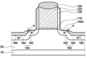
도 1a 내지 도 1h는 본 발명의 제1 실시예에 따른 반도체 집적 회로 장치의 제조 방법을 설명하기 위한 단면도들이다. 여기서는, NMOS 트랜지스터를 제조하는 것을 예로 들어 설명하였으나, 이에 한정되는 것은 아니다. 즉, PMOS 트랜지스터의 제조 과정에 적용하여도 무방하다.1A to 1H are cross-sectional views illustrating a method of manufacturing a semiconductor integrated circuit device according to a first embodiment of the present invention. Here, the manufacturing of the NMOS transistor is described as an example, but the present invention is not limited thereto. That is, the present invention may be applied to a manufacturing process of a PMOS transistor.
도 1a를 참조하면, 반도체 기판(10) 상에 소자 분리 영역을 형성하여 액티브 영역을 정의하고, 액티브 영역 상에 게이트 절연막(110)과 게이트(120)를 순차적으로 형성한다. 이어서, 액티브 영역 상에 P형 불순물을 주입하여 P웰(30)을 형성한다. 1A, an element isolation region is formed on a
구체적으로, 반도체 기판(10)은 실리콘 기판, SOI(Silicon On Insulator) 기판, 갈륨 비소 기판, 실리콘 게르마늄 기판, 세라믹 기판, 석영 기판, 또는 디스플레이용 유리 기판 등이 될 수 있고, 소자 분리 영역(20)은 LOCOS(LOCal Oxidation of Silicon)방법을 이용한 FOX(Field OXide) 또는 STI(Shallow Trench Isolation)가 될 수 있다. 또한, 게이트 절연막(110)은 예를 들어, SiO2, SiON, Si3N4, GexOyNz, GexSiyOz, 고유전율 물질 및 이들의 적층막이 사용될 수 있다. 여기서, 고유전율 물질은 HfO2, ZrO2, Al2O3, Ta2O5, 하프늄 실리케이트, 지르코늄 실리케이트 등이 될 수 있다. 또한, 게이트(120)는 예를 들어, 폴리 실리콘(poly Si), 불순물이 이온주입된 폴리 실리콘 등이 사용될 수 있다.Specifically, the
도 1b를 참조하면, 게이트(120)의 측벽에 스페이서 산화막(130)을 형성한다. 구체적으로, 게이트(120)가 형성된 반도체 기판(10) 전면에 산화막을 형성한 후 에치백(etch back)과 같은 전면 식각 공정을 이용하여, 게이트(120)의 측벽에 스페이서 산화막(130)을 형성한다.Referring to FIG. 1B, a
이어서, 스페이서 산화막(130)에 정렬된 제1 불순물 영역(162)을 형성한다. 구체적으로, 스페이서 산화막(130)을 이온 주입 마스크로 하여 N형 불순물, 예를 들어, 비소(As)를 주입할 수 있다. 여기서, 선택적으로 액티브 영역 내에 각각 할로 이온(halo ion)을 주입할 수 있다. 할로 이온은 채널 영역의 길이가 짧아짐에 따른 펀치 스루우 현상을 방지하기 위하여 게이트(120) 형성 후 반도체 기판(10)의 액티브 영역의 농도를 높이기 위하여 주입되는 이온을 의미한다. 할로 이온은 소오스/드레인 영역을 형성하기 위해 주입하는 이온과 반대 타입의 이온이 주로 사용된다. 따라서, 액티브 영역 내에는 P형 불순물, 예를 들어 붕소(B)를 주입할 수 있다.Then, a
이어서, 열공정을 실시한다. 열공정의 방식은 RTA(Rapid Thermal Annealing) 또는 LSA(LaSer Annealing) 등의 방식을 이용할 수 있다.Then, a thermal process is performed. Rapid Thermal Annealing (RTA) or LaSer Annealing (LSA) can be used for the definition of the thermal hole.
도 1c를 참조하면, 스페이서 산화막(130) 상에 형성된 스페이서 질화막(150)과, 반도체 기판(10)과 스페이서 질화막(150) 사이와 스페이서 산화막(130)과 스페이서 질화막(150) 사이에 형성된 접착 산화막(140)을 형성한다. 구체적으로, 게이트(120), 스페이서 산화막(130)이 형성된 반도체 기판(10) 전면에 산화막, 질화막을 형성한 후 에치백과 같은 전면 식각 공정을 이용하여, 상기 스페이서 질화막(150)과 접착 산화막(140)을 형성한다. 스페이서 질화막(150)이 게이트(120) 및 반도체 기판(10)과 잘 접착하지 않지 않기 때문에, 접착 산화막(140)을 반도체 기판(10)과 스페이서 질화막(150) 사이, 스페이서 산화막(130)과 스페이서 질화막(150) 사이에 L자 형태로 형성한다. 이와 동시에, 접착 산화막(140)은 게이트(120) 및 반도체 기판(10)이 스페이서 질화막(150)에 의해 받는 스트레스를 최소화시켜줄 수 있다. 즉, 접착 산화막(140)은 버퍼 역할도 하게 된다. 이러한 접착 산화막(140)은 예를 들어, LTO 일 수 있으나, 이에 한정되는 것은 아니다.1C, a
이어서, 스페이서 질화막(150)에 정렬된 제2 불순물 영역(164)을 형성한다. 구체적으로, 스페이서 질화막(150)을 이온 주입 마스크로 하여 N형 불순물, 예를 들어, 비소(As)를 주입할 수 있다. 제2 불순물 영역(164)은 제1 불순물 영역(162)보다 더 높은 도핑 농도를 갖고, 더 깊은 영역에 형성될 수 있다. 즉, 제1 및 제2 불순물 영역(162, 164)은 LDD(Lightly Diffused Drain) 구조의 소오스/드레인 영역(160)을 구성하게 된다. 도면으로 설명하지는 않았으나, NMOS 트랜지스터의 소오스/드레인 영역(160)은 다양한 구조로 변형 가능하며, 예를 들어, DDD(Double Diffused Drain), MIDDD(Mask Islanded Double Diffused Drain), MLDD(Mask LDD), LDMOS(Lateral Double-diffused MOS) 구조 등이 될 수 있다.Next, a
이어서, 열공정을 실시한다. 열공정의 방식은 RTA 또는 LSA 등의 방식을 이용할 수 있다.Then, a thermal process is performed. RTA or LSA can be used for the definition of the tangent hole.
도 1d를 참조하면, NMOS 트랜지스터 상에 블로킹 산화막(172)과 블로킹 질화막(174)을 순차적으로 형성한다.Referring to FIG. 1D, a blocking
구체적으로, 후속 단계에서 실리사이드막을 형성하는 공정을 실시하는데, 블로킹 산화막(172)과 블로킹 질화막(174)은 반도체 기판(10) 상에 실리사이드막을 형성하지 않을 부분을 블로킹하기 위한 것이다. 실리사이드막을 형성하지 않을 부분은 예를 들어, 고속 동작이 불필요한 MOS 트랜지스터일 수 있다.Specifically, in the subsequent step, a process of forming a silicide film is performed. The blocking
도 1e를 참조하면, NMOS 트랜지스터 상에 블로킹 질화막(174)을 식각한다. 즉, 도시된 NMOS 트랜지스터에는 후속 단계에서 실리사이드막을 형성할 것이므로, NMOS 트랜지스터 상에 있는 블로킹 질화막(174)을 제거하는 것이다.Referring to FIG. 1E, the blocking
특히, 본 발명의 제1 실시예에서, 블로킹 질화막(174)은 산화막에 대한 질화막의 선택비가 1을 초과하는 불산을 이용하여 제거할 수 있다. 전술한 바와 같이, 불산은 온도가 높아지거나 농도가 낮아질수록 산화막에 대한 질화막의 선택비가 높아진다. 여기서 사용되는 불산은, 예를 들어 약 65℃ 이상 약 85℃ 미만일 수 있고, 약 1000 : 1 ~ 약 2500 : 1로 희석할 수 있고, 더 자세하게는 약 1500 : 1 ~ 약 2000 : 1로 희석할 수 있다. 여기서, 블로킹 산화막(172)은 식각 정지막 역할을 한다. 따라서, 블로킹 산화막(172)은 산화막에 대한 질화막의 선택비가 1을 초과하는 불산에 의해 전부 제거되지 않고, 반도체 기판(10), 스페이서 질화막(150) 및/또는 게이트(120) 상에 잔류 산화막(172a)으로 남아있게 된다. Particularly, in the first embodiment of the present invention, the blocking
도 1f를 참조하면, NMOS 트랜지스터의 스페이서 질화막(150)을 제거한다. Referring to FIG. 1F, the
특히, 스페이서 질화막(150)은 산화막에 대한 질화막의 선택비가 1을 초과하는 불산을 이용하여 제거할 수 있다. In particular, the
또는, 산화막에 대한 질화막의 선택비가 1 미만인 불산을 이용하여 잔류 산화막(172a)을 먼저 제거하여 스페이서 질화막(150)이 노출되도록 하고, 이어서 산화막에 대한 질화막의 선택비가 1 초과인 불산을 이용하여 스페이서 질화막을 제거할 수도 있다.Alternatively, the
또는, 산화막에 대한 질화막의 선택비가 1 미만인 불산을 이용하여 잔류 산화막(172a)을 먼저 제거하여 스페이서 질화막(150)이 노출되도록 하고, 이어서 산화막에 대한 질화막의 선택비가 1 초과인 불산을 이용하여 스페이서 질화막을 제거하고, 이어서 산화막에 대한 질화막의 선택비가 1 미만인 불산을 이용하여 접착 산화막(140a)의 일부를 더 제거할 수도 있다.Alternatively, the
전술한 바와 같이, 불산은 온도가 높아지거나 농도가 낮아질수록 산화막에 대한 질화막의 선택비가 높아진다. 예를 들어, 산화막에 대한 질화막의 선택비가 1 초과하는 불산의 온도는 약 65℃ 이상 약 85℃ 미만일 수 있고, 약 1000 : 1 ~ 약 2500 : 1로 희석할 수 있고, 더 자세하게는 약 1500 : 1 ~ 약 2000 : 1로 희석할 수 있다. 산화막에 대한 질화막의 선택비가 1 미만의 불산의 온도는 예를 들어, 상온일 수 있고, 산화막에 대한 질화막의 선택비가 1 초과인 불산보다 덜 희석될 수 있다.As described above, the higher the temperature of the hydrofluoric acid or the lower the concentration thereof, the higher the selectivity of the nitride film to the oxide film. For example, the temperature of the hydrofluoric acid with a selectivity ratio of the nitride to oxide film of greater than 1 may be at least about 65 ° C and less than about 85 ° C, may be diluted to about 1000: 1 to about 2500: 1, 1 to about 2000: 1. The temperature of the hydrofluoric acid having a selectivity ratio of the nitride film to the oxide film of less than 1 may be, for example, room temperature and may be less diluted than hydrofluoric acid having a selectivity ratio of the nitride film to the oxide film of more than 1.
본 발명의 제1 실시예에서, NMOS 트랜지스터의 스페이서 질화막(150)을 제거하는 이유는 다음과 같다. 후속 단계에서 스트레스막(NMOS 트랜지스터 상에 인장 스트레스막, PMOS 트랜지스터 상에 압축 스트레스막)을 형성하는데(도 1h 참조), 스페이서 질화막(150)이 제거되면 스트레스막과 NMOS 트랜지스터의 채널 사이의 거리가 가까워지기 때문에, 스트레스 효과가 NMOS 트랜지스터의 채널에 잘 전달될 수 있다.In the first embodiment of the present invention, the reason why the
그런데, 스페이서 질화막(150)을 제거할 때, 반도체 기판(10) 상에 형성되어 있는 접착 산화막(140a)이 전부 제거되어서는 안 된다. 왜냐하면, 후속 단계에서 실리사이드막을 형성하는데(도 1g), 반도체 기판(10) 상에 형성되어 있는 접착 산화막(140a)이 없다면, 실리사이드막이 게이트에 매우 인접하여 형성된다. 이러한 경우, 누설 전류가 발생될 가능성이 높아지기 때문이다. 따라서, 스페이서 질화막(150)을 제거하되, 반도체 기판(10) 상에는 접착 산화막(140a)이 남아 있어야 한다.However, when the
도 1g를 참조하면, 제2 불순물 영역(164) 및/또는 게이트(120) 내에 실리사이드막(126, 166)을 형성한다.Referring to FIG. 1G,
구체적으로, 스페이서 질화막(150)이 제거된 NMOS 트랜지스터 상에 NiPt 또는 NiPt/TiN과 같은 금속막을 형성한다. 이후, RTA 또는 LSA과 같은 열공정을 하여 실리사이드막(126, 166)을 형성한다. 이후, 금속막을 제거한다. 선택적으로 다시, 열공정을 진행할 수 있다.Specifically, a metal film such as NiPt or NiPt / TiN is formed on the NMOS transistor from which the
특히, 본 발명의 제1 실시예에서, 실리사이드막(166)은 접착 산화막(140)과 일부 오버랩될 수 있다.Particularly, in the first embodiment of the present invention, the
도 1h를 참조하면, NMOS 트랜지스터 상에 식각 정지막(180)과 스트레스막(190)을 순차적으로 형성한다.Referring to FIG. 1H, an
구체적으로, 식각 정지막(180)은 LTO와 같은 산화막일 수 있고, 스트레스막(190)은 질화막일 수 있다. 스트레스막(190)으로 질화막을 쓰는 경우, N-H 본딩(bonding)과 Si-H 본딩의 비율에 따라 인장 스트레스(tensile stress)를 주게 되는지, 압축 스트레스(compressive stress)를 주게 되는지가 결정된다. 즉, N-H본딩/Si-H본딩의 비율이 약 1~5이면 인장 스트레스를 주게 되고, 약 5~20이면 압축 스트레스를 주게 된다. 인장 스트레스를 갖는 스트레스막(190)은 NMOS 트랜지스터의 동작 특성을 향상시켜 주고, 압축 스트레스를 갖는 스트레스막(190)은 PMOS 트랜지스터의 동작 특성을 향상시켜 준다. 따라서, 본 발명의 NMOS 트랜지스터 상에는 인장 스트레스를 갖는 스트레스막을 형성할 수 있다.Specifically, the
한편, 본 발명의 제1 실시예에서는 반도체 기판 상에 게이트를 형성하고(도 1a 참조), 게이트 측벽에 스페이서 산화막을 형성하고, 스페이서 산화막에 정렬된 제1 불순물 영역을 형성하고(도 1b 참조), 스페이서 산화막 상에 형성된 스페이서 질화막과, 반도체 기판과 스페이서 질화막 사이와 상기 스페이서 산화막과 스페이서 질화막 사이에 형성된 접착 산화막을 형성하고, 스페이서 질화막에 정렬된 제2 불순물 영역을 형성하고(도 1c 참조), 산화막에 대한 질화막의 선택비가 1 초과인 불산(hydrofluoric acid)를 이용하여 스페이서 질화막의 적어도 일부를 습식 식각하고(도 1f 참조), 제2 불순물 영역 내에 실리사이드막을 형성하고(도 1g 참조), 반도체 기판과 게이트 상에 식각 정지막과 스트레스막을 순차적으로 형성하는 것(도 1h 참조)으로 설명하였으나, 이에 한정되는 것은 아니다. In the first embodiment of the present invention, a gate is formed on the semiconductor substrate (see FIG. 1A), a spacer oxide film is formed on the gate sidewall, a first impurity region aligned with the spacer oxide film is formed (see FIG. , A spacer nitride film formed on the spacer oxide film, and an adhesion oxide film formed between the semiconductor substrate and the spacer nitride film and between the spacer oxide film and the spacer nitride film are formed to form a second impurity region aligned with the spacer nitride film (see FIG. At least a part of the spacer nitride film is wet-etched (see FIG. 1F) using hydrofluoric acid having a selectivity ratio of the nitride film to the oxide film of more than 1, and a silicide film is formed in the second impurity region And the etching stopper film and the stress film are sequentially formed on the gate (refer to FIG. 1H). However, But is not limited thereto.
즉, 어떠한 방식으로 만들어졌는지에 상관없이, 게이트와, 게이트의 측벽에 형성된 질화막과, 반도체 기판과 질화막 사이와 게이트와 질화막 사이에 산화막이 있는 반도체 소자를 제공하고, 산화막에 대한 질화막의 선택비가 1 초과인 불산을 이용하여 상기 반도체 소자에 식각 공정을 진행할 수 있음은, 본 발명이 속하는 기술의 당업자에게 자명하다.That is, regardless of how it is made, it is possible to provide a semiconductor device having a gate, a nitride film formed on a sidewall of a gate, a semiconductor substrate, a nitride film, and an oxide film between the gate and the nitride film, It is apparent to those skilled in the art that the etching process can be carried out on the semiconductor device by using hydrofluoric acid in excess.
도 2a 내지 도 2c는 본 발명의 제2 실시예에 따른 반도체 집적 회로 장치의 제조 방법을 설명하기 위한 단면도들이다. 본 발명의 제2 실시예는 스페이서 질화막을 제거하는 과정이 제1 실시예와 차이가 있으므로, 이에 대해서 도 2a 내지 도 2c를 참조하여 자세히 설명하도록 한다.2A to 2C are cross-sectional views illustrating a method of manufacturing a semiconductor integrated circuit device according to a second embodiment of the present invention. The second embodiment of the present invention differs from the first embodiment in the process of removing the spacer nitride film, which will be described in detail with reference to FIGS. 2A to 2C.
도 2a를 참조하면, NMOS 트랜지스터의 스페이서 질화막(150)의 일부를 제거한다. Referring to FIG. 2A, a part of the
특히, 스페이서 질화막(150)은 산화막에 대한 질화막의 선택비가 1을 초과하는 불산을 이용하여 제거할 수 있다. In particular, the
또는, 산화막에 대한 질화막의 선택비가 1 미만인 불산을 이용하여 잔류 산화막(172a)을 먼저 제거하여 스페이서 질화막(150)이 노출되도록 하고, 이어서 산화막에 대한 질화막의 선택비가 1 초과인 불산을 이용하여 스페이서 질화막을 제거할 수도 있다.Alternatively, the
도 2b를 참조하면, 제2 불순물 영역(164) 및/또는 게이트(120) 내에 실리사이드막(126, 166)을 형성한다.Referring to FIG. 2B, the
도 2c를 참조하면, RIE(Reactive Ion Etching)를 이용하여 잔류하는 스페이서 질화막(150)을 식각한다.Referring to FIG. 2C, the remaining
도 3a 및 도 3b는 본 발명의 제3 실시예에 따른 반도체 집적 회로 장치의 제조 방법을 설명하기 위한 단면도들이다.3A and 3B are cross-sectional views illustrating a method of manufacturing a semiconductor integrated circuit device according to a third embodiment of the present invention.
도 3a를 참조하면, 반도체 기판(10) 상에 NMOS 및 PMOS 트랜지스터를 형성한다. NMOS 트랜지스터는 도 1a 내지 도 1h를 통해서 설명한 방법을 통해서 형성하고, PMOS 트랜지스터도 상기 NMOS 트랜지스터의 제조 방법과 유사한 방법을 이용하여 형성한다. PMOS 트랜지스터에서 설명되지 않는 도면부호는 다음과 같다. 40은 N웰, 220은 게이트, 230은 스페이서 산화막, 240a는 접착 산화막, 260은 소오스/드레인 영역, 262는 제1 불순물 영역, 264는 제2 불순물 영역, 226, 266은 실리사이드막을 나타낸다.Referring to FIG. 3A, NMOS and PMOS transistors are formed on a
이어서, NMOS 및 PMOS 트랜지스터 상에는 도 1h과 같은 식각 정지막(180)과 스트레스막(190)을 형성한다. 스트레스막(190)으로 질화막을 쓰는 경우, N-H 본딩(bonding)과 Si-H 본딩의 비율에 따라 인장 스트레스를 주게 되는지, 압축 스트레스를 주게 되는지가 결정된다. 인장 스트레스를 갖는 스트레스막은 NMOS 트랜지스터의 동작 특성을 향상시켜 주고, 압축 스트레스를 갖는 스트레스막은 PMOS 트랜지스터의 동작 특성을 향상시켜 준다. 반면, PMOS 트랜지스터 상에 인장 스트레스를 주는 스트레스막이 형성되어 있으면, PMOS 트랜지스터의 동작 특성을 떨어뜨린다. 따라서, 스트레스막(174)이 인장 스트레스를 갖는 경우, PMOS 트랜지스터 상에 형성된 스트레스막(190)을 제거해야 한다.Next, an
도 3b를 참조하면, PMOS 트랜지스터 상에 형성된 스트레스막(190)을 제거한다.Referring to FIG. 3B, the
구체적으로, 반도체 기판(10) 상에 NMOS 트랜지스터를 마스킹하는 포토레지스트 패턴(195)을 형성하고, 산화막에 대한 질화막의 선택비가 1초과인 불산을 이용하여, PMOS 트랜지스터 상에 형성된 스트레스막(190)을 제거한다. 전술한 바와 같이, 산화막에 대한 질화막의 선택비가 1 초과하는 불산의 온도는 약 65℃ 이상 약 85℃ 미만일 수 있고, 약 1000 : 1 ~ 약 2500 : 1로 희석할 수 있고, 더 자세하게는 약 1500 : 1 ~ 약 2000 : 1로 희석할 수 있다.Specifically, a
도 4a 내지 도 4d는 본 발명의 제4 실시예에 따른 반도체 집적 회로 장치의 제조 방법을 설명하기 위한 단면도들이다.4A to 4D are cross-sectional views illustrating a method for fabricating a semiconductor integrated circuit device according to a fourth embodiment of the present invention.
도 4a를 참조하면, 반도체 기판(11) 내에 트렌치(330)를 형성한다.Referring to FIG. 4A, a
자세히 설명하면, 반도체 기판(11) 상에 트렌치를 정의하는 패드 산화막(310), 패드 질화막(320)을 순차적으로 형성한다. 패드 산화막(310)은 산화(oxidation) 방식을 이용하여 약 40∼150Å의 두께로 성장시킬 수 있고, 패드 질화막(320)은 패드 산화막(310) 상에 LPCVD(Low Pressure Chemical Vapor Deposition) 방식을 이용하여 약 600∼1500Å의 두께로 적층시킬 수 있다. 여기서, 패드 산화막(310)은 반도체 기판(11)과 패드 질화막(320) 사이의 스트레스를 완화시켜 준다. 패드 질화막(320)은 트렌치(330)의 형성시 식각 마스크로서 사용되며, 후속 단계의 CMP 공정에서 식각 정지막의 역할도 한다.In detail, a
이어서, 패드 질화막(320)을 식각 마스크로 이용하여 3000Å 정도의 얕은 깊이로 트렌치(330)를 형성한다. 예를 들어, RIE(Reactive Ion Etching)을 이용하여 트렌치(330)를 형성할 수 있다.Next, the
도 4b를 참조하면, 트렌치(330)를 따라 라이너 산화막(340)을 컨포말하게(conformally) 형성한다.Referring to FIG. 4B, the
자세히 설명하면, 트렌치(330)의 내벽에 라이너 산화막(340), 예를 들어 산화막을 약 800~900℃의 온도에서 산화 방식을 이용하여 약 100∼400Å의 두께로 성장시킨다. 라이너 산화막(340)은 트렌치(330)의 내벽에, 식각에 의해 존재하는 손상된 실리콘 격자를 치유한다.In detail, a
도 4c를 참조하면, 라이너 산화막(340) 및 패드 질화막(320)을 따라 트렌치(330)를 따라 라이너 질화막(350)을 컨포말하게 형성한다.Referring to FIG. 4C, the
자세히 설명하면, 라이너 질화막(350)은 LPCVD 방식을 이용하여 약 70~300Å의 두께로 적층시킨다. More specifically, the
도 4d를 참조하면, 라이너 질화막(350) 상에 트렌치(330)가 매립되도록 매립 산화막(360)을 형성한다.Referring to FIG. 4D, a buried
자세히 설명하면, 우선 트렌치를 매립하기 충분한 두께로 반도체 기판(11) 상에 산화막을 형성한다. 이 때, 트렌치(330) 내의 절연막에는 빈 공간, 즉 보이드(void)가 존재하지 않는 것이 바람직하다. 반도체 소자의 설계 룰(design rule)에 따라 다소 차이가 있지만, O3-TEOS(Tetra Ortho Silicate Glass) APCVD(Atmospheric Pressure Chemical Vapor Deposition)이나 PECVD(Plasma Enhanced Chemical Vapor Deposition) 방식 또는 HDP CVD(High Density Plasma Chemical Vapor Deposition) 방식에 의해 형성할 수 있다.More specifically, an oxide film is first formed on the
이어서, CMP 방식을 이용하여 평탄화한다. 선택적으로, 열공정을 진행할 수 있다.Then, planarization is performed using a CMP method. Optionally, a thermal process can proceed.
도 4e를 참조하면, 패드 질화막(320)의 상면이 노출되도록 매립 산화막(360)의 일부와 라이너 질화막(350)의 일부는 식각한다. 특히, 본 발명의 제4 실시예에서는 매립 산화막(360)의 일부를 제거하여 매립 산화막(360)의 높이를 낮추는 것과, 라이너 질화막(350)의 일부를 식각하는 것을 동시에 진행한다. Referring to FIG. 4E, a portion of the buried
자세히 설명하면, 산화막에 대한 질화막의 선택비가 약 0.7 이상 약 1.4 미만인 불산을 이용하여 매립 산화막(360)의 일부와 라이너 질화막(350)의 일부를 식각한다. 산화막에 대한 질화막의 선택비는 약 1일수도 있다. 예를 들어, 이러한 불산은 온도가 약 65℃ 이상 85℃ 미만이고, 농도는 약 300:1 정도일 수 있다.More specifically, a part of the buried
도 4f를 참조하면, 패드 질화막(320)을 제거하여, 패드 산화막(310)이 드러나도록 할 수 있다.Referring to FIG. 4F, the
인산을 이용하여 패드 질화막(320)을 제거할 수 있다.The
또는, 산화막에 대한 질화막의 선택비가 약 10 ~ 약 50인 불산을 이용하여 패드 질화막(320)을 제거할 수 있다. 이러한 불산의 온도는 약 65℃ 이상 85℃ 미만일 수 있다. 또한, 산화막에 대한 질화막의 선택비를 충분히 올리기 위해서는 불산을 약 1000:1 ~ 약 2500:1 로 희석할 수 있고, 더 자세하게는 약 1500 : 1 ~ 약 2000 : 1로 희석할 수 있다.Alternatively, the
도 5는 본 발명의 제5 실시예에 따른 반도체 집적 회로 장치의 제조 방법을 설명하기 위한 도면이다. 본 발명의 제 5실시예는 전술한 매립 산화막의 일부 및 라이너 질화막의 일부를 제거하는 단계(도 4e 참조), 패드 산화막을 제거하는 단계(도 4f 참조)를 하나의 배스 내에서 연속적으로 실시한다는 점이, 제4 실시예와 다르다.5 is a view for explaining a method of manufacturing a semiconductor integrated circuit device according to a fifth embodiment of the present invention. The fifth embodiment of the present invention is characterized in that a step of removing a part of the buried oxide film and a part of the liner nitride film (see FIG. 4E) and a step of removing the pad oxide film (see FIG. 4F) This is different from the fourth embodiment.
도 5를 참조하면, 반도체 제조 설비(400)는 배스(bath)(410), 불소 저장부(420), 밸브(422), 초순수(DI) 저장부(430), 밸브(432)를 포함한다.5, the
우선, 반도체 기판(W) 상에 순차적으로 형성된 패드 산화막 및 패드 질화막과, 패드 산화막 및 패드 질화막을 식각 마스크로 이용하여 반도체 기판(W) 내에 형성된 트렌치와, 트렌치를 따라 컨포말하게 형성된 라이너 산화막과, 라이너 산화막 및 패드 질화막을 따라 컨포말하게 형성된 라이너 질화막과, 라이너 질화막 상에 트렌치가 매립되도록 형성된 매립 산화막을 포함하는 반도체 기판(W)을 배스(410)에 위치시킨다.First, a trench formed in the semiconductor substrate W using a pad oxide film and a pad nitride film sequentially formed on the semiconductor substrate W, a pad oxide film and a pad nitride film as an etching mask, a liner oxide film formed in conformity with the trench, , A liner nitride film formed conformally along the liner oxide film and the pad nitride film, and a buried oxide film formed so as to be buried in the trench on the liner nitride film are placed in the
이어서, 배스(410) 내에서 불산의 온도 및/또는 농도를 변화시켜가면서, 매립 산화막의 일부, 라이너 질화막의 일부, 패드 질화막을 식각하게 된다.Then, a part of the buried oxide film, a part of the liner nitride film, and the pad nitride film are etched while changing the temperature and / or the concentration of the hydrofluoric acid in the
즉, 패드 질화막의 상면이 노출되도록 매립 산화막의 일부, 라이너 질화막의 일부를 제거하는 단계에서 사용되는 불산은, 산화막에 대한 질화막의 선택비가 약 0.7 ~ 약 1.4가 되도록, 밸브(422, 432)를 조절함으로써 불산의 농도를 조절한다. 예를 들어, 불산의 농도는 약 300:1 정도일 수 있다. That is, the hydrofluoric acid used in the step of removing a part of the buried oxide film and a part of the liner nitride film such that the top surface of the pad nitride film is exposed may be formed of the
이어서, 패드 질화막을 제거하는 단계에서 사용되는 불산은, 산화막에 대한 질화막의 선택비가 약 10 ~ 약 50이 되도록, 밸브(422, 432)를 조절함으로써 불산의 농도를 조절한다. 예를 들어, 불산의 농도는 약 1000:1 ~ 약 2500:1 일 수 있고, 더 자세하게는 약 1500 : 1 ~ 약 2000 : 1일 수 있다. Subsequently, the hydrofluoric acid used in the step of removing the pad nitride film controls the concentration of hydrofluoric acid by adjusting the
다만, 이러한 농도의 수치는 예시적인 것에 불과하나, 매립 산화막의 일부, 라이너 질화막의 일부를 제거하는 단계에서 사용되는 불산보다 농도가 낮도록 조절할 수 있다. However, such a concentration value is only an example, but the concentration can be adjusted to be lower than that of hydrofluoric acid used in the step of removing a part of the buried oxide film and a part of the liner nitride film.
또한, 본 발명의 제5 실시예에서는, 패드 질화막을 제거하는 단계의 불산과, 매립 산화막의 일부, 라이너 질화막의 일부를 제거하는 단계의 불산의 온도는 동일한 것을 예로 들었으나, 이에 한정되는 것은 아니다. 즉, 산화막에 대한 질화막의 선택비를 높이기 위해서, 매립 산화막의 일부, 라이너 질화막의 일부를 제거하는 단계에서는 불산의 온도를 더 높여도 무방하다.In the fifth embodiment of the present invention, the hydrofluoric acid at the step of removing the pad nitride film, the portion of the buried oxide film and the portion of the liner nitride film are removed at the same temperature, but the present invention is not limited thereto . That is, in order to increase the selectivity of the nitride film to the oxide film, the temperature of the hydrofluoric acid may be increased in the step of removing a part of the buried oxide film and a part of the liner nitride film.
본 발명의 제5 실시예에서는, 불산의 농도를 2번 조절하는 것(즉, 매립 산화막의 일부, 라이너 질화막의 일부를 제거하는 단계, 패드 질화막을 제거하는 단계에서 각각 농도를 조절함)로 나누어 설명하였으나, 본 발명의 권리 범위는 이에 한정되는 것은 아니다. 즉, 하나의 배스 내에 반도체 기판(W)을 위치시키고, 불산의 온도 및/또는 농도를 3번 이상 조절하여 불산의 산화막에 대한 질화막의 선택비를 3번 이상 조절함으로써, 매립 산화막의 일부, 라이너 질화막의 일부, 패드 질화막을 제거하여도 무방하다.In the fifth embodiment of the present invention, the concentration of hydrofluoric acid is adjusted by two times (i.e., the concentration of the buried oxide film, the portion of the liner nitride film, and the concentration of the pad nitride film are removed) The scope of rights of the present invention is not limited thereto. That is, by positioning the semiconductor substrate W in one bath and adjusting the temperature and / or concentration of the hydrofluoric acid three or more times to adjust the selection ratio of the nitride film to the hydrofluoric acid film three or more times, A part of the nitride film, and the pad nitride film may be removed.
또한, 반도체 제조 설비(400)는 배치 타입(batch type)일 수도 있고, 싱글 타입(single type)일 수도 있다.In addition, the
이상 첨부된 도면을 참조하여 본 발명의 실시예를 설명하였지만, 본 발명이 속하는 기술분야에서 통상의 지식을 가진 자는 본 발명이 그 기술적 사상이나 필수적인 특징을 변경하지 않고서 다른 구체적인 형태로 실시될 수 있다는 것을 이해할 수 있을 것이다. 그러므로 이상에서 기술한 실시예들은 모든 면에서 예시적인 것이며 한정적이 아닌 것으로 이해해야만 한다. While the present invention has been described in connection with what is presently considered to be practical exemplary embodiments, it is to be understood that the invention is not limited to the disclosed embodiments, but, on the contrary, You will understand. It is therefore to be understood that the above-described embodiments are illustrative in all aspects and not restrictive.
도 1a 내지 도 1h는 본 발명의 제1 실시예에 따른 반도체 집적 회로 장치의 제조 방법을 설명하기 위한 단면도들이다.1A to 1H are cross-sectional views illustrating a method of manufacturing a semiconductor integrated circuit device according to a first embodiment of the present invention.
도 2a 내지 도 2c는 본 발명의 제2 실시예에 따른 반도체 집적 회로 장치의 제조 방법을 설명하기 위한 단면도들이다.2A to 2C are cross-sectional views illustrating a method of manufacturing a semiconductor integrated circuit device according to a second embodiment of the present invention.
도 3a 및 도 3b는 본 발명의 제3 실시예에 따른 반도체 집적 회로 장치의 제조 방법을 설명하기 위한 단면도들이다.3A and 3B are cross-sectional views illustrating a method of manufacturing a semiconductor integrated circuit device according to a third embodiment of the present invention.
도 4a 내지 도 4f는 본 발명의 제4 실시예에 따른 반도체 집적 회로 장치의 제조 방법을 설명하기 위한 단면도들이다.4A to 4F are cross-sectional views illustrating a method for fabricating a semiconductor integrated circuit device according to a fourth embodiment of the present invention.
도 5는 본 발명의 제5 실시예에 따른 반도체 집적 회로 장치의 제조 방법을 설명하기 위한 도면이다. 5 is a view for explaining a method of manufacturing a semiconductor integrated circuit device according to a fifth embodiment of the present invention.
(도면의 주요부분에 대한 부호의 설명)DESCRIPTION OF THE REFERENCE NUMERALS (S)
110 : 게이트 절연막 120 : 게이트110: gate insulating film 120: gate
130 : 스페이서 산화막 140 : 접착 산화막130: spacer oxide film 140:
150 : 스페이서 질화막 160 : 소오스/드레인 영역150: spacer nitride film 160: source / drain region
172 : 블로킹 산화막 174 : 블로킹 질화막172: blocking oxide film 174: blocking nitride film
180 : 식각 정지막 190 : 스트레스막180: etch stop film 190: stress film
310 : 패드 산화막 320 : 패드 질화막310: pad oxide film 320: pad nitride film
330 : 트렌치 340 : 라이너 산화막330: trench 340: liner oxide film
350 : 라이너 질화막 360 : 매립 산화막350: liner nitride film 360: buried oxide film
410 : 배스 420 : 불소 저장부410: Bath 420: Fluorine storage part
430 : 초순수 저장부430: ultrapure water storage part
Claims (35)
Applications Claiming Priority (2)
| Application Number | Priority Date | Filing Date | Title |
|---|---|---|---|
| US11/858,535 US7902082B2 (en) | 2007-09-20 | 2007-09-20 | Method of forming field effect transistors using diluted hydrofluoric acid to remove sacrificial nitride spacers |
| US11/858,535 | 2007-09-20 |
Publications (2)
| Publication Number | Publication Date |
|---|---|
| KR20090031216A KR20090031216A (en) | 2009-03-25 |
| KR101591855B1 true KR101591855B1 (en) | 2016-02-05 |
Family
ID=40472110
Family Applications (1)
| Application Number | Title | Priority Date | Filing Date |
|---|---|---|---|
| KR1020080079538A KR101591855B1 (en) | 2007-09-20 | 2008-08-13 | Fabricating method for semiconductor integrated circuit device |
Country Status (4)
| Country | Link |
|---|---|
| US (1) | US7902082B2 (en) |
| JP (2) | JP5441366B2 (en) |
| KR (1) | KR101591855B1 (en) |
| SG (1) | SG151194A1 (en) |
Families Citing this family (13)
| Publication number | Priority date | Publication date | Assignee | Title |
|---|---|---|---|---|
| DE102008030854B4 (en) * | 2008-06-30 | 2014-03-20 | Advanced Micro Devices, Inc. | MOS transistors having depressed drain and source regions and non-conforming metal silicide regions, and methods of fabricating the transistors |
| JP2012186187A (en) * | 2009-07-08 | 2012-09-27 | Sharp Corp | Etching method and etching process device |
| CN102856179B (en) * | 2011-06-29 | 2015-09-02 | 中芯国际集成电路制造(上海)有限公司 | The formation method of semiconductor device |
| US9087915B2 (en) * | 2011-12-06 | 2015-07-21 | Intel Corporation | Interlayer dielectric for non-planar transistors |
| KR101887144B1 (en) | 2012-03-15 | 2018-08-09 | 삼성전자주식회사 | Semiconductor device and Method of manufacturing the same |
| US8652917B2 (en) * | 2012-05-23 | 2014-02-18 | GlobalFoundries, Inc. | Superior stability of characteristics of transistors having an early formed high-K metal gate |
| KR101921465B1 (en) | 2012-08-22 | 2018-11-26 | 삼성전자 주식회사 | Semiconductor device and method for fabricating the same |
| US8716136B1 (en) * | 2012-10-19 | 2014-05-06 | Globalfoundries Inc. | Method of forming a semiconductor structure including a wet etch process for removing silicon nitride |
| JP6221155B2 (en) * | 2013-12-11 | 2017-11-01 | 株式会社Screenホールディングス | Substrate processing method and substrate processing apparatus |
| CN109103253B (en) * | 2017-06-21 | 2022-05-20 | 比亚迪半导体股份有限公司 | MOS type power device and preparation method thereof |
| US10355100B1 (en) | 2018-05-17 | 2019-07-16 | Sandisk Technologies Llc | Field effect transistors having different stress control liners and method of making the same |
| CN113322071A (en) * | 2021-05-28 | 2021-08-31 | 长江存储科技有限责任公司 | Etching composition and method of use thereof |
| JP7429211B2 (en) * | 2021-09-16 | 2024-02-07 | 合肥晶合集成電路股▲ふん▼有限公司 | Semiconductor device and method for manufacturing semiconductor device |
Citations (2)
| Publication number | Priority date | Publication date | Assignee | Title |
|---|---|---|---|---|
| JP2001176839A (en) * | 1999-12-20 | 2001-06-29 | Fujitsu Ltd | Manufacturing method of semiconductor device |
| WO2007054403A1 (en) * | 2005-11-14 | 2007-05-18 | International Business Machines Corporation | Structure and method to increase strain enhancement with spacerless fet and dual liner process |
Family Cites Families (69)
| Publication number | Priority date | Publication date | Assignee | Title |
|---|---|---|---|---|
| JPH0529297A (en) * | 1991-07-24 | 1993-02-05 | Matsushita Electric Ind Co Ltd | Wet etching device |
| JPH06163509A (en) * | 1992-07-27 | 1994-06-10 | Mitsubishi Kasei Corp | Control method for etching liquid |
| US5310457A (en) * | 1992-09-30 | 1994-05-10 | At&T Bell Laboratories | Method of integrated circuit fabrication including selective etching of silicon and silicon compounds |
| JP3321864B2 (en) | 1992-11-24 | 2002-09-09 | ヤマハ株式会社 | Semiconductor device and its manufacturing method. |
| JP3307489B2 (en) * | 1993-12-09 | 2002-07-24 | 三菱電機株式会社 | Semiconductor device and manufacturing method thereof |
| KR970001869B1 (en) | 1994-11-08 | 1997-02-17 | 대우통신 주식회사 | Method for offering the position data of the portable terminal |
| KR0183785B1 (en) | 1995-12-22 | 1999-03-20 | 윤종용 | Method of manufacturing mos transistor |
| US6657229B1 (en) * | 1996-05-28 | 2003-12-02 | United Microelectronics Corporation | Semiconductor device having multiple transistors sharing a common gate |
| GB9618620D0 (en) | 1996-09-06 | 1996-10-16 | Electrotech Equipments Ltd | A method of forming a layer |
| US6184157B1 (en) * | 1998-06-01 | 2001-02-06 | Sharp Laboratories Of America, Inc. | Stress-loaded film and method for same |
| KR100327342B1 (en) | 1999-10-27 | 2002-03-06 | 윤종용 | Composite etchant for a nitride etching in a semiconductor process and an etching method using the same etchant |
| KR20010076522A (en) | 2000-01-26 | 2001-08-16 | 윤종용 | The apparatus for fabricating semiconductor devices |
| US6372589B1 (en) * | 2000-04-19 | 2002-04-16 | Advanced Micro Devices, Inc. | Method of forming ultra-shallow source/drain extension by impurity diffusion from doped dielectric spacer |
| JP4167381B2 (en) | 2000-06-08 | 2008-10-15 | 松下電器産業株式会社 | Manufacturing method of semiconductor device |
| KR100375229B1 (en) * | 2000-07-10 | 2003-03-08 | 삼성전자주식회사 | Trench isolation method |
| KR20020017845A (en) | 2000-08-31 | 2002-03-07 | 박종섭 | A method for forming a bit line of a semiconductor device |
| KR20020074551A (en) | 2001-03-20 | 2002-10-04 | 삼성전자 주식회사 | Method of forming a metal line in a semiconductor device |
| JP2002289682A (en) * | 2001-03-28 | 2002-10-04 | Nec Corp | Semiconductor device and its manufacturing method |
| EP1386350A1 (en) * | 2001-04-27 | 2004-02-04 | Koninklijke Philips Electronics N.V. | Method of wet etching an inorganic antireflection layer |
| JP2003060076A (en) | 2001-08-21 | 2003-02-28 | Nec Corp | Semiconductor device and manufacturing method therefor |
| JP2003086704A (en) | 2001-09-14 | 2003-03-20 | Matsushita Electric Ind Co Ltd | Semiconductor device and manufacturing method thereof |
| JP4173672B2 (en) | 2002-03-19 | 2008-10-29 | 株式会社ルネサステクノロジ | Semiconductor device and manufacturing method thereof |
| US20030209326A1 (en) | 2002-05-07 | 2003-11-13 | Mattson Technology, Inc. | Process and system for heating semiconductor substrates in a processing chamber containing a susceptor |
| JP2004047608A (en) | 2002-07-10 | 2004-02-12 | Toshiba Corp | Semiconductor device and its manufacture |
| JP2004071928A (en) * | 2002-08-08 | 2004-03-04 | Renesas Technology Corp | Manufacturing method for semiconductor device |
| JP3980985B2 (en) | 2002-10-04 | 2007-09-26 | 株式会社東芝 | Semiconductor device and manufacturing method thereof |
| JP3974028B2 (en) * | 2002-11-29 | 2007-09-12 | 株式会社東芝 | Manufacturing method of semiconductor device |
| US7022561B2 (en) * | 2002-12-02 | 2006-04-04 | Taiwan Semiconductor Manufacturing Company, Ltd. | CMOS device |
| KR100498644B1 (en) | 2003-02-04 | 2005-07-01 | 동부아남반도체 주식회사 | Method for manufacturing semiconductor device with pip capacitor |
| JP4015068B2 (en) * | 2003-06-17 | 2007-11-28 | 株式会社東芝 | Manufacturing method of semiconductor device |
| JP2005064314A (en) | 2003-08-18 | 2005-03-10 | Seiko Epson Corp | Semiconductor device and method for manufacturing the same |
| US20050048732A1 (en) * | 2003-08-26 | 2005-03-03 | International Business Machines Corporation | Method to produce transistor having reduced gate height |
| US6869866B1 (en) * | 2003-09-22 | 2005-03-22 | International Business Machines Corporation | Silicide proximity structures for CMOS device performance improvements |
| US6939814B2 (en) * | 2003-10-30 | 2005-09-06 | International Business Machines Corporation | Increasing carrier mobility in NFET and PFET transistors on a common wafer |
| US7015082B2 (en) * | 2003-11-06 | 2006-03-21 | International Business Machines Corporation | High mobility CMOS circuits |
| KR101026472B1 (en) | 2003-11-19 | 2011-04-01 | 매그나칩 반도체 유한회사 | Method for forming gate of semiconductor device |
| JP3811697B2 (en) * | 2003-11-19 | 2006-08-23 | 松下電器産業株式会社 | Manufacturing method of semiconductor device |
| KR100616499B1 (en) | 2003-11-21 | 2006-08-28 | 주식회사 하이닉스반도체 | Method for fabrication of semiconductor device |
| US7052946B2 (en) * | 2004-03-10 | 2006-05-30 | Taiwan Semiconductor Manufacturing Co. Ltd. | Method for selectively stressing MOSFETs to improve charge carrier mobility |
| TWI252539B (en) * | 2004-03-12 | 2006-04-01 | Toshiba Corp | Semiconductor device and manufacturing method therefor |
| KR101025761B1 (en) * | 2004-03-30 | 2011-04-04 | 삼성전자주식회사 | Semiconductor Integrated circuit and method of manufacturing the same |
| US7190033B2 (en) * | 2004-04-15 | 2007-03-13 | Taiwan Semiconductor Manufacturing Company, Ltd. | CMOS device and method of manufacture |
| KR20060000912A (en) | 2004-06-30 | 2006-01-06 | 주식회사 하이닉스반도체 | Method for fabrication of semiconductor device |
| JP4444027B2 (en) | 2004-07-08 | 2010-03-31 | 富士通マイクロエレクトロニクス株式会社 | N-channel MOS transistor and CMOS integrated circuit device |
| US20060011586A1 (en) * | 2004-07-14 | 2006-01-19 | Shea Kevin R | Method of etching nitrides |
| JP2006041118A (en) * | 2004-07-26 | 2006-02-09 | Toshiba Corp | Semiconductor device and method of manufacturing same |
| DE102004042167B4 (en) * | 2004-08-31 | 2009-04-02 | Advanced Micro Devices, Inc., Sunnyvale | A method of forming a semiconductor structure comprising transistor elements having differently strained channel regions, and corresponding semiconductor structure |
| JP4794838B2 (en) | 2004-09-07 | 2011-10-19 | 富士通セミコンダクター株式会社 | Semiconductor device and manufacturing method thereof |
| DE102004052617B4 (en) * | 2004-10-29 | 2010-08-05 | Advanced Micro Devices, Inc., Sunnyvale | A method of manufacturing a semiconductor device and semiconductor device having semiconductor regions having differently deformed channel regions |
| DE102004052578B4 (en) * | 2004-10-29 | 2009-11-26 | Advanced Micro Devices, Inc., Sunnyvale | A method of creating a different mechanical strain in different channel regions by forming an etch stop layer stack having differently modified internal stress |
| US7344934B2 (en) * | 2004-12-06 | 2008-03-18 | Infineon Technologies Ag | CMOS transistor and method of manufacture thereof |
| JP5002891B2 (en) | 2004-12-17 | 2012-08-15 | 富士通セミコンダクター株式会社 | Manufacturing method of semiconductor device |
| JP4453572B2 (en) | 2005-02-22 | 2010-04-21 | ソニー株式会社 | Manufacturing method of semiconductor integrated circuit |
| US7229869B2 (en) * | 2005-03-08 | 2007-06-12 | Texas Instruments Incorporated | Method for manufacturing a semiconductor device using a sidewall spacer etchback |
| JP2006324278A (en) | 2005-05-17 | 2006-11-30 | Sony Corp | Semiconductor device and manufacturing method thereof |
| US7569888B2 (en) * | 2005-08-10 | 2009-08-04 | Toshiba America Electronic Components, Inc. | Semiconductor device with close stress liner film and method of manufacturing the same |
| US7297584B2 (en) * | 2005-10-07 | 2007-11-20 | Samsung Electronics Co., Ltd. | Methods of fabricating semiconductor devices having a dual stress liner |
| JP5091397B2 (en) * | 2005-10-27 | 2012-12-05 | パナソニック株式会社 | Semiconductor device |
| US20070099360A1 (en) * | 2005-11-03 | 2007-05-03 | International Business Machines Corporation | Integrated circuits having strained channel field effect transistors and methods of making |
| US7759206B2 (en) * | 2005-11-29 | 2010-07-20 | International Business Machines Corporation | Methods of forming semiconductor devices using embedded L-shape spacers |
| US7521307B2 (en) * | 2006-04-28 | 2009-04-21 | International Business Machines Corporation | CMOS structures and methods using self-aligned dual stressed layers |
| US7719089B2 (en) * | 2006-05-05 | 2010-05-18 | Sony Corporation | MOSFET having a channel region with enhanced flexure-induced stress |
| US7585720B2 (en) * | 2006-07-05 | 2009-09-08 | Toshiba America Electronic Components, Inc. | Dual stress liner device and method |
| US20080026523A1 (en) * | 2006-07-28 | 2008-01-31 | Chartered Semiconductor Manufacturing, Ltd And International Business Machines Corporation (Ibm) | Structure and method to implement dual stressor layers with improved silicide control |
| US7482215B2 (en) * | 2006-08-30 | 2009-01-27 | International Business Machines Corporation | Self-aligned dual segment liner and method of manufacturing the same |
| KR100773352B1 (en) * | 2006-09-25 | 2007-11-05 | 삼성전자주식회사 | Method of fabricating semiconductor device having stress enhanced mos transistor and semiconductor device fabricated thereby |
| US7534678B2 (en) * | 2007-03-27 | 2009-05-19 | Samsung Electronics Co., Ltd. | Methods of forming CMOS integrated circuit devices having stressed NMOS and PMOS channel regions therein and circuits formed thereby |
| US7521314B2 (en) * | 2007-04-20 | 2009-04-21 | Freescale Semiconductor, Inc. | Method for selective removal of a layer |
| JP2009099724A (en) * | 2007-10-16 | 2009-05-07 | Toshiba Corp | Semiconductor device |
-
2007
- 2007-09-20 US US11/858,535 patent/US7902082B2/en active Active
-
2008
- 2008-06-18 JP JP2008158931A patent/JP5441366B2/en active Active
- 2008-08-13 KR KR1020080079538A patent/KR101591855B1/en active IP Right Grant
- 2008-09-10 SG SG200806625-0A patent/SG151194A1/en unknown
-
2013
- 2013-04-16 JP JP2013085597A patent/JP5981385B2/en active Active
Patent Citations (2)
| Publication number | Priority date | Publication date | Assignee | Title |
|---|---|---|---|---|
| JP2001176839A (en) * | 1999-12-20 | 2001-06-29 | Fujitsu Ltd | Manufacturing method of semiconductor device |
| WO2007054403A1 (en) * | 2005-11-14 | 2007-05-18 | International Business Machines Corporation | Structure and method to increase strain enhancement with spacerless fet and dual liner process |
Also Published As
| Publication number | Publication date |
|---|---|
| JP2009076857A (en) | 2009-04-09 |
| US7902082B2 (en) | 2011-03-08 |
| US20090081840A1 (en) | 2009-03-26 |
| KR20090031216A (en) | 2009-03-25 |
| JP5981385B2 (en) | 2016-08-31 |
| JP2013179323A (en) | 2013-09-09 |
| SG151194A1 (en) | 2009-04-30 |
| JP5441366B2 (en) | 2014-03-12 |
Similar Documents
| Publication | Publication Date | Title |
|---|---|---|
| KR101591855B1 (en) | Fabricating method for semiconductor integrated circuit device | |
| US7211871B2 (en) | Transistors of semiconductor devices and methods of fabricating the same | |
| US6406973B1 (en) | Transistor in a semiconductor device and method of manufacturing the same | |
| US7534707B2 (en) | MOS Transistors having inverted T-shaped gate electrodes and fabrication methods thereof | |
| EP1470582B1 (en) | Reduction of negative bias temperature instability in narrow width pmos using f2 implantation | |
| US6403485B1 (en) | Method to form a low parasitic capacitance pseudo-SOI CMOS device | |
| KR100837555B1 (en) | Semiconductor device and the fabrication method | |
| JP4514023B2 (en) | Silicon oxide liner ion implantation to prevent dopants from diffusing out of source / drain extensions | |
| KR20100078058A (en) | Method for fabricating semiconductor device | |
| CN101150071A (en) | Method of manufacturing semiconductor device | |
| US20080160710A1 (en) | Method of fabricating mosfet device | |
| KR100306504B1 (en) | Low cost deep sub-micron cmos process | |
| US7105414B2 (en) | Method of manufacturing MOS transistor | |
| KR101044385B1 (en) | Method for manufacturing semiconductor device | |
| KR100458770B1 (en) | Method for manufacturing a semiconductor device | |
| KR20040057528A (en) | Method for manufacturing a semiconductor device | |
| KR20050048125A (en) | Method of manufacturing semiconductor device | |
| KR100537269B1 (en) | Method of manufacturing transistor in a semiconductor device | |
| JP4770353B2 (en) | Manufacturing method of semiconductor device | |
| KR20050010232A (en) | Nmosfet with double source/drain junction and method of manufacturing the same | |
| KR20050040417A (en) | Method of manufacturing a semiconductor device | |
| KR20050118467A (en) | A method for forming a gate dielectric layer and a method for manufacturing a semiconducter divice using the same | |
| KR20080023058A (en) | Method of manufacturing semiconductor device | |
| KR20030001067A (en) | Method for fabricating MOSFET with lightly doped drain structure | |
| KR20030053277A (en) | Method for Forming Semiconductor Device |
Legal Events
| Date | Code | Title | Description |
|---|---|---|---|
| A201 | Request for examination | ||
| E902 | Notification of reason for refusal | ||
| E902 | Notification of reason for refusal | ||
| E701 | Decision to grant or registration of patent right | ||
| FPAY | Annual fee payment |
Payment date: 20191226 Year of fee payment: 5 |