JP4514023B2 - Silicon oxide liner ion implantation to prevent dopants from diffusing out of source / drain extensions - Google Patents
Silicon oxide liner ion implantation to prevent dopants from diffusing out of source / drain extensions Download PDFInfo
- Publication number
- JP4514023B2 JP4514023B2 JP2003581249A JP2003581249A JP4514023B2 JP 4514023 B2 JP4514023 B2 JP 4514023B2 JP 2003581249 A JP2003581249 A JP 2003581249A JP 2003581249 A JP2003581249 A JP 2003581249A JP 4514023 B2 JP4514023 B2 JP 4514023B2
- Authority
- JP
- Japan
- Prior art keywords
- oxide liner
- dopant
- substrate
- ion
- implanting
- Prior art date
- Legal status (The legal status is an assumption and is not a legal conclusion. Google has not performed a legal analysis and makes no representation as to the accuracy of the status listed.)
- Expired - Fee Related
Links
- 239000002019 doping agent Substances 0.000 title claims description 23
- VYPSYNLAJGMNEJ-UHFFFAOYSA-N Silicium dioxide Chemical compound O=[Si]=O VYPSYNLAJGMNEJ-UHFFFAOYSA-N 0.000 title claims description 16
- 229910052814 silicon oxide Inorganic materials 0.000 title claims description 14
- 238000005468 ion implantation Methods 0.000 title description 11
- 239000000758 substrate Substances 0.000 claims description 34
- 239000012535 impurity Substances 0.000 claims description 25
- 238000000034 method Methods 0.000 claims description 23
- 239000004065 semiconductor Substances 0.000 claims description 20
- 150000002500 ions Chemical class 0.000 claims description 18
- 125000006850 spacer group Chemical group 0.000 claims description 14
- 238000004519 manufacturing process Methods 0.000 claims description 12
- XUIMIQQOPSSXEZ-UHFFFAOYSA-N Silicon Chemical compound [Si] XUIMIQQOPSSXEZ-UHFFFAOYSA-N 0.000 claims description 9
- 239000007943 implant Substances 0.000 claims description 9
- 229910052710 silicon Inorganic materials 0.000 claims description 9
- 239000010703 silicon Substances 0.000 claims description 9
- 238000005530 etching Methods 0.000 claims description 7
- 238000000151 deposition Methods 0.000 claims description 6
- OKZIUSOJQLYFSE-UHFFFAOYSA-N difluoroboron Chemical compound F[B]F OKZIUSOJQLYFSE-UHFFFAOYSA-N 0.000 claims description 5
- 229910052581 Si3N4 Inorganic materials 0.000 claims description 4
- 230000004913 activation Effects 0.000 claims description 4
- 238000000137 annealing Methods 0.000 claims description 4
- 239000000463 material Substances 0.000 claims description 4
- HQVNEWCFYHHQES-UHFFFAOYSA-N silicon nitride Chemical compound N12[Si]34N5[Si]62N3[Si]51N64 HQVNEWCFYHHQES-UHFFFAOYSA-N 0.000 claims description 4
- ZOXJGFHDIHLPTG-UHFFFAOYSA-N Boron Chemical compound [B] ZOXJGFHDIHLPTG-UHFFFAOYSA-N 0.000 claims description 3
- 229910052796 boron Inorganic materials 0.000 claims description 3
- 238000009792 diffusion process Methods 0.000 description 7
- 230000008901 benefit Effects 0.000 description 6
- 238000002513 implantation Methods 0.000 description 6
- KRHYYFGTRYWZRS-UHFFFAOYSA-N Fluorane Chemical compound F KRHYYFGTRYWZRS-UHFFFAOYSA-N 0.000 description 4
- 238000012545 processing Methods 0.000 description 4
- 230000004888 barrier function Effects 0.000 description 3
- 230000008021 deposition Effects 0.000 description 2
- 229910052757 nitrogen Inorganic materials 0.000 description 2
- IJGRMHOSHXDMSA-UHFFFAOYSA-N nitrogen Substances N#N IJGRMHOSHXDMSA-UHFFFAOYSA-N 0.000 description 2
- QJGQUHMNIGDVPM-UHFFFAOYSA-N nitrogen group Chemical group [N] QJGQUHMNIGDVPM-UHFFFAOYSA-N 0.000 description 2
- 229910021420 polycrystalline silicon Inorganic materials 0.000 description 2
- 229920005591 polysilicon Polymers 0.000 description 2
- 230000008569 process Effects 0.000 description 2
- 108091006149 Electron carriers Proteins 0.000 description 1
- BOTDANWDWHJENH-UHFFFAOYSA-N Tetraethyl orthosilicate Chemical compound CCO[Si](OCC)(OCC)OCC BOTDANWDWHJENH-UHFFFAOYSA-N 0.000 description 1
- 238000013459 approach Methods 0.000 description 1
- 239000003795 chemical substances by application Substances 0.000 description 1
- 238000013461 design Methods 0.000 description 1
- 239000003989 dielectric material Substances 0.000 description 1
- 230000009977 dual effect Effects 0.000 description 1
- 230000000694 effects Effects 0.000 description 1
- 238000005516 engineering process Methods 0.000 description 1
- 238000000407 epitaxy Methods 0.000 description 1
- 239000002784 hot electron Substances 0.000 description 1
- 238000002347 injection Methods 0.000 description 1
- 239000007924 injection Substances 0.000 description 1
- 238000004518 low pressure chemical vapour deposition Methods 0.000 description 1
- 238000012986 modification Methods 0.000 description 1
- 230000004048 modification Effects 0.000 description 1
- 229910021421 monocrystalline silicon Inorganic materials 0.000 description 1
- 238000000465 moulding Methods 0.000 description 1
- 238000005457 optimization Methods 0.000 description 1
- 229920002120 photoresistant polymer Polymers 0.000 description 1
- 238000000623 plasma-assisted chemical vapour deposition Methods 0.000 description 1
- 235000012239 silicon dioxide Nutrition 0.000 description 1
- 239000000377 silicon dioxide Substances 0.000 description 1
- -1 structures Substances 0.000 description 1
Images


Classifications
-
- H—ELECTRICITY
- H01—ELECTRIC ELEMENTS
- H01L—SEMICONDUCTOR DEVICES NOT COVERED BY CLASS H10
- H01L21/00—Processes or apparatus adapted for the manufacture or treatment of semiconductor or solid state devices or of parts thereof
- H01L21/02—Manufacture or treatment of semiconductor devices or of parts thereof
- H01L21/04—Manufacture or treatment of semiconductor devices or of parts thereof the devices having at least one potential-jump barrier or surface barrier, e.g. PN junction, depletion layer or carrier concentration layer
- H01L21/18—Manufacture or treatment of semiconductor devices or of parts thereof the devices having at least one potential-jump barrier or surface barrier, e.g. PN junction, depletion layer or carrier concentration layer the devices having semiconductor bodies comprising elements of Group IV of the Periodic System or AIIIBV compounds with or without impurities, e.g. doping materials
- H01L21/26—Bombardment with radiation
- H01L21/263—Bombardment with radiation with high-energy radiation
- H01L21/265—Bombardment with radiation with high-energy radiation producing ion implantation
- H01L21/26506—Bombardment with radiation with high-energy radiation producing ion implantation in group IV semiconductors
- H01L21/26513—Bombardment with radiation with high-energy radiation producing ion implantation in group IV semiconductors of electrically active species
- H01L21/2652—Through-implantation
-
- H—ELECTRICITY
- H01—ELECTRIC ELEMENTS
- H01L—SEMICONDUCTOR DEVICES NOT COVERED BY CLASS H10
- H01L21/00—Processes or apparatus adapted for the manufacture or treatment of semiconductor or solid state devices or of parts thereof
- H01L21/02—Manufacture or treatment of semiconductor devices or of parts thereof
- H01L21/04—Manufacture or treatment of semiconductor devices or of parts thereof the devices having at least one potential-jump barrier or surface barrier, e.g. PN junction, depletion layer or carrier concentration layer
- H01L21/18—Manufacture or treatment of semiconductor devices or of parts thereof the devices having at least one potential-jump barrier or surface barrier, e.g. PN junction, depletion layer or carrier concentration layer the devices having semiconductor bodies comprising elements of Group IV of the Periodic System or AIIIBV compounds with or without impurities, e.g. doping materials
- H01L21/26—Bombardment with radiation
- H01L21/263—Bombardment with radiation with high-energy radiation
- H01L21/265—Bombardment with radiation with high-energy radiation producing ion implantation
- H01L21/2658—Bombardment with radiation with high-energy radiation producing ion implantation of a molecular ion, e.g. decaborane
-
- H—ELECTRICITY
- H01—ELECTRIC ELEMENTS
- H01L—SEMICONDUCTOR DEVICES NOT COVERED BY CLASS H10
- H01L29/00—Semiconductor devices adapted for rectifying, amplifying, oscillating or switching, or capacitors or resistors with at least one potential-jump barrier or surface barrier, e.g. PN junction depletion layer or carrier concentration layer; Details of semiconductor bodies or of electrodes thereof ; Multistep manufacturing processes therefor
- H01L29/66—Types of semiconductor device ; Multistep manufacturing processes therefor
- H01L29/66007—Multistep manufacturing processes
- H01L29/66075—Multistep manufacturing processes of devices having semiconductor bodies comprising group 14 or group 13/15 materials
- H01L29/66227—Multistep manufacturing processes of devices having semiconductor bodies comprising group 14 or group 13/15 materials the devices being controllable only by the electric current supplied or the electric potential applied, to an electrode which does not carry the current to be rectified, amplified or switched, e.g. three-terminal devices
- H01L29/66409—Unipolar field-effect transistors
- H01L29/66477—Unipolar field-effect transistors with an insulated gate, i.e. MISFET
- H01L29/6656—Unipolar field-effect transistors with an insulated gate, i.e. MISFET using multiple spacer layers, e.g. multiple sidewall spacers
-
- H—ELECTRICITY
- H01—ELECTRIC ELEMENTS
- H01L—SEMICONDUCTOR DEVICES NOT COVERED BY CLASS H10
- H01L29/00—Semiconductor devices adapted for rectifying, amplifying, oscillating or switching, or capacitors or resistors with at least one potential-jump barrier or surface barrier, e.g. PN junction depletion layer or carrier concentration layer; Details of semiconductor bodies or of electrodes thereof ; Multistep manufacturing processes therefor
- H01L29/66—Types of semiconductor device ; Multistep manufacturing processes therefor
- H01L29/66007—Multistep manufacturing processes
- H01L29/66075—Multistep manufacturing processes of devices having semiconductor bodies comprising group 14 or group 13/15 materials
- H01L29/66227—Multistep manufacturing processes of devices having semiconductor bodies comprising group 14 or group 13/15 materials the devices being controllable only by the electric current supplied or the electric potential applied, to an electrode which does not carry the current to be rectified, amplified or switched, e.g. three-terminal devices
- H01L29/66409—Unipolar field-effect transistors
- H01L29/66477—Unipolar field-effect transistors with an insulated gate, i.e. MISFET
- H01L29/66568—Lateral single gate silicon transistors
- H01L29/66575—Lateral single gate silicon transistors where the source and drain or source and drain extensions are self-aligned to the sides of the gate
- H01L29/6659—Lateral single gate silicon transistors where the source and drain or source and drain extensions are self-aligned to the sides of the gate with both lightly doped source and drain extensions and source and drain self-aligned to the sides of the gate, e.g. lightly doped drain [LDD] MOSFET, double diffused drain [DDD] MOSFET
-
- H—ELECTRICITY
- H01—ELECTRIC ELEMENTS
- H01L—SEMICONDUCTOR DEVICES NOT COVERED BY CLASS H10
- H01L29/00—Semiconductor devices adapted for rectifying, amplifying, oscillating or switching, or capacitors or resistors with at least one potential-jump barrier or surface barrier, e.g. PN junction depletion layer or carrier concentration layer; Details of semiconductor bodies or of electrodes thereof ; Multistep manufacturing processes therefor
- H01L29/66—Types of semiconductor device ; Multistep manufacturing processes therefor
- H01L29/66007—Multistep manufacturing processes
- H01L29/66075—Multistep manufacturing processes of devices having semiconductor bodies comprising group 14 or group 13/15 materials
- H01L29/66227—Multistep manufacturing processes of devices having semiconductor bodies comprising group 14 or group 13/15 materials the devices being controllable only by the electric current supplied or the electric potential applied, to an electrode which does not carry the current to be rectified, amplified or switched, e.g. three-terminal devices
- H01L29/66409—Unipolar field-effect transistors
- H01L29/66477—Unipolar field-effect transistors with an insulated gate, i.e. MISFET
- H01L29/66568—Lateral single gate silicon transistors
- H01L29/66659—Lateral single gate silicon transistors with asymmetry in the channel direction, e.g. lateral high-voltage MISFETs with drain offset region, extended drain MISFETs
-
- H—ELECTRICITY
- H01—ELECTRIC ELEMENTS
- H01L—SEMICONDUCTOR DEVICES NOT COVERED BY CLASS H10
- H01L29/00—Semiconductor devices adapted for rectifying, amplifying, oscillating or switching, or capacitors or resistors with at least one potential-jump barrier or surface barrier, e.g. PN junction depletion layer or carrier concentration layer; Details of semiconductor bodies or of electrodes thereof ; Multistep manufacturing processes therefor
- H01L29/66—Types of semiconductor device ; Multistep manufacturing processes therefor
- H01L29/66007—Multistep manufacturing processes
- H01L29/66075—Multistep manufacturing processes of devices having semiconductor bodies comprising group 14 or group 13/15 materials
- H01L29/66227—Multistep manufacturing processes of devices having semiconductor bodies comprising group 14 or group 13/15 materials the devices being controllable only by the electric current supplied or the electric potential applied, to an electrode which does not carry the current to be rectified, amplified or switched, e.g. three-terminal devices
- H01L29/66409—Unipolar field-effect transistors
- H01L29/66477—Unipolar field-effect transistors with an insulated gate, i.e. MISFET
- H01L29/66742—Thin film unipolar transistors
- H01L29/66772—Monocristalline silicon transistors on insulating substrates, e.g. quartz substrates
-
- H—ELECTRICITY
- H01—ELECTRIC ELEMENTS
- H01L—SEMICONDUCTOR DEVICES NOT COVERED BY CLASS H10
- H01L29/00—Semiconductor devices adapted for rectifying, amplifying, oscillating or switching, or capacitors or resistors with at least one potential-jump barrier or surface barrier, e.g. PN junction depletion layer or carrier concentration layer; Details of semiconductor bodies or of electrodes thereof ; Multistep manufacturing processes therefor
- H01L29/66—Types of semiconductor device ; Multistep manufacturing processes therefor
- H01L29/68—Types of semiconductor device ; Multistep manufacturing processes therefor controllable by only the electric current supplied, or only the electric potential applied, to an electrode which does not carry the current to be rectified, amplified or switched
- H01L29/76—Unipolar devices, e.g. field effect transistors
- H01L29/772—Field effect transistors
- H01L29/78—Field effect transistors with field effect produced by an insulated gate
- H01L29/786—Thin film transistors, i.e. transistors with a channel being at least partly a thin film
- H01L29/78603—Thin film transistors, i.e. transistors with a channel being at least partly a thin film characterised by the insulating substrate or support
-
- H—ELECTRICITY
- H01—ELECTRIC ELEMENTS
- H01L—SEMICONDUCTOR DEVICES NOT COVERED BY CLASS H10
- H01L29/00—Semiconductor devices adapted for rectifying, amplifying, oscillating or switching, or capacitors or resistors with at least one potential-jump barrier or surface barrier, e.g. PN junction depletion layer or carrier concentration layer; Details of semiconductor bodies or of electrodes thereof ; Multistep manufacturing processes therefor
- H01L29/66—Types of semiconductor device ; Multistep manufacturing processes therefor
- H01L29/68—Types of semiconductor device ; Multistep manufacturing processes therefor controllable by only the electric current supplied, or only the electric potential applied, to an electrode which does not carry the current to be rectified, amplified or switched
- H01L29/76—Unipolar devices, e.g. field effect transistors
- H01L29/772—Field effect transistors
- H01L29/78—Field effect transistors with field effect produced by an insulated gate
- H01L29/786—Thin film transistors, i.e. transistors with a channel being at least partly a thin film
- H01L29/78606—Thin film transistors, i.e. transistors with a channel being at least partly a thin film with supplementary region or layer in the thin film or in the insulated bulk substrate supporting it for controlling or increasing the safety of the device
- H01L29/78618—Thin film transistors, i.e. transistors with a channel being at least partly a thin film with supplementary region or layer in the thin film or in the insulated bulk substrate supporting it for controlling or increasing the safety of the device characterised by the drain or the source properties, e.g. the doping structure, the composition, the sectional shape or the contact structure
- H01L29/78621—Thin film transistors, i.e. transistors with a channel being at least partly a thin film with supplementary region or layer in the thin film or in the insulated bulk substrate supporting it for controlling or increasing the safety of the device characterised by the drain or the source properties, e.g. the doping structure, the composition, the sectional shape or the contact structure with LDD structure or an extension or an offset region or characterised by the doping profile
- H01L29/78624—Thin film transistors, i.e. transistors with a channel being at least partly a thin film with supplementary region or layer in the thin film or in the insulated bulk substrate supporting it for controlling or increasing the safety of the device characterised by the drain or the source properties, e.g. the doping structure, the composition, the sectional shape or the contact structure with LDD structure or an extension or an offset region or characterised by the doping profile the source and the drain regions being asymmetrical
Description
本発明は、改善されたトランジスタ性能を有する半導体デバイスおよびこの半導体デバイスを得る方法に関する。本発明は、サブミクロンの構造的要素および浅い接合深さを有する高速集積回路を備えた高密度半導体デバイスを製造する際に、適用することができる。 The present invention relates to a semiconductor device having improved transistor performance and a method for obtaining the semiconductor device. The present invention can be applied in manufacturing high density semiconductor devices with high speed integrated circuits having sub-micron structural elements and shallow junction depths.
米国特許第6235600号は、成長させた二酸化ケイ素のゲート絶縁層上に、ポリシリコンゲート構造を形成するステップと、それからこのポリシリコンゲート構造と基板の表面上にシリコン酸化物ライナーを成長させるステップとを含む半導体デバイスの製造方法が開示される。
ある実施形態の1つでは、その後、この構造の上にTEOSシリコン酸化物ライナー層がたい積される。
それから、LDD領域を形成すべく、第1イオン注入が実行される。
その後、注入された窒素領域をLDD領域とその上にあるシリコン酸化層の界面において形成すべく、実行される。
その後、高濃度にドープされたソース/ドレイン領域が形成された後、ゲート構造上に側壁スペーサが形成される。
窒素領域をイオン注入することによって、ホットエレクトロン・キャリア効果を減少することができる。
高密度性、高性能性への高まる要求は、半導体成形技術に厳しい要件を課す。特に、特に増強されたトランジスタ性能および高い動作速度に厳しい要件を課す。
トランジスタの性能は様々な要素に左右され、プラズマ化学気相成長法(plasma enhanced chemical vapor deposition)のような、基板が高温とプラズマにさらされるプラズマ蒸着技術のように、製造中の様々な処理操作によって容易に低下し得る。
動作速度を高くするには、さらに、約3.9以下のような比較的低い誘電率(electric constant)を有する誘電体材料を使用することが必要である。
ここでは、比誘電率(k)の値は、真空の値を1として示される。
U.S. Pat. No. 6,235,600 forms a polysilicon gate structure on a grown silicon dioxide gate insulating layer, and then grows a silicon oxide liner on the surface of the polysilicon gate structure and the substrate. A method of manufacturing a semiconductor device including the above is disclosed.
In one embodiment, a TEOS silicon oxide liner layer is then deposited over the structure.
Then, a first ion implantation is performed to form an LDD region.
Thereafter, the implantation is performed to form an implanted nitrogen region at the interface between the LDD region and the overlying silicon oxide layer.
Thereafter, after highly doped source / drain regions are formed, sidewall spacers are formed on the gate structure.
By implanting ions in the nitrogen region, the hot electron carrier effect can be reduced.
Increasing demands for high density and high performance impose strict requirements on semiconductor molding technology. In particular, it places stringent requirements on particularly enhanced transistor performance and high operating speed.
Transistor performance depends on a variety of factors, and various processing operations during manufacturing, such as plasma deposition techniques where the substrate is exposed to high temperatures and plasma, such as plasma enhanced chemical vapor deposition. Can be easily reduced.
To increase the operating speed, it is further necessary to use a dielectric material having a relatively low dielectric constant, such as about 3.9 or less.
Here, the value of the relative dielectric constant (k) is shown with a vacuum value of 1.
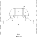
図1に示すように、従来の製造技術を実行する際、ゲート電極11は典型的に、ゲート絶縁層12(例えばゲート酸化物層)を半導体基板10とこのゲート電極11との間に挟んだ状態で、半導体基板10上に形成される。
その後、浅いソース/ドレイン拡張部13を注入すべく、イオン注入が実行される。
その後、例えば50Åから200Åの厚みで、酸化物ライナー14が、ゲート電極11の側面および基板10の上表面上に形成される。この酸化物ライナー14は、その後、側壁スペーサ15(典型的に窒化ケイ素からなる)を形成するために行われるエッチングの間、基板の表面を保護するために形成される。
参照符号14は、典型的に側壁スペーサ16を形成した後に注入される、適度にまたは高濃度にドープされた(heavy doped)ソース/ドレイン領域を示す。
As shown in FIG. 1, when performing a conventional manufacturing technique, the
Thereafter, ion implantation is performed to implant the shallow source /
Thereafter, an
図1に示される構造を形成する際に使用するような従来の半導体製造技術を実行する際には、以下のような不都合が生じる。
例えば、典型的に、約700℃以上の温度で行われる低圧の化学蒸着によって、シリコン酸化物ライナー15がたい積される間のような、高温処理の間に、ソース/ドレイン拡張部13に注入されたP型不純物(P-type impurities)(例えばホウ素(B)およびホウ素二弗化物(BF2)の不純物)のようなドーパント不純物は、酸化物ライナー15に拡散し分離する。
このような外方拡散およびドーパントの損失を防ぐため、より低い温度である400℃のCVDライナー酸化物を使用することができる。
しかしながらドーパントの損失は、5秒から10秒の間は100℃よりも高い温度である高温活性化中に生じる。
このようなソース/ドレイン拡張部からの拡散損失は、例えばソース/ドレイン拡張部の抵抗を増加させ、明らかに不利である。
この問題を解決する先の試みは、ドーパント拡散損失を補うために、必要とされる注入薬量よりも高い注入薬量で、ドーパント不純物(例えば、BまたはBF2)をイオン注入することを含む。
しかしながらこのアプローチは、不都合なことに、より深い接合深さ(Xj)を生じることとなる。この深い接合深さは、小型化に向けての流れと矛盾する。
The following inconveniences arise when performing conventional semiconductor manufacturing techniques such as those used in forming the structure shown in FIG.
For example, the source /
To prevent such out-diffusion and dopant loss, a lower temperature, 400 ° C. CVD liner oxide, can be used.
However, loss of dopant occurs during high temperature activation, which is a temperature higher than 100 ° C. for 5 to 10 seconds.
Such diffusion loss from the source / drain extension, for example, increases the resistance of the source / drain extension, which is clearly disadvantageous.
Previous attempts to solve this problem include ion implantation of dopant impurities (eg, B or BF 2 ) at higher implant doses than required to compensate for dopant diffusion losses. .
However, this approach unfortunately results in a deeper junction depth (X j ). This deep junction depth contradicts the trend toward miniaturization.
本発明の利点は、改善された性能を備えたトランジスタを有する高密度半導体デバイスを製造する方法である。 An advantage of the present invention is a method of manufacturing a high density semiconductor device having transistors with improved performance.
本発明のさらなる利点および他の構造は、以下の詳細な説明で記載される。そして、その一部は、以下の検討に基づいて、当業者に明白になるであろう。または本発明を実行することによって認識できる。
本発明の効果は、添付された請求項で特に指摘されるように、理解され、達成される。
Further advantages and other structures of the present invention are described in the detailed description below. Some of them will be apparent to those skilled in the art based on the following discussion. Or it can be recognized by carrying out the present invention.
The advantages of the invention will be realized and attained as particularly pointed out in the appended claims.
本発明の態様によれば、以下の半導体デバイスを製造する方法によって、前述した利点およびその他の利点の一部を達成することができる。この方法は、基板の上表面上に、側面を有するゲート電極をこのゲート電極と基板との間にゲート絶縁層を挟んだ状態で形成するステップと、浅いソース/ドレイン拡張部を形成すべく、前記ゲート電極をマスクとして使用して、ドーパントを前記基板にイオン注入するステップと、ゲート電極の側面および前記基板の上表面上に、酸化物ライナーを形成するステップと、前記酸化物ライナーに前記ドーパントをイオン注入するステップと、を含む。 In accordance with aspects of the present invention, the above-described advantages and some of the other advantages can be achieved by the following method of manufacturing a semiconductor device. The method includes: forming a gate electrode having a side surface on an upper surface of the substrate with a gate insulating layer sandwiched between the gate electrode and the substrate; and forming a shallow source / drain extension. Ion implanting dopant into the substrate using the gate electrode as a mask; forming an oxide liner on the side of the gate electrode and on the upper surface of the substrate; and the dopant in the oxide liner Ion implanting.
本発明の実施形態は、第1不純物濃度を有する浅いソース/ドレイン領域を形成すべく、前記基板中にホウ素(B)またはホウ素二弗化物(BF2)をイオン注入するステップと、前記ゲート電極の前記上表面および側面および前記基板の上表面上に、共形な酸化物ライナーをたい積するステップと、前記ソース/ドレイン拡張部中の不純物濃度と実質的に同じ濃度(例えば、約1×1020から約6×1020原子/cm3の濃度)で、前記酸化物ライナーにBまたはBF2をイオン注入するステップと、窒化ケイ素またはシリコン酸化窒化物のようなスペーサ層をたい積するステップと、側壁スペーサを形成すべく、エッチングするステップと、を含む。
その後、前記ゲート電極の上表面上にあるシリコン酸化物ライナーの部分は、除去される。
前記ゲート電極の上表面から前記酸化物ライナーの部分を除去する前または後のいずれかにおいて、比較的深い、適度なまたは高濃度のソース/ドレイン注入領域を形成すべく、イオン注入が実行される。
それから、活性アニーリングが実行される。
An embodiment of the present invention includes implanting boron (B) or boron difluoride (BF 2 ) into the substrate to form a shallow source / drain region having a first impurity concentration, and the gate electrode. Depositing a conformal oxide liner on the top and side surfaces of the substrate and on the top surface of the substrate, and substantially the same concentration as the impurity concentration in the source / drain extension (eg, about 1 × 10 Ion implanting B or BF 2 into the oxide liner at a concentration of 20 to about 6 × 10 20 atoms / cm 3 , and depositing a spacer layer such as silicon nitride or silicon oxynitride; Etching to form sidewall spacers.
Thereafter, the portion of the silicon oxide liner on the upper surface of the gate electrode is removed.
Either before or after removing the portion of the oxide liner from the upper surface of the gate electrode, ion implantation is performed to form a relatively deep, moderate or high concentration source / drain implant region. .
Then, active annealing is performed.
本発明のさらなる利点および態様は、以下の説明から当業者に容易に明白になるであろう。以下の記載では、本発明の好適な実施形態のみを本発明を実行するのに最適な実施形態の単なる一例として示し、説明する。
理解されるように、本発明は、その他の異なる実施形態とすることができ、またその各細部は、本発明の範囲内で、複数の観点において様々な修正を加えることができる。
従って、図面および詳細な説明は、本質的に単なる例であり、これに制限されない。
Additional advantages and aspects of the present invention will be readily apparent to those skilled in the art from the following description. In the following description, only preferred embodiments of the invention are shown and described as merely exemplary of the best embodiments for carrying out the invention.
As will be appreciated, the invention is capable of other and different embodiments, and its details are capable of various modifications in various respects, within the scope of the invention.
Accordingly, the drawings and detailed description are merely examples in nature and are not limiting.
図2から図4、図5から図8において、同様の構造または要素は、同様の参照符号によって示される。
本発明は、高密度で小型化された、信頼性の高い半導体デバイスに対する継続的な要求に向けられる。
本発明は、浅いソース/ドレイン拡張部から酸化物ライナー中への不純物の外方拡散に対するバリアを意図的に生成することによって、増強されたトランジスタ性能を備える半導体デバイスおよびこの半導体デバイスを実現する方法を提供する。
本発明の実施形態は、酸化物ライナーに不純物をイオン注入することによって、この目的を達成する。
したがって、本発明は、約200Åから約300Åの浅い接合深さ(Xj)を維持する一方で、P型不純物(例えば、BまたはBF2)のような不純物の外方拡散をなくすか著しく減少させる方法を提供する。
2 to 4 and 5 to 8, like structures or elements are indicated by like reference numerals.
The present invention is directed to the continuing need for high density, miniaturized, and reliable semiconductor devices.
The present invention relates to a semiconductor device with enhanced transistor performance by deliberately creating a barrier against outdiffusion of impurities from a shallow source / drain extension into an oxide liner, and a method for realizing the semiconductor device. I will provide a.
Embodiments of the present invention accomplish this goal by ion implanting impurities into the oxide liner.
Accordingly, the present invention eliminates or significantly reduces the outdiffusion of impurities such as P-type impurities (eg, B or BF 2 ) while maintaining a shallow junction depth (Xj) of about 200 to about 300 mm. Provide a method.
本発明の実施形態は、半導体基板上に、ゲート絶縁層をこの半導体基板とゲート電極との間に挟んだ状態でゲート電極を形成するステップと、浅いソース/ドレイン領域を形成すべく、マスクとして前記ゲート電極を使用して、基板中にBF2のようなドーパント不純物をイオン注入するステップと、を含む。
このようなイオン注入は、約5×10¹⁴ から約2×10¹⁵イオン/cm2の注入量および約1から約3KeVの注入エネルギー(典型的に、約1×1020から約6×1020原子/cm3の不純物濃度になる)で、BF2をイオン注入することによるような、従来の方式で行うことができる。
Embodiments of the present invention include a step of forming a gate electrode on a semiconductor substrate with a gate insulating layer sandwiched between the semiconductor substrate and the gate electrode, and a mask for forming a shallow source / drain region. Ion implanting a dopant impurity such as BF 2 into the substrate using the gate electrode.
Such ion implantation may include an implantation dose of about 5 × 10 14 to about 2 × 10 15 ions / cm 2 and an implantation energy of about 1 to about 3 KeV (typically about 1 × 10 20 to about 6 × 10 20 It can be done in a conventional manner, such as by ion implantation of BF 2 at an impurity concentration of atoms / cm 3 .
その後、シリコン酸化物ライナーは、例えば約50Åから200Åの厚みで、ゲート電極の上表面および側面と基板の上表面にたい積される。
その後、浅いソース/ドレイン拡張部を形成するのに使用される条件と実質的に同じ条件下で酸化物ライナーにBF2不純物を注入すべく、例えば約5×1014 から約2×10¹⁵イオン/cm2の注入エネルギーおよび約1から約3KeVの注入エネルギー(これにより、約1×1020から約6×1020原子/cm3の、酸化物ライナーにおける不純物濃度を形成する。)で、イオン注入が実行される。
Thereafter, a silicon oxide liner is deposited on the top and side surfaces of the gate electrode and the top surface of the substrate, for example with a thickness of about 50 to 200 inches.
Thereafter, for example, about 5 × 10 14 to about 2 × 10 15 ions are implanted to implant BF 2 impurities into the oxide liner under substantially the same conditions used to form the shallow source / drain extension. Ions with an implantation energy of / cm 2 and an implantation energy of about 1 to about 3 KeV (this forms an impurity concentration in the oxide liner of about 1 × 10 20 to about 6 × 10 20 atoms / cm 3 ). An injection is performed.
その後、例えば約600Åから約1200Åの厚みで、窒化ケイ素またはシリコン酸窒化物(silicon oxynitride)のようなスペーサ層がたい積されてもよい。
その後、側壁スペーサを形成すべく、異方性エッチングが実行される。
その後、比較的深い、適度なまたは高濃度のソース/ドレイン注入領域を形成すべく、BF2のイオン注入が実行される。
例えばフッ化水素酸を用いて適度なまたは高濃度のソース/ドレイン注入領域を形成すべく、イオン注入が実行される前または後のいずれかにおいて、ゲート電極の上表面上の酸化シリコンライナーの部分を、除去することができる。
その後、活性化アニーリングが実行されてもよい。
例えばスペーサ層をたい積し、活性化アニーリングする間のような、後の処理の間、拡散バリアを生成するためにシリコン酸化物ライナーにドーパント不純物を意図的に注入することは、浅いソース/ドレイン領域からの不純物の外方拡散を防ぐか、著しく減少させる。
Thereafter, a spacer layer such as silicon nitride or silicon oxynitride may be deposited, for example with a thickness of about 600 to about 1200.
Thereafter, anisotropic etching is performed to form sidewall spacers.
Thereafter, BF 2 ion implantation is performed to form a relatively deep, moderate or high concentration source / drain implantation region.
A portion of the silicon oxide liner on the upper surface of the gate electrode either before or after ion implantation is performed to form a moderate or highly concentrated source / drain implant region using, for example, hydrofluoric acid. Can be removed.
Thereafter, activation annealing may be performed.
Intentionally implanting dopant impurities into the silicon oxide liner to create a diffusion barrier during subsequent processing, such as during deposition of a spacer layer and activation annealing, is a shallow source / drain region. Prevents or significantly reduces the out-diffusion of impurities from.
本発明の実施形態は、図2ないし図4において概略的に示され、同様の要素または構造は、同様の参照符号および数字によって示される。
図2において、典型的にドープされた多結晶のゲート電極21は、典型的に単結晶のシリコンである基板20上、半導体基板上に形成されたエピタキシャル層またはウェル領域上に、形成される。
マスクとしてゲート電極21を使用する際、浅いソース/ドレイン拡張部23を形成する不純物は、BF2のような、基板20に注入されるイオンである。
その後、図3に示すように、例えば約50Åから約200Åのような厚みで、ゲート電極21の側面の上側面上、および基板20の上表面上に、シリコン酸化物ライナー30がたい積される。
その後、図3の矢印31によって示されるように、酸化物ライナー31にBF2を注入すべく、浅いソース/ドレイン拡張部23に注入されるのと実質的に同じ濃度でイオン注入が実行される。
これにより、浅いソース/ドレイン拡張部23からBF2原子が外方拡散しないようにするバリアを生成する。
Embodiments of the present invention are schematically illustrated in FIGS. 2-4, wherein like elements or structures are indicated by like reference numerals and numbers.
In FIG. 2, a typically doped
When using the
Thereafter, as shown in FIG. 3, a
Thereafter, as shown by
This creates a barrier that prevents BF 2 atoms from diffusing out of the shallow source /
その後、図4に示すように、スペーサ材料の層がたい積され、側壁スペーサ40を形成すべく、典型的に基板表面の約600Åから約1200Åの厚みにおいて、異方性エッチングが実行される。
シリコン酸化層30は、側壁スペーサ40を形成するためのエッチングの間、エッチング停止層の役割を果たし、これにより、基板20に対するダメージが回避される。
後の処理は、ゲート電極21および基板20の上表面から、例えばフッ化水素酸を使用して、シリコン酸化物ライナー30を除去することを含む。
イオン注入は、ゲート電極21および基板の上表面からシリコン酸化物層40のシリコンの部分を除去する前か後に、深い、適度なまたは高濃度にドープされたソース/ドレイン領域41を形成すべく、実行される。その結果、図4に概略的に示された構造が生成される。
Thereafter, as shown in FIG. 4, a layer of spacer material is deposited and anisotropic etching is performed, typically at a thickness of about 600 to about 1200 mm of the substrate surface, to form
The
Subsequent processing includes removing the
Ion implantation is performed to form deep, moderately or heavily doped source /
他の発明の態様は、SOI(silicon-on-insulative)構造の2重(dual)埋込酸化膜(BOX)中のソース/ドレイン領域の厚みの選択的な最適化を可能にする方法を含む。
このような発明の方法は、図5ないし図8において、概略的に示され、同様の構造または要素は、同様の参照符号によって示される。
図5では、2重BOX構造は、シリコン50、BOX51、シリコン層52、BOX53およびシリコン層54から形成された基板を含む。
ゲート電極55は、ゲート絶縁層56をこのゲート電極55と基板との間に挟んで2重BOX上に形成される。
Another aspect of the invention includes a method that allows selective optimization of the thickness of the source / drain regions in a dual buried oxide (BOX) with a silicon-on-insulative (SOI) structure. .
Such inventive methods are schematically illustrated in FIGS. 5-8, wherein like structures or elements are indicated by like reference numerals.
In FIG. 5, the double BOX structure includes a substrate formed from
The
その後、図6に示すように、フォトレジスト・マスク60が、この構造のソース側の上に形成される。
それから、図7に示すように、ドレイン側から上部のシリコン層54および上部のBOX層53を除去すべく、エッチングが実行される。
続いて、図8に示すように、より下側のシリコン層52から特定の方向に(エピタクシーに)54Aを成長させる。
このように、より深いドレイン領域54Aが、ソース領域54Bと別個に形成することができる。
Thereafter, as shown in FIG. 6, a
Then, as shown in FIG. 7, etching is performed to remove the
Subsequently, as shown in FIG. 8, a 54A is grown in a specific direction (epitaxy) from the
Thus, the
本発明は、トランジスタの性能を改善し、浅い接合深さ(Xj)、例えば約200Åから約300Åの深さを示す、半導体素子の製造を可能にする。
同じタイプの不純物が、浅いソース/ドレイン拡張部における濃度と同じ濃度で、酸化物ライナーに注入される。これにより、
浅いソース/ドレイン領域からの不純物の外方拡散を防止または実質的に減少し、これに伴いソース/ドレイン拡張部の抵抗が改良され、小型化されると共にトランジスタ性能が著しく改良される。
The present invention improves transistor performance and enables the fabrication of semiconductor devices that exhibit shallow junction depth (Xj), for example, about 200 to about 300 inches.
The same type of impurity is implanted into the oxide liner at the same concentration as in the shallow source / drain extension. This
Preventing or substantially reducing the out-diffusion of impurities from the shallow source / drain regions, resulting in improved resistance of the source / drain extension, miniaturization and significantly improved transistor performance.
本発明は、様々なタイプの半導体デバイスの製造において、産業上の利用可能性を有する。
本発明は、特に、約0.12ミクロンのデザインルールで高密度半導体素子を製造する際に適用することができる。
The present invention has industrial applicability in the manufacture of various types of semiconductor devices.
The present invention is particularly applicable when manufacturing high density semiconductor devices with a design rule of about 0.12 microns.
以上の記載において、本発明についてのさらなる理解を提供すべく、特定の材料、構造、薬品、プロセス等のように多数の特定の詳細を記載した。しかしながら、本発明は特別に記載された詳細によらずに実行することができる。
その他、既知の処理および材料は、本発明を不必要に不明瞭にしないため、詳細には記載されていない。
In the foregoing description, numerous specific details have been set forth, such as specific materials, structures, agents, processes, etc., in order to provide a further understanding of the invention. However, the invention can be practiced without the details specifically described.
In other instances, well-known processes and materials have not been described in detail in order not to unnecessarily obscure the present invention.
本発明の好ましい実施形態のみであるが、その多様性のうちのいくつかの例が、本発明において示されると共に、記載される。
本発明は、様々な他の組合わせおよび環境において使用できると共に、ここに記載されるような本発明の概念の範囲内の変形または修正することができるものとして理解される。
Although only preferred embodiments of the invention, some examples of its variety are shown and described in the present invention.
It is understood that the present invention can be used in various other combinations and environments and can be varied or modified within the scope of the inventive concept as described herein.
Claims (11)
浅いソース/ドレイン拡張部を形成すべく、前記ゲート電極をマスクとして使用して、ドーパントを前記基板にイオン注入するステップと、
前記ゲート電極の側面および前記基板の上表面上に、酸化物ライナーを形成するステップと、
前記酸化物ライナーに、前記浅いソース/ドレイン拡張部の不純物濃度と同じ不純物濃度で、前記ドーパントをイオン注入するステップと、
を含む、半導体デバイスを製造する方法。Forming a gate electrode having a side surface on an upper surface of the substrate with a gate insulating layer sandwiched between the gate electrode and the substrate;
Implanting dopant into the substrate using the gate electrode as a mask to form a shallow source / drain extension;
Forming an oxide liner on a side surface of the gate electrode and an upper surface of the substrate;
Ion-implanting the dopant into the oxide liner at the same impurity concentration as that of the shallow source / drain extension ;
A method of manufacturing a semiconductor device, comprising:
前記酸化物ライナー上に側壁スペーサを形成すべく、エッチングするステップと、
ドープされたインプラントを形成すべく、前記基板にドーパントをイオン注入するステップと、
活性化アニーリングするステップと、をさらに含む、請求項1または2記載の方法。Depositing a layer of spacer material on the oxide liner;
Etching to form sidewall spacers on the oxide liner;
Ion implanting a dopant into the substrate to form a doped implant ;
The method of claim 1, further comprising the step of activation annealing.
窒化ケイ素またはシリコン酸化窒化物を含む前記スペーサ層を形成するステップと、を含む、請求項3記載の方法。Forming the oxide liner comprising silicon oxide;
Forming the spacer layer comprising silicon nitride or silicon oxynitride.
前記第1不純物濃度と同じ濃度で、前記酸化物ライナーに前記ドーパントをイオン注入するステップと、を含む、請求項1ないし6のいずれかの項記載の方法。Ion implanting the dopant into the substrate to form the shallow source / drain extension at a first impurity concentration;
The method according to claim 1 , further comprising: ion-implanting the dopant into the oxide liner at the same concentration as the first impurity concentration.
Applications Claiming Priority (2)
| Application Number | Priority Date | Filing Date | Title |
|---|---|---|---|
| US10/105,522 US6583016B1 (en) | 2002-03-26 | 2002-03-26 | Doped spacer liner for improved transistor performance |
| PCT/US2003/007559 WO2003083929A1 (en) | 2002-03-26 | 2003-03-13 | Ion implantation of silicon oxid liner to prevent dopant out-diffusion from so urce/drain extensions |
Publications (3)
| Publication Number | Publication Date |
|---|---|
| JP2005522033A JP2005522033A (en) | 2005-07-21 |
| JP2005522033A5 JP2005522033A5 (en) | 2006-04-27 |
| JP4514023B2 true JP4514023B2 (en) | 2010-07-28 |
Family
ID=22306307
Family Applications (1)
| Application Number | Title | Priority Date | Filing Date |
|---|---|---|---|
| JP2003581249A Expired - Fee Related JP4514023B2 (en) | 2002-03-26 | 2003-03-13 | Silicon oxide liner ion implantation to prevent dopants from diffusing out of source / drain extensions |
Country Status (8)
| Country | Link |
|---|---|
| US (1) | US6583016B1 (en) |
| EP (1) | EP1488453A1 (en) |
| JP (1) | JP4514023B2 (en) |
| KR (1) | KR100948939B1 (en) |
| CN (1) | CN100355046C (en) |
| AU (1) | AU2003220198A1 (en) |
| TW (1) | TWI270933B (en) |
| WO (1) | WO2003083929A1 (en) |
Families Citing this family (13)
| Publication number | Priority date | Publication date | Assignee | Title |
|---|---|---|---|---|
| US6777298B2 (en) * | 2002-06-14 | 2004-08-17 | International Business Machines Corporation | Elevated source drain disposable spacer CMOS |
| JP4112330B2 (en) * | 2002-10-02 | 2008-07-02 | 富士通株式会社 | Manufacturing method of semiconductor device |
| JP2004363443A (en) * | 2003-06-06 | 2004-12-24 | Toshiba Corp | Non-volatile semiconductor storage device and its manufacturing method |
| US6812105B1 (en) * | 2003-07-16 | 2004-11-02 | International Business Machines Corporation | Ultra-thin channel device with raised source and drain and solid source extension doping |
| CN1296987C (en) * | 2003-09-23 | 2007-01-24 | 茂德科技股份有限公司 | Mfg method of contact hole and mfg method of semiconductor element |
| JP2007525813A (en) * | 2003-12-04 | 2007-09-06 | インターナショナル・ビジネス・マシーンズ・コーポレーション | Method for forming a non-amorphous ultra-thin semiconductor device using a sacrificial implant layer |
| US20070029608A1 (en) * | 2005-08-08 | 2007-02-08 | Taiwan Semiconductor Manufacturing Company, Ltd. | Offset spacers for CMOS transistors |
| KR100649311B1 (en) * | 2005-12-15 | 2006-11-24 | 동부일렉트로닉스 주식회사 | Method for forming compressive channel of pmos device using gate spacer, and pmos device manufactured by the same |
| JP6087672B2 (en) * | 2012-03-16 | 2017-03-01 | 株式会社半導体エネルギー研究所 | Semiconductor device |
| US9093554B2 (en) * | 2012-05-14 | 2015-07-28 | Globalfoundries Inc. | Methods of forming semiconductor devices with embedded semiconductor material as source/drain regions using a reduced number of spacers |
| US10141417B2 (en) * | 2015-10-20 | 2018-11-27 | Taiwan Semiconductor Manufacturing Company, Ltd. | Gate structure, semiconductor device and the method of forming semiconductor device |
| US10770354B2 (en) * | 2017-11-15 | 2020-09-08 | Taiwan Semiconductor Manufacturing Co., Ltd. | Method of forming integrated circuit with low-k sidewall spacers for gate stacks |
| CN110265481B (en) * | 2018-08-10 | 2023-01-17 | 友达光电股份有限公司 | Transistor arrangement |
Family Cites Families (22)
| Publication number | Priority date | Publication date | Assignee | Title |
|---|---|---|---|---|
| US165659A (en) * | 1875-07-20 | Improvement in registering board-rules | ||
| US619098A (en) * | 1899-02-07 | Steam-boiler | ||
| JPH0834313B2 (en) * | 1989-10-09 | 1996-03-29 | 株式会社東芝 | Semiconductor device and manufacturing method thereof |
| KR950000141B1 (en) * | 1990-04-03 | 1995-01-10 | 미쓰비시 뎅끼 가부시끼가이샤 | Semiconductor device & manufacturing method thereof |
| JPH05267327A (en) * | 1992-03-18 | 1993-10-15 | Fujitsu Ltd | Misfet and its manufacture |
| JPH0823031A (en) * | 1994-07-05 | 1996-01-23 | Oki Electric Ind Co Ltd | Semiconductor device and manufacture thereof |
| JPH0897173A (en) * | 1994-09-22 | 1996-04-12 | Sony Corp | Manufacture of semiconductor device |
| JPH08288504A (en) * | 1995-04-14 | 1996-11-01 | Sony Corp | Method of semiconductor device |
| CN1057867C (en) * | 1995-12-20 | 2000-10-25 | 台湾茂矽电子股份有限公司 | Method for making semiconductor device of channel area compensation formed by phosphorus injection |
| US5756383A (en) * | 1996-12-23 | 1998-05-26 | Advanced Micro Devices | Method of manufacturing an active region of a semiconductor by diffusing a counterdopant out of a sidewall spacer |
| US6117719A (en) * | 1997-12-18 | 2000-09-12 | Advanced Micro Devices, Inc. | Oxide spacers as solid sources for gallium dopant introduction |
| JPH11238882A (en) * | 1998-02-23 | 1999-08-31 | Sony Corp | Manufacture of semiconductor device |
| JP3425079B2 (en) * | 1998-04-24 | 2003-07-07 | 三菱電機株式会社 | Method for manufacturing semiconductor device |
| US6162692A (en) * | 1998-06-26 | 2000-12-19 | Advanced Micro Devices, Inc. | Integration of a diffusion barrier layer and a counter dopant region to maintain the dopant level within the junctions of a transistor |
| US6156598A (en) * | 1999-12-13 | 2000-12-05 | Chartered Semiconductor Manufacturing Ltd. | Method for forming a lightly doped source and drain structure using an L-shaped spacer |
| US6190982B1 (en) * | 2000-01-28 | 2001-02-20 | United Microelectronics Corp. | Method of fabricating a MOS transistor on a semiconductor wafer |
| US6346468B1 (en) * | 2000-02-11 | 2002-02-12 | Chartered Semiconductor Manufacturing Ltd. | Method for forming an L-shaped spacer using a disposable polysilicon spacer |
| US6235600B1 (en) * | 2000-03-20 | 2001-05-22 | Taiwan Semiconductor Manufacturing Company | Method for improving hot carrier lifetime via a nitrogen implantation procedure performed before or after a teos liner deposition |
| JP2001291861A (en) * | 2000-04-05 | 2001-10-19 | Nec Corp | Mos transistor and method for manufacturing the same |
| JP2002076336A (en) * | 2000-09-01 | 2002-03-15 | Mitsubishi Electric Corp | Semiconductor device and soi substrate |
| JP2005517285A (en) * | 2001-12-19 | 2005-06-09 | アドバンスト・マイクロ・ディバイシズ・インコーポレイテッド | Semiconductor device including thin oxide liner and method of manufacturing the same |
| JP3966243B2 (en) * | 2003-07-09 | 2007-08-29 | トヨタ自動車株式会社 | Internal combustion engine |
-
2002
- 2002-03-26 US US10/105,522 patent/US6583016B1/en not_active Expired - Lifetime
-
2003
- 2003-03-13 KR KR1020047015039A patent/KR100948939B1/en not_active IP Right Cessation
- 2003-03-13 AU AU2003220198A patent/AU2003220198A1/en not_active Abandoned
- 2003-03-13 WO PCT/US2003/007559 patent/WO2003083929A1/en active Application Filing
- 2003-03-13 EP EP03716494A patent/EP1488453A1/en not_active Withdrawn
- 2003-03-13 JP JP2003581249A patent/JP4514023B2/en not_active Expired - Fee Related
- 2003-03-13 CN CNB038067633A patent/CN100355046C/en not_active Expired - Lifetime
- 2003-03-21 TW TW092106269A patent/TWI270933B/en not_active IP Right Cessation
Also Published As
| Publication number | Publication date |
|---|---|
| TWI270933B (en) | 2007-01-11 |
| KR100948939B1 (en) | 2010-03-23 |
| TW200305940A (en) | 2003-11-01 |
| KR20040093183A (en) | 2004-11-04 |
| AU2003220198A1 (en) | 2003-10-13 |
| CN100355046C (en) | 2007-12-12 |
| US6583016B1 (en) | 2003-06-24 |
| EP1488453A1 (en) | 2004-12-22 |
| CN1643672A (en) | 2005-07-20 |
| JP2005522033A (en) | 2005-07-21 |
| WO2003083929A1 (en) | 2003-10-09 |
Similar Documents
| Publication | Publication Date | Title |
|---|---|---|
| US6707062B2 (en) | Transistor in a semiconductor device with an elevated channel and a source drain | |
| US5766969A (en) | Multiple spacer formation/removal technique for forming a graded junction | |
| US7553717B2 (en) | Recess etch for epitaxial SiGe | |
| US6917085B2 (en) | Semiconductor transistor using L-shaped spacer | |
| US7701010B2 (en) | Method of fabricating transistor including buried insulating layer and transistor fabricated using the same | |
| US6184097B1 (en) | Process for forming ultra-shallow source/drain extensions | |
| US5585295A (en) | Method for forming inverse-T gate lightly-doped drain (ITLDD) device | |
| US6924180B2 (en) | Method of forming a pocket implant region after formation of composite insulator spacers | |
| US20060154411A1 (en) | CMOS transistors and methods of forming same | |
| JP3821707B2 (en) | Manufacturing method of semiconductor device | |
| US7098099B1 (en) | Semiconductor device having optimized shallow junction geometries and method for fabrication thereof | |
| JP4514023B2 (en) | Silicon oxide liner ion implantation to prevent dopants from diffusing out of source / drain extensions | |
| US20060001105A1 (en) | Semiconductor device having optimized shallow junction geometries and method for fabrication thereof | |
| US20020090787A1 (en) | Self-aligned elevated transistor | |
| CN116504718B (en) | Manufacturing method of semiconductor structure | |
| US6391733B1 (en) | Method of doping semiconductor devices through a layer of dielectric material | |
| US8395221B2 (en) | Depletion-free MOS using atomic-layer doping | |
| US6069046A (en) | Transistor fabrication employing implantation of dopant into junctions without subjecting sidewall surfaces of a gate conductor to ion bombardment | |
| US20100032813A1 (en) | Ic formed with densified chemical oxide layer | |
| JP3166911B2 (en) | Method for manufacturing semiconductor device | |
| US20050026406A1 (en) | Method for fabricating poly patterns | |
| US20050208726A1 (en) | Spacer approach for CMOS devices | |
| CN113394101A (en) | NMOS device manufacturing method for improving stress film coverage uniformity and NMOS device | |
| JPH11154650A (en) | Manufacture of semiconductor device | |
| KR20050026147A (en) | Method of manufacturing semiconductor device |
Legal Events
| Date | Code | Title | Description |
|---|---|---|---|
| A521 | Written amendment |
Free format text: JAPANESE INTERMEDIATE CODE: A523 Effective date: 20060310 |
|
| A621 | Written request for application examination |
Free format text: JAPANESE INTERMEDIATE CODE: A621 Effective date: 20060310 |
|
| A977 | Report on retrieval |
Free format text: JAPANESE INTERMEDIATE CODE: A971007 Effective date: 20080526 |
|
| A131 | Notification of reasons for refusal |
Free format text: JAPANESE INTERMEDIATE CODE: A131 Effective date: 20091124 |
|
| A601 | Written request for extension of time |
Free format text: JAPANESE INTERMEDIATE CODE: A601 Effective date: 20100224 |
|
| A602 | Written permission of extension of time |
Free format text: JAPANESE INTERMEDIATE CODE: A602 Effective date: 20100303 |
|
| A521 | Written amendment |
Free format text: JAPANESE INTERMEDIATE CODE: A523 Effective date: 20100324 |
|
| TRDD | Decision of grant or rejection written | ||
| A01 | Written decision to grant a patent or to grant a registration (utility model) |
Free format text: JAPANESE INTERMEDIATE CODE: A01 Effective date: 20100420 |
|
| A01 | Written decision to grant a patent or to grant a registration (utility model) |
Free format text: JAPANESE INTERMEDIATE CODE: A01 |
|
| RD03 | Notification of appointment of power of attorney |
Free format text: JAPANESE INTERMEDIATE CODE: A7423 Effective date: 20100421 |
|
| A61 | First payment of annual fees (during grant procedure) |
Free format text: JAPANESE INTERMEDIATE CODE: A61 Effective date: 20100506 |
|
| R150 | Certificate of patent or registration of utility model |
Free format text: JAPANESE INTERMEDIATE CODE: R150 |
|
| FPAY | Renewal fee payment (event date is renewal date of database) |
Free format text: PAYMENT UNTIL: 20130521 Year of fee payment: 3 |
|
| RD05 | Notification of revocation of power of attorney |
Free format text: JAPANESE INTERMEDIATE CODE: A7425 Effective date: 20100902 |
|
| A072 | Dismissal of procedure [no reply to invitation to correct request for examination] |
Free format text: JAPANESE INTERMEDIATE CODE: A072 Effective date: 20101222 |
|
| LAPS | Cancellation because of no payment of annual fees |