KR101160836B1 - Display device and shift register therefor - Google Patents
Display device and shift register therefor Download PDFInfo
- Publication number
- KR101160836B1 KR101160836B1 KR1020050089827A KR20050089827A KR101160836B1 KR 101160836 B1 KR101160836 B1 KR 101160836B1 KR 1020050089827 A KR1020050089827 A KR 1020050089827A KR 20050089827 A KR20050089827 A KR 20050089827A KR 101160836 B1 KR101160836 B1 KR 101160836B1
- Authority
- KR
- South Korea
- Prior art keywords
- output
- voltage
- signal
- switching
- transistor
- Prior art date
Links
Images


Classifications
-
- G—PHYSICS
- G09—EDUCATION; CRYPTOGRAPHY; DISPLAY; ADVERTISING; SEALS
- G09G—ARRANGEMENTS OR CIRCUITS FOR CONTROL OF INDICATING DEVICES USING STATIC MEANS TO PRESENT VARIABLE INFORMATION
- G09G3/00—Control arrangements or circuits, of interest only in connection with visual indicators other than cathode-ray tubes
- G09G3/20—Control arrangements or circuits, of interest only in connection with visual indicators other than cathode-ray tubes for presentation of an assembly of a number of characters, e.g. a page, by composing the assembly by combination of individual elements arranged in a matrix no fixed position being assigned to or needed to be assigned to the individual characters or partial characters
- G09G3/34—Control arrangements or circuits, of interest only in connection with visual indicators other than cathode-ray tubes for presentation of an assembly of a number of characters, e.g. a page, by composing the assembly by combination of individual elements arranged in a matrix no fixed position being assigned to or needed to be assigned to the individual characters or partial characters by control of light from an independent source
- G09G3/36—Control arrangements or circuits, of interest only in connection with visual indicators other than cathode-ray tubes for presentation of an assembly of a number of characters, e.g. a page, by composing the assembly by combination of individual elements arranged in a matrix no fixed position being assigned to or needed to be assigned to the individual characters or partial characters by control of light from an independent source using liquid crystals
- G09G3/3611—Control of matrices with row and column drivers
- G09G3/3674—Details of drivers for scan electrodes
- G09G3/3677—Details of drivers for scan electrodes suitable for active matrices only
-
- G—PHYSICS
- G11—INFORMATION STORAGE
- G11C—STATIC STORES
- G11C19/00—Digital stores in which the information is moved stepwise, e.g. shift registers
- G11C19/18—Digital stores in which the information is moved stepwise, e.g. shift registers using capacitors as main elements of the stages
- G11C19/182—Digital stores in which the information is moved stepwise, e.g. shift registers using capacitors as main elements of the stages in combination with semiconductor elements, e.g. bipolar transistors, diodes
- G11C19/184—Digital stores in which the information is moved stepwise, e.g. shift registers using capacitors as main elements of the stages in combination with semiconductor elements, e.g. bipolar transistors, diodes with field-effect transistors, e.g. MOS-FET
-
- G—PHYSICS
- G11—INFORMATION STORAGE
- G11C—STATIC STORES
- G11C19/00—Digital stores in which the information is moved stepwise, e.g. shift registers
- G11C19/28—Digital stores in which the information is moved stepwise, e.g. shift registers using semiconductor elements
-
- H—ELECTRICITY
- H03—ELECTRONIC CIRCUITRY
- H03K—PULSE TECHNIQUE
- H03K23/00—Pulse counters comprising counting chains; Frequency dividers comprising counting chains
-
- G—PHYSICS
- G09—EDUCATION; CRYPTOGRAPHY; DISPLAY; ADVERTISING; SEALS
- G09G—ARRANGEMENTS OR CIRCUITS FOR CONTROL OF INDICATING DEVICES USING STATIC MEANS TO PRESENT VARIABLE INFORMATION
- G09G2300/00—Aspects of the constitution of display devices
- G09G2300/04—Structural and physical details of display devices
- G09G2300/0439—Pixel structures
-
- G—PHYSICS
- G09—EDUCATION; CRYPTOGRAPHY; DISPLAY; ADVERTISING; SEALS
- G09G—ARRANGEMENTS OR CIRCUITS FOR CONTROL OF INDICATING DEVICES USING STATIC MEANS TO PRESENT VARIABLE INFORMATION
- G09G2310/00—Command of the display device
- G09G2310/02—Addressing, scanning or driving the display screen or processing steps related thereto
- G09G2310/0264—Details of driving circuits
- G09G2310/0281—Arrangement of scan or data electrode driver circuits at the periphery of a panel not inherent to a split matrix structure
-
- G—PHYSICS
- G09—EDUCATION; CRYPTOGRAPHY; DISPLAY; ADVERTISING; SEALS
- G09G—ARRANGEMENTS OR CIRCUITS FOR CONTROL OF INDICATING DEVICES USING STATIC MEANS TO PRESENT VARIABLE INFORMATION
- G09G2310/00—Command of the display device
- G09G2310/02—Addressing, scanning or driving the display screen or processing steps related thereto
- G09G2310/0264—Details of driving circuits
- G09G2310/0286—Details of a shift registers arranged for use in a driving circuit
Landscapes
- Engineering & Computer Science (AREA)
- Microelectronics & Electronic Packaging (AREA)
- Computer Hardware Design (AREA)
- Theoretical Computer Science (AREA)
- General Physics & Mathematics (AREA)
- Physics & Mathematics (AREA)
- Chemical & Material Sciences (AREA)
- Crystallography & Structural Chemistry (AREA)
- Power Engineering (AREA)
- Control Of Indicators Other Than Cathode Ray Tubes (AREA)
- Shift Register Type Memory (AREA)
- Liquid Crystal Display Device Control (AREA)
- Liquid Crystal (AREA)
Abstract
본 발명의 실시예에 따른 시프트 레지스터는 서로 연결되어 있으며 차례대로 출력 신호를 생성하는 복수의 스테이지를 포함하며, 상기 각 스테이지는 적어도 두 개의 게이트선과 각각 연결되어 박막 트랜지스터를 턴온시키는 제1 출력 전압을 상기 적어도 두 개의 게이트선에 번갈아 출력하는 복수의 출력단을 가진다.The shift register according to the embodiment of the present invention includes a plurality of stages connected to each other and sequentially generating an output signal, wherein each stage is connected to at least two gate lines to respectively turn on a first output voltage to turn on the thin film transistor. And a plurality of output terminals alternately outputting the at least two gate lines.
Description
도 1은 본 발명의 한 실시예에 따른 액정 표시 장치의 블록도이고,1 is a block diagram of a liquid crystal display according to an exemplary embodiment of the present invention.
도 2는 본 발명의 한 실시예에 따른 액정 표시 장치의 한 화소에 대한 등가 회로도이고,2 is an equivalent circuit diagram of one pixel of a liquid crystal display according to an exemplary embodiment of the present invention.
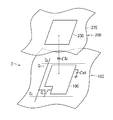
도 3은 도 1에 도시한 게이트 구동부를 나타낸 블록도의 한 예이며,3 is an example of a block diagram illustrating the gate driver illustrated in FIG. 1.
도 4는 도 3에 도시한 게이트 구동부의 한 스테이지의 회로도의 한 예이다.FIG. 4 is an example of a circuit diagram of one stage of the gate driver shown in FIG. 3.
본 발명은 시프트 레지스터 및 이를 포함하는 표시 장치에 관한 것이다.The present invention relates to a shift register and a display device including the same.
액정 표시 장치는 현재 가장 널리 사용되고 있는 평판 표시 장치 중 하나로서, 화소 전극과 공통 전극 등 전기장 생성 전극이 형성되어 있는 두 장의 표시판과 그 사이에 들어 있는 액정층을 포함한다. 액정 표시 장치는 전기장 생성 전극에 전압을 인가하여 액정층에 전기장을 생성하고, 이를 통하여 액정층의 액정 분자들의 배향을 결정하고 입사광의 편광을 제어함으로써 영상을 표시한다.The liquid crystal display is one of the most widely used flat panel display devices, and includes two display panels on which an electric field generating electrode such as a pixel electrode and a common electrode are formed, and a liquid crystal layer interposed therebetween. The liquid crystal display generates an electric field in the liquid crystal layer by applying a voltage to the field generating electrode, thereby determining an orientation of liquid crystal molecules in the liquid crystal layer and controlling the polarization of incident light to display an image.
액정 표시 장치를 비롯한 표시 장치는 또한 각 화소 전극에 연결되어 있는 스위칭 소자 및 스위칭 소자를 제어하여 화소 전극에 전압을 인가하기 위한 게이트선과 데이터선 등 다수의 신호선을 포함한다.A display device including a liquid crystal display device also includes a switching element connected to each pixel electrode and a plurality of signal lines such as a gate line and a data line for controlling a switching element and applying a voltage to the pixel electrode.
이러한 신호선은 별도로 마련된 구동 장치로부터 신호를 인가 받아, 스위칭 소자를 통하여 해당 화소에 해당 신호를 인가한다. 따라서 표시 장치를 구동하기 위해서는 구동 장치를 표시 장치에 연결하거나 표시 장치에 장착해야 한다. 그러나 이러한 구동 장치는 표시 장치를 제조할 때 높은 비용을 차지한다.The signal line receives a signal from a separately provided driving device and applies the signal to the pixel through a switching element. Therefore, in order to drive the display device, the driving device must be connected to or mounted on the display device. However, such a driving device takes a high cost when manufacturing a display device.
본 발명이 이루고자 하는 기술적 과제는 액정 표시 장치에 설치되는 구동부에 소비되는 비용을 감소시키는 것이다.An object of the present invention is to reduce the cost consumed in the driving unit installed in the liquid crystal display.
본 발명의 실시예에 따른 시프트 레지스터는 서로 연결되어 있으며 차례대로 출력 신호를 생성하는 복수의 스테이지를 포함하며, 상기 각 스테이지는 서로 교대로 제1 출력 전압을 출력하는 제1 및 제2 출력단을 가진다.The shift register according to the embodiment of the present invention includes a plurality of stages connected to each other and sequentially generating output signals, each stage having first and second output stages which alternately output a first output voltage. .
본 발명의 한 실시예에 따른 표시 장치는, 기판, 상기 기판 위에 형성되어 있는 복수의 게이트선, 상기 게이트선과 교차하는 복수의 데이터선, 상기 게이트선 및 상기 데이터선과 연결되어 있는 복수의 박막 트랜지스터, 상기 박막 트랜지스터와 연결되어 있고 행렬의 형태로 배열되어 있으며, 상기 게이트선에 평행한 제1변 및 상기 제1변보다 길이가 짧으며 상기 제1변과 이웃하는 제2변을 갖는 복수의 화소 전극, 그리고 상기 게이트선과 연결되어 있는 게이트 구동부를을 포함하며, 상기 게이트 구동부는 서로 연결되어 있으며 차례대로 출력 신호를 생성하는 복수의 스테이지를 포함하며, 상기 각 스테이지는 적어도 두 개의 게이트선과 각각 연결되어 상기 박막 트랜지스터를 턴온시키는 제1 출력 전압을 상기 적어도 두 개의 게이트선에 번갈아 출력하는 복수의 출력단을 가진다.According to an exemplary embodiment, a display device includes a substrate, a plurality of gate lines formed on the substrate, a plurality of data lines crossing the gate lines, a plurality of thin film transistors connected to the gate lines and the data lines, A plurality of pixel electrodes connected to the thin film transistors and arranged in a matrix form and having a first side parallel to the gate line and a length shorter than the first side and adjacent to the first side; And a gate driver connected to the gate line, wherein the gate driver includes a plurality of stages connected to each other and sequentially generating output signals, wherein each stage is connected to at least two gate lines, respectively. Alternately outputting a first output voltage for turning on the thin film transistor to the at least two gate lines It has a plurality of output terminals.
상기 각 스테이지는 출력 시작 신호 또는 전단 스테이지 중 하나의 출력 신호에 응답하여 상기 제1 출력 전압을 생성하고 후단 스테이지 중 어느 하나의 제1 출력 전압에 응답하여 상기 제1 출력 전압보다 크기가 작은 제2 출력 전압을 생성하는 출력 전압 생성부를 포함할 수 있다.Each of the stages generates a first output voltage in response to an output signal of one of an output start signal or a previous stage and a second smaller in magnitude than the first output voltage in response to a first output voltage of any one of a subsequent stage; It may include an output voltage generator for generating an output voltage.
상기 각 스테이지는 상기 제1 출력 전압과 상기 제2 출력 전압을 스위칭하여 상기 제1 출력단과 상기 제2 출력단으로 번갈아 바꾸어 출력하는 출력 스위칭부를 더 포함할 수 있다.Each stage may further include an output switching unit configured to switch the first output voltage and the second output voltage to alternately output the first output terminal and the second output terminal.
상기 출력 스위칭부는, 제1 스위칭 신호에 따라 상기 전압 생성부의 출력을 스위칭하는 제1 트랜지스터, 그리고 제2 스위칭 신호에 따라 상기 전압 생성부의 출력을 스위칭하는 제2 트랜지스터를 포함할 수 있다.The output switching unit may include a first transistor for switching the output of the voltage generator according to a first switching signal, and a second transistor for switching the output of the voltage generator according to a second switching signal.
상기 제1 스위칭 신호와 상기 제2 스위칭 신호의 위상은 서로 반대일 수 있다.Phases of the first switching signal and the second switching signal may be opposite to each other.
상기 출력 스위칭부는, 상기 제2 스위칭 신호에 따라 상기 제2 출력 전압을 상기 제1 출력 단자로 출력 또는 차단하는 제3 트랜지스터, 그리고 상기 제1 스위칭 신호에 따라 상기 제2 출력 전압을 상기 제2 출력 단자로 출력 또는 차단하는 제4 트랜지스터를 더 포함할 수 있다.The output switching unit may include a third transistor configured to output or block the second output voltage to the first output terminal according to the second switching signal, and the second output voltage to the second output voltage according to the first switching signal. The device may further include a fourth transistor outputting to or blocking the terminal.
상기 제1 및 제2 스위칭 신호는 반 프레임을 주기로 하여 반전될 수 있다.The first and second switching signals may be inverted every half frame.
열 방향으로 인접한 화소 전극은 서로 다른 데이터선과 연결되어 있을 수 있다.Pixel electrodes adjacent in the column direction may be connected to different data lines.
상기 게이트 구동부는 서로 다른 게이트선에 연결되어 있는 제1 및 제2 시프트 레지스터를 포함하며, 상기 제1 및 제2 시프트 레지스터 각각은 상기 스테이지를 포함할 수 있다.The gate driver may include first and second shift registers connected to different gate lines, and each of the first and second shift registers may include the stage.
그러면 첨부한 도면을 참고로 하여 본 발명의 실시예에 대하여 본 발명이 속하는 기술 분야에서 통상의 지식을 가진 자가 용이하게 실시할 수 있도록 상세히 설명한다. 그러나 본 발명은 여러 가지 상이한 형태로 구현될 수 있으며 여기에서 설명하는 실시예에 한정되지 않는다.DETAILED DESCRIPTION Hereinafter, exemplary embodiments of the present invention will be described in detail with reference to the accompanying drawings so that those skilled in the art may easily implement the present invention. The present invention may, however, be embodied in many different forms and should not be construed as limited to the embodiments set forth herein.
도면에서 여러 층 및 영역을 명확하게 표현하기 위하여 두께를 확대하여 나타내었다. 명세서 전체를 통하여 유사한 부분에 대해서는 동일한 도면 부호를 붙였다. 층, 막, 영역, 판 등의 부분이 다른 부분 "위에" 있다고 할 때, 이는 다른 부분 "바로 위에" 있는 경우뿐 아니라 그 중간에 또 다른 부분이 있는 경우도 포함한다. 반대로 어떤 부분이 다른 부분 "바로 위에" 있다고 할 때에는 중간에 다른 부분이 없는 것을 뜻한다.In the drawings, the thickness of layers, films, panels, regions, etc., are exaggerated for clarity. Like parts are designated by like reference numerals throughout the specification. When a portion of a layer, film, region, plate, etc. is said to be "on top" of another part, this includes not only when the other part is "right on" but also another part in the middle. On the contrary, when a part is "just above" another part, there is no other part in the middle.
그러면 도 1 및 도 2를 참고하여 본 발명의 한 실시예에 따른 액정 표시 장치에 대하여 설명한다.Next, a liquid crystal display according to an exemplary embodiment of the present invention will be described with reference to FIGS. 1 and 2.
도 1은 본 발명의 한 실시예에 따른 액정 표시 장치의 블록도이며, 도 2는 본 발명의 한 실시예에 따른 액정 표시 장치의 한 화소에 대한 등가 회로도이다.1 is a block diagram of a liquid crystal display according to an exemplary embodiment of the present invention, and FIG. 2 is an equivalent circuit diagram of one pixel of the liquid crystal display according to an exemplary embodiment of the present invention.
도 1 및 도 2를 참고하면, 본 발명의 한 실시예에 따른 액정 표시 장치는 액 정 표시판 조립체(liquid crystal panel assembly)(300)와 이에 연결된 한 쌍 또는 하나의 게이트 구동부(400a, 400b) 및 데이터 구동부(500), 데이터 구동부(500)에 연결된 계조 전압 생성부(800), 그리고 이들을 제어하는 신호 제어부(600)를 포함한다.1 and 2, a liquid crystal display according to an exemplary embodiment of the present invention includes a liquid crystal panel assembly 300 and a pair or one gate driver 400a and 400b connected thereto. The
액정 표시판 조립체(300)는 등가 회로로 볼 때 복수의 표시 신호선과 이에 연결되어 있으며 대략 행렬의 형태로 배열된 복수의 화소(PX)를 포함한다. 반면, 도 2에 도시한 구조로 볼 때, 액정 표시판 조립체(300)는 서로 마주하는 하부 및 상부 표시판(100, 200)과 둘 사이에 들어 있는 액정층(3)을 포함한다.The liquid crystal panel assembly 300 includes a plurality of display signal lines and a plurality of pixels PX connected to the display signal lines and arranged in a substantially matrix form when viewed in an equivalent circuit. In contrast, in the structure shown in FIG. 2, the liquid crystal panel assembly 300 includes a lower and
신호선(G1-Gn, D1-Dm)은 게이트 신호("주사 신호"라고도 함)를 전달하는 복수의 게이트선(G1-Gn)과 데이터 신호를 전달하는 복수의 데이터선(D1-Dm)을 포함한다. 게이트선(G1-Gn)은 대략 행 방향으로 뻗으며 서로가 거의 평행하고, 데이터선(D1-Dm)은 대략 열 방향으로 뻗으며 서로가 거의 평행하다.The signal lines G 1 -G n and D 1 -D m are a plurality of gate lines G 1 -G n for transmitting a gate signal (also called a “scan signal”) and a plurality of data lines for transmitting a data signal ( D 1 -D m ). The gate lines G 1 -G n extend substantially in the row direction and are substantially parallel to each other, and the data lines D 1 -D m extend substantially in the column direction and are substantially parallel to each other.
각 화소(PX), 예를 들면 i번째(i=1, 2, , n) 게이트선(Gi)과 j번째(j=1, 2, , m) 데이터선(Dj)에 연결된 화소(PX)는 신호선(GL, DL)에 연결된 스위칭 소자(Q)와 이에 연결된 액정 축전기(liquid crystal capacitor)(Clc) 및 유지 축전기(storage capacitor)(Cst)를 포함한다. 유지 축전기(Cst)는 필요에 따라 생략할 수 있다.Each pixel PX, for example, the pixel PX connected to the i-th (i = 1, 2,, n) gate line G i and the j-th (j = 1, 2,, m) data line Dj. ) Includes a switching element Q connected to the signal lines GL and DL, a liquid crystal capacitor Clc, and a storage capacitor Cst connected thereto. Holding capacitor Cst can be omitted as needed.
스위칭 소자(Q)는 하부 표시판(100)에 구비되어 있는 박막 트랜지스터 등의 삼단자 소자로서, 그 제어 단자는 게이트선(GL)과 연결되어 있고, 입력 단자는 데 이터선(DL)과 연결되어 있으며, 출력 단자는 액정 축전기(Clc) 및 유지 축전기(Cst)와 연결되어 있다. 도 1을 참고하면 스위칭 소자(Q)는 같은 열의 이웃하는 화소(PX)에서 서로 다른 데이터선(D1-Dm)에 번갈아 가며 연결되어 있다.The switching element Q is a three-terminal element of a thin film transistor or the like provided in the
액정 축전기(Clc)는 하부 표시판(100)의 화소 전극(191)과 상부 표시판(200)의 공통 전극(270)을 두 단자로 하며 두 전극(191, 270) 사이의 액정층(3)은 유전체로서 기능한다. 화소 전극(191)은 스위칭 소자(Q)와 연결되며 공통 전극(270)은 상부 표시판(200)의 전면에 형성되어 있고 공통 전압(Vcom)을 인가 받는다. 도 2에서와는 달리 공통 전극(270)이 하부 표시판(100)에 구비되는 경우도 있으며 이때에는 두 전극(191, 270) 중 적어도 하나가 선형 또는 막대형으로 만들어질 수 있다.The liquid crystal capacitor Clc has the pixel electrode 191 of the
액정 축전기(Clc)의 보조적인 역할을 하는 유지 축전기(Cst)는 하부 표시판(100)에 구비된 별개의 신호선(도시하지 않음)과 화소 전극(191)이 절연체를 사이에 두고 중첩되어 이루어지며 이 별개의 신호선에는 공통 전압(Vcom) 따위의 정해진 전압이 인가된다. 그러나 유지 축전기(Cst)는 화소 전극(191)이 절연체를 매개로 바로 위의 전단 게이트선과 중첩되어 이루어질 수 있다.The storage capacitor Cst, which serves as an auxiliary part of the liquid crystal capacitor Clc, is formed by overlapping a separate signal line (not shown) and the pixel electrode 191 provided on the
한편, 색 표시를 구현하기 위해서는 각 화소(PX)가 기본색(primary color) 중 하나를 고유하게 표시하거나(공간 분할) 각 화소(PX)가 시간에 따라 번갈아 기본색을 표시하게(시간 분할) 하여 이들 기본색의 공간적, 시간적 합으로 원하는 색상이 인식되도록 한다. 기본색의 예로는 적색, 녹색, 청색 등 삼원색을 들 수 있 다. 도 2는 공간 분할의 한 예로서 각 화소(PX)가 화소 전극(191)에 대응하는 상부 표시판(200)의 영역에 기본색 중 하나를 나타내는 색 필터(230)를 구비함을 보여주고 있다. 도 2와는 달리 색 필터(230)는 하부 표시판(100)의 화소 전극(191) 위 또는 아래에 형성할 수도 있다.On the other hand, in order to implement color display, each pixel PX uniquely displays one of primary colors (space division), or each pixel PX alternately displays a basic color (time division) So that the desired color is recognized by the spatial and temporal sum of these basic colors. Examples of the primary colors include three primary colors such as red, green, and blue. FIG. 2 illustrates that each pixel PX includes a
도 1를 참고하면, 게이트 구동부(400a, 400b)는 게이트선(G1-Gn)에 연결되어 외부로부터의 게이트 온 전압(Von)과 게이트 오프 전압(Voff)의 조합으로 이루어진 게이트 신호를 게이트선(G1-Gn)에 인가한다. 도 1에와 같이 한 쌍의 게이트 구동부(400a, 400b)가 각각 액정 표시판 조립체(300)의 좌우에 위치하며 홀수 번째 및 짝수 번째 게이트선(G1-Gn)에 각각 연결될 수 있다.Referring to FIG. 1, the gate drivers 400a and 400b are connected to gate lines G 1 to G n to gate gate signals formed by a combination of a gate on voltage Von and a gate off voltage Voff from the outside. Applies to lines G 1 -G n . As shown in FIG. 1, the pair of gate drivers 400a and 400b may be positioned at left and right sides of the liquid crystal panel assembly 300, respectively, and may be connected to odd-numbered and even-numbered gate lines G 1 -G n , respectively.
액정 표시판 조립체(300)의 바깥 면에는 빛을 편광시키는 적어도 하나의 편광자(도시하지 않음)가 부착되어 있다.At least one polarizer (not shown) for polarizing light is attached to an outer surface of the liquid crystal panel assembly 300.
다시 도 1을 참고하면, 계조 전압 생성부(800)는 화소(PX)의 투과율과 관련된 두 벌의 계조 전압 집합(또는 기준 계조 전압 집합)을 생성한다. 두 벌 중 한 벌은 공통 전압(Vcom)에 대하여 양의 값을 가지고 다른 한 벌은 음의 값을 가진다.Referring back to FIG. 1, the
게이트 구동부(400a, 400b)는 액정 표시판 조립체(300)의 게이트선(G1-Gn)과 연결되어 게이트 온 전압(Von)과 게이트 오프 전압(Voff)의 조합으로 이루어진 게이트 신호를 게이트선(G1-Gn)에 인가한다.The gate drivers 400a and 400b are connected to the gate lines G 1 -G n of the liquid crystal panel assembly 300 to receive gate signals formed of a combination of the gate on voltage Von and the gate off voltage Voff. G 1 -G n ).
데이터 구동부(500)는 액정 표시판 조립체(300)의 데이터선(D1-Dm)에 연결되 어 있으며, 계조 전압 생성부(800)로부터의 계조 전압을 선택하고 이를 데이터 신호로서 데이터선(D1-Dm)에 인가한다. 그러나 계조 전압 생성부(800)가 모든 계조에 대한 전압을 모두 제공하는 것이 아니라 정해진 수의 기준 계조 전압만을 제공하는 경우에, 데이터 구동부(500)는 기준 계조 전압을 분압하여 전체 계조에 대한 계조 전압을 생성하고 이 중에서 데이터 신호를 선택한다.The
신호 제어부(600)는 게이트 구동부(400a, 400b) 및 데이터 구동부(500) 등을 제어한다.The
이러한 구동 장치(400a, 400b, 500, 600, 800) 각각은 적어도 하나의 집적 회로 칩의 형태로 액정 표시판 조립체(300) 위에 직접 장착되거나, 가요성 인쇄 회로막(flexible printed circuit film)(도시하지 않음) 위에 장착되어 TCP(tape carrier package)의 형태로 액정 표시판 조립체(300)에 부착되거나, 별도의 인쇄 회로 기판(printed circuit board)(도시하지 않음) 위에 장착될 수도 있다. 이와는 달리, 이들 구동 장치(400a, 400b, 500, 600, 800)가 신호선(G1-Gn, D1-Dm) 및 박막 트랜지스터 스위칭 소자(Q) 따위와 함께 액정 표시판 조립체(300)에 집적될 수도 있다. 또한, 구동 장치(400a, 400b, 500, 600, 800)는 단일 칩으로 집적될 수 있으며, 이 경우 이들 중 적어도 하나 또는 이들을 이루는 적어도 하나의 회로 소자가 단일 칩 바깥에 있을 수 있다.Each of the
이와 같이 화소(PX)의 긴 변이 가로로 눕도록 배열하면 화소(PX)의 긴 변이 세로로 뻗도록 배열하는 경우에 비하여 데이터선의 수효가 줄어들므로 데이터 구동 집적 회로 칩의 수효를 줄일 수 있다. 반면 게이트선의 수효가 늘어나긴 하지만 게이트 구동 회로는 표시판(300) 내에 집적할 수 있고, 또 칩으로 만든다 하더라도 그 가격이 데이터 구동 회로 칩보다 싸므로 유리하다.As such, when the long sides of the pixels PX are arranged to lie horizontally, the number of data lines is reduced compared to the case where the long sides of the pixels PX are arranged to extend vertically, thereby reducing the number of data driving integrated circuit chips. On the other hand, although the number of gate lines is increased, the gate driving circuit can be integrated in the display panel 300, and even if the chip is made, it is advantageous because the price is lower than that of the data driving circuit chip.
그러면 이러한 액정 표시 장치의 동작에 대하여 상세하게 설명한다.The operation of the liquid crystal display device will now be described in detail.
신호 제어부(600)는 외부의 그래픽 제어기(도시하지 않음)로부터 입력 영상 신호(R, G, B) 및 이의 표시를 제어하는 입력 제어 신호를 수신한다. 입력 영상 신호(R, G, B)는 각 화소(PX)의 휘도(luminance) 정보를 담고 있으며 휘도는 정해진 수효, 예를 들면 1024(=210), 256(=28) 또는 64(=26) 개의 계조(gray)를 가지고 있다. 입력 제어 신호의 예로는 수직 동기 신호(Vsync)와 수평 동기 신호(Hsync), 메인 클록(MCLK), 데이터 인에이블 신호(DE) 등이 있다.The
신호 제어부(600)는 입력 영상 신호(R, G, B)와 입력 제어 신호를 기초로 입력 영상 신호(R, G, B)를 액정 표시판 조립체(300)의 동작 조건에 맞게 적절히 처리하고 게이트 제어 신호(CONT1) 및 데이터 제어 신호(CONT2) 등을 생성한 후, 게이트 제어 신호(CONT1)를 게이트 구동부(400a, 400b)로 내보내고 데이터 제어 신호(CONT2)와 처리한 영상 신호(DAT)를 데이터 구동부(500)로 내보낸다. 신호 제어부(600)의 이러한 영상 신호 처리에는 도 1에 도시한 화소의 배치에 따라 입력 영상 신호(R, G, B)를 재배열하는 동작이 포함된다.The
게이트 제어 신호(CONT1)는 주사 시작을 지시하는 한 쌍의 주사 시작 신호(LSTV, RSTV)와 게이트 온 전압(Von)의 출력 주기를 제어하는 두 쌍의(제1 내지 제4) 클록 신호 및 게이트 온 전압의 출력을 단속하는 한 쌍의 출력 스위칭 신호 (VH1, VH2)를 포함한다. 게이트 제어 신호(CONT1)는 또한 게이트 온 전압(Von)의 지속 시간을 한정하는 출력 인에이블 신호(OE)를 더 포함할 수 있다.The gate control signal CONT1 is a pair of (first to fourth) clock signals and gates for controlling the output period of the pair of scan start signals LSTV and RSTV and the gate-on voltage Von indicating the start of the scan. And a pair of output switching signals VH1 and VH2 for interrupting the output of the on voltage. The gate control signal CONT1 may also further include an output enable signal OE that defines the duration of the gate-on voltage Von.
데이터 제어 신호(CONT2)는 한 행의 화소에 대한 디지털 영상 신호(DAT)의 전송 시작을 알리는 수평 동기 시작 신호(STH)와 데이터선(D1-Dm)에 아날로그 데이터 신호를 인가하라는 로드 신호(LOAD) 및 데이터 클록 신호(HCLK)를 포함한다. 데이터 제어 신호(CONT2)는 또한 공통 전압(Vcom)에 대한 아날로그 데이터 신호의 전압 극성(이하 "공통 전압에 대한 데이터 신호의 전압 극성"을 줄여 "데이터 신호의 극성"이라 함)을 반전시키는 반전 신호(RVS)를 더 포함할 수 있다.The data control signal CONT2 is a horizontal synchronization start signal STH indicating the start of transmission of the digital image signal DAT for one row of pixels and a load signal for applying an analog data signal to the data lines D 1 -D m . (LOAD) and data clock signal HCLK. The data control signal CONT2 is also an inverted signal that inverts the voltage polarity of the analog data signal relative to the common voltage Vcom (hereinafter referred to as " polarity of the data signal " by reducing " voltage polarity of the data signal for common voltage "). (RVS) may be further included.
신호 제어부(600)로부터의 데이터 제어 신호(CONT2)에 따라, 데이터 구동부(500)는 한 행의 화소에 대한 디지털 영상 신호(DAT)를 수신하고, 각 디지털 영상 신호(DAT)에 대응하는 계조 전압을 선택함으로써 디지털 영상 신호(DAT)를 아날로그 데이터 신호로 변환한 다음, 이를 해당 데이터선(D1-Dm)에 인가한다.According to the data control signal CONT2 from the
게이트 구동부(400a, 400b)는 신호 제어부(600)로부터의 게이트 제어 신호(CONT1)에 따라 게이트 온 전압(Von)을 게이트선(G1-G2n)에 인가하여 이 게이트선(G1-G2n)에 연결된 스위칭 소자(Q)를 턴온시킨다. 그러면, 데이터선(D1-Dm)에 인가된 데이터 신호가 턴온된 스위칭 소자(Q)를 통하여 해당 화소(PX)에 인가된다.The gate drivers 400a and 400b apply a gate-on voltage Von to the gate lines G 1 -G 2n in response to the gate control signal CONT1 from the
화소(PX)에 인가된 데이터 신호의 전압과 공통 전압(Vcom)의 차이는 액정 축전기(Clc)의 충전 전압, 즉 화소 전압으로서 나타난다. 액정 분자들은 화소 전압의 크기에 따라 그 배열을 달리하며 이에 따라 액정층(3)을 통과하는 빛의 편광이 변화한다. 이러한 편광의 변화는 표시판 조립체(300)에 부착된 편광자에 의하여 빛의 투과율 변화로 나타나며, 이를 통해 화소(PX)는 영상 신호(DAT)의 계조가 나타내는 휘도를 표시한다.The difference between the voltage of the data signal applied to the pixel PX and the common voltage Vcom appears as the charging voltage of the liquid crystal capacitor Clc, that is, the pixel voltage. The arrangement of the liquid crystal molecules varies depending on the magnitude of the pixel voltage, thereby changing the polarization of light passing through the
1 수평 주기["1H"라고도 쓰며, 수평 동기 신호(Hsync) 및 데이터 인에이블 신호(DE)의 한 주기와 동일함]를 단위로 하여 이러한 과정을 되풀이함으로써, 모든 게이트선(G1-G2n)에 대하여 차례로 게이트 온 전압(Von)을 인가하고 모든 화소(PX)에 데이터 신호를 인가하여 한 프레임(frame)의 영상을 표시한다.This process is repeated in units of one horizontal period (also referred to as "1H" and equal to one period of the horizontal sync signal Hsync and the data enable signal DE), so that all the gate lines G 1 -G 2n are repeated. ), The gate-on voltage Von is sequentially applied, and a data signal is applied to all the pixels PX to display an image of one frame.
한 프레임이 끝나면 다음 프레임이 시작되고 각 화소(PX)에 인가되는 데이터 신호의 극성이 이전 프레임에서의 극성과 반대가 되도록 데이터 구동부(500)에 인가되는 반전 신호(RVS)의 상태가 제어된다("프레임 반전"). 이때, 한 프레임 내에서도 반전 신호(RVS)의 특성에 따라 한 데이터선을 통하여 흐르는 데이터 신호의 극성이 바뀌거나(보기: 행 반전, 점 반전), 한 화소행에 인가되는 데이터 신호의 극성도 서로 다를 수 있다(보기: 열 반전, 점 반전).When one frame ends, the state of the inversion signal RVS applied to the
도 1에처럼, 각 화소열에서 인접한 화소(PX1, PX2, PX3)가 반대쪽의 데이터선과 연결되어 있는 경우, 데이터 구동부(500)가 열 반전의 형태로 인접한 데이터선에 극성이 반대인 데이터 전압을 인가하되 한 프레임 동안 극성을 바꾸지 않으면, 행 방향과 열 방향으로 서로 인접한 화소(PX1, PX2, PX3)의 화소 전압의 극성이 반대가 된다. 즉 화면에 나타나는 겉보기 반전(apparent inversion)의 형태가 점 반전이 된다.As shown in FIG. 1, when adjacent pixels PX1, PX2, and PX3 are connected to opposite data lines in each pixel column, the
그러면 본 발명의 한 실시예에 따른 게이트 구동부에 대하여 도 3 및 도 4를 참고로 하여 좀더 상세히 설명한다.Next, the gate driver according to an exemplary embodiment of the present invention will be described in more detail with reference to FIGS. 3 and 4.
도 3은 도 1에 도시한 게이트 구동부를 나타낸 블록도의 한 예이고, 도 4는 도 3에 도시한 게이트 구동부의 한 스테이지의 회로도의 한 예이다.FIG. 3 is an example of a block diagram showing the gate driver shown in FIG. 1, and FIG. 4 is an example of a circuit diagram of one stage of the gate driver shown in FIG.
도 3 및 도 4를 참조하면, 각 게이트 구동부(400L, 400R), 예를 들면 왼쪽 게이트 구동부(400L)는 서로 종속적으로 연결되어 있으며 차례로 게이트 신호를 출력하는 복수의 스테이지(ST1 , ST2, )를 포함하며, 게이트 오프 전압(Voff), 제1 및 제2 클록 신호(LCK1, LCK2), 제1 및 제2 스위칭 신호(VH1, VH2), 그리고 초기화 신호(INT)가 입력된다. 모든 스테이지(ST1 , ST2, )는 게이트선과 일대일로 연결되어 있으나, 마지막에 게이트선과의 연결이 없는 더미 스테이지가 부가될 수 있다.Referring to FIGS. 3 and 4, each of the
각 스테이지(ST1 , ST2, )는 제1 클록 단자(CK1), 제2 클록 단자(CK2), 세트 단자(S), 리세트 단자(R), 전원 전압 단자(GV), 프레임 리세트 단자(FR), 제1 스위칭 단자(V1), 제2 스위칭 단자(V2), 그리고 제1 및 제2 게이트 출력 단자(OUT1, OUT2)와 캐리 출력 단자(OUT3)를 가지고 있다.Each stage ST 1 , ST 2 , has a first clock terminal CK1, a second clock terminal CK2, a set terminal S, a reset terminal R, a power supply voltage terminal GV, and a frame reset. The terminal FR, the first switching terminal V1, the second switching terminal V2, and the first and second gate output terminals OUT1 and OUT2 and the carry output terminal OUT3 are provided.
각 스테이지, 예를 들면 j 번째 스테이지(STj)의 세트 단자(S)에는 전단 스테이지(STj-1)의 캐리 출력, 즉 전단 캐리 출력[Cout(j-1)]이, 리세트 단자(R)에는 후단 스테이지(STj +1)의 캐리 출력, 즉 후단 캐리 출력[Cout(j+1)]이 입력되고, 제1 및 제2 클록 단자(CK1, CK2)에는 클록 신호(LCK1, LCK2)가 입력되고, 게이트 전압 단자(GV)에는 게이트 오프 전압(Voff)이 입력되며, 프레임 리세트 단자(FR)에는 초기화 신호(INT)가 입력된다. 또한 제1 및 제2 스위칭 단자(V1, V2)에는 제1 및 제2 스위칭 신호(VH1, VH2)가 입력된다. 제1 및 제2 게이트 출력 단자(OUT1)는 제1 및 제2 게이트 출력[Gout(4j-3), Gout(4j-1)]을 내보내고 캐리 출력 단자(OUT3)는 캐리 출력[Cout(j)]을 내보낸다. 마지막 스테이지의 캐리 출력은 초기화 신호(INT)로서 각 스테이지에 제공될 수 있다.Each stage, for example, the j-th stage (ST j) the set terminal (S), the carry output of the front end stage (ST j-1), i.e. shear carry output [Cout (j-1)] is a reset terminal ( The carry output of the rear stage ST j +1 , that is, the rear carry output Cout (j + 1), is input to R, and the clock signals LCK1 and LCK2 are provided to the first and second clock terminals CK1 and CK2. ) Is input, the gate off voltage Voff is input to the gate voltage terminal GV, and the initialization signal INT is input to the frame reset terminal FR. In addition, the first and second switching signals VH1 and VH2 are input to the first and second switching terminals V1 and V2. The first and second gate output terminals OUT1 send out the first and second gate outputs Gout (4j-3) and Gout (4j-1), and the carry output terminal OUT3 carries a carry output Cout (j). Export]. The carry output of the last stage may be provided to each stage as an initialization signal INT.
단, 시프트 레지스터(400L, 400R)의 첫 번째 스테이지(ST1)에는 전단 캐리 출력 대신 주사 시작 신호(STV)가 입력되며, 마지막 스테이지에는 후단 게이트 출력 대신 주사 시작 신호(STV)가 입력될 수 있다. 또한, j 번째 스테이지(STj)의 제1 클록 단자(CK1)에 제1 클록 신호(LCK1)가, 제2 클록 단자(CK2)에 제2 클록 신호(LCK2)가 입력되는 경우, 이에 인접한 (j-1)번째 및 (j+1)번째 스테이지(STj -1, STj+1)의 제1 클록 단자(CK1)에는 제2 클록 신호(LCK2)가, 제2 클록 단자(CK2)에는 제1 클록 신호(LCK1)가 입력된다.However, the scan start signal STV may be input to the first stage ST 1 of the shift registers 400L and 400R instead of the front carry output, and the scan start signal STV may be input to the last stage instead of the rear gate output. . Further, when the first clock signal LCK1 is input to the first clock terminal CK1 of the j th stage ST j and the second clock signal LCK2 is input to the second clock terminal CK2, The second clock signal LCK2 is provided at the first clock terminal CK1 of the j-1) th and (j + 1) th stages ST j -1 and ST j + 1 , and is provided at the second clock terminal CK2. The first clock signal LCK1 is input.
제1 및 제2 클록 신호(LCK1, LCK2)는 화소의 트랜지스터(Tr)를 구동할 수 있도록 전압 레벨이 하이인 경우는 게이트 온 전압(Von)과 같고 로우인 경우는 게이트 오프 전압(Voff)과 같은 것이 바람직하다. 제1 및 제2 클록 신호(LCK1, LCK2)는 듀티비가 50%이고 그 위상차는 180°일 수 있다.The first and second clock signals LCK1 and LCK2 are equal to the gate-on voltage Von when the voltage level is high so as to drive the transistor Tr of the pixel, and the gate-off voltage Voff when the voltage is high. The same is preferable. The first and second clock signals LCK1 and LCK2 may have a duty ratio of 50% and a phase difference of 180 °.
제1 및 제2 스위칭 신호(VH1, VH2) 또한 화소의 트랜지스터(Tr)를 구동할 수 있도록 전압 레벨이 하이인 경우는 게이트 온 전압(Von)과 같고 로우인 경우는 게 이트 오프 전압(Voff)과 같은 것이 바람직하다. 제1 및 제2 스위칭 신호(VH1, VH2)는 듀티비가 50%이고 그 위상차는 180°일 수 있다. 제1 및 제2 스위칭 신호(VH1, VH2)의 주기는 1 프레임이다.The first and second switching signals VH1 and VH2 are also equal to the gate-on voltage Von when the voltage level is high so as to drive the transistor Tr of the pixel, and the gate-off voltage Voff when the voltage is low. It is preferable to The first and second switching signals VH1 and VH2 may have a duty ratio of 50% and a phase difference of 180 °. The periods of the first and second switching signals VH1 and VH2 are one frame.
도 4를 참고하면, 본 발명의 한 실시예에 따른 게이트 구동부(400L, 400R)의 각 스테이지, 예를 들면 j 번째 스테이지는 입력부(420), 풀업 구동부(430), 풀다운 구동부(440), 출력부(450)를 포함하는 전압 생성부와 출력부(450)에 연결되어 있는 출력 스위칭부(460)포함한다. 이들은 적어도 하나의 NMOS 트랜지스터(T1-T14)를 포함하며, 풀업 구동부(430)와 출력부(450)는 축전기(C1-C3)를 더 포함한다. 그러나 NMOS 트랜지스터 대신 PMOS 트랜지스터를 사용할 수도 있다. 또한, 축전기(C1-C3)는 실제로, 공정시에 형성되는 게이트와 드레인/소스간 기생 용량(parasitic capacitance)일 수 있다. 전압 생성부의 구조는 도 4에 도시한 예와 다를 수 있다.Referring to FIG. 4, each stage of the
입력부(420)는 세트 단자(S)와 게이트 전압 단자(GV)에 차례로 직렬로 연결되어 있는 세 개의 트랜지스터(T11, T10, T5)를 포함한다. 트랜지스터(T11, T5)의 게이트는 제2 클록 단자(CK2)에 연결되어 있으며 트랜지스터(T5)의 게이트는 제1 클록 단자(CK1)에 연결되어 있다. 트랜지스터(T11)와 트랜지스터(T10) 사이의 접점은 접점(J1)에 연결되어 있고, 트랜지스터(T10)와 트랜지스터(T11) 사이의 접점은 접점(J2)에 연결되어 있다.The
풀업 구동부(430)는 세트 단자(S)와 접점(J1) 사이에 연결되어 있는 트랜지스터(T4)와 제1 클록 단자(CK1)와 접점(J3) 사이에 연결되어 있는 트랜지스터 (T12), 그리고 제1 클록 단자(CK1)와 접점(J4) 사이에 연결되어 있는 트랜지스터(T7)를 포함한다. 트랜지스터(T4)의 게이트와 드레인은 세트 단자(S)에 공통으로 연결되어 있으며 소스는 접점(J1)에 연결되어 있고, 트랜지스터(T12)의 게이트와 드레인은 제1 클록 단자(CK1)에 공통으로 연결되어 있고 소스는 접점(J3)에 연결되어 있다. 트랜지스터(T7)의 게이트는 접점(J3)에 연결됨과 동시에 축전기(C1)를 통하여 제1 클록 단자(CK1)에 연결되어 있고, 드레인은 제1 클록 단자(CK1)에, 소스는 접점(J4)에 연결되어 있으며, 접점(J3)과 접점(J4) 사이에 축전기(C2)가 연결되어 있다.The pull-up
풀다운 구동부(440)는 소스를 통하여 게이트 오프 전압(Voff)을 입력받아 드레인을 통하여 접점(J1, J2, J3, J4)으로 출력하는 복수의 트랜지스터(T9, T13, T8, T3, T2, T6)를 포함한다. 트랜지스터(T9)의 게이트는 리세트 단자(R)에, 드레인은 접점(J1)에 연결되어 있고, 트랜지스터(T13, T8)의 게이트는 접점(J2)에 공통으로 연결되어 있고, 드레인은 각각 접점(J3, J4)에 연결되어 있다. 트랜지스터(T3)의 게이트는 접점(J4)에, 트랜지스터(T2)의 게이트는 리세트 단자(R)에 연결되어 있으며, 두 트랜지스터(T3, T2)의 드레인은 접점(J2)에 연결되어 있다. 트랜지스터(T6)의 게이트는 프레임 리세트 단자(FR)에 연결되어 있고, 드레인은 접점(J1)에, 소스는 게이트 오프 전압 단자(GV)에 연결되어 있다. The pull-down
출력부(450)는 드레인과 소스가 각각 제1 클록 단자(CK1)와 출력 단자(OUT1, OUT3) 사이에 연결되어 있고 게이트가 접점(J1)에 연결되어 있는 한 쌍의 트랜지스터(T1, T15)와 트랜지스터(T1)의 게이트와 드레인 사이, 즉 접점(J1)과 접점(J2) 사이에 연결되어 있는 축전기(C3)를 포함한다. 트랜지스터(T1)의 소스는 또한 접점(J2)에 연결되어 있다. The
출력 스위칭부(460)는 제1 및 제2 스위칭 신호(VH1, VH2)에 대하여 대칭으로 연결되어 있는 2 쌍의 전달 및 차단 트랜지스터(T16-T19)를 포함한다. 각 전달 트랜지스터(T16/T18)의 제어 단자에는 제1/제2 스위칭 신호(VH1/VH2)가 인가되고, 입력 단자에는 출력부(450)의 출력이 인가되며, 출력 단자는 시프트 레지스터의 제1/제2 출력 단자(OUT1/OUT2)에 연결되어 있다. 각 차단 트랜지스터(T17/T19)의 제어 단자에는 제2/제1 스위칭 신호(VH2/VH1)가 인가되고, 입력 단자에는 제1/제2 스위칭 신호(VH1/VH2)가 인가되며, 출력 단자는 스테이지(STj)의 제1/제2 출력 단자(OUT1/OUT2)에 연결되어 있다.The output switching unit 460 includes two pairs of transmission and blocking transistors T16-T19 that are symmetrically connected to the first and second switching signals VH1 and VH2. The first / second switching signal VH1 / VH2 is applied to the control terminal of each transfer transistor T16 / T18, the output of the
그러면 이러한 스테이지의 동작에 대하여 설명한다.The operation of such a stage will now be described.
설명의 편의를 위하여 제1 및 제2 클록 신호(LCK1, LCK2)와 제1 및 제2 스위칭 신호(VH1, VH2)의 하이 레벨에 해당하는 전압을 고전압이라 하고, 제1 및 제2 클록 신호(LCK1, LCK2)와 제1 및 제2 스위칭 신호(VH1, VH2)의 로우 레벨에 해당하는 전압의 크기는 게이트 오프 전압(Voff)과 동일하고 이를 저전압이라 한다.For convenience of description, a voltage corresponding to a high level of the first and second clock signals LCK1 and LCK2 and the first and second switching signals VH1 and VH2 is referred to as a high voltage, and the first and second clock signals ( The magnitudes of the voltages corresponding to the low levels of the LCK1 and LCK2 and the first and second switching signals VH1 and VH2 are equal to the gate-off voltage Voff and are referred to as low voltages.
먼저, 제2 클록 신호(LCK2) 및 전단 캐리 출력[Cout(j-1)]이 하이가 되면, 트랜지스터(T11, T5)와 트랜지스터(T4)가 턴온된다. 그러면 두 트랜지스터(T11, T4)는 고전압을 접점(J1)으로 전달하고, 트랜지스터(T5)는 저전압을 접점(J2)으로 전달한다. 이로 인해, 트랜지스터(T1, T15)가 턴온되어 제1 클록 신호(LCK1)가 출력단(OUT1, OUT3)으로 출력되는데, 이 때 접점(J2)의 전압과 제1 클록 신호(LCK1) 가 모두 저전압이므로, 출력부(450)의 출력은 된다. 이와 동시에, 축전기(C3)는 고전압과 저전압의 차에 해당하는 크기의 전압을 충전한다. First, when the second clock signal LCK2 and the front carry output Cout (j-1) become high, the transistors T11 and T5 and the transistor T4 are turned on. Then, the two transistors T11 and T4 transfer a high voltage to the contact J1, and the transistor T5 transfers a low voltage to the contact J2. As a result, the transistors T1 and T15 are turned on so that the first clock signal LCK1 is output to the output terminals OUT1 and OUT3. At this time, the voltage of the contact J2 and the first clock signal LCK1 are both low voltages. The output of the
이 때, 제1 클록 신호(LCK1) 및 후단 캐리 출력[Cout(j+1)]은 로우이고 접점(J2) 또한 로우이므로, 이에 게이트가 연결되어 있는 트랜지스터(T10, T9, T12, T13, T8, T2)는 모두 오프 상태이다. At this time, since the first clock signal LCK1 and the rear carry output Cout (j + 1) are low and the contact J2 is also low, the transistors T10, T9, T12, T13, and T8 having gates connected thereto are provided. , T2) are all off.
이어, 제2 클록 신호(LCK2)가 로우가 되면 트랜지스터(T11, T5)가 턴오프되고, 이와 동시에 제1 클록 신호(LCK1)가 하이가 되면 트랜지스터(T1)의 출력 전압 및 접점(J2)의 전압이 고전압이 된다. 이 때, 트랜지스터(T10)의 게이트에는 고전압이 인가되지만 접점(J2)에 연결되어 있는 소스의 전위가 또한 동일한 고전압이므로, 게이트 소스간 전위차가 0이 되어 트랜지스터(T10)는 턴 오프 상태를 유지한다. 따라서, 접점(J1)은 부유 상태가 되고 이에 따라 축전기(C3)에 의하여 고전압만큼 전위가 더 상승한다. Subsequently, when the second clock signal LCK2 becomes low, the transistors T11 and T5 are turned off. At the same time, when the first clock signal LCK1 becomes high, the output voltage of the transistor T1 and the contact point J2 of the transistor T1 are turned off. The voltage becomes a high voltage. At this time, a high voltage is applied to the gate of the transistor T10, but since the potential of the source connected to the contact J2 is also the same high voltage, the potential difference between the gate sources becomes zero, so that the transistor T10 remains turned off. . Accordingly, the contact J1 is in a floating state, whereby the potential is further increased by the high voltage by the capacitor C3.
한편, 제1 클록 신호(LCK1) 및 접점(J2)의 전위가 고전압이므로 트랜지스터(T12, T13, T8)가 턴온된다. 이 상태에서 트랜지스터(T12)와 트랜지스터(T13)가 고전압과 저전압 사이에서 직렬로 연결되며, 이에 따라 접점(J3)의 전위는 두 트랜지스터(T12, T13)의 턴온시 저항 상태의 저항값에 의하여 분압된 전압값을 가진다. 그런데, 두 트랜지스터(T13)의 턴온시 저항 상태의 저항값이 트랜지스터(T12)의 턴온시 저항 상태의 저항값에 비하여 매우 크게, 이를테면 약 10,000배 정도로 설정되어 있다고 하면 접점(J3)의 전압은 고전압과 거의 동일하다. 따라서, 트랜지스터(T7)가 턴온되어 트랜지스터(T8)와 직렬로 연결되고, 이에 따라 접점(J4)의 전위 는 두 트랜지스터(T7, T8)의 턴온시 저항 상태의 저항값에 의하여 분압된 전압값을 갖는다. 이 때, 두 트랜지스터(T7, T8)의 저항 상태의 저항값이 거의 동일하게 설정되어 있으면, 접점(J4)의 전위는 고전압과 저전압의 중간 값을 가지고 이에 따라 트랜지스터(T3)는 턴오프 상태를 유지한다. 이 때, 후단 캐리 출력[Cout(j+1)]이 여전히 로우이므로 트랜지스터(T9, T2) 또한 턴오프 상태를 유지한다. 따라서, 출력부(450)의 출력은 제1 클록 신호(LCK1)에만 연결되고 저전압과는 차단되어 고전압을 내보낸다.On the other hand, since the potentials of the first clock signal LCK1 and the contact J2 are high voltage, the transistors T12, T13, and T8 are turned on. In this state, the transistor T12 and the transistor T13 are connected in series between the high voltage and the low voltage, so that the potential of the contact J3 is divided by the resistance value of the resistance state at the turn-on of the two transistors T12 and T13. Voltage value. However, assuming that the resistance value of the resistance state at the turn-on of the two transistors T13 is set to be very large compared to the resistance value of the resistance state at the turn-on of the transistor T12, for example, about 10,000 times, the voltage of the contact J3 is a high voltage. Is almost the same as Accordingly, the transistor T7 is turned on and connected in series with the transistor T8, so that the potential of the contact J4 is divided by the resistance value of the resistance state at the turn-on of the two transistors T7 and T8. Have At this time, if the resistance values of the resistance states of the two transistors T7 and T8 are set to be substantially the same, the potential of the contact J4 has an intermediate value between the high voltage and the low voltage, and thus the transistor T3 turns off. Keep it. At this time, since the rear carry output Cout (j + 1) is still low, the transistors T9 and T2 also remain turned off. Therefore, the output of the
한편, 축전기(C1)와 축전기(C2)는 양단의 전위차에 해당하는 전압을 각각 충전하는데, 접점(J3)의 전압이 접점(J5)의 전압보다 낮다.On the other hand, the capacitor C1 and the capacitor C2 charge voltages corresponding to the potential difference between both ends, respectively, and the voltage of the contact J3 is lower than the voltage of the contact J5.
이어, 후단 캐리 출력[Cout(j+1)] 및 제2 클록 신호(LCK2)가 하이가 되고 제1 클록 신호(LCK1)가 로우가 되면, 트랜지스터(T9, T2)가 턴온되어 접점(J1, J2)으로 저전압을 전달한다. 이 때, 접점(J1)의 전압은 축전기(C3)가 방전하면서 저전압으로 떨어지는데, 축전기(C3)의 방전 시간으로 인하여 저전압으로 완전히 내려가는 데는 어느 정도 시간을 필요로 한다. 따라서, 두 트랜지스터(T1, T15)는 후단 캐리 출력[Cout(j+1)]이 하이가 되고도 잠시동안 턴온 상태를 유지하게 되고 이에 따라 출력부(450)의 출력이 제1 클록 신호(LCK1)와 연결되어 저전압을 내보낸다. 이어, 축전기(C3)가 완전히 방전되어 접점(J1)의 전위가 저전압에 이르면 트랜지스터(T15)가 턴오프되어 출력단(OUT3)이 제1 클록 신호(LCK1)와 차단되므로, 캐리 출력[Cout(j)]은 부유 상태가 되어 저전압을 유지한다. 이와 동시에, 출력부(450)의 다른 출력, 즉 출력 스위칭부로 입력되는 출력은 출력단(OUT1)은 트랜지스터(T1)가 턴오프되더라도 트랜지스터(T2)를 통하여 저전압과 연결되므로 계속해서 저전압을 내보낸다. Subsequently, when the rear carry output Cout (j + 1) and the second clock signal LCK2 become high and the first clock signal LCK1 becomes low, the transistors T9 and T2 are turned on so that the contacts J1, It transmits low voltage to J2). At this time, the voltage of the contact J1 falls to the low voltage while the capacitor C3 discharges, but it takes some time to completely lower to the low voltage due to the discharge time of the capacitor C3. Accordingly, the two transistors T1 and T15 remain turned on for a while even after the rear carry output Cout (j + 1) becomes high, so that the output of the
한편, 트랜지스터(T12, T13)가 턴오프되므로, 접점(J3)이 부유 상태가 된다. 또한 접점(J5)의 전압이 접점(J4)의 전압보다 낮아지는데 축전기(C1)에 의하여 접점(J3)의 전압이 접점(J5)의 전압보다 낮은 상태를 유지하므로 트랜지스터(T7)는 턴오프된다. 이와 동시에 트랜지스터(T8)도 턴오프 상태가 되므로 접점(J4)의 전압도 그만큼 낮아져 트랜지스터(T3) 또한 턴오프 상태를 유지한다. 또한, 트랜지스터(T10)는 게이트가 제1 클록 신호(LCK1)의 저전압에 연결되고 접점(J2)의 전압도 로우이므로 턴오프 상태를 유지한다.On the other hand, since the transistors T12 and T13 are turned off, the contact J3 is in a floating state. In addition, the voltage of the contact J5 is lower than the voltage of the contact J4. The transistor T7 is turned off because the voltage of the contact J3 is kept lower than the voltage of the contact J5 by the capacitor C1. . At the same time, since the transistor T8 is also turned off, the voltage at the contact J4 is lowered by that amount, so that the transistor T3 also remains turned off. In addition, the transistor T10 maintains the turn-off state because the gate is connected to the low voltage of the first clock signal LCK1 and the voltage of the contact J2 is low.
다음, 제1 클록 신호(LCK1)가 하이가 되면, 트랜지스터(T12, T7)가 턴온되고, 접점(J4)의 전압이 상승하여 트랜지스터(T3)를 턴온시켜 저전압을 접점(J2)으로 전달하므로 출력부(450)의 출력은 계속해서 저전압을 내보낸다. 즉, 비록 후단 캐리 출력[Cout(j+1)]이 출력이 로우라 하더라도 접점(J2)의 전압이 저전압이 될 수 있도록 한다. Next, when the first clock signal LCK1 becomes high, the transistors T12 and T7 are turned on, and the voltage of the contact J4 is increased to turn on the transistor T3 to transmit a low voltage to the contact J2. The output of
한편, 트랜지스터(T10)의 게이트가 제1 클록 신호(LCK1)의 고전압에 연결되고 접점(J2)의 전압이 저전압이므로 턴온되어 접점(J2)의 저전압을 접점(J1)으로 전달한다. 한편, 두 트랜지스터(T1, T15)의 드레인에는 제1 클록 단자(CK1)가 연결되어 있어 제1 클록 신호(LCK1)가 계속해서 인가된다. 특히, 트랜지스터(T1)는 나머지 트랜지스터들에 비하여 상대적으로 크게 만드는데, 이로 인해 게이트 드레인간 기생 용량이 커서 드레인의 전압 변화가 게이트 전압에 영향을 미칠 수 있다. 따라서, 제1 클록 신호(LCK1)가 하이가 될 때 게이트 드레인간 기생 용량 때문에 게이트 전압이 올라가 트랜지스터(T1)가 턴온될 수도 있다. 따라서, 접점(J2)의 저전압을 접점(J1)으로 전달함으로써 트랜지스터(T1)의 게이트 전압을 저전압으로 유지하여 트랜지스터(T1)가 턴온되는 것을 방지한다.Meanwhile, since the gate of the transistor T10 is connected to the high voltage of the first clock signal LCK1 and the voltage of the contact J2 is a low voltage, the gate of the transistor T10 is turned on to transfer the low voltage of the contact J2 to the contact J1. Meanwhile, the first clock terminal CK1 is connected to the drains of the two transistors T1 and T15 so that the first clock signal LCK1 is continuously applied. In particular, the transistor T1 is made relatively larger than the rest of the transistors, so that the parasitic capacitance between gate drains is large, so that the voltage change of the drain may affect the gate voltage. Therefore, when the first clock signal LCK1 becomes high, the gate voltage may increase due to the parasitic capacitance between the gate and drain regions, thereby turning on the transistor T1. Therefore, the low voltage of the contact J2 is transferred to the contact J1 to maintain the gate voltage of the transistor T1 at a low voltage, thereby preventing the transistor T1 from turning on.
이후에는 전단 캐리 출력[Cout(j-1)]이 하이가 될 때까지 접점(J1)의 전압은 저전압을 유지하며, 접점(J2)의 전압은 제1 클록 신호(LCK1)가 하이이고 제2 클록 신호(LCK2)가 로우일 때는 트랜지스터(T3)를 통하여 저전압이 되고, 그 반대의 경우에는 트랜지스터(T5)를 통하여 저전압을 유지한다.Thereafter, the voltage at the contact J1 maintains a low voltage until the front carry output Cout (j-1) becomes high, and the voltage at the contact J2 is the first clock signal LCK1 and the second voltage is high. When the clock signal LCK2 is low, the low voltage is maintained through the transistor T3, and vice versa, the low voltage is maintained through the transistor T5.
한편, 출력부(450)의 출력이 고전압일 때, 제1 스위칭 신호(VH1)가 하이이고 제2 스위칭 신호(VH2)가 로이면, 출력 스위칭부(460)의 트랜지스터(T16)는 출력부(450)의 출력을 내보내고 트랜지스터(T17)는 오프된다. 이와는 반대로 트랜지스터(T18)는 오프되고 트랜지스터(T19)는 온 되어 제2 스위칭 신호(VH2)의 값, 즉 저전압을 내보낸다. 따라서 제1 출력단(OUT1)의 출력은 고전압이 되고, 제2 출력단(OUT2)의 출력은 저전압이 된다. 이와 마찬가지로 제1 스위칭 신호(VH1)이 로우이고 제2 스위칭 신호(VH2)가 하이이면 제1 출력단(OUT1)의 출력은 저전압이 되고, 제2 출력단(OUT2)의 출력은 고전압이 된다.On the other hand, when the output of the
한편, 트랜지스터(T6)는 마지막 더미 스테이지의 캐리 출력[Cout(n+1)]인 초기화 신호(INT)를 입력받아 게이트 오프 전압(Voff)을 접점(J1)으로 전달하여 접점(J1)의 전압을 한번 더 저전압으로 설정한다.On the other hand, the transistor T6 receives the initialization signal INT, which is the carry output Cout (n + 1) of the last dummy stage, transfers the gate-off voltage Voff to the contact J1, and thus the voltage of the contact J1. Set to the low voltage again.
이러한 방식으로, 스테이지(STj)는 전단 캐리 신호[Cout(j-1)] 및 후단 캐리 신호[Cout(j+1)]에 기초하고 제1 및 제2 클록 신호(LCK1, LCK2)에 동기하여 캐리 신호[Cout(j)] 및 게이트 신호[Gout(4j-3), GOUT(4J-1)]를 생성하며, 제1 및 제2 스위칭 신호(VH1, VH2)는 스테이지(STj)의 두 출력이 번갈아 나올 수 있도록 제어한다.In this way, the stage ST j is based on the front carry signal Cout (j-1) and the back carry signal Cout (j + 1) and synchronized with the first and second clock signals LCK1 and LCK2. To generate a carry signal Cout (j) and a gate signal Gout (4j-3) and GOUT (4J-1), and the first and second switching signals VH1 and VH2 are divided into two stages STj. Control the output to alternate.
이와 같이 하면, 단 4 개의 트랜지스터와 2개의 신호선만을 추가함으로써 두 개의 게이트선에 게이트 온 전압을 인가할 수 있으므로 시프트 레지스터가 차지하는 면적이 줄어든다.In this way, the gate-on voltage can be applied to the two gate lines by adding only four transistors and two signal lines, thereby reducing the area occupied by the shift register.
한편, 제1 및 제2 클록 신호(LCK1, LCK2)의 주기를 한 프레임으로 하면, 전반 1/2 프레임과 후반 1/2 프레임의 값이 달라지므로, 전반 1/2 프레임 동안은 모든 스테이지가 제1 출력단을 통해서만 출력하고, 후반 1/2 프레임 동안은 모든 스테이지가 제2 출력단을 통해서만 출력한다. 그러므로 게이트 온 전압(Von)을 인가 받는 게이트선은, 제1, 제2, 제5, 제6, ..., 제3, 제4, 제7, 제8,... 의 형태가 된다.On the other hand, when the periods of the first and second clock signals LCK1 and LCK2 are set to one frame, the values of the first half frame and the second half frame are different. It outputs only through one output stage, and all stages output only through the second output stage during the second half of the frame. Therefore, the gate lines to which the gate-on voltage Von is applied are in the form of first, second, fifth, sixth, ..., third, fourth, seventh, eighth, ....
본 발명에 따르면, 데이터선의 수효를 줄일 수 있고 이에 따라 데이터 구동부의 수효를 줄일 수 있어 비용을 절감 할 수 있다.According to the present invention, the number of data lines can be reduced, thereby reducing the number of data driving units, thereby reducing the cost.
이상에서 본 발명의 바람직한 실시예에 대하여 상세하게 설명하였지만 본 발명의 권리범위는 이에 한정되는 것은 아니고 다음의 청구범위에서 정의하고 있는 본 발명의 기본 개념을 이용한 당업자의 여러 변형 및 개량 형태 또한 본 발명의 권리범위에 속하는 것이다.Although the preferred embodiments of the present invention have been described in detail above, the scope of the present invention is not limited thereto, and various modifications and improvements of those skilled in the art using the basic concepts of the present invention defined in the following claims are also provided. It belongs to the scope of rights.
Claims (16)
Priority Applications (5)
| Application Number | Priority Date | Filing Date | Title |
|---|---|---|---|
| KR1020050089827A KR101160836B1 (en) | 2005-09-27 | 2005-09-27 | Display device and shift register therefor |
| TW095135531A TWI431577B (en) | 2005-09-27 | 2006-09-26 | Shift register and display device having the same |
| US11/535,524 US7911436B2 (en) | 2005-09-27 | 2006-09-27 | Shift register and display device having the same |
| CN2006101525943A CN1941063B (en) | 2005-09-27 | 2006-09-27 | Shift register and display device having same |
| JP2006262269A JP5110680B2 (en) | 2005-09-27 | 2006-09-27 | Shift register and display device having the same |
Applications Claiming Priority (1)
| Application Number | Priority Date | Filing Date | Title |
|---|---|---|---|
| KR1020050089827A KR101160836B1 (en) | 2005-09-27 | 2005-09-27 | Display device and shift register therefor |
Publications (2)
| Publication Number | Publication Date |
|---|---|
| KR20070035223A KR20070035223A (en) | 2007-03-30 |
| KR101160836B1 true KR101160836B1 (en) | 2012-06-29 |
Family
ID=37959180
Family Applications (1)
| Application Number | Title | Priority Date | Filing Date |
|---|---|---|---|
| KR1020050089827A KR101160836B1 (en) | 2005-09-27 | 2005-09-27 | Display device and shift register therefor |
Country Status (5)
| Country | Link |
|---|---|
| US (1) | US7911436B2 (en) |
| JP (1) | JP5110680B2 (en) |
| KR (1) | KR101160836B1 (en) |
| CN (1) | CN1941063B (en) |
| TW (1) | TWI431577B (en) |
Cited By (2)
| Publication number | Priority date | Publication date | Assignee | Title |
|---|---|---|---|---|
| CN104252853A (en) * | 2014-09-04 | 2014-12-31 | 京东方科技集团股份有限公司 | Shift register unit, driving method, gate drive circuit and display device |
| KR20160086436A (en) * | 2015-01-09 | 2016-07-20 | 엘지디스플레이 주식회사 | Gate shift register and display device using the same |
Families Citing this family (49)
| Publication number | Priority date | Publication date | Assignee | Title |
|---|---|---|---|---|
| KR101275248B1 (en) * | 2006-06-12 | 2013-06-14 | 삼성디스플레이 주식회사 | Gate driver circuit and display apparatus having the same |
| US8174478B2 (en) * | 2006-06-12 | 2012-05-08 | Samsung Electronics Co., Ltd. | Gate driving circuit and display apparatus having the same |
| TWI349909B (en) * | 2006-10-17 | 2011-10-01 | Au Optronics Corp | Driving circuit of liquid crystal display device |
| KR101293559B1 (en) * | 2007-04-06 | 2013-08-06 | 삼성디스플레이 주식회사 | Touch sensible display device, and apparatus and driving method thereof |
| KR20080113567A (en) * | 2007-06-25 | 2008-12-31 | 삼성전자주식회사 | Display device |
| TWI385626B (en) * | 2007-09-07 | 2013-02-11 | Chimei Innolux Corp | Shift register and liquid crystal display |
| GB2497006B8 (en) | 2007-09-26 | 2013-10-23 | Nec Corp | Radio communication system and method |
| TWI383353B (en) * | 2007-12-27 | 2013-01-21 | Chimei Innolux Corp | Flat display and driving method thereof |
| KR101568249B1 (en) * | 2007-12-31 | 2015-11-11 | 엘지디스플레이 주식회사 | Shift register |
| US8344989B2 (en) | 2007-12-31 | 2013-01-01 | Lg Display Co., Ltd. | Shift register |
| KR101286539B1 (en) * | 2008-04-15 | 2013-07-17 | 엘지디스플레이 주식회사 | Shift register |
| KR101502361B1 (en) * | 2008-08-06 | 2015-03-16 | 삼성디스플레이 주식회사 | Liquid crystal display |
| KR101471553B1 (en) * | 2008-08-14 | 2014-12-10 | 삼성디스플레이 주식회사 | Gate driving circuit and display device having the same |
| CN101382714B (en) * | 2008-09-28 | 2013-02-13 | 昆山龙腾光电有限公司 | LCD panel, LCD device and drive device for the LCD panel |
| JP5306762B2 (en) * | 2008-10-08 | 2013-10-02 | 株式会社ジャパンディスプレイウェスト | Electro-optical device and electronic apparatus |
| KR101579082B1 (en) * | 2008-12-23 | 2015-12-22 | 삼성디스플레이 주식회사 | Gate driving circuit and method of driving the same |
| EP2234100B1 (en) | 2009-03-26 | 2016-11-02 | Semiconductor Energy Laboratory Co., Ltd. | Liquid crystal display device |
| TWI384755B (en) * | 2009-08-06 | 2013-02-01 | Au Optronics Corp | Shift register improving image residual at power failure |
| CN102012591B (en) * | 2009-09-04 | 2012-05-30 | 北京京东方光电科技有限公司 | Shift register unit and liquid crystal display gate drive device |
| KR101331750B1 (en) * | 2009-09-04 | 2013-11-20 | 엘지디스플레이 주식회사 | Organic Light Emitting Display Device |
| KR101587610B1 (en) * | 2009-09-21 | 2016-01-25 | 삼성디스플레이 주식회사 | Driving circuit |
| CN102237029B (en) | 2010-04-23 | 2013-05-29 | 北京京东方光电科技有限公司 | Shift register and grid drive device and data line drive of liquid crystal display |
| US9330782B2 (en) * | 2010-07-13 | 2016-05-03 | Sharp Kabushiki Kaisha | Shift register and display device having the same |
| TWI414150B (en) * | 2010-08-10 | 2013-11-01 | Au Optronics Corp | Shift register circuit |
| TWI439050B (en) * | 2010-10-27 | 2014-05-21 | Au Optronics Corp | Shift register and touch device |
| TWI426486B (en) * | 2010-12-16 | 2014-02-11 | Au Optronics Corp | Gate driving circuit on array applied to chareg sharing pixel |
| US8773413B2 (en) * | 2011-09-13 | 2014-07-08 | Shenzhen China Star Optoelectronics Technology Co., Ltd. | Liquid crystal display panel, liquid crystal display device, and gate driving method of liquid crystal display panel |
| KR101960846B1 (en) * | 2011-12-13 | 2019-07-16 | 엘지디스플레이 주식회사 | Gate shift register |
| CN102789770B (en) * | 2012-07-20 | 2014-04-16 | 北京京东方光电科技有限公司 | GOA (Gate Driver on array) resetting circuit, array substrate and display |
| CN102903322B (en) * | 2012-09-28 | 2015-11-11 | 合肥京东方光电科技有限公司 | Shift register and driving method thereof and array base palte, display device |
| KR101441958B1 (en) * | 2012-09-28 | 2014-09-18 | 엘지디스플레이 주식회사 | Liquid crystal display device inculding tft compensation circuit |
| CN103345941B (en) | 2013-07-03 | 2016-12-28 | 京东方科技集团股份有限公司 | Shift register cell and driving method, shift-register circuit and display device |
| KR102108880B1 (en) * | 2013-09-17 | 2020-05-12 | 삼성디스플레이 주식회사 | Gate driving circuit and a display apparatus having the gate driving circuit |
| CN104167195B (en) * | 2014-08-26 | 2016-08-17 | 昆山龙腾光电有限公司 | Gate drive circuit unit and display floater thereof |
| US10191344B2 (en) * | 2014-11-21 | 2019-01-29 | Sharp Kabushiki Kaisha | Active matrix substrate and display panel |
| CN104914641B (en) | 2015-06-30 | 2018-05-01 | 上海天马微电子有限公司 | Array substrate, display panel and liquid crystal display device |
| CN105096889B (en) | 2015-08-28 | 2018-03-06 | 京东方科技集团股份有限公司 | A kind of shift register, its driving method, gate driving circuit and display device |
| CN105469764B (en) * | 2015-12-31 | 2018-11-27 | 上海天马微电子有限公司 | Array substrate, liquid crystal display panel and electronic equipment |
| KR102465003B1 (en) * | 2016-01-04 | 2022-11-10 | 삼성디스플레이 주식회사 | Display device |
| CN105938711B (en) | 2016-06-06 | 2018-07-06 | 京东方科技集团股份有限公司 | Array gate driving circuit and its driving method |
| KR102581490B1 (en) * | 2016-08-30 | 2023-09-21 | 삼성디스플레이 주식회사 | Display device |
| KR102525226B1 (en) * | 2018-07-25 | 2023-04-25 | 삼성디스플레이 주식회사 | Gate driving circuit and display device comprising the gate driving circuit |
| KR102522804B1 (en) * | 2018-10-12 | 2023-04-19 | 엘지디스플레이 주식회사 | Shift Register and Display Device using the same |
| CN111179858B (en) * | 2018-11-13 | 2021-03-02 | 合肥京东方卓印科技有限公司 | Shifting register unit and driving method thereof, grid driving circuit and related device |
| EP4053833A4 (en) | 2019-10-28 | 2022-10-12 | BOE Technology Group Co., Ltd. | Shift register unit and driving method therefor, gate driver circuit, and display device |
| US11468845B2 (en) * | 2020-07-07 | 2022-10-11 | Samsung Display Co., Ltd. | Scan driver and a display device including the same |
| CN111986609B (en) | 2020-08-31 | 2021-11-23 | 武汉华星光电技术有限公司 | Gate drive circuit and display device |
| CN114495785A (en) * | 2020-11-13 | 2022-05-13 | 合肥京东方光电科技有限公司 | GOA unit, driving method thereof, GOA circuit and display device |
| KR20240026357A (en) * | 2022-08-18 | 2024-02-28 | 삼성디스플레이 주식회사 | Scan driver to drive pixels, display device including the same, and method to drive pixels |
Citations (2)
| Publication number | Priority date | Publication date | Assignee | Title |
|---|---|---|---|---|
| US5994155A (en) * | 1994-01-20 | 1999-11-30 | Goldstar Co., Ltd. | Method of fabricating a thin film transistor liquid crystal display |
| KR20050091378A (en) * | 2004-03-12 | 2005-09-15 | 삼성전자주식회사 | Shift register and display device including shift register |
Family Cites Families (15)
| Publication number | Priority date | Publication date | Assignee | Title |
|---|---|---|---|---|
| JPS614019A (en) * | 1984-06-18 | 1986-01-09 | Canon Inc | Device and method for display |
| JPH0672989B2 (en) * | 1985-11-18 | 1994-09-14 | 株式会社精工舎 | Driving method for liquid crystal display device |
| EP0382567B1 (en) * | 1989-02-10 | 1996-05-29 | Sharp Kabushiki Kaisha | Liquid crystal display device and driving method therefor |
| JPH02253232A (en) * | 1989-03-28 | 1990-10-12 | Toshiba Corp | Driving circuit for matrix display panel |
| JPH05313129A (en) * | 1992-05-07 | 1993-11-26 | Fujitsu Ltd | Liquid crystal display device |
| US5694061A (en) * | 1995-03-27 | 1997-12-02 | Casio Computer Co., Ltd. | Semiconductor device having same conductive type MIS transistors, a simple circuit design, and a high productivity |
| JP3516840B2 (en) * | 1997-07-24 | 2004-04-05 | アルプス電気株式会社 | Display device and driving method thereof |
| JP3972270B2 (en) * | 1998-04-07 | 2007-09-05 | ソニー株式会社 | Pixel driving circuit and driving circuit integrated pixel integrated device |
| TW491959B (en) * | 1998-05-07 | 2002-06-21 | Fron Tec Kk | Active matrix type liquid crystal display devices, and substrate for the same |
| JP3882678B2 (en) * | 2002-05-21 | 2007-02-21 | ソニー株式会社 | Display device |
| KR100499572B1 (en) * | 2002-12-31 | 2005-07-07 | 엘지.필립스 엘시디 주식회사 | Liquid Crystal Display Device |
| US7486269B2 (en) * | 2003-07-09 | 2009-02-03 | Samsung Electronics Co., Ltd. | Shift register, scan driving circuit and display apparatus having the same |
| KR20050079718A (en) * | 2004-02-06 | 2005-08-11 | 삼성전자주식회사 | Shift register and display apparatus including the same |
| JP2005234057A (en) * | 2004-02-17 | 2005-09-02 | Sharp Corp | Image display device |
| TW200539079A (en) * | 2004-05-28 | 2005-12-01 | Innolux Display Corp | Active matrix display device |
-
2005
- 2005-09-27 KR KR1020050089827A patent/KR101160836B1/en active IP Right Grant
-
2006
- 2006-09-26 TW TW095135531A patent/TWI431577B/en active
- 2006-09-27 CN CN2006101525943A patent/CN1941063B/en active Active
- 2006-09-27 JP JP2006262269A patent/JP5110680B2/en active Active
- 2006-09-27 US US11/535,524 patent/US7911436B2/en active Active
Patent Citations (2)
| Publication number | Priority date | Publication date | Assignee | Title |
|---|---|---|---|---|
| US5994155A (en) * | 1994-01-20 | 1999-11-30 | Goldstar Co., Ltd. | Method of fabricating a thin film transistor liquid crystal display |
| KR20050091378A (en) * | 2004-03-12 | 2005-09-15 | 삼성전자주식회사 | Shift register and display device including shift register |
Cited By (3)
| Publication number | Priority date | Publication date | Assignee | Title |
|---|---|---|---|---|
| CN104252853A (en) * | 2014-09-04 | 2014-12-31 | 京东方科技集团股份有限公司 | Shift register unit, driving method, gate drive circuit and display device |
| KR20160086436A (en) * | 2015-01-09 | 2016-07-20 | 엘지디스플레이 주식회사 | Gate shift register and display device using the same |
| KR102321802B1 (en) | 2015-01-09 | 2021-11-04 | 엘지디스플레이 주식회사 | Gate shift register and display device using the same |
Also Published As
| Publication number | Publication date |
|---|---|
| JP2007094415A (en) | 2007-04-12 |
| JP5110680B2 (en) | 2012-12-26 |
| TW200717412A (en) | 2007-05-01 |
| CN1941063B (en) | 2011-08-17 |
| CN1941063A (en) | 2007-04-04 |
| US7911436B2 (en) | 2011-03-22 |
| KR20070035223A (en) | 2007-03-30 |
| TWI431577B (en) | 2014-03-21 |
| US20070146289A1 (en) | 2007-06-28 |
Similar Documents
| Publication | Publication Date | Title |
|---|---|---|
| KR101160836B1 (en) | Display device and shift register therefor | |
| KR101282401B1 (en) | Liquid crystal display | |
| KR101337256B1 (en) | Driving apparatus for display device and display device including the same | |
| KR101189273B1 (en) | Driving apparatus for display device and display device including the same | |
| US8063860B2 (en) | Display device | |
| KR101032945B1 (en) | Shift register and display device including shift register | |
| EP2535899B1 (en) | A shift register with embedded bidirectional scanning function | |
| US8686979B2 (en) | Display device having improved gate driver | |
| KR20070013013A (en) | Display device | |
| JP2007193340A (en) | Liquid crystal display | |
| KR101133768B1 (en) | Display device | |
| KR20070076177A (en) | Liquid crystal display | |
| KR20080020063A (en) | Shift resister | |
| KR20040107672A (en) | Liquid crystal display and driving method thereof | |
| KR20070082974A (en) | Liquid crystal display | |
| KR20080025502A (en) | Liquid crystal display | |
| KR20070081164A (en) | Liquid crystal display | |
| US10002579B2 (en) | Display device | |
| KR101679068B1 (en) | Liquid crystal display | |
| KR20070094263A (en) | Liquid crystal display | |
| KR20080040847A (en) | Display device | |
| KR20050079719A (en) | Impulsive driving liquid crystal display and driving method thereof | |
| KR20070077283A (en) | Liquid crystal display | |
| KR20080060449A (en) | Driving apparatus of liquid crystal display | |
| KR20070093240A (en) | Liquid crystal display |
Legal Events
| Date | Code | Title | Description |
|---|---|---|---|
| A201 | Request for examination | ||
| E902 | Notification of reason for refusal | ||
| E701 | Decision to grant or registration of patent right | ||
| GRNT | Written decision to grant | ||
| FPAY | Annual fee payment |
Payment date: 20150601 Year of fee payment: 4 |
|
| FPAY | Annual fee payment |
Payment date: 20170601 Year of fee payment: 6 |
|
| FPAY | Annual fee payment |
Payment date: 20190529 Year of fee payment: 8 |