JP3972270B2 - Pixel driving circuit and driving circuit integrated pixel integrated device - Google Patents
Pixel driving circuit and driving circuit integrated pixel integrated device Download PDFInfo
- Publication number
- JP3972270B2 JP3972270B2 JP09450898A JP9450898A JP3972270B2 JP 3972270 B2 JP3972270 B2 JP 3972270B2 JP 09450898 A JP09450898 A JP 09450898A JP 9450898 A JP9450898 A JP 9450898A JP 3972270 B2 JP3972270 B2 JP 3972270B2
- Authority
- JP
- Japan
- Prior art keywords
- pulse
- pixel
- shift register
- signal
- switching
- Prior art date
- Legal status (The legal status is an assumption and is not a legal conclusion. Google has not performed a legal analysis and makes no representation as to the accuracy of the status listed.)
- Expired - Fee Related
Links
Images


Classifications
-
- G—PHYSICS
- G09—EDUCATION; CRYPTOGRAPHY; DISPLAY; ADVERTISING; SEALS
- G09G—ARRANGEMENTS OR CIRCUITS FOR CONTROL OF INDICATING DEVICES USING STATIC MEANS TO PRESENT VARIABLE INFORMATION
- G09G3/00—Control arrangements or circuits, of interest only in connection with visual indicators other than cathode-ray tubes
- G09G3/20—Control arrangements or circuits, of interest only in connection with visual indicators other than cathode-ray tubes for presentation of an assembly of a number of characters, e.g. a page, by composing the assembly by combination of individual elements arranged in a matrix no fixed position being assigned to or needed to be assigned to the individual characters or partial characters
- G09G3/34—Control arrangements or circuits, of interest only in connection with visual indicators other than cathode-ray tubes for presentation of an assembly of a number of characters, e.g. a page, by composing the assembly by combination of individual elements arranged in a matrix no fixed position being assigned to or needed to be assigned to the individual characters or partial characters by control of light from an independent source
- G09G3/36—Control arrangements or circuits, of interest only in connection with visual indicators other than cathode-ray tubes for presentation of an assembly of a number of characters, e.g. a page, by composing the assembly by combination of individual elements arranged in a matrix no fixed position being assigned to or needed to be assigned to the individual characters or partial characters by control of light from an independent source using liquid crystals
- G09G3/3611—Control of matrices with row and column drivers
- G09G3/3674—Details of drivers for scan electrodes
- G09G3/3677—Details of drivers for scan electrodes suitable for active matrices only
-
- G—PHYSICS
- G09—EDUCATION; CRYPTOGRAPHY; DISPLAY; ADVERTISING; SEALS
- G09G—ARRANGEMENTS OR CIRCUITS FOR CONTROL OF INDICATING DEVICES USING STATIC MEANS TO PRESENT VARIABLE INFORMATION
- G09G2310/00—Command of the display device
- G09G2310/02—Addressing, scanning or driving the display screen or processing steps related thereto
- G09G2310/0232—Special driving of display border areas
-
- G—PHYSICS
- G09—EDUCATION; CRYPTOGRAPHY; DISPLAY; ADVERTISING; SEALS
- G09G—ARRANGEMENTS OR CIRCUITS FOR CONTROL OF INDICATING DEVICES USING STATIC MEANS TO PRESENT VARIABLE INFORMATION
- G09G2310/00—Command of the display device
- G09G2310/02—Addressing, scanning or driving the display screen or processing steps related thereto
- G09G2310/0264—Details of driving circuits
- G09G2310/0267—Details of drivers for scan electrodes, other than drivers for liquid crystal, plasma or OLED displays
-
- G—PHYSICS
- G09—EDUCATION; CRYPTOGRAPHY; DISPLAY; ADVERTISING; SEALS
- G09G—ARRANGEMENTS OR CIRCUITS FOR CONTROL OF INDICATING DEVICES USING STATIC MEANS TO PRESENT VARIABLE INFORMATION
- G09G2310/00—Command of the display device
- G09G2310/02—Addressing, scanning or driving the display screen or processing steps related thereto
- G09G2310/0264—Details of driving circuits
- G09G2310/0297—Special arrangements with multiplexing or demultiplexing of display data in the drivers for data electrodes, in a pre-processing circuitry delivering display data to said drivers or in the matrix panel, e.g. multiplexing plural data signals to one D/A converter or demultiplexing the D/A converter output to multiple columns
-
- G—PHYSICS
- G09—EDUCATION; CRYPTOGRAPHY; DISPLAY; ADVERTISING; SEALS
- G09G—ARRANGEMENTS OR CIRCUITS FOR CONTROL OF INDICATING DEVICES USING STATIC MEANS TO PRESENT VARIABLE INFORMATION
- G09G3/00—Control arrangements or circuits, of interest only in connection with visual indicators other than cathode-ray tubes
- G09G3/20—Control arrangements or circuits, of interest only in connection with visual indicators other than cathode-ray tubes for presentation of an assembly of a number of characters, e.g. a page, by composing the assembly by combination of individual elements arranged in a matrix no fixed position being assigned to or needed to be assigned to the individual characters or partial characters
Description
【0001】
【発明の属する技術分野】
本発明は、例えばマトリクス状に配置された画素を選択的に駆動するための画素駆動回路、およびそのような画素駆動回路を含んで構成された駆動回路一体型画素集積装置に関する。
【0002】
【従来の技術】
近年、CRT(陰極線管)に並ぶ画像表示装置として、液晶表示装置の普及が著しい。この装置は、水平方向および垂直方向に画素をマトリクス状に配置すると共に、水平および垂直方向のそれぞれについてシフトレジスタを配置して構成したもので、垂直方向のシフトレジスタから垂直方向選択パルスを垂直方向に順次転送しながら出力して画素ライン(水平方向に並んだ画素配列)を選択するごとに、水平方向のシフトレジスタから水平方向選択パルスを水平方向に順次転送しながら出力して垂直方向選択パルスにより選択された画素ラインの画素を水平方向に走査しながら順次選択するという動作を繰り返すことにより、全画素に信号を書き込むようになっている。
【0003】
ところで、この種の画像表示装置においては、CRTを用いた画像表示装置と同様に様々な規格の画像信号に対応し得るようにすべく、画像信号の種類に応じて表示領域のサイズを変化させることができるようにしたマルチスキャン対応の表示装置が知られている。この種の装置で用いられる方法には、全画面のうち表示を行わない非表示領域(例えば画面の上下部分)については、垂直方向選択パルスを供給しないようにして黒くすることにより、表示領域サイズを調整する方法がある。この方法によれば、画像信号自体に手を加える必要がないので、画像信号処理のための制御回路や画像メモリ等が不要であり、さほどコストアップを伴わずに済むという利点がある。
【0004】
【発明が解決しようとする課題】
上記した従来の画像表示装置では、垂直方向のシフトレジスタにおける各転送段は垂直方向の各画素ラインにそれぞれ対応して設けられており、垂直方向に1段ずつパルスを転送しながらこれを出力する構成となっていた。しかしながら、最近では、表示画像の高精細化の要請に伴って画素ピッチの一層の狭小化が求められると、従来のように1画素ライン分の幅のなかにシフトレジスタの1つの転送段の回路を配置しようとしても面積が不十分となり、実現は困難である。仮に、半導体素子の微細化技術の向上により、そのような高密度配置が可能になったとしても、各画素ラインごとにシフトレジスタの転送段を配置するようにした場合には、シフトレジスタ全体として必要なトランジスタ等の半導体素子の数を削減できないので、消費電流を低減できない。さらに、従来のように各画素ラインごとにシフトレジスタのパルス転送を行うようにした場合には、画素ラインの数を増加しようとするとシフトレジスタの各転送段間の転送速度を高速化する必要が生じるため、各転送段の回路やその他の部分の回路を構成する半導体素子の動作速度をより高速化する(駆動周波数をより高くする)必要が生じる。
【0005】
また、上記した従来のマルチスキャン対応の表示装置では、全画面のうち非表示領域の画素ラインへの選択パルス供給を停止させるために、各画素ラインごとに開閉用のスイッチ素子を設けるようになっていたので、各段ごとの素子数が増大し、駆動回路全体としての消費電流が増大する。特に、画素ピッチの一層の狭小化が求められている状況下では、上記のように1画素ライン分の幅のなかにシフトレジスタの1つの転送段の回路を配置することさえ困難であるところ、さらにスイッチ素子を各画素ラインごとに配置することは不可能に近い。
【0006】
このように、従来の画像表示装置では、現状以上に画素ピッチの狭小化と画素数の増大とを図ることが困難であると共に、駆動回路を構成する素子を高速化する必要があるという問題があった。
【0007】
本発明はかかる問題点に鑑みてなされたもので、その目的は、駆動用の構成素子の数の増加と動作速度のさらなる高速化とを必要とせずに、画素ピッチの狭小化と画素数の増大とを容易に実現することができる画素駆動回路および駆動回路一体型画素集積装置を提供することにある。
【0008】
【課題を解決するための手段】
本発明の画素駆動回路は、異なる2つの方向に配列された複数の画素を駆動するための回路であって、2つの方向のうちの1の方向に沿って第1のパルス信号を複数画素分ずつ移動させながら順次出力するパルス移動手段と、パルス移動手段から出力された第1のパルス信号を基に、2つの方向のうちの他の方向に沿って配列された画素列を個別に駆動するためのより多くの第2のパルス信号を生成する個別駆動パルス生成手段と、パルス移動手段と個別駆動パルス生成手段との間に設けられ、パルス移動手段から個別駆動パルス生成手段に対して第1のパルス信号を供給するか否かを切替可能な切替手段とを備えている。ここで、切替手段が、表示切替信号に応じて、他の方向に沿って配列された画素列のうちの一部の画素列が選択的に非駆動状態となるように第1のパルス信号を供給するか否かの切替を行うように構成することが可能である。
【0009】
本発明の駆動回路一体型画素集積装置は、異なる2つの方向に配列された複数の画素と、2つの方向のうちの1の方向に沿って第1のパルス信号を複数画素分ずつ移動させながら順次出力するパルス移動手段と、パルス移動手段から出力された第1のパルス信号を基に、2つの方向のうちの他の方向に沿って配列された画素列を個別に駆動するためのより多くの第2のパルス信号を生成する個別駆動パルス生成手段と、パルス移動手段と個別駆動パルス生成手段との間に設けられ、パルス移動手段から個別駆動パルス生成手段に対して第1のパルス信号を供給するか否かを切替可能な切替手段とを備えている。ここで、切替手段が、表示切替信号に応じて、他の方向に沿って配列された画素列のうちの一部の画素列が選択的に非駆動状態となるように第1のパルス信号を供給するか否かの切替を行うように構成することが可能である。
【0010】
本発明の画素駆動回路または駆動回路一体型画素集積装置では、パルス移動手段によって1の方向に沿って第1のパルス信号が複数画素分ずつ移動しながら順次出力されると共に、個別駆動パルス生成手段によって第1のパルス信号を基に2つの方向のうちの他の方向に沿って配列された画素列を個別に駆動するための第2のパルス信号が生成される。また、パルス移動手段と個別駆動パルス生成手段との間に切替手段が設けられているため、パルス移動手段から個別駆動パルス生成手段に対して第1のパルス信号を供給するか否かを切り替えることが可能となり、これにより、上記の他の方向に沿って配列された画素列のうちの有効な画素列の範囲、すなわち、表示可能領域の切り替えが可能となる。この場合、切替手段では、例えば、表示切替信号に応じて他の方向に沿って配列された画素列のうちの一部の画素列が選択的に非駆動状態となるように、第1のパルス信号を供給するか否かの切替がなされる。
【0011】
【発明の実施の形態】
以下、本発明の実施の形態について図面を参照して詳細に説明する。なお、以下の説明では、本発明を、画素部と画素駆動回路とを同一基板上に一体に形成したカラー液晶表示装置に適用する場合について説明する。
【0012】
[第1の実施の形態]
図1は本発明の一実施の形態に係るカラー液晶表示装置(以下、単に液晶表示装置という。)の概略構成を表すもので、いわゆるアクティブマトリクス方式で駆動されるものである。図1に示したように、この装置は、液晶パネル10と、信号ドライバ20と、タイミング発生部30とを備えている。液晶パネル10には、後述する画素部11(図2)等が搭載されている。信号ドライバ20は、入力されるビデオ入力信号BSIN,RSIN,GSINに所定の信号変換を行って、液晶パネル10におけるB(青),R(赤),G(緑)の各色用画素(本図では図示せず)を駆動するためのビデオ信号BS,RS,GSを出力すると共に、液晶パネル10の図示しない対向電極に印加される共通電位信号VCOMを出力するようになっている。タイミング発生部30は、複合同期信号等の同期信号SYNCに基づいて各種のタイミング信号HST,HCK,2VST,2VCK,FRP,SHSを発生するようになっている。
【0013】
ここで、HSTは、液晶パネル10の後述する水平方向シフトレジスタのスタートパルス(以下、Hスタートパルスという。)を示し、HCKは、水平方向シフトレジスタを駆動するクロックパルス(以下、Hクロックパルスという。)を示す。2VSTは、液晶パネル10の後述する垂直方向シフトレジスタのスタートパルス(以下、Vスタートパルスという。)を示し、2VCKは、垂直方向シフトレジスタを駆動するクロックパルス(以下、Vクロックパルスという。)を示す。また、FRPは、信号ドライバ20がビデオ入力信号BSIN,RSIN,GSINを所定の直流電圧を中心とする交流のビデオ信号BS,RS,GSに変換するのに用いられる反転・非反転選択信号を示し、SHSは,信号ドライバ20がビデオ信号BS,RS,GSの位相を設定するのに用いるサンプルホールド信号を示す。
【0014】
図2は液晶パネル10の一構成例を表すものである。この図に示したように、液晶パネル10は、画素部11と、水平スイッチ部12および水平方向シフトレジスタ13(以下、Hシフトレジスタ13という。)を含む水平駆動回路と、垂直方向シフトレジスタ141(以下、Vシフトレジスタ141という。本図では図示せず)を含む垂直駆動回路14とを備えている。Hシフトレジスタ13には、図1に示したHスタートパルスHSTおよびHクロックパルスHCKが入力され、垂直駆動回路14のVシフトレジスタには、図1に示したVスタートパルス2VSTおよびVクロックパルス2VCKが入力されるようになっている。
【0015】
画素部11は、液晶セルやスイッチング素子等からなる画素をマトリクス状に配列して構成され、これらの各画素を選択的に駆動することにより画像を表示できるようになっている。スイッチング素子としては、例えば薄膜トランジスタ(TFT)等が用いられる。図2に示した例では、画素部11は、水平方向にN個の画素BD(1,j),RD(2,j),GD(3,j),……,GD(N,j)〔j=1〜M〕を配列すると共に、垂直方向にM個の画素BD(1,1)〜(1,M),RD(2,1)〜(2,M),GD(3,1)〜(3,M),……,GD(N,1)〜(N,M)を配列して構成されている。ここで、BD,RD,GDはそれぞれ青,赤,緑用の画素であることを示す。
【0016】
水平スイッチ部12は、N個の水平スイッチ12(1)〜12(N)を含んで構成され、信号ドライバ20(図1)から入力されたビデオ信号BS,RS,GSを画素部11に選択的に供給する機能を有している。N個の水平スイッチ12(1)〜12(N)は3個ずつのグループに分けられている。各グループの3個の水平スイッチはHシフトレジスタ13の各転送段に共通(並列)接続されている。そして、これらのグループのそれぞれに対して、Hシフトレジスタ13の各転送段から所定の時間間隔で水平方向選択パルスが順次供給されるようになっている。ここにいう所定の時間間隔は、タイミング発生部30(図1)からHシフトレジスタ13に供給されるHクロックパルスHCKの周期によって定まるものである。各グループの3個の水平スイッチには、それぞれに対応して、図1の信号ドライバ20からビデオ信号BS,RS,GSが供給されるようになっている。
【0017】
Hシフトレジスタ13は複数のパルス転送段からなり、各段から順次出力する水平方向選択パルスによって駆動対象の画素列(垂直方向に延びる画素配列)を選択可能である。より具体的には、Hシフトレジスタ13は、タイミング発生部30から供給されるHスタートパルスHSTをトリガとして動作を開始し、HクロックパルスHCKによって定まる時間間隔で水平方向選択パルスを各転送段から順次出力することにより水平方向の画素選択走査を行うようになっている。水平スイッチ部12における各グループ内の3個の水平スイッチは、Hシフトレジスタ13から水平方向選択パルスが供給されるごとに同時に開状態となり、ビデオ信号BS,RS,GSを画素部11の対応する3つの画素列に並列に供給する。
【0018】
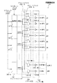
次に、図3〜図5を参照して、垂直駆動回路14の構成について説明する。ここで、図3は垂直駆動回路14の全体構成を表し、図4は図3のVシフトレジスタ141の構成を表し、図5は垂直駆動回路14における各種信号波形を表す。図3に示したように、垂直駆動回路14は、Vシフトレジスタ141と、デコーダ部142と、バッファ部143とを含んで構成されている。
【0019】
Vシフトレジスタ141は複数のパルス転送段141−1〜141−mから構成される。ここで、後述するように、m=M/2である。先頭のパルス転送段141−1には、図1のタイミング発生部30から、図5(b)に示したようなVスタートパルス2VSTが供給され、また、各パルス転送段141−1〜141−mには、タイミング発生部30から、図5(c)に示したようなVクロックパルス2VCKが並列に入力されるようになっている。各パルス転送段141−1〜141−mは、後述するように、1個のインバータとVクロックパルスVCKに同期して動作する2個のクロックトインバータとを用いて構成され、相互に直列接続されている。図示のように、1つのパルス転送段は、画素部11(図2)における2つの画素ラインに対応して設けられている。より具体的には、パルス転送段141−1は画素ラインa1 ,a2 に対応し、パルス転送段141−2は画素ラインa3 ,a4 に対応し、パルス転送段141−mは画素ラインa(M-1) ,aM に対応している。ここで、画素ラインaj (j=1〜M)は、画素部11における画素BD(1,j)〜GD(N,j)からなる画素配列を示す。このような構成のVシフトレジスタ141は、タイミング発生部30から供給されるVスタートパルス2VSTをトリガとして各転送段間のパルス転送動作を開始し、Vクロックパルス2VCKによって定まる時間間隔で、各パルス転送段141−1〜141−mから、それぞれ、図5(d)〜(f)に示したようなシフトレジスタパルスSRP1〜SRPm(但し、図5ではSRP1〜SRP3のみを図示)を順次出力するようになっている。ここで、Vシフトレジスタ141が本発明における「パルス移動手段」に対応し、シフトレジスタパルスSRP1〜SRPmが本発明における「第1のパルス信号」に対応する。
【0020】
図4に示したように、Vシフトレジスタ141のパルス転送段141−1は、クロックトインバータ1411と、クロックトインバータ1411の出力端側に設けられたインバータ1412およびクロックトインバータ1413からなるラッチ回路とを含んでいる。
【0021】
クロックトインバータ1411は、2つのPMOS型のトランジスタ1411a,1411bと、2つのNMOS型のトランジスタ1411c,1411dとを含んで構成されている。トランジスタ1411a,1411bのソース・ドレイン間は相互に接続され、また、トランジスタ1411c,1411dのソース・ドレイン間も相互に接続されている。トランジスタ1411b,1411cはCMOS構造をなし、両者のゲートにはVスタートパルス2VSTが入力されるようになっている。両者のドレインは相互に接続され、出力端として、次段のパルス転送段の入力端(パルス転送段141−2のトランジスタ1411b,1411cのゲート)に接続されている。トランジスタ1411aのソースは電源ラインVDDに接続され、トランジスタ1411dのソースは接地接続されている。トランジスタ1411aのゲートにはVクロックパルス2VCKの反転信号である/2VCKが入力され、トランジスタ1411dのゲートにはVクロックパルス2VCKが入力されるようになっている。
【0022】
インバータ1412は、CMOS構成のトランジスタ1412a,1412bによって構成されており、その入力端(トランジスタ1412a,1412bのゲート)は、クロックトインバータ1411の出力端(トランジスタ1411b,1411cのドレイン)に接続されている。トランジスタ1412aのソースは電源ラインVDDに接続され、トランジスタ1412bのソースは接地接続されている。
【0023】
クロックトインバータ1413は、クロックトインバータ1411と同様の構成であり、2つのPMOS型のトランジスタ1413a,1413bと、2つのNMOS型のトランジスタ1413c,1413dとを含んで構成されている。このクロックトインバータ1413の入力端(CMOS構成をなすトランジスタ1413b,1413cのゲート)は、インバータ1412の出力端(トランジスタ1412a,1412bのドレイン)に接続される一方、出力端(トランジスタ1413b,1413cのドレイン)はインバータ1412の入力端(トランジスタ1412a,1412bのゲート)に接続されている。
【0024】
このような構成のパルス転送段141−1において、クロックトインバータ1411の出力端(トランジスタ1411b,1411cのドレイン)からは、シフトレジスタパルスSRP1が出力され、次段のパルス転送段141−2に転送されると共に、デコーダ部142に入力されるようになっている。他のパルス転送段141−2〜141−mについても同様の構成である。
【0025】
再び図3を参照して説明する。この図に示したように、デコーダ部142は、画素部11の各画素ラインaj ごとに設けられたナンドゲート142−j(j=1〜M)を含んでいる。奇数番目のナンドゲート142−1,142−3等の各一方の入力端には、図5(g)に示したようなデコードパルスVCK−Aが入力され、偶数番目のナンドゲート142−2,142−4等の各一方の入力端には、図5(h)に示したようなデコードパルスVCK−Bが入力されている。ここで、デコードパルスVCK−Aは、Vクロックパルス2VCKの2分の1の周期を有し、デコードパルスVCK−BはデコードパルスVCK−Aを反転した波形を有する。
【0026】
デコーダ部142のナンドゲート142−(2k−1),142−2kの各々他の入力端には、Vシフトレジスタ141のパルス転送段141−kからのシフトレジスタパルスSRPkが入力されるようになっている。ここで、k=1〜mである。これらのナンドゲート142−(2k−1),142−2kは、それぞれ、Vシフトレジスタ141からのシフトレジスタパルスSRPkをデコードパルスVCK−AまたはVCK−Bによってデコードして出力するようになっている。ここで、デコーダ部142が本発明における「個別駆動パルス生成手段」に対応する。
【0027】
バッファ部143は、画素部11の各画素ラインaj ごとに設けられたバッファ143−j(j=1〜M)を含んでいる。各バッファ143−jの入力端はデコーダ部142の各ナンドゲート142−jの出力端に接続され、出力端は画素ラインaj の各画素を構成するTFT(図示せず)のゲートに接続されている。各バッファ143−jは、対応するナンドゲート142−jからの出力信号の論理を反転し、図5(i)〜(n)に示したようなゲートパルスGPj を出力する。これらのゲートパルスGPj は、画素部11の対応する画素ラインaj の各画素を構成するTFTトランジスタのゲート(図示せず)に供給され、各画素を駆動するようになっている。各バッファ143−jはまた、デコーダ部142やVシフトレジスタ141が、画素部11の対応する画素ラインaj における配線容量の影響を受けないうように、両者を隔離する機能をも有している。ここで、ゲートパルスGPj が本発明における「第2のパルス信号」に対応する。
【0028】
次に、以上のような構成のカラー液晶表示装置の動作を説明する。
【0029】
図3において、タイミング発生部30(図1)から出力されるVスタートパルス2VSTはVシフトレジスタ141のパルス転送段141−1に入力され、Vクロックパルス2VCKは、Vシフトレジスタ14の各パルス転送段141−1〜141−mに供給される。これらの各パルス転送段141−1〜141−mは、Vクロックパルス2VCKに従って順次パルス転送を行うと共に、図5(d)〜(f)に示したようなシフトレジスタパルスSRP1〜SRPmを順次出力する。
【0030】
Vシフトレジスタ141の各パルス転送段141−1〜141−mから出力されたシフトレジスタパルスSRP1〜SRPmは、デコーダ部142におけるそれぞれ対応するナンドゲートの組に入力される。より具体的には、シフトレジスタパルスSRPk(k=1〜m)は、対応するナンドゲート142−(2k−1),142−2kに入力される。これらのナンドゲート142−(2k−1),142−2kは、それぞれ、図5(g),(h)に示したようなデコードパルスVCK−A,VCK−BによってシフトレジスタパルスSRPkをデコードして出力する。ナンドゲート142−j(j=1〜M)の出力は、それぞれ、バッファ部143のバッファ143−jによってそれぞれ反転されて、図5(i)〜(n)に示したようなゲートパルスGPj として出力される。ゲートパルスGPj は、画素部11(図2)の対応する画素ラインaj における各画素のTFTトランジスタのゲートに供給され、各トランジスタをオン(開)状態にする。
【0031】
一方、タイミング発生部30(図1)から出力されるHスタートパルスHSTおよびHクロックパルスHCKは、Hシフトレジスタ13(図1)に供給される。Hシフトレジスタ13は、これらの信号HST,HCKに従って水平選択パルスを順次シフトしながら出力する。これらの水平選択パルスは、それぞれ、水平スイッチ部12の上記した各水平スイッチグループに順次入力され、各グループ内の水平スイッチを開状態にする。その結果、第1列から第N列までの各画素列が3列ずつ順次選択される。
【0032】
バッファ部143からのゲートパルスGP1 によって画素ラインa1 が選択されている期間において、Hシフトレジスタ13からの水平選択パルスによって1列から第3列までの画素列が選択されると、信号ドライバ20から入力されるビデオ信号BS,RS,GSは、それぞれ、画素ラインa1 の画素BD(1,1)〜GD(3,1)に供給される。次に、第4列から第6列までの画素列が選択されることにより、ビデオ信号BS,RS,GSはそれぞれ画素BD(4,1)〜GD(6,1)に供給される。以下同様に、画素ラインa1 の画素が順次3個ずつ選択され、それぞれに対してビデオ信号BS,RS,GSが同時に供給される。
【0033】
画素ラインa1 のN個の画素に対するビデオ信号の書込みが終了すると、次に、ゲートパルスGP2 によって画素ラインa2 が選択され、ここでも画素ラインa1 の場合と同様にして3個ずつの画素が選択されて同時にビデオ信号BS,RS,GSが供給される。以下同様にして、1画素ライン分のビデオ信号の供給が終了するたびにゲートパルスGPj によって次の画素ラインが選択される。これにより、1フィールド分の処理が終了する。さらに、1フィールド分の処理が終了すると、次のフィールドにおいても同様の処理が行われる。
【0034】
ここで、図6および図7を参照して、本実施の形態に対する比較例について説明する。
【0035】
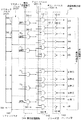
図6は本実施の形態における垂直駆動回路14に対する比較例としての垂直駆動回路114の概略構成を表し、図7は、この垂直駆動回路114における各種信号のタイミングを表すものである。なお、これらの図で本実施の形態(図3,図5)と同一構成部分には同一の符号を付す。図6に示したように、本比較例の垂直駆動回路114は、Vシフトレジスタ1141と、デコーダ部1142と、バッファ部143とを含んで構成されている。Vシフトレジスタ1141は、上記実施の形態におけるVシフトレジスタ141と異なり、画素部11の各画素ラインaj に対応して設けられた合計M(=2m)個のパルス転送段1141−j(j=1〜M)から構成されている。ここで、各パルス転送段1141−jは、上記実施の形態の図4に示した回路と同じ回路構成であり、2つのクロックトインバータと、1つのインバータとによって構成される。Vシフトレジスタ1141には、図7(a)に示したようなVスタートパルスVSTと、図7(b)に示したようなVクロックパルスVCKとが入力される。ここで、VスタートパルスVSTおよびVクロックパルスVCKは、それぞれ、上記実施の形態におけるVスタートパルス2VSTおよびVクロックパルス2VCKのそれぞれ2倍の周波数(2分の1の周期)をもつパルス信号である。
【0036】
Vシフトレジスタ1141の各パルス転送段1141−jは、VスタートパルスVSTおよびVクロックパルスVCKに従ってパルス転送を行い、図7(c)〜(h)に示したようなシフトレジスタパルスSRPj″(この図ではSPR1″〜SPR6″のみを図示)を順次出力して、デコーダ部1142における対応するナンドゲート1142−jに供給するようになっている。デコーダ部1142の各ナンドゲート1142−jは、対応するパルス転送段1141−jから供給されたシフトレジスタパルスSRPj″を、前段のパルス転送段1141−(j−1)からのシフトレジスタパルスSRP(j−1)″によってデコードして出力する。バッファ部143の各バッファ143−jは、対応するナンドゲート1142−jの出力を反転して、図7(i)〜(n)に示したようなゲートパルスGPj を出力し、対応する画素ラインaj に供給するようになっている。
【0037】
このように、本比較例の垂直駆動回路114においては、Vシフトレジスタ1141のパルス転送段1141−jが画素部11の各画素ラインaj ごとに一つずつ設けられている。ここで、1つのパルス転送段1141−jを構成するには、図4に示したように、合計10個のトランジスタ素子が必要であり、各トランジスタ素子間の複雑な配線が必要であることをも考慮すると、かなりの配置面積が必要となる。このため、画素部11の高精細化のために画素ピッチを狭くしようとした場合には、1画素ラインaj の幅に対応する領域に1つのパルス転送段1141−jを形成することが困難となる。例えば、Vシフトレジスタ1141の1つの転送段を図4のように構成する場合には、1画素ライン分の幅領域に10個のトランジスタ素子を配置しなければならず、画素ピッチの狭小化に対応することができない。また、仮に、製造技術の向上に伴うトランジスタ素子のサイズや配線幅の縮小化によって、1画素ラインaj 分の幅領域に1つのパルス転送段1141−jを形成できたとしても、それを製造コストのアップを伴わずに実現することは困難であり、また、画素部11の画素ラインaj の数(=j)を増加した場合には、それに比例してVシフトレジスタ1141の構成に必要な素子数が増加するため、垂直駆動回路114の消費電流が著しく増大することは必至である。さらに、Vシフトレジスタ1141を動作させるためのVスタートパルスVSTやVクロックパルスVCKは、図7(a),(b)に示したように、周波数の高いパルス信号であることから、Vシフトレジスタ1141の各パルス転送段を構成するトランジスタ素子は周波数特性がよいものでなければならず、この点でも構成上の難点がある。
【0038】
これに対して、本実施の形態の垂直駆動回路14によれば、2つの画素ラインに対して1つのパルス転送段を対応付けると共に、各パルス転送段からの出力をデコーダ部142によりデコードして各画素ラインaj 用のゲートパルスGPj を作成するようにしたので、画素ラインの総数が同じであれば、Vシフトレジスタ141の構成段数を上記比較例の2分の1とすることができる。したがって、Vシフトレジスタ141の構成に必要な全素子数を約2分の1にすることが可能であり、消費電流を低減することができる。また、2画素ライン分の幅領域に1つのパルス転送段を形成すればよいことから、画素ピッチを相当狭くしたとしても、現状の製造技術レベルでも十分対応可能である。例えば、Vシフトレジスタ141の1つの転送段を図4のように構成する場合には、2画素ライン分の幅領域に10個のトランジスタ素子を配置すればよく、1画素ライン当たりにすれば5個のトランジスタ素子を配置すればよいこととなるので、製造が容易である。さらに、Vシフトレジスタ141を動作させるためのVスタートパルス2VSTやVクロックパルス2VCKは、図5(b),(c)に示したように、比較例で用いたVスタートパルスVSTおよびVクロックパルスVCK(図7(a),(b))と比べて周波数の低いパルス信号であることから、Vシフトレジスタ141の各パルス転送段を構成するトランジスタ素子は、周波数特性がさほどよいものである必要はなく、通常の特性の素子を使用可能である。
【0039】
なお、本実施の形態では、図3に示したように、デコーダ部142で用いるデコードパルスVCK−A,VCK−Bを、各ナンドゲートごとに交互にA,B,A,B…という順序で割り当てて入力するようにしたが、このほか、図8および図9に示したように、上記のデコードパルスVCK−A,VCK−Bの2倍のパルス幅(2分の1の周波数)をもつデコードパルス2VCK−A,2VCK−Bを用意して、これらをデコーダ部142′の各ナンドゲートにA,B,B,A,A,B,…という順序で割り当てて入力するように変形してもよい。なお、図8は本実施の形態の変形例としての垂直駆動回路14′の概略構成を表し、図9は図8の垂直駆動回路14′の各種信号のタイミングを表すものである。これらの図で、上記の図3および図5に示した各構成部分と同一の構成部分には同一の符号を付し、説明を省略する。図8および図9のうち、デコードパルス2VCK−A,2VCK−Bの波形、およびデコーダ部142′の各ナンドゲートに対するデコードパルス2VCK−A,2VCK−Bの割り当て方法以外の部分の構成は図3および図5と同様である。
【0040】
図8に示した変形例では、図9(g),(h)に示したように、デコードパルス2VCK−A,2VCK−Bの周波数を上記の図5(g),(h)に示したデコードパルスVCK−A,VCK−Bの2分の1にすることができるので、ナンドゲートを構成するトランジスタ素子は高い周波数特性をもつものでなくてもよい。また、図5の例では、例えばタイミングt1,t2において、シフトレジスタパルスSRP1とデコードパルスVCK−AまたはVCK−Bとが同じタイミングで立ち上がり、または立ち下がっているので、両者間にわずかなタイミングずれがあると、ナンドゲートの出力にヒゲ状のスパイクノイズが発生する可能性がある。これに対して、図8に示した変形例では、図9(g),(h)に示したように、シフトレジスタパルスSRP1とデコードパルス2VCK−Aまたは2VCK−Bとの間で、立ち上がりおよび立ち下がりのタイミングは完全に異なっているので、上記のようなヒゲ状のスパイクノイズが発生するおそれは少ない。
【0041】
[第2の実施の形態]
次に、本発明の第2の実施の形態を説明する。
【0042】
図10は本発明の第2の実施の形態に係るカラー液晶表示装置に適用される垂直駆動回路24の概略構成を表すものである。この垂直駆動回路24は、上記第1の実施の形態(図3)におけるVシフトレジスタ141およびデコーダ部142に代えて、それぞれ、Vシフトレジスタ241およびデコーダ部242を備えるようにしたものである。このVシフトレジスタ241は、m1 個のパルス転送段241−1〜241−m1 を含んで構成されている。各パルス転送段241−p(ここで、p=1〜m1 )は、画素部11(図2)の3つの画素ラインa(3p-2), a(3p-1),a(3p)に対して1つずつ設けられており、その内部構成は図4に示したものと同様である。ここで、m1 =M/3(=自然数)である。
【0043】
Vシフトレジスタ241には、図11(b),(c)に示したように、上記比較例(図7(a),(b))におけるVスタートパルスVSTおよびVクロックパルスVCKのそれぞれ3倍の周期をもつVスタートパルス3VSTおよびVクロックパルス3VCKがタイミング発生部30(図1)から供給されるようになっている。ここで、Vシフトレジスタ241が本発明における「パルス移動手段」に対応する。
【0044】
デコーダ部242には、図11(g)〜(i)に示したような互いに異なる位相をもつ3つのデコードパルスVCK−A′,VCK−B′,VCK−C′が供給され、それぞれ、パルス転送段241−pに対応するナンドゲート242−(3p−2),242−(3p−1),242−3pの各々一方の入力端に入力されるようになっている。これらの3個のナンドゲート242−(3p−2),242−(3p−1),242−3pの各々他の入力端には、Vシフトレジスタ241のパルス転送段241−pからシフトレジスタパルスSRPpが入力されるようになっている。デコーダ部242が本発明における「駆動パルス生成手段」に対応し、シフトレジスタパルスSRPpが本発明における「第1のパルス信号」に対応する。
【0045】
次に、このような構成の垂直駆動回路24の動作を説明する。図1のタイミング配線部30から出力されたVスタートパルス3VSTはVシフトレジスタ241のパルス転送段241−1に入力され、Vクロックパルス3VCKは、Vシフトレジスタ24の各パルス転送段241−1〜241−m1 に供給される。これらの各パルス転送段241−1〜241−m1 は、Vクロックパルス3VCKに従って順次パルス転送を行うと共に、図11(d)〜(f)に示したようなシフトレジスタパルスSRP1′〜SRPm1 ′を順次出力する。これらのシフトレジスタパルスSRP1〜SRPm1 ′は、デコーダ部242におけるそれぞれ対応する3個のナンドゲートの組に入力される。より具体的には、シフトレジスタパルスSRPpは3つのナンドゲート242−(3p−2),242−(3p−1),242−3pに入力される。但し、p=1〜m1 である。ナンドゲート242−(3p−2),242−(3p−1),242−3pは、デコードパルスVCK−A,VCK−B,VCK−CによってシフトレジスタパルスSRPpをそれぞれデコードして出力する。これらの各ナンドゲートの出力は、それぞれ、バッファ部143のバッファ143−jによってそれぞれ反転されて、図11(j)〜(o)に示したようなゲートパルスGPj として出力される。ゲートパルスGPj は、画素部11(図2)の対応する画素ラインaj における各画素のTFTトランジスタのゲートに供給され、各トランジスタをオン(開)状態にする。
【0046】
このように、本実施の形態によれば、画素部11の3つの画素ラインに対して1つのパルス転送段241−pを設けるようにしたので、Vシフトレジスタ241の構成に必要な全素子数を上記第1の実施の形態の場合よりもさらに低減することができ、消費電流をより一層低減することができる。また、3画素ライン分の幅領域に1つのパルス転送段を形成すればよいことから、画素ピッチをさらに狭くしたとしても、現状の製造技術レベルで十分対応可能である。例えば、Vシフトレジスタ241の1つの転送段を図4のように構成する場合には、3画素ライン分の幅領域に10個のトランジスタ素子を配置すればよく、1画素ライン当たりにすれば約3個のトランジスタ素子を配置すればよいことから、製造がさらに容易になる。さらに、Vシフトレジスタ241を動作させるためのVスタートパルス3VSTやVクロックパルス3VCKは、図11(b),(c)に示したように、第1の実施の形態で用いるVスタートパルス2VSTおよびVクロックパルス2VCKと比べてより周波数の低いパルス信号であることから、Vシフトレジスタ241の各パルス転送段を構成するトランジスタ素子に要求される周波数特性は、より緩やかなものとなる。
【0047】
[第3の実施の形態]
次に、本発明の第3の実施の形態を説明する。
【0048】
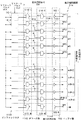
図12は本発明の第3の実施の形態に係るカラー液晶表示装置に適用される垂直駆動回路34の概略構成を表すものである。この垂直駆動回路34は、上記第1の実施の形態(図3)で示した垂直駆動回路14におけるVシフトレジスタ141とデコーダ部142との間に、入力されるビデオ信号の種類(規格)に応じて画素部11(図2)の表示領域をαまたはβに切り替えることを可能とする表示切替回路344を設けたものである。ここで、表示領域αは、画素部11のすべての画素ラインa1 〜aM を表示可能にしたときの表示領域であり、表示領域βは、画素部11の画素ラインのうちa2 〜a(M-1) のみを表示可能にしたときの表示領域である。
【0049】
図12に示したように、表示切替回路344はm個(但し、m=M/2)のナンドゲート344−1〜344−mを含んでいる。各ナンドゲート344−k(但し、k=1〜m)は、Vシフトレジスタ141の各パルス転送段141−kから出力されたシフトレジスタパルスSRPkを後段のデコーダ部142における対応するナンドゲート142−(2k−1),142−2kに入力するか否かを制御するためのものである。ナンドゲート344−kの各々一方の入力端には、シフトレジスタパルスSRPkが入力されるようになっている。また、最上段のナンドゲート344−1および最下段のナンドゲート344−mにおける各々他の入力端には、“H”または“L”レベルのいずれかの値をとる表示切替信号SWが入力されている。その他のナンドゲート344−2〜344−(m−1)における各々他の入力端はすべて“H”レベルに固定されている。その他の構成は図3の場合と同様である。ここで、表示切替回路344が本発明における「切替手段」に対応する。
【0050】
次に、以上のような構成の垂直駆動回路34の動作を説明する。
【0051】
まず、表示領域αを表示可能にする場合には、表示切替回路344のナンドゲート344−1および344−mに入力する表示切替信号SWを“H”レベルにする。これにより、すべてのナンドゲート344−1〜344−mがゲート開状態となり、Vシフトレジスタ141からのすべてのシフトレジスタパルスSRP1〜SRPmがそのままデコーダ部142に供給される。すなわち、この状態では、図3に示した回路状態と等しくなる。画素部11の全体である表示領域αがアクティブ状態となり、ここに画像が表示されることとなる。
【0052】
一方、表示領域βを表示可能にする場合には、表示切替回路344のナンドゲート344−1および344−mに入力する表示切替信号SWを“L”レベルにする。これにより、ナンドゲート344−2〜344−(m−1)のみがゲート開状態となり、ナンドゲート344−1および344−mはゲート閉状態となる。このため、Vシフトレジスタ141からのシフトレジスタパルスSRP1およびSRPmはデコーダ部142に供給されず、シフトレジスタパルスSRP2〜SRP(m−1)のみがそのままデコーダ部142に供給される。これにより、画素部11のうちの表示領域βのみがアクティブ状態となり、ここに画像が表示される。このとき、画素ラインa1 ,a2 ,a(M-1) ,aM の部分は黒く表示される。
【0053】
ここで、本実施の形態の垂直駆動回路34に対する比較例を説明する。
【0054】
図13は本実施の形態に対する比較例としての垂直駆動回路214の概略構成を表すものである。この垂直駆動回路214は、上記第1の実施の形態に対する比較例(図6)で示した垂直駆動回路114におけるデコーダ部1142とバッファ部143との間に、入力されるビデオ信号の種類(規格)に応じて画素部11(図2)の表示領域をαまたはβに切り替えることを可能とする表示切替回路1144を設けたものである。ここで、表示領域α,βは、本実施の形態(図12)におけるものと同じである。表示切替回路1144は、M個のナンドゲート1144−1〜1144−Mから構成されている。これらの各ナンドゲート1144−j(j=1〜M)は画素部11の各画素ラインaj に対応して設けられている。
【0055】
各ナンドゲート1144−jは、デコーダ部1142の各ナンドゲート1142−jの出力を後段のバッファ部143における対応するバッファ143−jに入力するか否かを制御するためのものである。ナンドゲート1144−jの各々一方の入力端には、デコーダ部1142の各ナンドゲート1142−jの出力が入力されるようになっている。また、最上段側の2つのナンドゲート1144−1,1144−2および最下段側の2つのナンドゲート1144−(M−1),1144−Mにおける各々他の入力端には、“H”または“L”レベルのいずれかの値をとる表示切替信号SWが入力されるようになっている。その他のナンドゲート1144−3〜1144−(M−2)における各々他の入力端はすべて“H”レベルに固定されている。その他の構成は図6の場合と同様である。
【0056】
このような構成の垂直駆動回路214において、表示領域αを表示可能にするには、表示切替信号SWを“H”レベルにすることにより、すべてのナンドゲート1144−1〜1144−Mをゲート開状態にする。これにより、デコーダ部1142のすべてのナンドゲート1142−jの出力がそのままバッファ部143の対応するバッファ143−jに供給され、表示領域αがアクティブ状態となる。一方、表示領域βを表示可能にするには、表示切替信号SWを“L”レベルにすることにより、最上段側の2つのナンドゲート1144−1,1144−2および最下段側の2つのナンドゲート1144−(M−1),1144−Mのみをゲート閉状態にする。これにより、これらの4つのナンドゲートの出力はバッファ部143に供給されず、ナンドゲート1144−3〜1144−(M−2)の出力のみがそのままデコーダ部142に供給される。これにより、表示領域βのみがアクティブ状態となり、画素ラインa1 ,a2,a(M-1) ,aM の部分は黒く表示される。
【0057】
このように、本比較例では、画素部11における各画素ラインaj ごとに表示切替用のナンドゲート1144−1〜1144−Mを設けて表示切替回路1144を構成しているので、画素ピッチの狭小化に対応することが上記第1の実施の形態の場合(図3)よりもさらに困難になる。また、表示切替回路1144の構成に必要なトランジスタ素子数が多いので、消費電流が大きくなる。
【0058】
これに対して、本実施の形態の垂直駆動回路34(図12)では、2つの画素ラインa(2k-1),a(2k)の組に対して設けたパルス転送段141−kに対応してナンドゲート1144−kを設けることで表示切替回路344を構成しているので、画素ピッチの狭小化に対応することが上記比較例(図13)の場合よりもさらに容易となる。また、表示切替回路344の構成に必要なトランジスタ素子数を削減できるので、上記比較例(図13)の場合よりも消費電流をさらに低減することができる。
【0059】
なお、本実施の形態では、上記第1の実施の形態に示した垂直駆動回路14に表示切替回路344を設けて表示領域の切り替えを行う場合について説明したが、上記第2の実施の形態に示した垂直駆動回路24(図10)に表示切替回路を設けて表示領域の切り替えを行うことも可能である。この場合には、図10の垂直駆動回路24において、Vシフトレジスタ241のパルス転送段141−p(p=1〜m1 )とデコーダ部242の対応する3個のナンドゲート242−(3p−2),242−(3p−1),242−3pの組との間に1つのナンドゲートを設けるようにして表示切替回路を構成すればよい。
【0060】
以上、いくつかの実施の形態を挙げて本発明を説明したが、本発明はこれらの実施の形態に限定されるものではなく、種々変形可能である。例えば、上記第2の実施の形態では、画素部11における3つの画素ラインa(3p-2),a(3p-1),a(3p)に対して1つのパルス転送段241−pを設けるようにしてVシフトレジスタ241を構成するようにしたが、4つ以上の画素ラインに対して1つのパルス転送段を設けるようにしてもよい。
【0061】
また、上記各実施の形態では、水平方向の駆動方式を3ドット同時サンプリングとしたが、これに限らず、より多くの画素を同時駆動する多ドット同時サンプリングとしてもよく、あるいは1画素ずつ駆動するようにしてもよい。
【0062】
また、本実施の形態ではカラー液晶表示装置について説明したが、本発明はこれに限定されるものではなく、白黒の液晶表示装置にも適用できる。さらに、液晶表示装置以外の表示装置、例えばPD(プラズマディスプレイ)素子やEL(エレクトロ・ルミネセンス)素子、さらには、FED(Field Emission Display)素子等にも適用可能である。なお、このFEDとは、多数の微細な電子源を陰極としてアレイ上に配列すると共に、各陰極に高電圧を印加することにより各陰極から電子を引き出し、これらの電子を陽極に塗布した蛍光体に衝突させて発光させるようにしたものである。
【0063】
【発明の効果】
以上説明したように、請求項1もしくは請求項2記載の画素駆動回路、または請求項3もしくは請求項4記載の駆動回路一体型画素集積装置によれば、画素配列の2つの方向のうちの1の方向に沿って第1のパルス信号を複数画素分ずつ移動させながら順次出力するパルス移動手段を設けると共に、個別駆動パルス生成手段によって、第1のパルス信号を基に、2つの方向のうちの他の方向に沿って配列された画素列を個別に駆動するためのより多くの第2のパルス信号を生成するようにしたので、パルス移動手段を構成する回路素子の数を削減することができる。このため、パルス移動手段を構成する回路の配置面積を縮小できると共に、消費電力の低減が可能になる。また、パルス移動手段は、複数の画素列に対応して1つの第1のパルス信号を出力すればよいので、このパルス移動手段を構成する回路素子に対する周波数特性の要求を緩和することができる。
また、パルス移動手段と個別駆動パルス生成手段との間に、パルス移動手段から個別駆動パルス生成手段に対して第1のパルス信号を供給するか否かを切替可能な切替手段を備えるように構成したので、従来のように個別駆動パルス生成手段と各画素列との間に切替手段を設けるように構成した場合と比べると、切替回路の構成素子数を削減することができ、回路サイズがよりコンパクトとなる。したがって、切替回路によって全画素のうちの一部を選択的に非駆動状態にして表示領域サイズを切り替え可能にする場合においても、従来に比べて消費電力を低減でき、また、画素ピッチの狭小化に対応することができるという効果がある。
【0064】
特に、請求項3または請求項4記載の駆動回路一体型画素集積装置によれば、パルス移動手段を構成する回路素子の数を削減して回路面積を縮小できることから、画素部とその駆動回路とを一体に構成する場合であっても、画素ピッチの狭小化に十分対応することができるという効果がある。
【0065】
また、請求項2記載の画素駆動回路または請求項4記載の駆動回路一体型画素集積装置によれば、切替手段が表示切替信号に応じて、他の方向に沿って配列された画素列のうちの一部の画素列が選択的に非駆動状態となるように第1のパルス信号を供給するか否かの切替を行うように構成したので、表示領域サイズを切り替えることが可能となる。
【図面の簡単な説明】
【図1】本発明の第1の実施の形態に係るカラー液晶表示装置の概略構成を表すブロック図である。
【図2】図1における液晶パネルの概略構成を表す図である。
【図3】図1における垂直駆動回路の概略構成を表す回路図である。
【図4】図3におけるシフトレジスタの各転送段の構成を表す回路図である。
【図5】図3の垂直駆動回路の動作を説明するためのタイミング図である。
【図6】本発明の第1の実施の形態に対する比較例としての垂直駆動回路の概略構成を表す回路図である。
【図7】図6の垂直駆動回路の動作を説明するためのタイミング図である。
【図8】図3の垂直駆動回路に対する変形例を表す回路図である。
【図9】図8の垂直駆動回路の動作を説明するためのタイミング図である。
【図10】本発明の第2の実施の形態に係るカラー液晶表示装置に用いられる垂直駆動回路の概略構成を表すブロック図である。
【図11】図10の垂直駆動回路の動作を説明するためのタイミング図である。
【図12】本発明の第3の実施の形態に係るカラー液晶表示装置に用いられる垂直駆動回路の概略構成を表すブロック図である。
【図13】本発明の第3の実施の形態に対する比較例としての垂直駆動回路の概略構成を表す回路図である。
【符号の説明】
10…液晶パネル、11…画素部、12…水平スイッチ部、13…Hシフトレジスタ、14,14′,24,34…垂直駆動回路、141,241…Vシフトレジスタ、141−1〜141−m,241−1〜241−m1 …パルス転送段、142、142′,242…デコーダ部、143…バッファ部、344…表示切替回路、a1 〜aM …画素ライン、BS,RS,GS…ビデオ信号、2VST,3VST…Vスタートパルス、2VCK,3VCK…Vクロックパルス、VCK−A,VCK−B,2VCK−A,2VCK−B,VCK−A′,VCK−B′,VCK−C′…デコードパルス、SRP1〜SRPm,SRP1〜SRPm1 …シフトレジスタパルス、GP1 〜GPM …ゲートパルス。[0001]
BACKGROUND OF THE INVENTION
The present invention relates to a pixel driving circuit for selectively driving, for example, pixels arranged in a matrix, and a driving circuit integrated pixel integrated device configured to include such a pixel driving circuit.
[0002]
[Prior art]
In recent years, a liquid crystal display device has been widely used as an image display device aligned with a CRT (cathode ray tube). In this device, pixels are arranged in a matrix in the horizontal direction and the vertical direction, and shift registers are arranged in each of the horizontal and vertical directions, and a vertical direction selection pulse is sent from the vertical direction shift register in the vertical direction. Each time a pixel line (a pixel array arranged in a horizontal direction) is selected while being transferred sequentially, a horizontal direction selection pulse is output from the horizontal shift register while being sequentially transferred in a horizontal direction to output a vertical direction selection pulse. By repeating the operation of sequentially selecting the pixels of the pixel line selected by the above while scanning in the horizontal direction, signals are written to all the pixels.
[0003]
By the way, in this type of image display device, the size of the display area is changed in accordance with the type of the image signal so as to be compatible with image signals of various standards as in the case of the image display device using the CRT. There are known multi-scan compatible display devices. In the method used in this type of apparatus, the non-display area (for example, the upper and lower portions of the screen) that is not displayed in the entire screen is blacked without supplying the vertical selection pulse, thereby displaying the display area size. There is a way to adjust. According to this method, since it is not necessary to modify the image signal itself, there is an advantage that a control circuit for image signal processing, an image memory, and the like are unnecessary, and the cost is not significantly increased.
[0004]
[Problems to be solved by the invention]
In the conventional image display device described above, each transfer stage in the vertical shift register is provided corresponding to each pixel line in the vertical direction, and this is output while transferring pulses one by one in the vertical direction. It was a composition. However, recently, when a further reduction in pixel pitch is required in accordance with a demand for higher definition of a display image, a circuit of one transfer stage of a shift register within a width corresponding to one pixel line as in the past. Even if it is going to arrange | position, area becomes inadequate and realization is difficult. Even if such high-density arrangement becomes possible due to improvements in semiconductor device miniaturization technology, if a shift register transfer stage is arranged for each pixel line, the entire shift register Since the number of necessary semiconductor elements such as transistors cannot be reduced, current consumption cannot be reduced. Further, when the pulse transfer of the shift register is performed for each pixel line as in the prior art, it is necessary to increase the transfer speed between the transfer stages of the shift register in order to increase the number of pixel lines. For this reason, it is necessary to increase the operating speed of the semiconductor elements constituting the circuits of the respective transfer stages and other parts (to increase the driving frequency).
[0005]
Further, in the conventional multi-scan display device described above, an opening / closing switch element is provided for each pixel line in order to stop the supply of the selection pulse to the pixel lines in the non-display area of the entire screen. As a result, the number of elements in each stage increases and the current consumption of the entire drive circuit increases. In particular, in a situation where a further reduction in pixel pitch is required, it is difficult to even arrange a circuit of one transfer stage of the shift register within the width of one pixel line as described above. Furthermore, it is almost impossible to arrange a switch element for each pixel line.
[0006]
As described above, in the conventional image display device, it is difficult to reduce the pixel pitch and increase the number of pixels more than the current state, and it is necessary to increase the speed of the elements constituting the drive circuit. there were.
[0007]
The present invention has been made in view of such problems, and its object is to reduce the pixel pitch and reduce the number of pixels without requiring an increase in the number of driving components and a further increase in operation speed. It is an object of the present invention to provide a pixel driving circuit and a driving circuit integrated pixel integrated device that can be easily increased.
[0008]
[Means for Solving the Problems]
The pixel driving circuit of the present invention is a circuit for driving a plurality of pixels arranged in two different directions, and the first pulse signal is divided into a plurality of pixels along one of the two directions. The pixel rows arranged along the other direction of the two directions are individually driven on the basis of the pulse moving means that sequentially outputs while moving each and the first pulse signal output from the pulse moving means. To generate more second pulse signals forIndividualDrive pulse generating means andA switching means provided between the pulse moving means and the individual drive pulse generating means and capable of switching whether or not to supply the first pulse signal from the pulse moving means to the individual drive pulse generating means;It has. here,Whether the switching means supplies the first pulse signal in accordance with the display switching signal so that some of the pixel columns arranged along the other direction are selectively in a non-driven state. It is possible to configure to switch whether or not.
[0009]
The drive circuit integrated pixel integrated device according to the present invention moves a first pulse signal by a plurality of pixels along one direction out of a plurality of pixels arranged in two different directions. Based on the pulse moving means that sequentially outputs and the first pulse signal output from the pulse moving means, more for individually driving pixel columns arranged along the other direction of the two directions. Individual drive pulse generating means for generating the second pulse signal ofA switching means provided between the pulse moving means and the individual drive pulse generating means and capable of switching whether or not to supply the first pulse signal from the pulse moving means to the individual drive pulse generating means;It has. here,Whether the switching means supplies the first pulse signal in accordance with the display switching signal so that some of the pixel columns arranged along the other direction are selectively in a non-driven state. It is possible to configure to switch whether or not.
[0010]
In the pixel driving circuit or the driving circuit integrated pixel integrated device of the present invention, the first pulse signal is sequentially output while moving by a plurality of pixels along one direction by the pulse moving means, and the individual driving pulse generating means Based on the first pulse signal, a second pulse signal for individually driving pixel columns arranged along the other of the two directions is generated.Also,pulseMoveBetween the means and the individual drive pulse generation meansBecause switching means is provided,The first pulse from the pulse moving means to the individual drive pulse generating meanssignalThis makes it possible to switch the effective pixel column range of the pixel columns arranged along the other direction, that is, the displayable region. .In this case, in the switching unit, for example, the first pulse is set so that a part of the pixel columns arranged along the other direction according to the display switching signal is selectively in the non-driven state. Whether to supply a signal is switched.
[0011]
DETAILED DESCRIPTION OF THE INVENTION
Hereinafter, embodiments of the present invention will be described in detail with reference to the drawings. In the following description, the case where the present invention is applied to a color liquid crystal display device in which a pixel portion and a pixel driving circuit are integrally formed on the same substrate will be described.
[0012]
[First Embodiment]
FIG. 1 shows a schematic configuration of a color liquid crystal display device (hereinafter simply referred to as a liquid crystal display device) according to an embodiment of the present invention, which is driven by a so-called active matrix system. As shown in FIG. 1, this apparatus includes a
[0013]
Here, HST represents a start pulse (hereinafter referred to as “H start pulse”) of a horizontal shift register (to be described later) of the
[0014]
FIG. 2 shows a configuration example of the
[0015]
The
[0016]
The
[0017]
The
[0018]
Next, the configuration of the
[0019]
The
[0020]
As shown in FIG. 4, the pulse transfer stage 141-1 of the
[0021]
The clocked
[0022]
The
[0023]
The clocked
[0024]
In the pulse transfer stage 141-1 having such a configuration, the shift register pulse SRP1 is output from the output terminal of the clocked inverter 1411 (the drains of the
[0025]
A description will be given with reference to FIG. 3 again. As shown in this figure, the
[0026]
The shift register pulse SRPk from the pulse transfer stage 141-k of the
[0027]
The
[0028]
Next, the operation of the color liquid crystal display device configured as described above will be described.
[0029]
3, the V start pulse 2VST output from the timing generator 30 (FIG. 1) is input to the pulse transfer stage 141-1 of the
[0030]
The shift register pulses SRP1 to SRPm output from the pulse transfer stages 141-1 to 141-m of the
[0031]
On the other hand, the H start pulse HST and the H clock pulse HCK output from the timing generator 30 (FIG. 1) are supplied to the H shift register 13 (FIG. 1). The
[0032]
If the pixel column from the first column to the third column is selected by the horizontal selection pulse from the
[0033]
When the writing of the video signal to the N pixels of the pixel line a1 is completed, the pixel line a2 is next selected by the gate pulse GP2, and three pixels are selected here as in the case of the pixel line a1. At the same time, video signals BS, RS, and GS are supplied. Similarly, the next pixel line is selected by the gate pulse GPj every time the supply of the video signal for one pixel line is completed. Thereby, the process for one field is completed. Further, when the processing for one field is completed, the same processing is performed in the next field.
[0034]
Here, a comparative example with respect to the present embodiment will be described with reference to FIGS. 6 and 7.
[0035]
FIG. 6 shows a schematic configuration of a vertical drive circuit 114 as a comparative example with respect to the
[0036]
Each pulse transfer stage 1141-j of the
[0037]
Thus, in the vertical drive circuit 114 of this comparative example, one pulse transfer stage 1141-j of the
[0038]
On the other hand, according to the
[0039]
In the present embodiment, as shown in FIG. 3, the decode pulses VCK-A and VCK-B used in the
[0040]
In the modification shown in FIG. 8, as shown in FIGS. 9 (g) and (h), the frequencies of the decode pulses 2VCK-A and 2VCK-B are shown in FIGS. 5 (g) and (h). Since the decode pulses VCK-A and VCK-B can be halved, the transistor elements constituting the NAND gate do not have to have high frequency characteristics. In the example of FIG. 5, for example, at timings t1 and t2, the shift register pulse SRP1 and the decode pulse VCK-A or VCK-B rise or fall at the same timing. If there is, a spike-like spike noise may occur at the output of the NAND gate. On the other hand, in the modification shown in FIG. 8, as shown in FIGS. 9 (g) and (h), the rise and shift between the shift register pulse SRP1 and the decode pulse 2VCK-A or 2VCK-B. Since the falling timing is completely different, there is little possibility that the above-mentioned beard-like spike noise occurs.
[0041]
[Second Embodiment]
Next, a second embodiment of the present invention will be described.
[0042]
FIG. 10 shows a schematic configuration of the
[0043]
As shown in FIGS. 11B and 11C, the
[0044]
The
[0045]
Next, the operation of the
[0046]
Thus, according to the present embodiment, since one pulse transfer stage 241-p is provided for the three pixel lines of the
[0047]
[Third Embodiment]
Next, a third embodiment of the present invention will be described.
[0048]
Figure12These represent the schematic structure of the vertical drive circuit 34 applied to the color liquid crystal display device based on the 3rd Embodiment of this invention. This vertical drive circuit 34 is adapted to the type (standard) of the video signal input between the
[0049]
As shown in FIG. 12, the
[0050]
Next, the operation of the vertical drive circuit 34 configured as described above will be described.
[0051]
First, when the display area α can be displayed, the display switching signal SW input to the NAND gates 344-1 and 344-m of the
[0052]
On the other hand, when the display area β can be displayed, the display switching signal SW input to the NAND gates 344-1 and 344-m of the
[0053]
Here, a comparative example for the vertical drive circuit 34 of the present embodiment will be described.
[0054]
FIG. 13 shows a schematic configuration of a
[0055]
Each NAND gate 1144-j is for controlling whether or not the output of each NAND gate 1142-j of the
[0056]
In the
[0057]
As described above, in this comparative example, the display switching NAND gates 1144-1 to 1144-M are provided for each pixel line aj in the
[0058]
In contrast, the vertical drive circuit 34 (FIG. 12) of the present embodiment corresponds to the pulse transfer stage 141-k provided for the set of two pixel lines a (2k-1) and a (2k). Since the
[0059]
In this embodiment, the case where the
[0060]
Although the present invention has been described with reference to some embodiments, the present invention is not limited to these embodiments and can be variously modified. For example, in the second embodiment, one pulse transfer stage 241-p is provided for three pixel lines a (3p-2), a (3p-1), and a (3p) in the
[0061]
In each of the above embodiments, the horizontal driving method is three-dot simultaneous sampling. However, the present invention is not limited to this, and multi-dot simultaneous sampling for simultaneously driving more pixels may be used, or driving is performed pixel by pixel. You may do it.
[0062]
Further, although a color liquid crystal display device has been described in this embodiment mode, the present invention is not limited to this and can be applied to a monochrome liquid crystal display device. Furthermore, the present invention can be applied to display devices other than liquid crystal display devices, such as PD (plasma display) elements, EL (electroluminescence) elements, and FED (field emission display) elements. The FED is a phosphor in which a large number of fine electron sources are arranged on an array as cathodes, electrons are drawn out from each cathode by applying a high voltage to each cathode, and these electrons are applied to the anode. It is made to emit light by colliding with.
[0063]
【The invention's effect】
As described above, according to the pixel driving circuit according to
In addition, a switching unit is provided between the pulse moving unit and the individual drive pulse generating unit so as to be able to switch whether or not the first pulse signal is supplied from the pulse moving unit to the individual drive pulse generating unit. Therefore, compared to the case where the switching means is provided between the individual drive pulse generating means and each pixel column as in the prior art, the number of constituent elements of the switching circuit can be reduced, and the circuit size is further increased. It becomes compact. Therefore, even when a part of all the pixels is selectively switched to the non-driven state by the switching circuit so that the display area size can be switched, the power consumption can be reduced compared to the conventional case, and the pixel pitch can be narrowed. There is an effect that it can respond to.
[0064]
Particularly, according to the drive circuit integrated pixel integrated device according to
[0065]
Further, according to the pixel drive circuit according to
[Brief description of the drawings]
FIG. 1 is a block diagram showing a schematic configuration of a color liquid crystal display device according to a first embodiment of the invention.
FIG. 2 is a diagram illustrating a schematic configuration of a liquid crystal panel in FIG.
3 is a circuit diagram illustrating a schematic configuration of a vertical drive circuit in FIG. 1. FIG.
4 is a circuit diagram showing a configuration of each transfer stage of the shift register in FIG. 3. FIG.
FIG. 5 is a timing diagram for explaining the operation of the vertical drive circuit of FIG. 3;
FIG. 6 is a circuit diagram showing a schematic configuration of a vertical drive circuit as a comparative example with respect to the first embodiment of the present invention;
7 is a timing chart for explaining the operation of the vertical drive circuit of FIG. 6;
FIG. 8 is a circuit diagram illustrating a modification of the vertical drive circuit of FIG.
9 is a timing chart for explaining the operation of the vertical drive circuit of FIG.
FIG. 10 is a block diagram showing a schematic configuration of a vertical drive circuit used in a color liquid crystal display device according to a second embodiment of the present invention.
11 is a timing chart for explaining the operation of the vertical drive circuit of FIG.
FIG. 12 is a block diagram showing a schematic configuration of a vertical drive circuit used in a color liquid crystal display device according to a third embodiment of the present invention.
FIG. 13 is a circuit diagram illustrating a schematic configuration of a vertical drive circuit as a comparative example with respect to the third embodiment of the present invention.
[Explanation of symbols]
DESCRIPTION OF
Claims (4)
前記2つの方向のうちの1の方向に沿って第1のパルス信号を複数画素分ずつ移動させながら順次出力するパルス移動手段と、
前記パルス移動手段から出力された第1のパルス信号を基に、前記2つの方向のうちの他の方向に沿って配列された画素列を個別に駆動するためのより多くの第2のパルス信号を生成する個別駆動パルス生成手段と、
前記パルス移動手段と前記個別駆動パルス生成手段との間に設けられ、パルス移動手段から個別駆動パルス生成手段に対して前記第1のパルス信号を供給するか否かを切替可能な切替手段と
を備えたことを特徴とする画素駆動回路。A circuit for driving a plurality of pixels arranged in two different directions,
Pulse moving means for sequentially outputting the first pulse signal while moving the first pulse signal by a plurality of pixels along one of the two directions;
More second pulse signals for individually driving pixel columns arranged along the other direction of the two directions based on the first pulse signal output from the pulse moving means and individual drive pulse generating means for generating a,
Switching means provided between the pulse moving means and the individual drive pulse generating means, and capable of switching whether or not to supply the first pulse signal from the pulse moving means to the individual drive pulse generating means. A pixel driving circuit comprising:
ことを特徴とする請求項1記載の画素駆動回路。 In accordance with a display switching signal, the switching means is configured to select the first pulse signal so that some of the pixel columns arranged along the other direction are selectively in a non-driven state. The pixel driving circuit according to claim 1 , wherein switching is performed to determine whether or not to supply the pixel.
前記2つの方向のうちの1の方向に沿って第1のパルス信号を複数画素分ずつ移動させながら順次出力するパルス移動手段と、
前記パルス移動手段から出力された第1のパルス信号を基に、前記2つの方向のうちの他の方向に沿って配列された画素列を個別に駆動するためのより多くの第2のパルス信号を生成する個別駆動パルス生成手段と、
前記パルス移動手段と前記個別駆動パルス生成手段との間に設けられ、パルス移動手段から個別駆動パルス生成手段に対して前記第1のパルス信号を供給するか否かを切替可能な切替手段と
を備えたことを特徴とする駆動回路一体型画素集積装置。A plurality of pixels arranged in two different directions;
Pulse moving means for sequentially outputting the first pulse signal while moving the first pulse signal by a plurality of pixels along one of the two directions;
More second pulse signals for individually driving pixel columns arranged along the other direction of the two directions based on the first pulse signal output from the pulse moving means and individual drive pulse generating means for generating a,
Switching means provided between the pulse moving means and the individual drive pulse generating means, and capable of switching whether or not to supply the first pulse signal from the pulse moving means to the individual drive pulse generating means. A drive circuit-integrated pixel integrated device.
ことを特徴とする請求項3記載の駆動回路一体型画素集積装置。 In accordance with a display switching signal, the switching means is configured to select the first pulse signal so that some of the pixel columns arranged along the other direction are selectively in a non-driven state. 4. The drive circuit integrated pixel integrated device according to claim 3, wherein whether or not to supply is switched .
Priority Applications (4)
| Application Number | Priority Date | Filing Date | Title |
|---|---|---|---|
| JP09450898A JP3972270B2 (en) | 1998-04-07 | 1998-04-07 | Pixel driving circuit and driving circuit integrated pixel integrated device |
| NL1011715A NL1011715C2 (en) | 1998-04-07 | 1999-04-01 | Pixel driver, combination of a pixel driver / integrated element element, and liquid crystal display device. |
| US09/285,784 US6630920B1 (en) | 1998-04-07 | 1999-04-05 | Pel drive circuit, combination pel-drive-circuit/pel-integrated device, and liquid crystal display device |
| KR1019990011857A KR100611595B1 (en) | 1998-04-07 | 1999-04-06 | Pixel driving circuit, pixel integrating device incorporated with a driving circuit and liquid crystal display device |
Applications Claiming Priority (1)
| Application Number | Priority Date | Filing Date | Title |
|---|---|---|---|
| JP09450898A JP3972270B2 (en) | 1998-04-07 | 1998-04-07 | Pixel driving circuit and driving circuit integrated pixel integrated device |
Publications (2)
| Publication Number | Publication Date |
|---|---|
| JPH11296129A JPH11296129A (en) | 1999-10-29 |
| JP3972270B2 true JP3972270B2 (en) | 2007-09-05 |
Family
ID=14112271
Family Applications (1)
| Application Number | Title | Priority Date | Filing Date |
|---|---|---|---|
| JP09450898A Expired - Fee Related JP3972270B2 (en) | 1998-04-07 | 1998-04-07 | Pixel driving circuit and driving circuit integrated pixel integrated device |
Country Status (4)
| Country | Link |
|---|---|
| US (1) | US6630920B1 (en) |
| JP (1) | JP3972270B2 (en) |
| KR (1) | KR100611595B1 (en) |
| NL (1) | NL1011715C2 (en) |
Families Citing this family (27)
| Publication number | Priority date | Publication date | Assignee | Title |
|---|---|---|---|---|
| US6437766B1 (en) | 1998-03-30 | 2002-08-20 | Sharp Kabushiki Kaisha | LCD driving circuitry with reduced number of control signals |
| JP2000227784A (en) | 1998-07-29 | 2000-08-15 | Seiko Epson Corp | Driving circuit for electro-optical device, and electro- optical device |
| JP4747426B2 (en) * | 2001-03-14 | 2011-08-17 | 日本テキサス・インスツルメンツ株式会社 | Driving circuit |
| US6967639B2 (en) * | 2001-09-26 | 2005-11-22 | International Business Machines Corporation | Image display device, scan line drive circuit and driver circuit for display device |
| JP3968499B2 (en) * | 2001-10-17 | 2007-08-29 | ソニー株式会社 | Display device |
| JP3613240B2 (en) * | 2001-12-05 | 2005-01-26 | セイコーエプソン株式会社 | Display driving circuit, electro-optical device, and display driving method |
| KR100800466B1 (en) * | 2001-12-24 | 2008-02-04 | 삼성전자주식회사 | TFT LCD driver capable of reducing chip size |
| KR100840682B1 (en) * | 2002-09-06 | 2008-06-24 | 엘지디스플레이 주식회사 | Liquid crystal dispaly apparatus of line on glass type |
| JP3797337B2 (en) * | 2003-02-25 | 2006-07-19 | ソニー株式会社 | Shift register and display device |
| TWI244060B (en) * | 2003-06-12 | 2005-11-21 | Ind Tech Res Inst | A scan driving circuit with single-type transistors |
| JP2005234057A (en) | 2004-02-17 | 2005-09-02 | Sharp Corp | Image display device |
| JP3839460B2 (en) * | 2004-02-24 | 2006-11-01 | 丸文株式会社 | Hold-type display device and parts thereof |
| JP4525152B2 (en) * | 2004-04-16 | 2010-08-18 | セイコーエプソン株式会社 | Electro-optical device drive circuit, electro-optical device drive method, and electro-optical device and electronic apparatus including the same |
| KR100624306B1 (en) * | 2004-05-28 | 2006-09-18 | 삼성에스디아이 주식회사 | Scan driving apparatus and having the flat panel display and driving method thereof |
| JP4999352B2 (en) * | 2005-05-02 | 2012-08-15 | 株式会社半導体エネルギー研究所 | Display device and electronic device |
| KR101160836B1 (en) * | 2005-09-27 | 2012-06-29 | 삼성전자주식회사 | Display device and shift register therefor |
| JP2008076443A (en) * | 2006-09-19 | 2008-04-03 | Toshiba Matsushita Display Technology Co Ltd | Liquid crystal display device |
| JP2008145921A (en) * | 2006-12-13 | 2008-06-26 | Toppoly Optoelectronics Corp | Driving circuit for active matrix display device |
| JP5076741B2 (en) * | 2007-08-30 | 2012-11-21 | セイコーエプソン株式会社 | Electro-optical device, drive circuit for electro-optical device, and electronic apparatus |
| KR101904811B1 (en) * | 2009-07-24 | 2018-10-05 | 가부시키가이샤 한도오따이 에네루기 켄큐쇼 | Semiconductor device |
| JPWO2012014361A1 (en) | 2010-07-30 | 2013-09-09 | パナソニック株式会社 | Display panel drive device |
| KR101778650B1 (en) * | 2011-02-23 | 2017-09-15 | 삼성디스플레이 주식회사 | Display panel and display apparatus having the same |
| US8773413B2 (en) * | 2011-09-13 | 2014-07-08 | Shenzhen China Star Optoelectronics Technology Co., Ltd. | Liquid crystal display panel, liquid crystal display device, and gate driving method of liquid crystal display panel |
| CN102290040B (en) * | 2011-09-13 | 2013-09-04 | 深圳市华星光电技术有限公司 | Liquid crystal panel, liquid crystal display device and method for driving gate of liquid crystal panel |
| JP6017214B2 (en) | 2012-07-23 | 2016-10-26 | ソニーセミコンダクタソリューションズ株式会社 | Imaging device, driving method of imaging device, and imaging display system |
| CN103345911B (en) | 2013-06-26 | 2016-02-17 | 京东方科技集团股份有限公司 | A kind of shift register cell, gate driver circuit and display device |
| CN105225625B (en) | 2015-11-05 | 2018-01-23 | 京东方科技集团股份有限公司 | Shift register cell, gate driving circuit and its driving method, display device |
Family Cites Families (11)
| Publication number | Priority date | Publication date | Assignee | Title |
|---|---|---|---|---|
| JPS6039180B2 (en) * | 1978-11-28 | 1985-09-04 | 日本電気株式会社 | sense amplifier |
| JPS56130885A (en) * | 1980-03-18 | 1981-10-14 | Fujitsu Ltd | Address buffer circuit |
| JPS61126595A (en) * | 1984-11-26 | 1986-06-14 | キヤノン株式会社 | Active matrix circuit substrate |
| US5222082A (en) * | 1991-02-28 | 1993-06-22 | Thomson Consumer Electronics, S.A. | Shift register useful as a select line scanner for liquid crystal display |
| US5410583A (en) * | 1993-10-28 | 1995-04-25 | Rca Thomson Licensing Corporation | Shift register useful as a select line scanner for a liquid crystal display |
| US5434899A (en) * | 1994-08-12 | 1995-07-18 | Thomson Consumer Electronics, S.A. | Phase clocked shift register with cross connecting between stages |
| US5517542A (en) * | 1995-03-06 | 1996-05-14 | Thomson Consumer Electronics, S.A. | Shift register with a transistor operating in a low duty cycle |
| US6040812A (en) * | 1996-06-19 | 2000-03-21 | Xerox Corporation | Active matrix display with integrated drive circuitry |
| KR100492952B1 (en) * | 1997-11-05 | 2005-11-01 | 엘지전자 주식회사 | Scanning Electrode Control for Driving High Resolution AC PD |
| KR100556455B1 (en) * | 1998-09-26 | 2006-05-25 | 엘지전자 주식회사 | gate driving circuit of TFT-LCD |
| KR100500414B1 (en) * | 1998-10-28 | 2005-09-02 | 주식회사 하이닉스반도체 | Test Mode Enable Signaling Circuit of Semiconductor Memory Device |
-
1998
- 1998-04-07 JP JP09450898A patent/JP3972270B2/en not_active Expired - Fee Related
-
1999
- 1999-04-01 NL NL1011715A patent/NL1011715C2/en not_active IP Right Cessation
- 1999-04-05 US US09/285,784 patent/US6630920B1/en not_active Expired - Fee Related
- 1999-04-06 KR KR1019990011857A patent/KR100611595B1/en not_active IP Right Cessation
Also Published As
| Publication number | Publication date |
|---|---|
| KR100611595B1 (en) | 2006-08-10 |
| US6630920B1 (en) | 2003-10-07 |
| JPH11296129A (en) | 1999-10-29 |
| NL1011715C2 (en) | 2007-09-10 |
| KR19990082955A (en) | 1999-11-25 |
| NL1011715A1 (en) | 1999-10-08 |
Similar Documents
| Publication | Publication Date | Title |
|---|---|---|
| JP3972270B2 (en) | Pixel driving circuit and driving circuit integrated pixel integrated device | |
| US7508479B2 (en) | Liquid crystal display | |
| US6989810B2 (en) | Liquid crystal display and data latch circuit | |
| US6542139B1 (en) | Matrix type display apparatus | |
| EP0676078B1 (en) | A select driver circuit for an lcd display | |
| US20100134474A1 (en) | Scan signal line driver circuit, display device, and method of driving scan signal lines | |
| US20040041769A1 (en) | Display apparatus | |
| JP2000089194A (en) | Display device and its drive assembly and drive method | |
| JPH1073843A (en) | Active matrix type liquid crystal display device | |
| JP2010033038A (en) | Display panel driving method, and display | |
| JP2004046066A (en) | Signal output device and display device | |
| KR100306720B1 (en) | Active matrix drive circuit | |
| JPH10260661A (en) | Driving circuit for display device | |
| JPH05313129A (en) | Liquid crystal display device | |
| JP3090922B2 (en) | Flat display device, array substrate, and method of driving flat display device | |
| JP2002169518A (en) | Liquid crystal display device | |
| JP2004226684A (en) | Image display panel and image display device | |
| US6362804B1 (en) | Liquid crystal display with picture displaying function for displaying a picture in an aspect ratio different from the normal aspect ratio | |
| JPH09146489A (en) | Scanning circuit and image display device | |
| TWI301262B (en) | ||
| JPH0968690A (en) | Driving device for flat surface display device | |
| JP2001337657A (en) | Liquid crystal display device | |
| JPH0854601A (en) | Active matrix type liquid crystal display device | |
| WO2000045364A1 (en) | Liquid crystal driving method and liquid crystal driving circuit | |
| JP3230408B2 (en) | Display device |
Legal Events
| Date | Code | Title | Description |
|---|---|---|---|
| A521 | Request for written amendment filed |
Free format text: JAPANESE INTERMEDIATE CODE: A523 Effective date: 20050105 |
|
| A621 | Written request for application examination |
Free format text: JAPANESE INTERMEDIATE CODE: A621 Effective date: 20050105 |
|
| A977 | Report on retrieval |
Free format text: JAPANESE INTERMEDIATE CODE: A971007 Effective date: 20060911 |
|
| A131 | Notification of reasons for refusal |
Free format text: JAPANESE INTERMEDIATE CODE: A131 Effective date: 20060919 |
|
| A521 | Request for written amendment filed |
Free format text: JAPANESE INTERMEDIATE CODE: A523 Effective date: 20061120 |
|
| TRDD | Decision of grant or rejection written | ||
| A01 | Written decision to grant a patent or to grant a registration (utility model) |
Free format text: JAPANESE INTERMEDIATE CODE: A01 Effective date: 20070518 |
|
| A61 | First payment of annual fees (during grant procedure) |
Free format text: JAPANESE INTERMEDIATE CODE: A61 Effective date: 20070531 |
|
| FPAY | Renewal fee payment (event date is renewal date of database) |
Free format text: PAYMENT UNTIL: 20100622 Year of fee payment: 3 |
|
| FPAY | Renewal fee payment (event date is renewal date of database) |
Free format text: PAYMENT UNTIL: 20100622 Year of fee payment: 3 |
|
| FPAY | Renewal fee payment (event date is renewal date of database) |
Free format text: PAYMENT UNTIL: 20110622 Year of fee payment: 4 |
|
| FPAY | Renewal fee payment (event date is renewal date of database) |
Free format text: PAYMENT UNTIL: 20120622 Year of fee payment: 5 |
|
| FPAY | Renewal fee payment (event date is renewal date of database) |
Free format text: PAYMENT UNTIL: 20120622 Year of fee payment: 5 |
|
| FPAY | Renewal fee payment (event date is renewal date of database) |
Free format text: PAYMENT UNTIL: 20130622 Year of fee payment: 6 |
|
| R250 | Receipt of annual fees |
Free format text: JAPANESE INTERMEDIATE CODE: R250 |
|
| R250 | Receipt of annual fees |
Free format text: JAPANESE INTERMEDIATE CODE: R250 |
|
| LAPS | Cancellation because of no payment of annual fees |