KR100743331B1 - Phosphor and Optical Device Using Same - Google Patents
Phosphor and Optical Device Using Same Download PDFInfo
- Publication number
- KR100743331B1 KR100743331B1 KR1020057011597A KR20057011597A KR100743331B1 KR 100743331 B1 KR100743331 B1 KR 100743331B1 KR 1020057011597 A KR1020057011597 A KR 1020057011597A KR 20057011597 A KR20057011597 A KR 20057011597A KR 100743331 B1 KR100743331 B1 KR 100743331B1
- Authority
- KR
- South Korea
- Prior art keywords
- light
- light emitting
- delete delete
- led
- led element
- Prior art date
Links
Images


Classifications
-
- C—CHEMISTRY; METALLURGY
- C09—DYES; PAINTS; POLISHES; NATURAL RESINS; ADHESIVES; COMPOSITIONS NOT OTHERWISE PROVIDED FOR; APPLICATIONS OF MATERIALS NOT OTHERWISE PROVIDED FOR
- C09K—MATERIALS FOR MISCELLANEOUS APPLICATIONS, NOT PROVIDED FOR ELSEWHERE
- C09K11/00—Luminescent, e.g. electroluminescent, chemiluminescent materials
- C09K11/08—Luminescent, e.g. electroluminescent, chemiluminescent materials containing inorganic luminescent materials
- C09K11/74—Luminescent, e.g. electroluminescent, chemiluminescent materials containing inorganic luminescent materials containing arsenic, antimony or bismuth
- C09K11/75—Luminescent, e.g. electroluminescent, chemiluminescent materials containing inorganic luminescent materials containing arsenic, antimony or bismuth containing antimony
- C09K11/757—Aluminates; Silicates
-
- C—CHEMISTRY; METALLURGY
- C09—DYES; PAINTS; POLISHES; NATURAL RESINS; ADHESIVES; COMPOSITIONS NOT OTHERWISE PROVIDED FOR; APPLICATIONS OF MATERIALS NOT OTHERWISE PROVIDED FOR
- C09K—MATERIALS FOR MISCELLANEOUS APPLICATIONS, NOT PROVIDED FOR ELSEWHERE
- C09K11/00—Luminescent, e.g. electroluminescent, chemiluminescent materials
- C09K11/08—Luminescent, e.g. electroluminescent, chemiluminescent materials containing inorganic luminescent materials
- C09K11/74—Luminescent, e.g. electroluminescent, chemiluminescent materials containing inorganic luminescent materials containing arsenic, antimony or bismuth
- C09K11/75—Luminescent, e.g. electroluminescent, chemiluminescent materials containing inorganic luminescent materials containing arsenic, antimony or bismuth containing antimony
-
- C—CHEMISTRY; METALLURGY
- C09—DYES; PAINTS; POLISHES; NATURAL RESINS; ADHESIVES; COMPOSITIONS NOT OTHERWISE PROVIDED FOR; APPLICATIONS OF MATERIALS NOT OTHERWISE PROVIDED FOR
- C09K—MATERIALS FOR MISCELLANEOUS APPLICATIONS, NOT PROVIDED FOR ELSEWHERE
- C09K11/00—Luminescent, e.g. electroluminescent, chemiluminescent materials
- C09K11/08—Luminescent, e.g. electroluminescent, chemiluminescent materials containing inorganic luminescent materials
- C09K11/0844—Germanates
-
- C—CHEMISTRY; METALLURGY
- C09—DYES; PAINTS; POLISHES; NATURAL RESINS; ADHESIVES; COMPOSITIONS NOT OTHERWISE PROVIDED FOR; APPLICATIONS OF MATERIALS NOT OTHERWISE PROVIDED FOR
- C09K—MATERIALS FOR MISCELLANEOUS APPLICATIONS, NOT PROVIDED FOR ELSEWHERE
- C09K11/00—Luminescent, e.g. electroluminescent, chemiluminescent materials
- C09K11/08—Luminescent, e.g. electroluminescent, chemiluminescent materials containing inorganic luminescent materials
- C09K11/0894—Antimonates; Arsenates
-
- C—CHEMISTRY; METALLURGY
- C09—DYES; PAINTS; POLISHES; NATURAL RESINS; ADHESIVES; COMPOSITIONS NOT OTHERWISE PROVIDED FOR; APPLICATIONS OF MATERIALS NOT OTHERWISE PROVIDED FOR
- C09K—MATERIALS FOR MISCELLANEOUS APPLICATIONS, NOT PROVIDED FOR ELSEWHERE
- C09K11/00—Luminescent, e.g. electroluminescent, chemiluminescent materials
- C09K11/08—Luminescent, e.g. electroluminescent, chemiluminescent materials containing inorganic luminescent materials
- C09K11/59—Luminescent, e.g. electroluminescent, chemiluminescent materials containing inorganic luminescent materials containing silicon
- C09K11/592—Chalcogenides
- C09K11/595—Chalcogenides with zinc or cadmium
-
- C—CHEMISTRY; METALLURGY
- C09—DYES; PAINTS; POLISHES; NATURAL RESINS; ADHESIVES; COMPOSITIONS NOT OTHERWISE PROVIDED FOR; APPLICATIONS OF MATERIALS NOT OTHERWISE PROVIDED FOR
- C09K—MATERIALS FOR MISCELLANEOUS APPLICATIONS, NOT PROVIDED FOR ELSEWHERE
- C09K11/00—Luminescent, e.g. electroluminescent, chemiluminescent materials
- C09K11/08—Luminescent, e.g. electroluminescent, chemiluminescent materials containing inorganic luminescent materials
- C09K11/64—Luminescent, e.g. electroluminescent, chemiluminescent materials containing inorganic luminescent materials containing aluminium
- C09K11/641—Chalcogenides
- C09K11/643—Chalcogenides with alkaline earth metals
-
- C—CHEMISTRY; METALLURGY
- C09—DYES; PAINTS; POLISHES; NATURAL RESINS; ADHESIVES; COMPOSITIONS NOT OTHERWISE PROVIDED FOR; APPLICATIONS OF MATERIALS NOT OTHERWISE PROVIDED FOR
- C09K—MATERIALS FOR MISCELLANEOUS APPLICATIONS, NOT PROVIDED FOR ELSEWHERE
- C09K11/00—Luminescent, e.g. electroluminescent, chemiluminescent materials
- C09K11/08—Luminescent, e.g. electroluminescent, chemiluminescent materials containing inorganic luminescent materials
- C09K11/66—Luminescent, e.g. electroluminescent, chemiluminescent materials containing inorganic luminescent materials containing germanium, tin or lead
- C09K11/666—Aluminates; Silicates
-
- C—CHEMISTRY; METALLURGY
- C09—DYES; PAINTS; POLISHES; NATURAL RESINS; ADHESIVES; COMPOSITIONS NOT OTHERWISE PROVIDED FOR; APPLICATIONS OF MATERIALS NOT OTHERWISE PROVIDED FOR
- C09K—MATERIALS FOR MISCELLANEOUS APPLICATIONS, NOT PROVIDED FOR ELSEWHERE
- C09K11/00—Luminescent, e.g. electroluminescent, chemiluminescent materials
- C09K11/08—Luminescent, e.g. electroluminescent, chemiluminescent materials containing inorganic luminescent materials
- C09K11/70—Luminescent, e.g. electroluminescent, chemiluminescent materials containing inorganic luminescent materials containing phosphorus
- C09K11/71—Luminescent, e.g. electroluminescent, chemiluminescent materials containing inorganic luminescent materials containing phosphorus also containing alkaline earth metals
-
- C—CHEMISTRY; METALLURGY
- C09—DYES; PAINTS; POLISHES; NATURAL RESINS; ADHESIVES; COMPOSITIONS NOT OTHERWISE PROVIDED FOR; APPLICATIONS OF MATERIALS NOT OTHERWISE PROVIDED FOR
- C09K—MATERIALS FOR MISCELLANEOUS APPLICATIONS, NOT PROVIDED FOR ELSEWHERE
- C09K11/00—Luminescent, e.g. electroluminescent, chemiluminescent materials
- C09K11/08—Luminescent, e.g. electroluminescent, chemiluminescent materials containing inorganic luminescent materials
- C09K11/74—Luminescent, e.g. electroluminescent, chemiluminescent materials containing inorganic luminescent materials containing arsenic, antimony or bismuth
- C09K11/75—Luminescent, e.g. electroluminescent, chemiluminescent materials containing inorganic luminescent materials containing arsenic, antimony or bismuth containing antimony
- C09K11/751—Chalcogenides
- C09K11/753—Chalcogenides with alkaline earth metals
-
- C—CHEMISTRY; METALLURGY
- C09—DYES; PAINTS; POLISHES; NATURAL RESINS; ADHESIVES; COMPOSITIONS NOT OTHERWISE PROVIDED FOR; APPLICATIONS OF MATERIALS NOT OTHERWISE PROVIDED FOR
- C09K—MATERIALS FOR MISCELLANEOUS APPLICATIONS, NOT PROVIDED FOR ELSEWHERE
- C09K11/00—Luminescent, e.g. electroluminescent, chemiluminescent materials
- C09K11/08—Luminescent, e.g. electroluminescent, chemiluminescent materials containing inorganic luminescent materials
- C09K11/74—Luminescent, e.g. electroluminescent, chemiluminescent materials containing inorganic luminescent materials containing arsenic, antimony or bismuth
- C09K11/75—Luminescent, e.g. electroluminescent, chemiluminescent materials containing inorganic luminescent materials containing arsenic, antimony or bismuth containing antimony
- C09K11/755—Halogenides
- C09K11/756—Halogenides with alkali or alkaline earth metals
-
- C—CHEMISTRY; METALLURGY
- C09—DYES; PAINTS; POLISHES; NATURAL RESINS; ADHESIVES; COMPOSITIONS NOT OTHERWISE PROVIDED FOR; APPLICATIONS OF MATERIALS NOT OTHERWISE PROVIDED FOR
- C09K—MATERIALS FOR MISCELLANEOUS APPLICATIONS, NOT PROVIDED FOR ELSEWHERE
- C09K11/00—Luminescent, e.g. electroluminescent, chemiluminescent materials
- C09K11/08—Luminescent, e.g. electroluminescent, chemiluminescent materials containing inorganic luminescent materials
- C09K11/77—Luminescent, e.g. electroluminescent, chemiluminescent materials containing inorganic luminescent materials containing rare earth metals
- C09K11/7728—Luminescent, e.g. electroluminescent, chemiluminescent materials containing inorganic luminescent materials containing rare earth metals containing europium
- C09K11/77342—Silicates
-
- C—CHEMISTRY; METALLURGY
- C09—DYES; PAINTS; POLISHES; NATURAL RESINS; ADHESIVES; COMPOSITIONS NOT OTHERWISE PROVIDED FOR; APPLICATIONS OF MATERIALS NOT OTHERWISE PROVIDED FOR
- C09K—MATERIALS FOR MISCELLANEOUS APPLICATIONS, NOT PROVIDED FOR ELSEWHERE
- C09K11/00—Luminescent, e.g. electroluminescent, chemiluminescent materials
- C09K11/08—Luminescent, e.g. electroluminescent, chemiluminescent materials containing inorganic luminescent materials
- C09K11/77—Luminescent, e.g. electroluminescent, chemiluminescent materials containing inorganic luminescent materials containing rare earth metals
- C09K11/7728—Luminescent, e.g. electroluminescent, chemiluminescent materials containing inorganic luminescent materials containing rare earth metals containing europium
- C09K11/7735—Germanates
-
- C—CHEMISTRY; METALLURGY
- C09—DYES; PAINTS; POLISHES; NATURAL RESINS; ADHESIVES; COMPOSITIONS NOT OTHERWISE PROVIDED FOR; APPLICATIONS OF MATERIALS NOT OTHERWISE PROVIDED FOR
- C09K—MATERIALS FOR MISCELLANEOUS APPLICATIONS, NOT PROVIDED FOR ELSEWHERE
- C09K11/00—Luminescent, e.g. electroluminescent, chemiluminescent materials
- C09K11/08—Luminescent, e.g. electroluminescent, chemiluminescent materials containing inorganic luminescent materials
- C09K11/77—Luminescent, e.g. electroluminescent, chemiluminescent materials containing inorganic luminescent materials containing rare earth metals
- C09K11/7728—Luminescent, e.g. electroluminescent, chemiluminescent materials containing inorganic luminescent materials containing rare earth metals containing europium
- C09K11/7737—Phosphates
- C09K11/7738—Phosphates with alkaline earth metals
- C09K11/7739—Phosphates with alkaline earth metals with halogens
-
- H—ELECTRICITY
- H01—ELECTRIC ELEMENTS
- H01L—SEMICONDUCTOR DEVICES NOT COVERED BY CLASS H10
- H01L2224/00—Indexing scheme for arrangements for connecting or disconnecting semiconductor or solid-state bodies and methods related thereto as covered by H01L24/00
- H01L2224/01—Means for bonding being attached to, or being formed on, the surface to be connected, e.g. chip-to-package, die-attach, "first-level" interconnects; Manufacturing methods related thereto
- H01L2224/10—Bump connectors; Manufacturing methods related thereto
- H01L2224/15—Structure, shape, material or disposition of the bump connectors after the connecting process
- H01L2224/16—Structure, shape, material or disposition of the bump connectors after the connecting process of an individual bump connector
- H01L2224/161—Disposition
- H01L2224/16135—Disposition the bump connector connecting between different semiconductor or solid-state bodies, i.e. chip-to-chip
- H01L2224/16145—Disposition the bump connector connecting between different semiconductor or solid-state bodies, i.e. chip-to-chip the bodies being stacked
-
- H—ELECTRICITY
- H01—ELECTRIC ELEMENTS
- H01L—SEMICONDUCTOR DEVICES NOT COVERED BY CLASS H10
- H01L2224/00—Indexing scheme for arrangements for connecting or disconnecting semiconductor or solid-state bodies and methods related thereto as covered by H01L24/00
- H01L2224/01—Means for bonding being attached to, or being formed on, the surface to be connected, e.g. chip-to-package, die-attach, "first-level" interconnects; Manufacturing methods related thereto
- H01L2224/42—Wire connectors; Manufacturing methods related thereto
- H01L2224/47—Structure, shape, material or disposition of the wire connectors after the connecting process
- H01L2224/48—Structure, shape, material or disposition of the wire connectors after the connecting process of an individual wire connector
- H01L2224/4805—Shape
- H01L2224/4809—Loop shape
- H01L2224/48091—Arched
-
- H—ELECTRICITY
- H01—ELECTRIC ELEMENTS
- H01L—SEMICONDUCTOR DEVICES NOT COVERED BY CLASS H10
- H01L2224/00—Indexing scheme for arrangements for connecting or disconnecting semiconductor or solid-state bodies and methods related thereto as covered by H01L24/00
- H01L2224/01—Means for bonding being attached to, or being formed on, the surface to be connected, e.g. chip-to-package, die-attach, "first-level" interconnects; Manufacturing methods related thereto
- H01L2224/42—Wire connectors; Manufacturing methods related thereto
- H01L2224/47—Structure, shape, material or disposition of the wire connectors after the connecting process
- H01L2224/48—Structure, shape, material or disposition of the wire connectors after the connecting process of an individual wire connector
- H01L2224/481—Disposition
- H01L2224/48151—Connecting between a semiconductor or solid-state body and an item not being a semiconductor or solid-state body, e.g. chip-to-substrate, chip-to-passive
- H01L2224/48221—Connecting between a semiconductor or solid-state body and an item not being a semiconductor or solid-state body, e.g. chip-to-substrate, chip-to-passive the body and the item being stacked
- H01L2224/48245—Connecting between a semiconductor or solid-state body and an item not being a semiconductor or solid-state body, e.g. chip-to-substrate, chip-to-passive the body and the item being stacked the item being metallic
- H01L2224/48247—Connecting between a semiconductor or solid-state body and an item not being a semiconductor or solid-state body, e.g. chip-to-substrate, chip-to-passive the body and the item being stacked the item being metallic connecting the wire to a bond pad of the item
-
- H—ELECTRICITY
- H01—ELECTRIC ELEMENTS
- H01L—SEMICONDUCTOR DEVICES NOT COVERED BY CLASS H10
- H01L2224/00—Indexing scheme for arrangements for connecting or disconnecting semiconductor or solid-state bodies and methods related thereto as covered by H01L24/00
- H01L2224/01—Means for bonding being attached to, or being formed on, the surface to be connected, e.g. chip-to-package, die-attach, "first-level" interconnects; Manufacturing methods related thereto
- H01L2224/42—Wire connectors; Manufacturing methods related thereto
- H01L2224/47—Structure, shape, material or disposition of the wire connectors after the connecting process
- H01L2224/48—Structure, shape, material or disposition of the wire connectors after the connecting process of an individual wire connector
- H01L2224/481—Disposition
- H01L2224/48151—Connecting between a semiconductor or solid-state body and an item not being a semiconductor or solid-state body, e.g. chip-to-substrate, chip-to-passive
- H01L2224/48221—Connecting between a semiconductor or solid-state body and an item not being a semiconductor or solid-state body, e.g. chip-to-substrate, chip-to-passive the body and the item being stacked
- H01L2224/48245—Connecting between a semiconductor or solid-state body and an item not being a semiconductor or solid-state body, e.g. chip-to-substrate, chip-to-passive the body and the item being stacked the item being metallic
- H01L2224/48257—Connecting between a semiconductor or solid-state body and an item not being a semiconductor or solid-state body, e.g. chip-to-substrate, chip-to-passive the body and the item being stacked the item being metallic connecting the wire to a die pad of the item
-
- Y—GENERAL TAGGING OF NEW TECHNOLOGICAL DEVELOPMENTS; GENERAL TAGGING OF CROSS-SECTIONAL TECHNOLOGIES SPANNING OVER SEVERAL SECTIONS OF THE IPC; TECHNICAL SUBJECTS COVERED BY FORMER USPC CROSS-REFERENCE ART COLLECTIONS [XRACs] AND DIGESTS
- Y02—TECHNOLOGIES OR APPLICATIONS FOR MITIGATION OR ADAPTATION AGAINST CLIMATE CHANGE
- Y02B—CLIMATE CHANGE MITIGATION TECHNOLOGIES RELATED TO BUILDINGS, e.g. HOUSING, HOUSE APPLIANCES OR RELATED END-USER APPLICATIONS
- Y02B20/00—Energy efficient lighting technologies, e.g. halogen lamps or gas discharge lamps
Landscapes
- Chemical & Material Sciences (AREA)
- Inorganic Chemistry (AREA)
- Engineering & Computer Science (AREA)
- Materials Engineering (AREA)
- Organic Chemistry (AREA)
- Luminescent Compositions (AREA)
- Inspection Of Paper Currency And Valuable Securities (AREA)
- Led Device Packages (AREA)
- Led Devices (AREA)
- Radiation-Therapy Devices (AREA)
- Optical Record Carriers And Manufacture Thereof (AREA)
Abstract
Description
본 출원은 독일 특허 출원 번호 (DE10259946.7)에 기초하고 있으며, 이 독일 출원의 전체 내용은 본 출원에서 참조로서 도입된다.This application is based on the German patent application number (DE10259946.7), the entire contents of which are incorporated herein by reference.
본 발명은 발광체, 나아가 발광체 혼합물, 및 자외 또는 청색 발광 반도체 요소 또는 기체 방전 램프로서 구성할 수 있는 발광 구성 요소로부터의 자외 및 청색 방사선을 실질적으로 자연 광원 또는 백열 램프로부터의 것과 동일하게 매우 높은 연색성을 갖는 가시 백색 방사선으로 변환시키는 데 있어서의 사용, 및 그것을 이용한 광장치에 관한 것이다.The present invention provides substantially the same color rendering properties as those from natural light sources or incandescent lamps, with ultraviolet and blue radiation from the light-emitting body, and further from the light-emitting component, which can be configured as ultraviolet or blue light emitting semiconductor elements or gas discharge lamps. It relates to a use in converting into visible white radiation having a light, and an optical device using the same.
미국 특허 제5998925호 및 미국 특허 제6409938호에는 백색 발광 반도체 요소가 개시되어 있다. 이 백색광은 주로 청색 발광 반도체 요소와, 이트륨 알루미늄 가넷을 포함하는 황색 발광 발광체 YAG를 갖는 발광체 코팅의 조합으로부터 생성된다. 이들 발명에는 생성되는 백색광의 연색성이 불충분하며, 따라서 연색 지수 Ra가 <80인 것밖에 없다는 결점이 있다. 또한, 얻어지는 색 온도 6000 K 초과의 백색광은 매우 냉광이다. 이것은, 특히 지속적인 색 성분이 없기 때문이다. 5000 K 미만의 색 온도를 갖는 백색광은 전혀 얻을 수 없다.U.S. Patent No. 5998925 and U.S. Patent No. 6409938 disclose white light emitting semiconductor elements. This white light is mainly produced from a combination of a blue light emitting semiconductor element and a light emitter coating having a yellow light emitting emitter YAG comprising yttrium aluminum garnet. These inventions have the drawback that the color rendering property of the generated white light is insufficient, so that the color rendering index Ra is only <80. Moreover, the white light of more than 6000K of color temperature obtained is very cold light. This is especially because there is no persistent color component. White light with a color temperature of less than 5000 K cannot be obtained at all.
DE10026435Al에는 YAG을 발광체 혼합물에 황색 발광 성분으로서 동시에 사용하면 청색 또는 자외 1차 방사선을 녹색광으로 변환할 수 있고, 연색 지수 Ra를 약 81로 증가시킬 수 있는 발광체가 기재되어 있다.DE10026435 Al describes a emitter capable of converting blue or ultraviolet primary radiation into green light when simultaneously using YAG as a yellow light emitting component in a emitter mixture, and increasing the color rendering index Ra to about 81.
DE10026435A1 및 WO00/33389 및 WO00/33390은 청색 발광대, 녹색 발광대, 추가로 적색 발광대를 조합함으로써 양질의 백색광을 생성하기 위해 RGB 원리를 적용하고 있다. 또한, 이 원리에 의해 적색 성분 대신에 황색 성분을 사용하여 연색 지수 Ra가 81 내지 87인 백색 발광 반도체 요소를 제조할 수도 있다. 이 경우, 적색 성분의 주파수 범위에의 기여는 스펙트럼에 있어서는 실질적으로 전혀 없다.DE10026435A1 and WO00 / 33389 and WO00 / 33390 apply the RGB principle to produce high quality white light by combining blue light emitting band, green light emitting band and further red light emitting band. This principle also makes it possible to produce white light emitting semiconductor elements having a color rendering index Ra of 81 to 87 using a yellow component instead of a red component. In this case, the contribution of the red component to the frequency range is substantially absent in the spectrum.
미국 특허 제6084250호에는 자외 1차 방사선을 기본으로 하고, 일정한 발광체 혼합물을 사용하여 RGB 원리에 의해 최대 90의 연색 지수 Ra를 얻을 수 있는 백색 LED가 기재되어 있다. 이 발광체 혼합물에서는 2가 유로퓸에 의해 부활(付活)된 바륨 마그네슘 알루민산염을 포함하는 청색 발광 발광체 BAM 외에, 주로 황화물 또는 Eu(III) 부활 적색 발광선 발광체가 사용되고 있다.U. S. Patent 4608250 describes a white LED based on ultraviolet primary radiation and capable of obtaining a color rendering index Ra of up to 90 by RGB principle using a constant emitter mixture. In this light-emitting mixture, sulfides or Eu (III) -activated red light-emitting light emitters are mainly used in addition to the blue light-emitting light-emitting BAM containing barium magnesium aluminate activated by divalent europium.
마찬가지로, 미국 특허 제6255670호에는 백색광을 생성하기 위한 청색 성분, 녹색 성분, 및 추가로 협대역의 적색 성분이 개시되어 있다.Similarly, US Pat. No. 6625670 discloses a blue component, a green component, and further a narrow band red component for producing white light.
이들 모든 교시 사항에는 텔레비젼 기술 및 추가로 일반적인 조명으로부터 공지된 RGB 원리를 이용하며, 청색-녹색 성분으로 스펙트럼을 보충할 때 필요한 광대역 적색 성분 및 다른 발광 성분이 존재하지 않기 때문에 고작 89 내지 90의 연색 지수 Ra밖에 얻을 수 없다는 결점이 있다. RGB 원리 및 약 610 nm 내지 625 nm의 영역에서 선 구조를 갖는 협대역 Eu(III) 부활 적색 성분을 사용하면, 무언가 보다 양호한 백색광을 생성하는 것은 원칙적으로 불가능하다. 또한, 황화물 발광체는 필요한 장기 안정성을 갖고 있지 않으며, 이러한 반도체 요소의 발광 융제가 조명 시간과 함께 급속하게 감소하여 LED의 수명을 저하시키는 것도 알려져 있다.All these teachings use the RGB principle known from television technology and further general illumination, and only 89-90 color rendering, since there is no broadband red component and other luminescent components necessary to supplement the spectrum with blue-green components. The drawback is that only the index Ra can be obtained. Using the RGB principle and a narrow band Eu (III) activating red component with a line structure in the region of about 610 nm to 625 nm, it is in principle impossible to produce better white light than anything else. In addition, sulfide emitters do not have the necessary long-term stability, and it is also known that the flux of emission of such semiconductor elements decreases rapidly with illumination time, thereby degrading the life of the LED.
본 발명의 목적은 이들 모든 결점을 제거하고, 300 nm 내지 500 nm에서 발광을 나타내는 1차 발광 요소에 있어서 자외 및 청색 방사선을 백색광으로 변환시키는 수단으로서 사용하는 데 바람직한 발광체, 및 이들을 주성분으로 하는 발광체 혼합물을 제공하는 데 있다. 발광체는 연색성에 있어서 자연 또는 백열 램프광에 근사한 광을 생성해야 하며, 90 초과의 연색 지수 Ra의 CRI 표준에 의한 연색 Ia를 얻어야만 한다.It is an object of the present invention to eliminate all these drawbacks and to emit light which is preferred for use as a means for converting ultraviolet and blue radiation into white light in a primary light emitting element which exhibits light emission from 300 nm to 500 nm, and a light emitting material having these as main components To provide a mixture. The illuminant must produce light that is close to natural or incandescent lamp light in color rendering, and obtain color rendering Ia by the CRI standard of color rendering index Ra above 90.
또한, 본 발명의 목적은 300 nm 내지 500 nm에서 발광을 나타내는 1차 발광 요소에 있어서 자외 및 청색 방사선을 백색광으로 변환시킴과 동시에 높은 연색성을 갖는 가시 백색 방사선을 방사하는 광장치를 제공하는 데 있다.It is also an object of the present invention to provide a square value for converting ultraviolet and blue radiation into white light and emitting visible white radiation with high color rendering in a primary light emitting element that emits light at 300 nm to 500 nm.
(A) 본 발명에 의해 반도체 요소 또는 기체 방전 램프로서 구성할 수 있는 1차 발광 구성 요소에 있어서, 자외 및 청색 방사선을 높은 연색성을 갖는 가시 백색 방사선으로 변환시키는 두가지 방법이 제공된다.(A) In the primary light emitting component which can be configured as a semiconductor element or a gas discharge lamp, the present invention provides two methods for converting ultraviolet and blue radiation into visible white radiation having high color rendering properties.
1. 오렌지색-적색 또는 적색 스펙트럼 영역에 있어서 광대역 발광, 또는 650 nm 초과의 농적색 스펙트럼 영역에 있어서 보다 좁은 대역의 발광을 나타내는 발광체의 사용, 및1. use of a luminous body exhibiting broad band emission in the orange-red or red spectral region or narrower band emission in the deep red spectral region above 650 nm, and
2. 이들 발광체를 사용하여 제조하고, 약 380 내지 780 nm의 넓은 발광 연속 상태를 나타내는 8종 이하의 발광체 성분을 사용한 발광체 혼합물의 사용. 다른 발광대의 중첩에 의해 청색-백색을 갖는 약 10000 K 내지 주광색을 갖는 6500 K의 색 온도, 및 온(溫)백색을 갖는 약 3000 K의 색 온도 내지 황색을 띤 적색의 저녁 광색을 갖는 2000 K의 색 온도의 스펙트럼을 생성하고, 동시에 연색 Ia를 유지한다. 2. Use of illuminant mixtures prepared using these illuminants and using up to eight illuminant components exhibiting a broad emission continuous state of about 380-780 nm. Overlapping of other light emitting bands results in a color temperature of about 10000 K with blue-white to 6500 K with daylight, and a color temperature of about 3000 K with warm white to 2000 K with an evening light of yellowish red. Generate a spectrum of color temperatures, and at the same time maintain the color rendering Ia.
발광 성분에서의 자외 및 청색 방사선을 높은 연색성을 갖는 가시 백색 방사선으로 변환시키는 데 바람직한 발광체는 고체계를 포함하고, 고유 발광을 나타내거나, 또는 망간(IV) 또는 티탄(IV)으로 부활된 적색 스펙트럼 영역용 발광체이다.Preferred emitters for converting ultraviolet and blue radiation in the luminescent component into visible white radiation with high color rendering include a solid system, exhibit intrinsic luminescence, or revive red spectrum with manganese (IV) or titanium (IV) Area light emitter.
자외 및 청색 방사선을 높은 연색성을 갖는 가시 백색 방사선으로 변환시키는 지속적인 수단은, Eu(II)로 이루어지는 군으로부터 선택된 증감(增感)제 및 2차 부활제로서 Mn(II)를 사용한 계에 의해 얻어진다.Continuous means for converting ultraviolet and blue radiation into visible white radiation having high color rendering properties are obtained by a system using Mn (II) as a sensitizer and a secondary activator selected from the group consisting of Eu (II). Lose.
유용한 광대역 발광 오렌지색, 오렌지색-적색 및 적색 성분 또는 농적색 스펙트럼 영역에서 발광하는 발광체계에는 알칼리 토금속 안티몬산염, Mn(IV)에 의해 부활된 발광체 및 Eu 및 Mn에 의해 2차 부활된 발광체 등이 포함된다.Useful broadband luminescent light emitting systems that emit in the orange, orange-red and red components or in the deep red spectral region include alkaline earth metal antimonates, luminaries revived by Mn (IV) and luminaries secondary revived by Eu and Mn, and the like. do.
상기 발광체는 하기의 한정 중 어느 하나 또는 조합을 가질 수 있다.The light emitter may have any one or a combination of the following limitations.
1) 본 발명에 의한 바람직한 알칼리 토금속 안티몬산염 및 이들로부터 유도된 계, 예를 들면 플루오로안티몬산염은 고유 발광을 나타내며, 화학식 MeI xMeII ySba0bXc로 표시된다. 식 중, MeI은 칼슘(Ca), 스트론튬(Sr), 바륨(Ba), 카드뮴(Cd), 아연(Zn), 베릴륨(Be), 마그네슘(Mg), 유로퓸(Eu), 망간(Mn), 스칸듐(Sc), 이트륨(Y), 란탄(La), 사마륨(Sm), 프라세오디뮴(Pr), 디스피로슘(Dy), 테르븀(Tb)으로 이루어지는 군으로부터 선택된 1종 이상의 원소이고, MeII는 리튬(Li), 나트륨(Na), 칼륨(K), 루비듐(Rb), 세슘(Cs)으로 이루어지는 군으로부터 선택된 1종 이상의 원소이며, X(대문자)는 불소(F), 염소(Cl), 브롬(Br)으로 이루어지는 군으로부터 선택된 1종 이상의 원소이고, x(소문자)는 0 내지 8이며, y는 0 내지 4이고, 0<a<16, 0<b<64, 0≤c≤4이며, 안티몬(Sb)이 바나듐(V), 니오븀(Nb), 탄탈륨(Ta), 인(P), 비소(As), 티타늄(Ti), 지르코늄(Zr), 하프늄(Hf), 규소(Si), 게르마늄(Ge), 몰리브덴(Mo), 텅스텐(W)에 의해 일부가 치환될 수도 있다.1) Preferred alkaline earth metal antimonates and systems derived from them, for example fluoroantimonates, according to the invention exhibit intrinsic luminescence and are represented by the formula Me I x Me II y Sb a 0 b X c . Me I is calcium (Ca), strontium (Sr), barium (Ba), cadmium (Cd), zinc (Zn), beryllium (Be), magnesium (Mg), europium (Eu), manganese (Mn) , At least one element selected from the group consisting of scandium (Sc), yttrium (Y), lanthanum (La), samarium (Sm), praseodymium (Pr), disspirium (Dy) and terbium (Tb), Me II Is at least one element selected from the group consisting of lithium (Li), sodium (Na), potassium (K), rubidium (Rb) and cesium (Cs), and X (uppercase) is fluorine (F) and chlorine (Cl). , At least one element selected from the group consisting of bromine (Br), x (lower case) is 0 to 8, y is 0 to 4, 0 <a <16, 0 <b <64, and 0≤c≤4 Antimony (Sb) is vanadium (V), niobium (Nb), tantalum (Ta), phosphorus (P), arsenic (As), titanium (Ti), zirconium (Zr), hafnium (Hf), silicon (Si) ), Part may be substituted by germanium (Ge), molybdenum (Mo), tungsten (W).
2) 안티몬산염 및 플루오로안티몬산염은 약 100 nm 내지 150 nm의 반고폭(半高幅)에서 약 600 nm 내지 670 nm의 극대치를 갖는 적색 스펙트럼 영역에 있어서 광대역으로 발광한다. 2) Antimonates and fluoroantimonates luminesce in a broad band in the red spectral region having a maximum of about 600 nm to 670 nm at a semi-high width of about 100 nm to 150 nm.
본 발명에 의하면, 발광체로서의 안티몬산염 및 플루오로안티몬산염은 CaSb2O6, Ca2Sb2O7, (Ca, Sr)Sb2O6, (Ca, Sr, Ba)2Sb2O7, Ca2Sb2O6F, Ca1.5Mg0.5Sb2O6F, Ca2Sb2O6F0.5Cl0.5, Ca1.8Mg0.2Sb2O7, Ca1.95Li0.1Sb2O7, Ca2(Sb1.95P0.05)O7, Ca2Sb1.98Bi0.02O7, Ca1.95Sr0.05Sb1.98Nb0.02O7, Ca1.98Li0.02Sb1.98Si0.02O7, Ca1.98K0.02Sb1.98Ge0.02O7, Ca1.95Mg0.04 Li0.01Sb1.99Ti0.01O7, MgSb2O6, MgSb2O7, Sr1.9Zn0.1Sb2O7, Ca1.96Eu0.04Sb2O7, Ca0.97Eu0.03Sb2O6이다.According to the present invention, the antimonate and fluoroantimonate as light emitters include CaSb 2 O 6 , Ca 2 Sb 2 O 7 , (Ca, Sr) Sb 2 O 6 , (Ca, Sr, Ba) 2 Sb 2 O 7 , Ca 2 Sb 2 O 6 F, Ca 1.5 Mg 0.5 Sb 2 O 6 F, Ca 2 Sb 2 O 6 F 0.5 Cl 0.5 , Ca 1.8 Mg 0.2 Sb 2 O 7 , Ca 1.95 Li 0.1 Sb 2 O 7 , Ca 2 ( Sb 1.95 P 0.05 ) O 7 , Ca 2 Sb 1.98 Bi 0.02 O 7 , Ca 1.95 Sr 0.05 Sb 1.98 Nb 0.02 O 7 , Ca 1.98 Li 0.02 Sb 1.98 Si 0.02 O 7 , Ca 1.98 K 0.02 Sb 1.98 Ge 0.02 O 7 , Ca 1.95 Mg 0.04 Li 0.01 Sb 1.99 Ti 0.01 O 7 , MgSb 2 O 6 , MgSb 2 O 7 , Sr 1.9 Zn 0.1 Sb 2 O 7 , Ca 1.96 Eu 0.04 Sb 2 O 7 , Ca 0.97 Eu 0.03 Sb 2 O 6 .
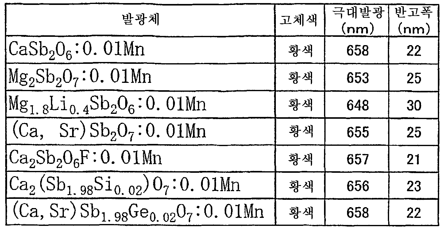
3) 본 발명에 의하면, 자외 또는 청색 발광을 매우 높은 연색성을 갖는 가시 백색 방사선으로 변환시키는 데 유용한 발광체는, 망간(IV)으로 부활된 안티몬산염도 포함한다. 이들 발광체는 약 600 내지 700 nm의 농적색 스펙트럼 영역에 있어서 발광대를 나타내거나, 또는 약 650 내지 660 nm의 좁은 구조화 발광을 나타낸다.3) According to the present invention, the light emitter useful for converting ultraviolet or blue light emission into visible white radiation having a very high color rendering property also includes an antimonate salt revived with manganese (IV). These emitters exhibit luminescent bands in the deep red spectral region of about 600 to 700 nm or narrow structured luminescence of about 650 to 660 nm.
이들 발광체는, 예를 들면These light emitting bodies are, for example
CaSb2O6: 0.01 Mn,CaSb 2 O 6 : 0.01 Mn,
Mg2Sb2O7: 0.01 Mn,Mg 2 Sb 2 0 7 : 0.01 Mn,
Mg1.8Li0.4Sb2O6: 0.01 Mn,Mg 1.8 Li 0.4 Sb 2 O 6 : 0.01 Mn,
삭제delete
(Ca, Sr)Sb2O7: 0.01 Mn,(Ca, Sr) Sb 2 O 7 : 0.01 Mn,
Ca2Sb2O6F: 0.01 Mn,Ca 2 Sb 2 O 6 F: 0.01 Mn,
Ca2(Sb1.98Si0.02)O7: 0.01 Mn,Ca 2 (Sb 1.98 Si 0.02 ) O 7 : 0.01 Mn,
(Ca, Sr)Sb1.98Ge0.02O7: 0.01 Mn이다.(Ca, Sr) Sb 1.98 Ge 0.02 O 7 : 0.01 Mn.
4) 자외 또는 청색 발광을 매우 높은 연색성을 갖는 가시 백색 방사선으로 변환시키기 위한 망간(IV) 부활 티탄산염을 포함하는 본 발명의 발광체는, 화학식 MeI xMeII yTi1-aO4Xm: Mnz로 표시된다.4) A light emitter of the present invention comprising manganese (IV) activated titanate for converting ultraviolet or blue light emission into visible white radiation having very high color rendering properties, has the formula Me I x Me II y Ti 1-a O 4 X m : Denoted by Mn z .
식 중, MeI은 Ca, Sr, Ba, Eu, Be, Mg 및 Zn으로 이루어지는 군으로부터 선택된 1종 이상의 2가 양이온이거나, 또는 주기율표 3족, 예를 들면 Sc, Y, La 및 Gd, Sm, Dy 및 Pr로부터 선택된 1종 이상의 3가 양이온이고, MeII는 알칼리 금속으로 이루어지는 군으로부터 선택된 1종 이상의 1가 양이온이다.Wherein Me I is at least one divalent cation selected from the group consisting of Ca, Sr, Ba, Eu, Be, Mg and Zn, or
식 중의 X는 전하의 균형을 잡기 위한 F 및 Cl로부터 선택된 이온이다.X in the formula is an ion selected from F and Cl to balance the charge.
0≤x≤4, 0≤y≤4, 0≤m≤4, 0≤a≤1, 0<z≤0.5이다.0 ≦ x ≦ 4, 0 ≦ y ≦ 4, 0 ≦ m ≦ 4, 0 ≦ a ≦ 1, and 0 <z ≦ 0.5.
Mn은 2 내지 4의 원자가로 격자에 들어가 있는 망간이다.Mn is manganese in the lattice at valences of 2-4.
티탄은 Zr, Hf, Si, Ge에 의해 완전히 또는 일부가 치환될 수도 있고, 일부가 B(붕소), Al(알루미늄), Ga(갈륨), In(인듐), P, Nb, Ta, V에 의해 치환될 수도 있으며, 이 경우 양이온 부분 격자에 있어서 적절한 전하 균형이 있거나, 또는 할로겐이 추가로 삽입되어 있다.Titanium may be completely or partially substituted by Zr, Hf, Si, Ge, and partly in B (boron), Al (aluminum), Ga (gallium), In (indium), P, Nb, Ta, V May be substituted, in which case there is an appropriate charge balance in the cationic partial lattice, or halogen is further inserted.
망간(IV) 부활 티탄산염을 포함하는 유용한 발광체는 Mg2TiO4, MgZnTiO4, Mg1.8Li0.4TiO4, MgBeTiO4, CaMgTiO4, Sr1.8Li0.2TiO4, Mg2Ti1.98Zr0.02O4, MgZnTi0.98Si0.02O4이다.Useful emitters comprising manganese (IV) reactivated titanates include Mg 2 TiO 4 , MgZnTiO 4 , Mg 1.8 Li 0.4 TiO 4 , MgBeTiO 4 , CaMgTiO 4 , Sr 1.8 Li 0.2 TiO 4 , Mg 2 Ti 1.98 Zr 0.02 O 4 , MgZnTi 0.98 Si 0.02 O 4 .
5) 본 발명에 의하면, 자외 또는 청색 발광을 매우 높은 연색성을 갖는 가시 백색 방사선으로 변환시키는 데 유용한 발광체에는 화학식 MeI xMeII yGe1-aOzXm: Mnw[식 중, MeI은 주기율표 2족 또는 3족으로부터 선택된 1종 이상의 2가 및(또는) 3가 금속 및(또는) Eu, Pr, Sm, Gd, Dy로 이루어지는 군으로부터 선택된 란타나이드 이온이고, MeII는 1종 이상의 1가 양이온이며, X는 Cl 원소 및 F 원소 중 1종 이상의 음이온임]로 표시되는 적색 발광 망간(IV) 부활 규산염-게르마늄산염을 포함하는 발광체도 포함된다. 5) According to the present invention, a light emitting body useful for converting ultraviolet or blue light emission into visible white radiation having a very high color rendering property includes a chemical formula Me I x Me II y Ge 1-a O z X m : Mn w where Me I is a lanthanide ion selected from the group consisting of at least one divalent and / or trivalent metal and / or Eu, Pr, Sm, Gd, Dy selected from
0≤w≤0.5, 0<x≤28, 0≤y≤14, 0≤m≤20, 0≤a<1, 0<z≤48이고, Ge는 Si, Zr, Ti에 의해 완전히 또는 일부가 치환될 수도 있고, 또는 일부가 B, Al, Ga, P, V, Nb, Ta, W, Mo에 의해 치환될 수도 있다.0≤w≤0.5, 0 <x≤28, 0≤y≤14, 0≤m≤20, 0≤a <1, 0 <z≤48, and Ge is completely or partially formed by Si, Zr, Ti It may be substituted, or a part may be substituted by B, Al, Ga, P, V, Nb, Ta, W, Mo.
이러한 발광체는These emitters
Ca2Si0.9Ge0.1O4: 0.005 Mn,Ca 2 Si 0.9 Ge 0.1 O 4 : 0.005 Mn,
Mg2Si0.5Ge0.5O4: 0.005 Mn,Mg 2 Si 0.5 Ge 0.5 O 4 : 0.005 Mn,
CaSrSi0.1Ge0.9O4: 0.003 Mn,CaSrSi 0.1 Ge 0.9 O 4 : 0.003 Mn,
MgZnSiO4: 0.003 Mn,MgZnSiO 4 : 0.003 Mn,
MgSiO3: 0.005 Mn,MgSiO 3 : 0.005 Mn,
CaMgSi0.95Ge0.05O4: 0.003 Mn,CaMgSi 0.95 Ge 0.05 O 4 : 0.003 Mn,
Mg28Ge9.45Si0.55O48: 0.005 Mn,Mg 28 Ge 9.45 Si 0.55 O 48 : 0.005 Mn,
Mg28Ge9SiO48: 0.005 Mn,Mg 28 Ge 9 SiO 48 : 0.005 Mn,
Mg28Ge7.2Si0.3O38F10: 0.003 Mn,Mg 28 Ge 7.2 Si 0.3 O 38 F 10 : 0.003 Mn,
Mg24Zn4Ge6.5SiO38F10: 0.005 Mn이다.Mg 24 Zn 4 Ge 6.5 SiO 38 F 10 : 0.005 Mn.
6) 본 발명에 의하면, 자외 또는 청색 발광을 매우 높은 연색성을 갖는 가시 백색 방사선으로 변환시키는 데 유용한 발광체에는, 588 nm 내지 610 nm의 광대역 발광 스펙트럼을 갖는 오렌지색 내지 오렌지색-적색 발광성 유로퓸 부활 규산염-게르마늄산염도 포함된다.6) According to the present invention, luminaries useful for converting ultraviolet or blue light emission into visible white radiation having very high color rendering properties include orange to orange-red luminescent europium activating silicate-germanium having a broadband emission spectrum of 588 nm to 610 nm. Acid salts are also included.
이들 발광체는, 예를 들면These light emitting bodies are, for example
Ca0.6Sr1.3Ba0.06Zn0.02Si0.9Ge0.1O4: 0.02 Eu,Ca 0.6 Sr 1.3 Ba 0.06 Zn 0.02 Si 0.9 Ge 0.1 O 4 : 0.02 Eu,
Ca0.6Sr1.2Ba0.1Zn0.08Si0.95Ge0.05O4: 0.02 Eu,Ca 0.6 Sr 1.2 Ba 0.1 Zn 0.08 Si 0.95 Ge 0.05 O 4 : 0.02 Eu,
Ca0.61Sr1.3Ba0.04Mg0.01Zn0.01Si0.97Ge0.03O4: 0.03 Eu,Ca 0.61 Sr 1.3 Ba 0.04 Mg 0.01 Zn 0.01 Si 0.97 Ge 0.03 O 4 : 0.03 Eu,
Ca0.8Sr0.11Ba0.04Be0.01Li0.1Si0.99Ge0.01O4: 0.03 Eu,Ca 0.8 Sr 0.11 Ba 0.04 Be 0.01 Li 0.1 Si 0.99 Ge 0.01 O 4 : 0.03 Eu,
Ca1.0Sr0.95Zn0.02Si0.95Ge0.05O4: 0.03 Eu,Ca 1.0 Sr 0.95 Zn 0.02 Si 0.95 Ge 0.05 O 4 : 0.03 Eu,
Ca0.9Sr0.9Ba0.08Mg0.05Zn0.05Ge0.45Si0.55O4: 0.02 Eu,Ca 0.9 Sr 0.9 Ba 0.08 Mg 0.05 Zn 0.05 Ge 0.45 Si 0.55 O 4 : 0.02 Eu,
Ca1.0Sr0.7Ba0.1Mg0.07Zn0.1Ge0.7Si0.3O4: 0.03 Eu,Ca 1.0 Sr 0.7 Ba 0.1 Mg 0.07 Zn 0.1 Ge 0.7 Si 0.3 O 4 : 0.03 Eu,
Ca0.65Sr1.28Ba0.02Li0.04Ge0.8Si0.2O4: 0.03 Eu,Ca 0.65 Sr 1.28 Ba 0.02 Li 0.04 Ge 0.8 Si 0.2 O 4 : 0.03 Eu,
Ca1.2Sr0.7Ba0.03Be0.05Ge0.05Si0.99O4: 0.02 Eu이다. Ca 1.2 Sr 0.7 Ba 0.03 Be 0.05 Ge 0.05 Si 0.99 O 4 : 0.02 Eu.
7) 본 발명에 의하면, 자외 또는 청색 발광을 매우 높은 연색성을 갖는 가시 백색 방사선으로 변환시키는 데 유용한 발광체에는, 육방 구조까지의 단순 스피넬형 구조를 갖는 화학식 MeI xMeII yAlmOn: Mn으로 표시되는 적색 발광성 망간(IV) 부활 알루민산염 또는 오렌지색 발광성 망간(II) 부활 알루민산염도 포함된다.7) According to the present invention, a light emitting body useful for converting ultraviolet or blue light emission into visible white radiation having a very high color rendering property includes a chemical formula Me I x Me II y Al m O n having a simple spinel structure up to a hexagonal structure: Also included are red luminescent manganese (IV) activated aluminate or orange luminescent manganese (II) activated aluminate represented by Mn.
식 중, MeI은 주기율표 2족 또는 3족으로부터 선택된 1종 이상의 원소 및(또는) Eu, Pr, Sm, Gd, Dy, Ce로 이루어지는 군으로부터 선택된 1종 이상의 란타나이드 이온이다. Wherein Me I is at least one element selected from
MeII는 1종 이상의 1가 양이온이다.Me II is at least one monovalent cation.
0≤x≤8, 0≤y≤4, 0<m≤16, 0<n≤27, 0<z≤0.5이다. 0 <x≤8, 0≤y≤4, 0 <m≤16, 0 <n≤27, and 0 <z≤0.5.
Al은 B 및(또는) Ga에 의해 완전히 또는 일부가 치환될 수도 있고, 일부가 P, V, Nb, Ta, Si, Ge, W, Mo에 의해 치환될 수도 있다.Al may be completely or partially substituted by B and / or Ga, and some may be substituted by P, V, Nb, Ta, Si, Ge, W, Mo.
이러한 발광체는 MgAl2O4, CaAl12O19, SrAl12O19, MgAl12O19, BeAl12O19, SrAl2O4, Sr0.5Mg0.5Al2O4, Sr4Al14O25, Mg2Al10O17, SrMgAl10O17, Sr2MgAl16O27, 2SrOㆍ3Al2O3, BaOㆍ4Al2O3 및 MgGa2O4이다. Such emitters include MgAl 2 O 4 , CaAl 12 O 19 , SrAl 12 O 19 , MgAl 12 O 19 , BeAl 12 O 19 , SrAl 2 O 4 , Sr 0.5 Mg 0.5 Al 2 O 4 , Sr 4 Al 14 O 25 , Mg 2 Al 10 O 17 , SrMgAl 10 O 17 , Sr 2 MgAl 16 O 27 , 2SrO.3Al 2 O 3 , BaO.4Al 2 O 3, and MgGa 2 O 4 .
8) 본 발명에 의하면, 자외 또는 청색 발광을 매우 높은 연색성을 갖는 가시 백색 방사선으로 변환시키는 데 유용한 발광체에는, 유로퓸-망간 이중 부활 발광체를 포함하는 발광체도 포함된다. 이 유로퓸-망간 이중 부활 발광체에 있어서, 1차 발광의 장파장 영역에서의 별개의 발광대 또는 숄더로서 황색 내지 적색에서 발생하는 망간(II) 이온의 발광을, 발광대가 망간(II) 중 하나 이상의 특징적인 여기대와 중첩되는 1차 부활제로 증감하여 Eu 발광이 청색 내지 녹색 스펙트럼 영역에서 발생한다.8) According to the present invention, the light emitting body useful for converting ultraviolet or blue light emission into visible white radiation having a very high color rendering property also includes a light emitting body comprising a europium-manganese double activating light emitting body. In this europium-manganese dual activating light emitting body, light emission of manganese (II) ions occurring in yellow to red as separate light emitting bands or shoulders in a long wavelength region of primary light emission is characterized by at least one of manganese (II) light emitting bands. Eu luminescence occurs in the blue to green spectral region by increasing and decreasing the primary activator overlapping with the normal excitation zone.
이들은 붕산염-규산염-인산염을 포함하고, 유로퓸 및 망간으로 부활되며, 화학식 MeI xMeII y(B, Si, P)aOnXm: Eu, Mn으로 표시되는 발광체이다.These include borate-silicate-phosphates and are revived with europium and manganese and are emitters represented by the formula Me I x Me II y (B, Si, P) a O n X m : Eu, Mn.
식 중, MeI은 주기율표 2족 및(또는) 3족으로부터 선택된 1종 이상의 원소 및(또는) Eu, Pr, Sm, Gd, Dy, Ce로 이루어지는 군으로부터 선택된 1종 이상의 란타나이드 이온이고, MeII는 1종 이상의 1가 양이온이며, X는 Cl, F, Br이다.Wherein Me I is at least one element selected from
0≤x≤10, 0≤y≤12, 0<a≤6, 0≤m≤16, 0<n≤24이고, B는 P, Si, Ga, Al에 의해 완전히 또는 일부가 치환될 수도 있으며, 일부가 V, Nb, Ta, Ge, W 및 Mo에 의해 치환될 수도 있다.0≤x≤10, 0≤y≤12, 0 <a≤6, 0≤m≤16, 0 <n≤24, B may be completely or partially substituted by P, Si, Ga, Al, , Part may be substituted by V, Nb, Ta, Ge, W and Mo.
사용되는 이러한 발광체는, 예를 들면Such emitters used are, for example,
SrBaP2O7: Eu, Mn,SrBaP 2 O 7 : Eu, Mn,
Sr2P1.68B0.32O7.84: Eu, Mn,Sr 2 P 1.68 B 0.32 O 7.84 : Eu, Mn,
Sr4Si3O8Cl4: Eu, Mn,Sr 4 Si 3 O 8 Cl 4 : Eu, Mn,
Ba3Mg(Si, P, Ge)2O8: Eu, Mn,Ba 3 Mg (Si, P, Ge) 2 O 8 : Eu, Mn,
(Sr, Ba)Al2Si2O8: Eu, Mn,(Sr, Ba) Al 2 Si 2 O 8 : Eu, Mn,
Sr10(PO4)6Cl2: Eu, Mn,Sr 10 (PO 4 ) 6 Cl 2 : Eu, Mn,
(Ba, Ca, Mg)10(PO4)6Cl2: Eu, Mn,(Ba, Ca, Mg) 10 (PO 4 ) 6 Cl 2 : Eu, Mn,
Ca3(PO4)2CaCl2: Eu, Mn,Ca 3 (PO 4 ) 2 CaCl 2 : Eu, Mn,
Ba1.3Sr0.75Ca0.75Mg0.9Zn0.1Si1.9Ge0.1O8: Eu, Mn,Ba 1.3 Sr 0.75 Ca 0.75 Mg 0.9 Zn 0.1 Si 1.9 Ge 0.1 O 8 : Eu, Mn,
Ba2.8MgSi1.8Ge0.2O8: Eu, Mn,Ba 2.8 MgSi 1.8 Ge 0.2 O 8 : Eu, Mn,
Sr2ZnSi1.6Ge0.4O7: Eu, Mn,Sr 2 ZnSi 1.6 Ge 0.4 O 7 : Eu, Mn,
Ba2Zn0.5Mg0.5Ge1.2Si0.8O7: Eu, Mn,Ba 2 Zn 0.5 Mg 0.5 Ge 1.2 Si 0.8 O 7 : Eu, Mn,
Ba3MgSi0.5Ge0.5O8: Eu, Mn,Ba 3 MgSi 0.5 Ge 0.5 O 8 : Eu, Mn,
BaZrO3: Eu, Mn,BaZrO 3 : Eu, Mn,
Ba3P2O8: Eu, Mn,Ba 3 P 2 O 8 : Eu, Mn,
α-Ca2P2O7: Eu, Mn,α-Ca 2 P 2 O 7 : Eu, Mn,
Ba5Ca3Si4O16: Eu, Mn,Ba 5 Ca 3 Si 4 O 16 : Eu, Mn,
Ba3SiO5: Eu, Mn이다. Ba 3 SiO 5 : Eu, Mn.
9) 신규한 발광체 또는 다른 발광대를 갖는 복수의 신규한 발광체는 발광 요소의 자외 또는 청색 발광을 연색 지수 Ra>90인 연색 Ia를 갖는 가시 백색 방사선으로 변환시키기 위한 혼합물에서의 성분으로서, 백색 발광 LED의 제조에서 사용함으로써 이들 LED를 본 발명에 의해 배경 조명 장치로서 사용할 수도 있고, 생활 공간 및 가구 조명, 사진 촬영 및 현미경 검사에 있어서, 의료 기술에 있어서, 박물관, 나아가 매우 진정한 연색이 중요한 어떠한 장소에서의 조명 기술에 있어서도 이용할 수 있다. 9) A plurality of novel light emitters with new light emitters or other light emitting bands are components in a mixture for converting the ultraviolet or blue light emission of a light emitting element into visible white radiation having color rendering index Ia having a color rendering index Ra> 90, wherein white light emission is present. By use in the manufacture of LEDs, these LEDs can also be used as background lighting devices according to the invention, and in living spaces and furniture lighting, photography and microscopy, in medical technology, museums and even any place where very true color rendering is important. It can be used also in the lighting technique.
(B) 본 발명의 다른 측면에 의해,(B) In another aspect of the present invention,
LED 소자로부터 방사되는 광에 기초하여 여기되어 여기광을 방사하는 발광체를 포함하는 파장 변환부를 갖는 광장치에 있어서,An optical device having a wavelength conversion portion including a light emitter that is excited based on light emitted from an LED element and emits excitation light,
상기 파장 변환부는 알칼리 토금속 안티몬산염의 고체계 및 고유 발광을 나타내는 이들로부터 유도된 계, 예를 들면 플루오로안티몬산염으로 형성된 발광 성분, 또는 망간(IV) 부활 안티몬산염, 티탄산염, 규산염-게르마늄산염 및 알루민산염으로 형성된 발광 성분, 또는 유로퓸 부활 규산염-게르마늄산염 또는 Eu(II) 및 2차 부활제로서의 Mn(II)로 이루어지는 군으로부터 선택된 증감제를 사용하고, 600 nm를 초과하는 스펙트럼 영역에서 오렌지색, 오렌지색-적색, 적색 또는 농적색을 나타내는 계로 형성된 발광 성분, 또는 다른 발광대를 가진 발광체를 포함하는 것을 특징으로 하는 광장치가 제공된다. The wavelength conversion portion is a light emitting component formed of a system derived from the solid-state and intrinsic luminescence of alkaline earth metal antimonate, for example, fluoroantimonate, or manganese (IV) -activated antimonate, titanate, silicate-germanate And a sensitizer selected from the group consisting of a luminescent component formed of aluminate, or europium-activated silicate-germanate or Eu (II) and Mn (II) as secondary activator, in the spectral region exceeding 600 nm. An optical device is provided which includes a light emitting component formed of a system exhibiting orange, orange-red, red or deep red, or a light emitting body having another light band.
(C) 본 발명의 다른 측면에 의해, (C) by another aspect of the present invention,
LED 소자, 상기 LED 소자를 탑재함과 동시에 LED 소자에 급전(給電)하기 위한 급전부, 상기 LED 소자와 급전부를 일체적으로 밀봉하는 광투과성을 갖는 밀봉부, 상기 LED 소자로부터 방사되는 광에 기초하여 여기되어 여기광을 방사하고, 알칼리 토금속 안티몬산염의 고체계 및 고유 발광을 나타내는 이들로부터 유도된 계, 예를 들면 플루오로안티몬산염으로 형성된 발광 성분, 또는 망간(IV) 부활 안티몬산염, 티탄산염, 규산염-게르마늄산염 및 알루민산염으로 형성된 발광 성분, 또는 유로퓸 부활 규산염-게르마늄산염 또는 Eu(II) 및 2차 부활제로서의 Mn(II)로 이루어지는 군으로부터 선택된 증감제를 사용하고, 600 nm를 초과하는 스펙트럼 영역에서 오렌지색, 오렌지색-적색, 적색 또는 농적색을 나타내는 계로 형성된 발광 성분, 또는 다른 발광대를 가진 발광체를 포함하는 파장 변환부를 갖는 것을 특징으로 하는 광장치가 제공된다.An LED element, a power supply portion for mounting the LED element and simultaneously supplying power to the LED element, a sealing portion having a light transmittance for integrally sealing the LED element and the power supply portion, and the light emitted from the LED element. Light-emitting components formed from those derived from these excited and radiated excitation light and exhibiting a solid system and intrinsic luminescence of alkaline earth metal antimonates, such as fluoroantimonates, or manganese (IV) -activated antimonates, 600 nm using a sensitizer selected from the group consisting of luminescent components formed from carbonates, silicates-germanates and aluminates, or europium-activated silicates-germanates or Eu (II) and Mn (II) as secondary activators Luminescent components formed by systems exhibiting orange, orange-red, red or deep red in the spectral region exceeding, or luminescence with other luminescent bands Square value, characterized in that it has a wavelength conversion portion including a is provided.
(D) 본 발명의 다른 측면에 의해, (D) According to another aspect of the present invention,
LED 램프, 상기 LED 램프로부터 방사되는 광을 도광(導光)하는 도광부, 상기 도광부를 통해 도광된 광에 기초하여 여기되어 여기광을 방사하고, 알칼리 토금속 안티몬산염의 고체계 및 고유 발광을 나타내는 이들로부터 유도된 계, 예를 들면 플루오로안티몬산염으로 형성된 발광 성분, 또는 망간(IV) 부활 안티몬산염, 티탄산염, 규산염-게르마늄산염 및 알루민산염으로 형성된 발광 성분, 또는 유로퓸 부활 규산염-게르마늄산염 또는 Eu(II) 및 2차 부활제로서의 Mn(II)로 이루어지는 군으로부터 선택된 증감제를 사용하고, 600 nm를 초과하는 스펙트럼 영역에서 오렌지색, 오렌지색-적색, 적색 또는 농적색을 나타내는 계로 형성된 발광 성분, 또는 다른 발광대를 가진 발광체를 포함하는 파장 변환부, 및 상기 파장 변환부를 통해 방사되는 광에 기초하여 조명되는 피조명부를 갖는 것을 특징으로 하는 광장치가 제공된다. An LED lamp, a light guiding part for guiding light emitted from the LED lamp, excited based on the light guided through the light guiding part to emit excitation light, and exhibiting a high system and intrinsic luminescence of alkaline earth metal antimonate Systems derived from these, for example luminescent components formed from fluoroantimonates, or luminescent components formed from manganese (IV) -activated antimonates, titanates, silicates-germanates and aluminates, or europium-activated silicates-germanates Or a luminescent component formed of a system exhibiting orange, orange-red, red or deep red in the spectral region exceeding 600 nm using a sensitizer selected from the group consisting of Eu (II) and Mn (II) as secondary activators Or a wavelength converter including a light emitter having a different light band, and based on light emitted through the wavelength converter. Square value comprising the blood illumination is provided.
도 1은 플루오로안티몬산 칼슘 발광체의 발광 스펙트럼이다.1 is an emission spectrum of a calcium fluoroantimonate emitter.
도 2는 피로안티몬산 칼슘 발광체의 발광 스펙트럼이다.2 is an emission spectrum of a calcium pyroantimonate emitter.
도 3은 Mg1.8Li0.4Sb2O6: 0.01 Mn(IV) 발광체의 발광 스펙트럼이다.3 is an emission spectrum of a Mg 1.8 Li 0.4 Sb 2 O 6 : 0.01 Mn (IV) emitter.
도 4는 티탄산 마그네슘: Mn(IV) 발광체의 발광 스펙트럼이다.4 is an emission spectrum of magnesium titanate: Mn (IV) emitter.
도 5는 Ca0.6Sr1.2Ba0.1Zn0.08Si0.95Ge0.05O4: 0.02 Eu 발광체의 발광 스펙트럼이다.5 is an emission spectrum of Ca 0.6 Sr 1.2 Ba 0.1 Zn 0.08 Si 0.95 Ge 0.05 O 4 : 0.02 Eu emitter.
도 6은 UVA 발광 1차 요소와의 조합에서의 발광체 혼합물의 발광 스펙트럼(색 온도 9700 K, Ra=98)이다.FIG. 6 is the emission spectrum (
도 7은 UVA 발광 1차 요소와의 조합에서의 발광체 혼합물의 발광 스펙트럼(색 온도 6500 K, Ra=99)이다.FIG. 7 is the emission spectrum (
도 8은 UVA 발광 1차 요소와의 조합에서의 발광체 혼합물의 발광 스펙트럼(색 온도 5400 K, Ra=99)이다.FIG. 8 is the emission spectrum (color temperature 5400 K, Ra = 99) of the luminescent mixture in combination with the UVA luminescent primary element.
도 9는 UVA 발광 1차 요소와의 조합에서의 발광체 혼합물의 발광 스펙트럼(색 온도 4100 K, Ra=99)이다.9 is the emission spectrum (
도 10은 UVA 발광 1차 요소와의 조합에서의 발광체 혼합물의 발광 스펙트럼(색 온도 2870 K, Ra=99)이다.10 is the emission spectrum (
도 11은 UVA 발광 1차 요소와의 조합에서의 발광체 혼합물의 발광 스펙트럼(색 온도 2250 K, Ra=99)이다. FIG. 11 is the emission spectrum (
도 12는 청색 발광 LED와, 색 온도 6500 K, Ra=95의 본 발명에 의한 발광체 혼합물을 조합한 백색 발광 LED의 발광 스펙트럼이다.12 is an emission spectrum of a white light emitting LED combining a blue light emitting LED and a light emitting mixture according to the present invention having a color temperature of 6500 K and Ra = 95.
도 13은 제1 실시 형태의 발광 장치를 나타내는 단면도이다.13 is a cross-sectional view showing the light emitting device of the first embodiment.
도 14는 제1 실시 형태의 LED 소자의 층 구성도이다.It is a layer block diagram of the LED element of 1st Embodiment.
도 15는 제1 실시 형태의 LED 소자의 다른 구성을 나타내는 층 구성도이다.It is a layer block diagram which shows the other structure of the LED element of 1st Embodiment.
도 16은 제2 실시 형태의 발광 장치를 나타내며, (a)는 종단면도, (b)는 LED 소자의 부분 확대도이다.Fig. 16 shows the light emitting device of the second embodiment, (a) is a longitudinal sectional view, and (b) is a partial enlarged view of the LED element.
도 17은 제3 실시 형태의 발광 장치를 나타내는 단면도이다.17 is a cross-sectional view illustrating the light emitting device of the third embodiment.
도 18은 제4 실시 형태의 발광 장치를 나타내는 단면도이다.18 is a cross-sectional view showing a light emitting device of a fourth embodiment.
도 19는 제5 실시 형태의 발광 장치를 나타내는 단면도이다.19 is a cross-sectional view showing a light emitting device of a fifth embodiment.
도 20은 제6 실시 형태의 발광 장치를 나타내는 단면도이다.20 is a cross-sectional view showing a light emitting device of a sixth embodiment.
도 21은 제7 실시 형태의 광장치로서의 액정 백 라이트 장치를 나타내는 단면도이다.21 is a cross-sectional view showing a liquid crystal backlight device as an optical device according to a seventh embodiment.
<발명을 실시하기 위한 최선의 형태>Best Mode for Carrying Out the Invention
이하, 본 발명의 발광체 및 이것을 이용한 광장치에 대하여 도면 등을 참조하여 상세하게 설명한다.EMBODIMENT OF THE INVENTION Hereinafter, the light emitting body of this invention and the optical device using the same are demonstrated in detail with reference to drawings.
우선, LED 또는 다른 1차 발광 요소에 있어서 자외 및 청색 방사선을 높은 연색성을 갖는 가시 백색 방사선으로 변환시키는 발광체의 제조에 대하여 설명한다.First, the production of a luminous body for converting ultraviolet and blue radiation into visible white radiation having high color rendering in an LED or other primary light emitting element will be described.
알칼리 토금속 안티몬산염:Alkaline Earth Metal Antimonate:
알칼리 토금속 안티몬산염은 열분해에 의해 금속 산화물을 형성하는 산화물, 탄산염 또는 다른 화합물, 및 적절한 금속의 할로겐화물로 제조된다.Alkaline earth metal antimonates are prepared from oxides, carbonates or other compounds that form metal oxides by pyrolysis, and halides of suitable metals.
또한, 다른 안티몬산염 발광체의 대표예로서, 양이온으로서 칼슘을 갖는 염기성 화합물인 메타안티몬산 칼슘, 피로안티몬산 칼슘 및 플루오로안티몬산 칼슘의 제조를 설명한다.Further, as representative examples of other antimonate light emitters, the production of calcium metaantimonate, calcium pyroantimonate and calcium fluoroantimonate, which are basic compounds having calcium as cations, will be described.
메타안티몬산 칼슘 CaSb2O6을 사산화안티몬 및 탄산칼슘으로부터, 공기 또는 질소 50 %, 산소 50 %를 포함하는 산화성 분위기하에 2 단계로 하소함으로써 제조한다. 2 단계 하소는 화학양론량의 원료 혼합물을 985 ℃에서 1 시간 하소한 후, 균질화 중간체를 1200 ℃에서 8 시간 하소함으로써 행해진다. 이 반응은 하기 반응식에 따라 진행된다.Calcium metaantimonate CaSb 2 O 6 is prepared by calcination from antimony tetraoxide and calcium carbonate in two stages under an oxidizing atmosphere containing air or 50% nitrogen and 50% oxygen. Two-step calcination is performed by calcining the stoichiometric amount of the raw material mixture at 985 ° C. for 1 hour and then calcining the homogenizing intermediate at 1200 ° C. for 8 hours. This reaction proceeds according to the following scheme.
Sb2O4+CaCO3+1/2O2 → CaSb2O6+CO2 Sb 2 O 4 + CaCO 3 + 1 / 2O 2 → CaSb 2 O 6 + CO 2
그 후, 얻어진 생성물을 분쇄하고, 세정하여 미전화 산화물을 용해 제거한다. 건조 및 체 분류 후의 발광체는 약간 황색을 띤 색을 갖는다.Thereafter, the obtained product is ground and washed to dissolve and remove the unconverted oxide. The light emitter after drying and sifting has a slightly yellowish color.
상기 반응식에 의한 탄산칼슘의 양을 2배로 한 것 이외에는, 동일한 조건하에서 피로안티몬산 칼슘 Ca2Sb2O7을 합성한다.Calcium pyroantimonate Ca 2 Sb 2 O 7 is synthesized under the same conditions except that the amount of calcium carbonate is doubled.
제1 하소를 975 ℃에서 실시하고, 제2 하소를 1175 ℃에서 실시하는 것 이외에는, 동일한 방법으로 플루오로안티몬산 칼슘 Ca2Sb2O6F2를 합성한다. 반응식을 간략화한 것을 이하에 나타낸다.Calcium fluoroantimonate Ca 2 Sb 2 O 6 F 2 is synthesized in the same manner except that the first calcination is performed at 975 ° C. and the second calcination is performed at 1175 ° C. A simplified scheme is shown below.
2Sb2O4+3CaCO3+CaF2+1/2O2 → 2Ca2Sb2O6F+3CO2 2Sb 2 O 4 + 3CaCO 3 + CaF 2 + 1 / 2O 2 → 2Ca 2 Sb 2 O 6 F + 3CO 2
그 후, 메타안티몬산 칼슘 및 피로안티몬산 칼슘이 사방 격자로 결정화되고, 플루오로안티몬산 칼슘이 AIA(JECS110(1963)1048)와 일치한 변형된 피로클로어 구조를 갖는다.Thereafter, the calcium metaantimonate and calcium pyroantimonate crystallized in a tetragonal lattice, and the calcium fluoroantimonate has a modified pyrochlore structure consistent with AIA (JECS 110 (1963) 1048).
합성된 안티몬산염 및 플루오로안티몬산염은 반고폭이 약 100 nm 내지 150 nm에서 약 620 nm 내지 670 nm의 극대치를 갖는 적색 스펙트럼 영역 내의 광대역 발광을 나타낸다.The synthesized antimonates and fluoroantimonates exhibit broadband luminescence in the red spectral region, with semi-high widths of about 100 nm to 150 nm and maximums of about 620 nm to 670 nm.
도 1은 플루오로안티몬산 칼슘 발광체의 발광 스펙트럼을 나타낸다. 도 2는 피로안티몬산 칼슘 발광체의 발광 스펙트럼을 재현한 것이다.1 shows the emission spectrum of calcium fluoroantimonate emitter. 2 is a reproduction of the emission spectrum of the calcium pyroantimonate emitter.
기본적으로는 안티몬의 일부가 다른 5가 원소, 예를 들면 V, Nb, Ta, P, As 및 Bi에 의해 문제없이 교환될 수 있으며, 반응 조건은 변경하지 않고 그 상태이다. 해당 원소를 이들의 산화물 형태나, 또는 열분해에 의해 산화물을 형성하는 화합물 형태로 첨가한다.Basically, some of the antimony can be exchanged without problems by other pentavalent elements such as V, Nb, Ta, P, As and Bi, and the reaction conditions remain unchanged. The element is added in the form of oxides thereof or in the form of compounds which form oxides by pyrolysis.
4가의 산형성제, 예를 들면 Ti, Zr, Hf, Si, Ge를 함유시키는 경우, 1가의 금속 이온을 동시에 첨가함으로써 전하 균형이 이루어지고, Mo 및 W를 함유시키는 경우, 3가 양이온을 첨가하는 것이 유리한 경우가 있다.In the case of containing a tetravalent acid forming agent, for example, Ti, Zr, Hf, Si, Ge, charge balance is achieved by simultaneously adding monovalent metal ions, and in the case of containing Mo and W, a trivalent cation is added. It is sometimes advantageous.
또한, 3가 양이온을 사용하는 경우, 1가 금속 이온 또는 추가의 할로겐 원자에 의한 전하 균형이 있다는 점에 주의해야 한다.It should also be noted that when using trivalent cations, there is a charge balance by monovalent metal ions or additional halogen atoms.
하기 표 1에 안티몬산염 발광체의 발광 특성을 나타낸다. Table 1 shows the light emission characteristics of the antimonate light emitter.

부활제로서 망간(IV)를 갖는 발광체:Light emitter with manganese (IV) as activator:
적색 발광 Mn(IV) 부활 발광체계는, 마찬가지로 백색 LED에서의 본 발명에 의한 용도 및 배경 조명 장치에 있어서, 생활 공간 및 가구 조명에 있어서, 사진 촬영 및 현미경 검사에 있어서, 의료 기술에 있어서, 박물관에서의 조명 기술, 나아가 진정한 연색이 요구되는 어떠한 장소에 있어서든 바람직하다.The red light emitting Mn (IV) revive light emitting system is similarly used in the white LED in the LED and in the backlighting device, in living space and furniture lighting, in photography and microscopy, in medical technology, in museums It is desirable in any place where lighting technology in Esau, even true color rendering, is required.
제조 및 식이 이미 설명된 매트릭스로서의 안티몬산염 외에 티탄산염, 규산염-게르마늄산염 및 알루민산염을 포함하는 적색 발광 Mn(IV) 부활 발광체계도, 자외 또는 청색 발광을 매우 높은 연색성을 갖는 가시 백색 방사선으로 변환시키는 데 바람직하다.Red-emitting Mn (IV) activated luminescent systems comprising titanates, silicates-germanates and aluminates, in addition to antimonates as the matrix already described and formulated, also convert ultraviolet or blue luminescence into visible white radiation with very high color rendering properties. It is preferable to convert.
모든 망간(IV) 부활 발광체를 제조하면 원료, 예를 들면 산화물, 탄산염 및 할로겐화물, 나아가 산화망간(IV)를 혼합하고, 이어서 공기 중 또는 산소 중에 1200 ℃를 초과하는 고온에서 몇시간 하소한다. 중간체를 완전히 균질화한 후에 2차 하소 공정을 행함으로써, 얻어지는 생성물의 품질이 높아지고, 모두가 황색을 띤 백색 내지 황색을 띤 녹색을 가지며, 즉 장파장 UV 방사선 또는 청색광을 흡수한다. 이어지는 공정, 예를 들면 하소 케이크의 분쇄, 세정 및 체 분류를 기존의 발광체의 제조와 동일하게 실시한다.When all manganese (IV) activated luminescent materials are prepared, raw materials such as oxides, carbonates and halides, and further manganese (IV), are mixed and then calcined for several hours at temperatures above 1200 ° C. in air or oxygen. By carrying out the secondary calcination process after fully homogenizing the intermediate, the quality of the product obtained is high and all have yellowish white to yellowish green color, i.e. absorb long wavelength UV radiation or blue light. Subsequent processes, for example, calcination, rinsing and sifting of the calcined cake, are carried out in the same manner as in the production of conventional light emitting bodies.
모든 망간(IV) 부활 발광체는 약 620 nm 내지 700 nm의 적색 스펙트럼 영역에서 발광대를 나타내거나, 약 650 내지 660 nm의 좁은 구조화 발광을 나타낸다.All manganese (IV) activated emitters exhibit luminescent bands in the red spectral region of about 620 nm to 700 nm or narrow structured emission of about 650 to 660 nm.
하기 표 2에 몇가지 선택된 발광체의 예를 이용한 망간(IV) 부활 안티몬산염의 발광 특성을 나타낸다.Table 2 below shows the luminescence properties of manganese (IV) -activated antimonate using several selected emitters.
망간(IV) 부활 티탄산염의 발광체를 하기 표 3에 나타낸다. 발광체의 발광치는 완전 산화성 하소를 적용함으로써 얻을 수 있다.The emitter of manganese (IV) activated titanate is shown in Table 3 below. The luminous value of the luminous body can be obtained by applying complete oxidative calcination.

불완전 산화의 경우, 보다 단파장으로 변이한 발광체에 있어서, 상이하거나 또는 추가의 발광대를 얻을 수 있다. 이들은 마찬가지로 백색 발광 성분의 제조에 사용할 수 있다.In the case of incomplete oxidation, different or additional light emission bands can be obtained for light-emitting bodies which are shorter in wavelength. These can likewise be used for the production of white light emitting components.
망간(IV) 부활 규산염-게르마늄산염 발광체 및 이들의 특성을 하기 표 4에 나타낸다.Manganese (IV) activated silicate-germanate emitters and their properties are shown in Table 4 below.

본 발명에 의하면, 광대역 오렌지색 내지 오렌지색-적색 발광대를 나타내는 규산염-게르마늄산염을 포함하는 발광체를, 칼슘, 및 추가로 망간 부활이 불필요한 경우 및 망간 대신에 유로퓸을 부활제로서 함유시키는 경우에는 보다 작은 양이온을 함유하는 3원 화합물을 사용하여 제조할 수 있다. 이들을 LED에 사용하면, 연색 지수 Ra>95를 갖는 매우 높은 연색성을 얻을 수 있다.According to the present invention, a light-emitting body including a silicate-germanate having a broad band orange to orange-red light emission band has a smaller size when calcium and manganese activation are unnecessary and when europium is contained as an activator instead of manganese. It can be prepared using a ternary compound containing a cation. When used in LEDs, very high color rendering properties with color rendering index Ra> 95 can be obtained.
이하의 반응식에 따라, 대응하는 금속 산화물 및 탄산염으로부터 N2/H2=9:1인 환원 분위기 중에 온도 1200 ℃ 내지 1300 ℃에서 3 내지 5 시간 고체 반응을 행함으로써 유로퓸(II) 부활 규산염-게르마늄산염을 제조한다:According to the following reaction formula, Europium (II) -activated silicate-germanium was subjected to solid reaction at a temperature of 1200 ° C. to 1300 ° C. for 3 to 5 hours in a reducing atmosphere having N 2 / H 2 = 9: 1 from corresponding metal oxides and carbonates. Prepares Acids:
CaCO3+SrCO3+SiO2+GeO2+Eu2O3 → (Ca, Sr, Ba, Eu)2(Si, Ge)O4+2CO2 CaCO 3 + SrCO 3 + SiO 2 + GeO 2 + Eu 2 O 3 → (Ca, Sr, Ba, Eu) 2 (Si, Ge) O 4 + 2CO 2
얻어지는 조(粗) 발광체를 세정하고 체 분류한다. 얻어진 발광체는 사방 구조를 갖는다.The crude light emitter obtained is washed and sifted. The obtained light emitter has a tetragonal structure.
유로퓸(II) 부활 규산염-게르마늄산염 발광체 및 이들의 발광 특성을 하기 표 5에 나타낸다.Europium (II) -activated silicate-germanate emitters and their luminescent properties are shown in Table 5 below.

망간(IV) 부활 알루민산염 발광체:Manganese (IV) Revitalizing Aluminate Light Emitters:
알루민산염이 마그네토플럼바이트 구조 또는 다른 육방 구조를 갖는 한, 단순 스피넬로부터 적색 또는 오렌지색 발광계를 효율적으로 얻을 수 있는 가능성이 있다. 불완전 산화의 경우, 마찬가지로 발광이 보다 단파장에서 발생하는 경우의 LED에서의 방사선 변환제로서 사용할 수 있는 발광체가 형성된다.As long as the aluminate has a magneto plumbite structure or other hexagonal structure, there is a possibility of efficiently obtaining a red or orange luminescence system from a simple spinel. In the case of incomplete oxidation, a light-emitting body that can be used as a radiation converting agent in an LED in the case where light emission occurs at a shorter wavelength is likewise formed.
하기 표 6에 몇가지 망간(IV) 부활 알루민산염 발광체 및 이들의 발광 특성을 나타낸다. Table 6 below shows some manganese (IV) activated aluminate emitters and their luminescent properties.

유로퓸-망간 이중 부활 발광체:Europium-manganese double resurrection luminaries:
1차 발광의 장파장 영역에서의 별개의 발광대 또는 숄더로서 황색 내지 적색을 발생시키는 망간(II) 이온의 발광은, 발광대가 망간(II) 중 하나 이상의 특징적인 여기대와 중첩되는 1차 부활제에 의해 증감할 필요가 있다. 즉, Eu 발광은 청색 내지 청색-녹색 스펙트럼 영역이 되어야 한다. LED에 종래에는 사용되지 않았던 이하의 화합물을 본 발명에 의해 합성하였다. 이들 화합물 전부는 본 발명에 의해 선택되는 조성물에 따라 청색 내지 녹색 성분으로서 사용할 수도 있다.The emission of manganese (II) ions, which generate yellow to red as separate light emitting bands or shoulders in the long wavelength region of the primary light emission, is a primary activator in which the light emitting band overlaps the characteristic excitation band of one or more of manganese (II). It is necessary to increase and decrease by. In other words, Eu emission should be in the blue to blue-green spectral region. The following compounds which were not conventionally used for LEDs were synthesized by the present invention. All of these compounds may be used as blue to green components depending on the composition selected by the present invention.
유로퓸과 망간으로 부활한 붕산염-규산염-인산염을 포함하는 발광체 및 이들의 발광 특성을 하기 표 7에 나타낸다.Light emitters comprising borate-silicate-phosphate revived with europium and manganese and their luminescent properties are shown in Table 7 below.

본 발명에 의한 발광체에 의해 발광체 혼합물을 얻을 수 있다. 이들 발광체 혼합물에 의하면, 380 nm 내지 780 nm의 범위에서 8종 이하의 개개의 스펙트럼을 중첩시킴으로써 가시광선 범위에서 연속된 스펙트럼을 갖는 백색 LED를 제조할 수 있다.The light-emitting body mixture can be obtained by the light-emitting body according to the present invention. According to these light-emitting mixtures, white LEDs having a continuous spectrum in the visible range can be produced by superimposing up to eight individual spectra in the range of 380 nm to 780 nm.
이에 따라 색 온도가 약 10000 K 내지 2000 K이고, 연색 지수 Ra가 99인 주광 내지 온백색광의 여러종의 광을 실현할 수 있다.Thereby, various kinds of light from daylight to warm white light having a color temperature of about 10000 K to 2000 K and a color rendering index Ra of 99 can be realized.
본 발명에 의한 발광체 혼합물을 사용한 몇가지 백색 LED의 발광 스펙트럼을 도 6 내지 도 12에 나타내었다.The emission spectra of several white LEDs using the phosphor mixture according to the invention are shown in FIGS.
(본 발명의 발광체의 효과)(Effect of Light Emitting Device of the Present Invention)
(1) 본 발명에 의한 발광체를 백색 발광 구성 요소의 제조에 사용하는 것은, 개개의 성분의 고유 흡수를 고려하면서, 발광체의 개개의 발광 스펙트럼을 통상의 자외 또는 청색 발광 구성 요소의 1차 스펙트럼과 혼합하는 것을 규정한 것을 기초로 하고 있다. 청색 또는 UV 발광 구성 요소에 사용하면, 본 발명에 의한 발광체 및 이들의 혼합물에 의해 매우 효율적으로 자연광 또는 백열 램프광에 가까운 스펙트럼을 갖는 질적으로 신규한 백색광을 얻을 수 있다. 이러한 백색 발광 조명 요소는 바람직하게는 연색 Ia가 중요할 뿐만 아니라, 보여지는 느낌이 자연광, 백열 램프광 또는 할로겐 램프광하에서의 것에 가까운 연색성도 중요시되는 경우에 사용된다.(1) The use of the light emitter according to the present invention for the production of white light emitting components is characterized by the fact that the individual light emission spectra of the light emitters are combined with the primary spectrum of a conventional ultraviolet or blue light emitting component, taking into account the intrinsic absorption of the individual components. It is based on the thing specified to mix. When used in a blue or UV light emitting component, the luminescent material and mixtures thereof according to the invention can very efficiently obtain qualitatively novel white light with a spectrum close to natural or incandescent lamp light. Such white light emitting illumination elements are preferably used when not only the color rendering Ia is important, but also color rendering close to that under natural light, incandescent lamp light or halogen lamp light.
(2) LED 또는 다른 1차 발광 요소에 있어서, 자외 및 청색 방사선을 높은 연색성의 가시 백색 방사선으로 변환시키기 위해, 본 발명에 의하면 오렌지색-적색 또는 적색 스펙트럼 영역에서의 광대역 발광, 또는 650 nm 초과의 농적색 스펙트럼 영역에서의 보다 좁은 대역의 발광을 나타내는 발광체를 사용한다. 본 발명에 의한 오렌지색 성분 및 적색 성분을 사용한 8종 이하의 발광체 성분을 포함하고, 색파장 380 nm 내지 780 nm의 넓은 발광 연속 상태를 나타내는 발광체 혼합물도 자외 및 청색 방사선을 가시 백색 방사선으로 변환시키는 데 적당하다.(2) In the LED or other primary light emitting element, in order to convert ultraviolet and blue radiation into high color rendering visible white radiation, according to the present invention broadband emission in the orange-red or red spectral region, or greater than 650 nm Light emitters showing narrower bands of emission in the deep red spectral region are used. A light-emitting mixture comprising up to 8 light-emitting components using an orange component and a red component according to the present invention, and exhibiting a wide emission continuous state of color wavelengths from 380 nm to 780 nm, is also used to convert ultraviolet and blue radiation into visible white radiation. It is suitable.
(3) 광대역 오렌지색-적색 또는 적색 스펙트럼 영역, 또는 농적색의 보다 좁은 스펙트럼 영역에 매우 바람직한 발광체에 알칼리 토금속 안티몬산염의 고체계, 및 이들로부터 유도된 계, 예를 들면 고유 발광을 나타내거나, 망간(IV) 또는 티탄(IV)으로 부활한 플루오로안티몬산염이 있다. (3) exhibit a solid system of alkaline earth metal antimonate, and a system derived therefrom, for example intrinsic luminescence, or Fluoroantimonates that are revived with (IV) or titanium (IV).
(4) Eu(II)로 이루어지는 군으로부터 선택된 증감제 및 2차 부활제로서의 Mn(II)를 사용한 계에 의해 지속적인 가능성이 시사된다.(4) Sustainability is suggested by the system using Mn (II) as a sensitizer selected from the group consisting of Eu (II) and a secondary activator.
이하, 상기 발광체를 이용한 광장치를 상세하게 설명한다.Hereinafter, the square value using the said light-emitting body is demonstrated in detail.
<제1 실시 형태><First Embodiment>
도 13은 본 발명의 제1 실시 형태의 발광 장치를 나타내는 단면도이다.13 is a cross-sectional view showing a light emitting device of the first embodiment of the present invention.
이 발광 장치 (1)은 LED 소자를 리드에 탑재한 파장 변환형 발광 장치 (1)이며, 배선 도체인 리드 (2) 및 (3), 리드 (2)에 설치되는 LED 소자 수용용 컵부(cup 部) (4), 컵부 (4)의 바닥부 (5)에 접착된 LED 소자 (6), LED 소자 (6)의 도시하지 않은 전극과 리드 (2) 및 (3)을 전기적으로 접속하는 Au를 포함하는 와이어 (7), LED 소자 (6) 및 와이어 (7)과 함께 컵부 (4)를 밀봉하는 광투과성 밀봉 수지 (8), 밀봉 수지 (8)에 혼합되는 발광체 (9), 및 광투과성을 갖고 리드 (2) 및 (3)과 LED 소자 (6)과 와이어 (7)을 일체적으로 밀봉하는 포탄 형상의 밀봉 수지 (10)을 갖는 다.This
리드 (2) 및 (3)은 열전도성 및 도전성이 우수한 구리 또는 구리 합금에 의해 형성되며, 리드 (3)에 설치되는 컵부 (4)는 컵 외부에의 광방사성을 높이기 위해 내벽의 광출사측을 확대함으로써 경사를 갖는다.The leads 2 and 3 are formed of copper or a copper alloy excellent in thermal conductivity and conductivity, and the
LED 소자 (6)은 파장 460 nm의 청색광을 방사하는 GaN계 LED 소자이며, 컵부 (4)의 바닥부 (5)에 광반사성을 갖는 접착재에 의해 접착 고정되어 있다.The
밀봉 수지 (8)은 발광체 (9)가 혼합된 실리콘 수지이며, 컵부 (4)에 포팅 주입됨으로써 LED 소자 (6)을 밀봉하고 있다.The sealing
발광체 (9)는 알칼리 토금속 안티몬산염의 고체계 및 고유 발광을 나타내는 이들로부터 유도된 계, 예를 들면 플루오로안티몬산염으로 형성된 발광 성분, 또는 망간(IV) 부활 안티몬산염, 티탄산염, 규산염-게르마늄산염 및 알루민산염으로 형성된 발광 성분, 또는 유로퓸 부활 규산염-게르마늄산염 또는 Eu(II) 및 2차 부활제로서의 Mn(II)로 이루어지는 군으로부터 선택된 증감제를 사용하고, 600 nm를 초과하는 스펙트럼 영역에서 오렌지색, 오렌지색-적색, 적색 또는 농적색을 나타내는 계로 형성된 발광 성분, 또는 다른 발광대를 가지며, 이들의 중첩에 의해 청색-백색을 갖는 약 10000 K 내지 주광색을 갖는 6500 K의 색 온도, 및 온백색을 갖는 약 3000 K의 색 온도 내지 적색을 띤 황색의 저녁 광색을 갖는 2000 K의 색 온도를 갖는 약 380 nm 내지 780 nm 사이의 넓은 발광 연속 상태를 형성하는, 8종 이하의 발광체 성분의 혼합물로 형성된 발광 성분을 포함하는 것을 사용한다.The
구체적으로, 밀봉 수지 (8)에는 화학식 MeI xMeII ySba0bXc[식 중, MeI은 칼슘(Ca), 스트론튬(Sr), 바륨(Ba), 카드뮴(Cd), 아연(Zn), 베릴륨(Be), 마그네슘(Mg), 유로퓸(Eu), 망간(Mn), 스칸듐(Sc), 이트륨(Y), 란탄(La), 사마륨(Sm), 프라세오디뮴(Pr), 디스피로슘(Dy), 테르븀(Tb)으로 이루어지는 군으로부터 선택된 1종 이상의 원소이고, MeII는 리튬(Li), 나트륨(Na), 칼륨(K), 루비듐(Rb), 세슘(Cs)으로 이루어지는 군으로부터 선택된 1종 이상의 원소이며, X(대문자)는 불소(F), 염소(Cl), 브롬(Br)으로 이루어지는 군으로부터 선택된 1종 이상의 원소이고, x(소문자)는 0 내지 8이며, y는 0 내지 4이고, 0<a<16, 0<b<64, 0≤c≤4이며, 안티몬(Sb)이 바나듐(V), 니오븀(Nb), 탄탈륨(Ta), 인(P), 비소(As), 티탄(Ti), 지르코늄(Zr), 하프늄(Hf), 규소(Si), 게르마늄(Ge), 몰리브덴(Mo), 텅스텐(W)에 의해 일부가 치환될 수도 있고, 또는 이들로부터 유도되는 계, 예를 들면 플루오로안티몬산염을 포함할 수도 있음]로 표시되는 발광성 알칼리 토금속 안티몬산염을 포함하는 발광체 (9)가 혼합되어 있다.Specifically, the sealing resin (8) has the formula Me I x Me II y Sb a 0 b X c [wherein, Me I is calcium (Ca), strontium (Sr), barium (Ba), cadmium (Cd), zinc (Zn), beryllium (Be), magnesium (Mg), europium (Eu), manganese (Mn), scandium (Sc), yttrium (Y), lanthanum (La), samarium (Sm), praseodymium (Pr), dis At least one element selected from the group consisting of pyrosium (Dy) and terbium (Tb), and Me II consists of lithium (Li), sodium (Na), potassium (K), rubidium (Rb), and cesium (Cs) At least one element selected from the group, X (uppercase) is at least one element selected from the group consisting of fluorine (F), chlorine (Cl), bromine (Br), x (lowercase) is 0 to 8, y Is 0 to 4, 0 <a <16, 0 <b <64, 0≤c≤4, and antimony (Sb) is vanadium (V), niobium (Nb), tantalum (Ta), phosphorus (P), Partial substitution by arsenic (As), titanium (Ti), zirconium (Zr), hafnium (Hf), silicon (Si), germanium (Ge), molybdenum (Mo), tungsten (W) Or a system derived from them, for example, may include a fluoroantimonate].
밀봉 수지 (10)은 에폭시 수지를 포함하며, 포탄 형상을 형성하기 위한 틀을 이용한 캐스팅 몰딩법에 의해 광출사측에 반구상의 광학 형상을 갖고 있다.The sealing
도 14는 LED 소자 (6)의 층 구성도이다. LED 소자 (6)은 사파이어 기판 (61), 사파이어 기판 (61) 상에 형성되는 AlN 완충층 (62), AlN 완충층 (62) 상에 형성되는 Si 도핑의 n형 GaN 피복층(컨택트층) (63), n형 GaN 피복층 (63) 상에 3층의 InGaN 웰층 (64A)와 2층의 GaN 장벽층 (64B)를 교대로 배치하여 형성되는 MQW (64), MQW (64) 상에 형성되는 Mg 도핑의 p형 GaN 피복층 (65), p형 GaN 피복층 (65) 상에 형성되는 Mg 도핑의 p형 GaN 컨택트층 (66), p형 GaN 컨택트층 (66) 상에 형성되는 투명 전극 (67), 투명 전극 (67) 상의 소정의 위치, 예를 들면 소자 측면 근처에 형성되는 패드 전극 (68)과, 에칭에 의해 p형 GaN 컨택트층 (66), p형 GaN 피복층 (65), MQW (64), 및 n형 GaN 피복층 (63)의 일부를 제거함으로써 노출된 n형 GaN 피복층 (63)에 형성되는 n측 전극 (69)를 갖는다. 이 LED 소자 (6)은 발광층으로서 MQW (64)를 갖는 더블 헤테로 구조를 갖고 있으며, 각 층에 적절하게 Al을 포함하는 구성으로 할 수도 있다.14 is a layer configuration diagram of the
이어서, 발광 장치 (1)의 제조 방법에 대하여 설명한다.Next, the manufacturing method of the
우선, 리드 프레임이 되는 구리판을 가압 가공에 의해 펀칭함으로써 리드 (2) 및 (3)을 갖는 리드 프레임을 형성한다. 또한, 리드 프레임의 형성시에 컵부 (4)를 리드 (3)에 형성한다. 이어서, 컵부 (4) 내에 LED 소자 (6)을 접착재로 접착 고정한다. 이어서, LED 소자 (6)의 패드 전극 (68)과 리드 (2), 및 n측 전극 (69)와 리드 (3)을 와이어 (7)로 전기적으로 접속한다. 이어서, 미리 발광체 (9)를 혼합한 실리콘 수지를 컵부 (4)에 포팅 주입함으로써 LED 소자 (6)을 밀봉한다. 이어서, 수지 성형용 틀에 LED 소자 (6)이 밀봉된 리드 (2) 및 (3)을 삽입한다. 이어서, 틀 내에 에폭시 수지를 주입함으로써 리드 (2) 및 (3) 주위에 포탄 형상의 밀봉 수지 (10)을 형성한다. 이어서, 리드 (2) 및 (3)을 리드 프레임으로부터 절단한다.First, the lead frame which has the
이어서, 발광 장치 (1)의 작동에 대하여 설명한다.Next, the operation of the
리드 (2) 및 (3)을 도시하지 않은 전원 장치에 접속하여 통전함으로써, LED 소자 (6)의 MQW (64)에서 발광한다. MQW (64)의 발광에 기초하는 광이 LED 소자 (6)의 외부로 방사됨으로써 발광체 (9)에 조사된다. 발광체 (9)는 LED 소자 (6)의 방사광(이하 「방사광」이라고 함)에 의해 여기되어 여기광을 방사한다. 이 방사광과 여기광이 혼합됨으로써 백색광이 컵부 (4)의 내부에서 생성된다. 이 백색광은 컵부 (4)의 내부로부터 밀봉 수지 (10)을 통해 외부 방사된다. 또한, 일부의 백색광은 컵부 (4)의 경사된 내벽에서 반사되어 밀봉 수지 (10)을 통해 외부 방사된다.Light is emitted from the
상기 제1 실시 형태의 발광 장치 (1)에 의하면, 이하의 효과를 얻을 수 있다.According to the
자외 또는 청색 발광 영역의 광에 대하여 380 nm에서 780 nm에 걸친 발광 연속 상태를 형성하는 발광체 (9)가 혼입된 밀봉 수지 (8)로 컵부 (4)를 밀봉하도록 했기 때문에 연색 지수 Ra>90을 실현할 수 있고, 백색광의 연색성을 높일 수 있다.The color rendering index Ra> 90 is obtained because the
백색광의 연색성이 향상됨으로써 LED를 광원에 사용하면서 진정한 연색이 가능해져 생활 공간, 가구의 조명, 사진 촬영, 현미경 검사, 의료 현장에서의 조명, 박물관 등에의 조명에 적합하다. 또한, 진정한 연색이 중요시되는 어떠한 장소에서의 조명 기술에도 적용할 수 있다.By improving the color rendering of white light, true color rendering is possible while using LED as a light source, which is suitable for lighting in living space, furniture lighting, photography, microscopic examination, lighting in medical field, museum and so on. It can also be applied to lighting technology in any place where true color rendering is important.
또한, 제1 실시 형태에서는 발광성 알칼리 토금속 안티몬산염을 포함하는 발광체 (9)를 이용하는 구성에 대하여 설명했지만, 다른 발광체 (9)로서, 예를 들면 플루오로안티몬산염으로 형성된 발광 성분, 또는 망간(IV) 부활 안티몬산염, 티탄산염, 규산염-게르마늄산염 및 알루민산염으로 형성된 발광 성분, 또는 유로퓸 부활 규산염-게르마늄산염 또는 Eu(II) 및 2차 부활제로서의 Mn(II)로 이루어지는 군으로부터 선택된 증감제를 사용하고, 600 nm를 초과하는 스펙트럼 영역에서 오렌지색, 오렌지색-적색, 적색 또는 농적색을 나타내는 계로 형성된 발광 성분을 포함하는 발광체 (9)가 혼합될 수도 있다.In addition, although the structure using the light-emitting
또한, LED 소자 (6)의 외부로의 광방사성을 높이는 것으로서, MQW (64)에 대하여 사파이어 기판 (61)측에 광반사층을 설치하도록 할 수도 있다. 구체적으로는 사파이어 기판 (61) 상에 광반사층으로서 Al층을 설치할 수 있다.In addition, by improving the light radiation to the outside of the
도 15는 LED 소자 (6)의 다른 구성을 나타내는 층 구성도이다. 이 LED 소자 (6)은 기판으로서 GaN 기판 (70)을 사용함과 동시에, 도 14에서 설명한 AlN 완충층을 생략한 구성으로 한 것이다. 이러한 GaN 기판 (70) 상에 GaN계 반도체층을 결정 성장시킴으로써 형성된 LED 소자 (6)을 사용할 수도 있다. 또한, Si, SiC, AlGaN 등의 재료를 포함하는 기판을 사용한 LED 소자 (6)을 광원으로서 이용하도록 할 수도 있다.15 is a layer configuration diagram showing another configuration of the
<제2 실시 형태><2nd embodiment>
도 16은 본 발명의 제2 실시 형태의 발광 장치를 나타내며, (a)는 종단면도, (b)는 LED 소자의 부분 확대도이다. 또한, 제1 실시 형태의 각 부에 대응하는 부분에는 동일 부호를 사용하였다.Fig. 16 shows a light emitting device according to a second embodiment of the present invention, (a) is a longitudinal sectional view, and (b) is a partially enlarged view of an LED element. In addition, the same code | symbol was used for the part corresponding to each part of 1st Embodiment.
상기 발광 장치 (1)은 광원으로서 플립칩형의 LED 소자 (11)을 사용하고 있 으며, 도 16a에 나타낸 바와 같이 LED 소자 (11)과 Au 범프 (12A) 및 (12B)를 통해 전기적으로 접합되는 Si를 포함하는 서브-마운트부 (13), 서브-마운트부 (13)을 리드 (15A)의 컵부 (15a)에 전기적으로 접속하는 도전성 접착재인 Ag 페이스트 (14), 서브-마운트부 (13)과 와이어를 통해 전기적으로 접속되는 리드 (15B), 리드 (15A)에 설치되는 소자 수용부 (15C), 및 소자 수용부 (15C)에 설치되고 경사를 가진 광반사면 (15b)를 갖는다.The
LED 소자 (11)은, 도 16b에 나타낸 바와 같이 광투과성을 갖는 사파이어 기판 (110), AlN 완충층 (111), n형 GaN 피복층 (112), 3층의 InGaN 웰층과 2층의 GaN 장벽층을 교대로 배치하여 형성되는 MQW (113), p형 GaN 피복층 (114), p형 GaN 컨택트층 (115), 에칭에 의해 p형 GaN 컨택트층 (115), p형 GaN 피복층 (114), MQW (113), 및 n형 GaN 피복층 (112)의 일부를 제거함으로써 노출된 n형 GaN 피복층 (112)에 형성되는 n측 전극 (116), p형 GaN 컨택트층 (115) 상에 형성되는 p측 전극 (117)을 가지며, 기판측이 컵부 (15a)의 개구측에 배치되도록 서브-마운트부 (13)에 고정되어 있다.As shown in FIG. 16B, the
서브-마운트부 (13)은, 도 16b에 나타낸 바와 같이 n형 반도체층 (134)의 표면에 설치되는 n측 전극 (130), n형 반도체층 (134)의 일부에 설치되는 p형 반도체층 (131), p형 반도체층 (131) 상에 설치되는 p측 전극 (132), n형 반도체층 (134)의 저면측, 즉 컵부 (15a)와의 접합측에 설치되는 n측 전극 (133)을 가지며, n측 전극 (130)은 Au 범프 (12A)를 통해 LED 소자 (11)의 p측 전극 (117)과 접속되어 있다. 또한, p측 전극 (132)는 Au 범프 (12B)를 통해 LED 소자 (11)의 n측 전극 (116)에 접속됨과 동시에 와이어 (7)이 접속되어 있다. As shown in FIG. 16B, the
밀봉 수지 (8)은, 제1 실시 형태에서 설명한 발광체 (9)가 혼합되어 있으며, LED 소자 (11) 및 서브-마운트부 (13)을 피복하여 밀봉하도록 컵부 (15a)에 포팅 주입되어 있다.The sealing
LED 소자 (11)을 컵부 (15a) 내에 고정하기 위해서는, 우선 컵부 (15a)의 바닥부 (15c)에 Ag 페이스트 (14)를 도포한다. 이어서, 서브-마운트부 (13)을 Ag 페이스트 (14)로 컵부 (15a) 내에 고정한다. 이어서, Au 범프 (12A) 및 (12B)를 통해 LED 소자 (11)을 탑재하고, 초음파 접합을 행하여 LED 소자 (11)을 서브-마운트부 (13)에 접합한다. 이어서, p측 전극 (132)와 리드 (15B)를 와이어로 전기적으로 접속한다. 이어서, LED 소자 (11) 및 서브-마운트부 (13)을 피복하도록 밀봉 수지 (8)을 컵부 (15a)에 주입하여 밀봉한다.In order to fix the
이와 같이 하여 컵부 (15a)가 밀봉된 리드 (15A) 및 (15B)에 대하여, 밀봉 수지 (10)을 포탄 형상으로 몰딩한다.In this way, the sealing
상기 제2 실시 형태의 발광 장치 (1)에 의하면, 제1 실시 형태의 바람직한 효과에 추가하여 MQW (113)의 발광에 기초하는 광을 사파이어 기판측으로부터 방사시킬 수 있기 때문에 광취출성이 향상된다. 또한, 서브-마운트부 (13)에 정전기에 대한 보호 기능을 부여할 수도 있으며, 이 경우에는 정전기에 의한 LED 소자 (11)의 파괴를 방지할 수도 있다.According to the
<제3 실시 형태>Third Embodiment
도 17은 본 발명의 제3 실시 형태의 발광 장치를 나타내는 단면도이다.17 is a cross-sectional view showing a light emitting device according to a third embodiment of the present invention.
이 발광 장치 (1)은 포탄 형상의 밀봉 수지 (10)의 표면에 제1 및 제2 실시 형태에서 설명한 발광체 (9)를 포함하는 에폭시 등의 수지 재료를 포함하는 캡상(狀)의 발광체층 (18)을 설치하고 있으며, 컵부 (15a)를 밀봉하는 밀봉 수지 (8)로부터 발광체 (9)를 생략한 구성을 이루고 있다.The
상기 제3 실시 형태의 발광 장치 (1)에 의하면, 제1 및 제2 실시 형태의 바람직한 효과에 추가하여, LED 소자 (11)의 주위에 발광체 (9)가 퇴적되는 경우가 없기 때문에, 퇴적된 형광체의 광흡수에 따른 외부 방사 효율의 저하를 방지할 수 있다. 이에 따라 밀봉 수지 (10)의 표면에 효율적으로 유도된 광을 발광체층 (18)에서 파장 변환하여 외부 방사시킬 수 있으며, 고휘도의 파장 변환형 발광 장치 (1)을 얻을 수 있다.According to the
<제4 실시 형태><4th embodiment>
도 18은 본 발명의 제4 실시 형태의 발광 장치를 나타내는 단면도이다. 또한, 제1 내지 제3 실시 형태의 각 부에 대응하는 부분에는 동일 부호를 사용하였다.18 is a cross-sectional view showing a light emitting device according to a fourth embodiment of the present invention. In addition, the same code | symbol was used for the part corresponding to each part of 1st-3rd embodiment.
상기 발광 장치 (1)은 표면 실장형의 파장 변환형 발광 장치 (1)이며, LED 소자 (11), LED 소자 (11)로부터 방사되는 광에 기초하여 여기되는 발광체층 (18)을 포함하는 파장 변환부 (19), 아크릴 등의 수지 재료에 의해 형성되는 본체 (20), 및 LED 소자 (11)을 탑재하는 세라믹 기판 (21)을 갖는다.The
파장 변환부 (19)는 저융점 유리를 포함하는 2장의 유리 시트 사이에 제1 내지 제3 실시 형태에서 설명한 발광체 (9)를 포함하는 발광체층 (18)을 끼워 가열 처리를 실시함으로써 일체화한 것이다. 구체적으로는, 제1의 유리 시트의 한쪽면에 발광체 (9)를 스크린 인쇄하고, 이것을 150 ℃에서 가열 처리함으로써 결합제 성분을 제거하여 박막화한다. 이 박막화된 발광체층 (18)을 끼우도록 제2의 유리 시트를 배치하여 가열 처리를 행함으로써 제1 및 제2의 유리 시트를 일체화한다.The
본체 (20)은 내부에 광반사면 (15b)를 갖고, LED 소자 (11)로부터 방사된 광을 파장 변환부 (19)의 방향으로 반사하는 광반사면 (15b)를 가지며, 광출사면과 파장 변환부 (19)의 표면이 동일면을 형성하도록 형성되어 있다. 또한, 광반사면 (15b)에 의해 포위되는 공간에는 실리콘 수지 (16)이 충전되어 있다.The
세라믹 기판 (21)은, 표면에 LED 소자 (11)을 Au 범프 (12A) 및 (12B)를 통해 접합하기 위한 동박 패턴인 배선층 (21A) 및 (21B)를 가지며, 배선층 (21A) 및 (21B)는 세라믹 기판 (21)의 측면을 통해 외부 회로와의 접합면인 뒷면에 걸쳐 설치되어 있다.The
상기 제4 실시 형태의 발광 장치 (1)에 의하면, 제1 내지 제3 실시 형태의 바람직한 효과에 추가하여, 발광체 (9)를 포함하는 박막상의 발광체층 (18)을 유리 밀봉하고 있기 때문에 형광체층 (18)의 내수성, 내흡습성이 향상되고, 장기간에 걸쳐 파장 변환성이 양호한 발광 장치 (1)을 얻을 수 있다.According to the
또한, 발광체층 (18)을 스크린 인쇄 및 가열 처리에 기초하여 박막상으로 형성하기 때문에, 발광체층 (18)에 의한 광흡수 손실을 감소시킬 수 있고, 고휘도의 파장 변환형 발광 장치 (1)을 실현할 수 있다. In addition, since the
또한, 발광체층 (18)의 박막화에 따라 발광체 (9)의 사용량을 감소시킬 수 있기 때문에, 발광 장치 (1)의 비용 절감을 실현할 수 있다. In addition, since the usage amount of the
<제5 실시 형태><Fifth Embodiment>
도 19는 본 발명의 제5 실시 형태의 발광 장치를 나타내는 단면도이다. 또한, 제1 내지 제4 실시 형태의 각 부에 대응하는 부분에는 동일 부호를 사용하였다. 19 is a cross-sectional view showing a light emitting device according to a fifth embodiment of the present invention. In addition, the same code | symbol was used for the part corresponding to each part of 1st-4th embodiment.
상기 발광 장치 (1)은 플립칩형(0.3×0.3 mm)의 LED 소자 (11), LED 소자 (11)을 탑재하는 AlN을 포함하는 서브-마운트부 (13), 서브-마운트부 (13)과 접합되는 리드 프레임 (22A) 및 (22B), LED 소자 (11) 및 서브-마운트부 (13)을 밀봉함과 동시에 LED 소자 (11)로부터 방사되는 광을 파장 변환하는 저융점 유리를 포함하는 파장 변환부 (19), 파장 변환부 (19)와 함께 서브-마운트부 (13), 리드 프레임 (22A) 및 (22B)를 일체적으로 밀봉하는 저융점 유리를 포함하는 유리 밀봉부 (23)을 가지며, 파장 변환부 (19)는 LED 소자 (11)로부터 방사되는 광을 배광(配光) 제어하는 광학 형상, 즉 돔상(狀)을 갖도록 형성됨과 동시에 LED 소자 (11)과 소정의 간격을 사이에 두고 배치된 발광체층 (18)을 갖고 있다.The
서브-마운트부 (13)은 표면에 동박에 의한 배선층 (21A) 및 (21B)가 형성되어 있으며, 리드 프레임 (22A) 및 (22B)에 설치되는 단부 (22a) 및 (22b)에 감합(嵌合)함으로써 배선층 (21A) 및 (21B)가 리드 프레임 (22A) 및 (22B)에 전기적으로 접속되어 있다.The
파장 변환부 (19)는 제4 실시 형태에서 설명한 제1 및 제2의 유리 시트 사이에 발광체층 (18)을 끼워 넣은 것을 가열 가압함으로써 광학 형상을 형성하고 있 다. 또한, 가열 가압시에 동시에 유리 밀봉부 (23)을 형성하는 제3의 유리 시트를 가열 처리함으로써 리드 프레임 (22A) 및 (22B)를 일체적으로 밀봉하고 있다. 발광체층 (18)은 유리의 열처리에 기초하는 변형에 따라 LED 소자 (11)과의 사이에 유리 시트의 두께에 따른 간격을 갖고 배치된다.The
상기 제5 실시 형태의 발광 장치 (1)에 의하면, 제1 내지 제4 실시 형태의 바람직한 효과에 추가하여, 파장 변환부 (19)가 광학 형상을 갖고 있기 때문에 LED 소자 (11)로부터 방사되는 광과 발광체층 (18)에서 파장 변환된 광이 혼합된 광을 원하는 범위로 방사시킬 수 있다.According to the
또한, LED 소자 (11)이 유리 밀봉됨으로써 내수성, 내흡습성이 향상되기 때문에, 다습 조건 등이 혹독한 환경 조건하에서도 장기간에 걸쳐 안정된 고휘도의 파장 변환형 발광 장치 (1)을 얻을 수 있다.In addition, since the
<제6 실시 형태>Sixth Embodiment
도 20은 본 발명의 제6 실시 형태의 발광 장치를 나타내는 단면도이다. 또한, 제1 내지 제5 실시 형태의 각 부에 대응하는 부분에는 동일 부호를 사용하였다.20 is a cross-sectional view showing a light emitting device according to a sixth embodiment of the present invention. In addition, the same code | symbol was used for the part corresponding to each part of 1st-5th embodiment.
상기 발광 장치 (1)은 제5 실시 형태의 리드 프레임 (22A) 및 (22B) 대신에, 양면에 동박을 포함하는 배선층 (24A, 24B, 25A, 25B)가 형성된 세라믹 기판 (21)을 사용하고 있으며, 배선층 (24A)와 (25A), 및 배선층 (24B)와 (25B)를 관통 구멍(26)에서 전기적으로 접속하고 있다. 또한, 배선층 (24A, 24B)에는 Au 범프 (12A) 및 (12B)를 통해 플립칩형(1×1 mm)의 LED 소자 (11)이 전기적으로 접속되어 있다.The
배선층 (24A) 및 (24B)는 파장 변환부 (19)를 구성하는 유리재(材)가 접착되는 면적보다 큰 면적을 갖도록 형성되어 있다.The wiring layers 24A and 24B are formed to have an area larger than the area to which the glass materials constituting the
상기 제6 실시 형태의 발광 장치 (1)에 의하면, 제1 내지 제5 실시 형태의 바람직한 효과에 추가하여, 파장 변환부 (19)가 세라믹 기판 (21)의 표면에 설치되는 동박을 포함하는 배선층 (24A) 및 (24B)와 접착되기 때문에, 유리재와 동박과의 양호한 접착성에 기초하여 파장 변환부 (19)와 배선층 (24A) 및 (24B)와의 우수한 접착성을 얻을 수 있다. 이에 따라, 파장 변환부 (19)의 박리나 발광 장치 (1) 내부에의 흡습을 견고하게 방지할 수 있어 신뢰성이 우수한 파장 변환형 발광 장치 (1)을 얻을 수 있다.According to the light-emitting
또한, 세라믹 기판 (21)을 사용함으로써, 기재가 되는 기판 재료에 일괄적으로 형성된 발광 장치군을 다이싱이나 스크라이브 등의 절단 가공에 의해 쉽게 절단할 수 있기 때문에, 생산성이 우수한 파장 변환형 발광 장치 (1)을 얻을 수 있다.In addition, by using the
<제7 실시 형태>Seventh Embodiment
도 21은 본 발명의 제7 실시 형태의 광장치로서의 액정 백 라이트 장치를 나타내는 단면도이다. 또한, 제1 내지 제6 실시 형태의 각 부에 대응하는 부분에는 동일 부호를 사용하였다.It is sectional drawing which shows the liquid crystal backlight device as an optical device of 7th Embodiment of this invention. In addition, the same code | symbol was used for the part corresponding to each part of 1st-6th embodiment.
상기 액정 백 라이트 장치 (30)은 광원인 LED 램프 (31), LED 램프로부터 방사된 광을 도광하는 도광체 (32), 도광체 (32)의 표면에 설치되어 LED 램프 (31)로부터 방사된 광을 파장 변환하는 발광체층 (18), 및 파장 변환광에 기초하여 뒷면으로부터 투과 조명되는 액정 패널 (35)를 갖는다.The liquid
LED 램프 (31)은, GaN계 반도체층을 포함하는 LED 소자의 발광에 기초하는 파장 460 nm의 청색광을 포탄 형상의 수지 밀봉부에서 집광하여 소정의 조사 범위로 방사한다.The
도광체 (32)는 LED 램프 (31)로부터 입사하는 광을 직각 방향으로 반사하는 반사면 (32A), 저면 (32B) 및 반사면 (32A)에서 반사되어 도광체 (32) 내를 도광된 광이 입사하는 경사면 (32C)를 가지며, 저면 (32B)에는 광반사층 (33)이 설치되어 있다. 또한, 경사면 (32C)에는 자외 또는 청색 발광 영역의 광에 대하여 380 nm에서 780 nm에 걸친 발광 연속 상태를 형성하는 발광성 알칼리 토금속 안티몬산염을 포함하는 발광체를 포함하는 발광체층 (18)이 박막상으로 설치되어 있다.The
액정 패널 (35)는, 예를 들면 TFT(Thin Film Transistor) 기판, 액정층, 컬러 필터 기판을 적층하여 구성되어 있으며, 도광체 (32)로부터 방사되는 광을 투과시키는 광투과성을 갖는다.The
상기 액정 백 라이트 장치 (30)에 의하면, LED 램프 (31)의 방사광을 도광체 (32)를 통해 경사면 (32C)에 도광하고, 경사면 (32C)에 설치되는 발광체층 (18)에서 LED 램프 (31)의 방사광을 백색광으로 파장 변환하여 액정 패널 (35)를 투과 조명한다.According to the liquid
상기 제7 실시 형태의 액정 백 라이트 장치 (30)에 의하면, 제1 내지 제6 실시 형태에서 설명한 바람직한 효과에 추가하여, 도광체 (32)를 통해 도광된 광을 액정 백 라이트 장치 (30)의 뒷면측에 설치되는 발광체층 (18)에서 파장 변환하여 방사시키도록 했기 때문에, 청색광을 광원으로 하여 양호한 휘도가 얻어짐과 동시에, 연색성이 양호한 투과 조명 구조를 실현할 수 있어 휴대 전화나 액정 표시부를 갖는 기기의 조명 장치로서 참신한 시각성을 부여할 수 있다.According to the liquid
또한, 제7 실시 형태에서는 LED 램프 (31)의 방사광을 반사면 (32A)에서 반사하여 도광체 (32)를 도광하는 구성으로 했지만, 반사면 (32A)를 설치하지 않은 구성으로 할 수도 있다. 예를 들면, 반사면 (32A) 대신에 저면 (32B)와 직각인 광 입사 단면을 형성하고, 도광체 (32)에 대한 방사광의 광입사 방향과 도광 방향이 동일한 방향이 되도록 할 수 있다.In the seventh embodiment, the light emitted from the
또한, LED 램프 (31)로서 청색광을 방사하는 것 외에, 자외광을 방사하는 것을 사용할 수도 있다.In addition to emitting blue light as the
이상 설명한 바와 같이, 본 발명에 의하면 자외 및 청색 방사선을 높은 연색성으로 가시 백색 방사선으로 변환시키기 위해, 오렌지색-적색 또는 적색 스펙트럼 영역에서의 광대역 발광, 또는 650 nm 초과의 농적색 스펙트럼 영역에서의 보다 좁은 대역의 발광을 나타내는 발광체를 사용했기 때문에, 청색 또는 UV 발광 구성 요소에 있어서 매우 효율적으로 자연광 또는 백열 램프광에 가까운 스펙트럼을 갖는 질적으로 신규한 백색광을 얻을 수 있다.As described above, according to the present invention, in order to convert ultraviolet and blue radiation into visible white radiation with high color rendering, broadband emission in the orange-red or red spectral region, or narrower in the deep red spectral region of more than 650 nm Since light emitters showing band emission are used, qualitatively novel white light having a spectrum close to natural light or incandescent lamp light can be obtained very efficiently in a blue or UV light emitting component.
또한, 300 nm 내지 500 nm에서 발광을 나타내는 1차 발광 요소에 있어서, 오렌지색-적색 또는 적색 스펙트럼 영역에서의 광대역 발광, 또는 650 nm 초과의 농적색 스펙트럼 영역에서의 보다 좁은 대역의 발광을 나타내는 발광체를 사용했기 때문에, 높은 연색성을 갖는 가시 백색 방사선을 방사하는 광장치를 제공할 수 있다. Furthermore, for primary light emitting elements that exhibit light emission from 300 nm to 500 nm, light emitters exhibiting broad band light emission in the orange-red or red spectral region, or narrower band light emission in the deep red spectral region above 650 nm. Since it is used, the square value which emits visible white radiation which has high color rendering property can be provided.
Claims (34)
Applications Claiming Priority (2)
| Application Number | Priority Date | Filing Date | Title |
|---|---|---|---|
| DE10259946A DE10259946A1 (en) | 2002-12-20 | 2002-12-20 | Phosphors for converting the ultraviolet or blue emission of a light-emitting element into visible white radiation with very high color rendering |
| DE10259946.7 | 2002-12-20 |
Publications (2)
| Publication Number | Publication Date |
|---|---|
| KR20050109461A KR20050109461A (en) | 2005-11-21 |
| KR100743331B1 true KR100743331B1 (en) | 2007-07-26 |
Family
ID=32519180
Family Applications (1)
| Application Number | Title | Priority Date | Filing Date |
|---|---|---|---|
| KR1020057011597A KR100743331B1 (en) | 2002-12-20 | 2003-12-19 | Phosphor and Optical Device Using Same |
Country Status (10)
| Country | Link |
|---|---|
| US (1) | US7828993B2 (en) |
| EP (1) | EP1574558B1 (en) |
| JP (2) | JP4038509B2 (en) |
| KR (1) | KR100743331B1 (en) |
| CN (2) | CN101752493B (en) |
| AT (1) | ATE521678T1 (en) |
| AU (1) | AU2003289464A1 (en) |
| DE (1) | DE10259946A1 (en) |
| TW (1) | TWI315335B (en) |
| WO (1) | WO2004056940A1 (en) |
Cited By (1)
| Publication number | Priority date | Publication date | Assignee | Title |
|---|---|---|---|---|
| KR20220051580A (en) * | 2020-10-19 | 2022-04-26 | 한국광기술원 | Glass Beads self-illuminating type in response to external stimulation and Manufacturing Method Thereof |
Families Citing this family (84)
| Publication number | Priority date | Publication date | Assignee | Title |
|---|---|---|---|---|
| CN1759492B (en) * | 2003-03-10 | 2010-04-28 | 丰田合成株式会社 | Method for manufacturing solid element device |
| EP1644985A4 (en) | 2003-06-24 | 2006-10-18 | Gelcore Llc | Full spectrum phosphor blends for white light generation with led chips |
| US7608200B2 (en) * | 2004-01-16 | 2009-10-27 | Mitsubishi Chemical Corporation | Phosphor and including the same, light emitting apparatus, illuminating apparatus and image display |
| JP4617890B2 (en) * | 2004-01-16 | 2011-01-26 | 三菱化学株式会社 | Phosphor, and light emitting device, lighting device, and image display device using the same |
| JP4617889B2 (en) * | 2004-01-16 | 2011-01-26 | 三菱化学株式会社 | Phosphor, and light emitting device, lighting device, and image display device using the same |
| CN1934218A (en) * | 2004-01-16 | 2007-03-21 | 三菱化学株式会社 | Phosphor and including the same, light emitting apparatus, illuminating apparatus and image display |
| KR100655894B1 (en) | 2004-05-06 | 2006-12-08 | 서울옵토디바이스주식회사 | Light Emitting Device |
| KR100658700B1 (en) | 2004-05-13 | 2006-12-15 | 서울옵토디바이스주식회사 | Light emitting device with RGB diodes and phosphor converter |
| KR100665299B1 (en) | 2004-06-10 | 2007-01-04 | 서울반도체 주식회사 | Luminescent material |
| US8308980B2 (en) | 2004-06-10 | 2012-11-13 | Seoul Semiconductor Co., Ltd. | Light emitting device |
| KR100665298B1 (en) | 2004-06-10 | 2007-01-04 | 서울반도체 주식회사 | Light emitting device |
| US20060171152A1 (en) * | 2005-01-20 | 2006-08-03 | Toyoda Gosei Co., Ltd. | Light emitting device and method of making the same |
| US7648649B2 (en) | 2005-02-02 | 2010-01-19 | Lumination Llc | Red line emitting phosphors for use in led applications |
| DE102005005263A1 (en) * | 2005-02-04 | 2006-08-10 | Patent-Treuhand-Gesellschaft für elektrische Glühlampen mbH | Yellow emitting phosphor and light source with such phosphor |
| JP4810152B2 (en) * | 2005-07-25 | 2011-11-09 | 三井金属鉱業株式会社 | Red phosphor and white light emitting device |
| WO2007015542A1 (en) | 2005-08-04 | 2007-02-08 | Nichia Corporation | Phosphor and light-emitting device |
| US8277687B2 (en) | 2005-08-10 | 2012-10-02 | Mitsubishi Chemical Corporation | Phosphor and light-emitting device using same |
| US7859182B2 (en) | 2005-08-31 | 2010-12-28 | Lumination Llc | Warm white LED-based lamp incoporating divalent EU-activated silicate yellow emitting phosphor |
| US7501753B2 (en) | 2005-08-31 | 2009-03-10 | Lumination Llc | Phosphor and blends thereof for use in LEDs |
| KR101258397B1 (en) * | 2005-11-11 | 2013-04-30 | 서울반도체 주식회사 | Copper-Alkaline-Earth-Silicate mixed crystal phosphors |
| GB2432967A (en) * | 2005-11-30 | 2007-06-06 | Unity Opto Technology Co Ltd | White light LED with fluorescent powder containing wavelength converting plate |
| KR101055772B1 (en) | 2005-12-15 | 2011-08-11 | 서울반도체 주식회사 | Light emitting device |
| KR100875443B1 (en) | 2006-03-31 | 2008-12-23 | 서울반도체 주식회사 | Light emitting device |
| JP5063938B2 (en) * | 2006-06-14 | 2012-10-31 | 株式会社小糸製作所 | Orange phosphor |
| JP4989929B2 (en) * | 2006-06-30 | 2012-08-01 | スタンレー電気株式会社 | Optical semiconductor device |
| KR101258227B1 (en) | 2006-08-29 | 2013-04-25 | 서울반도체 주식회사 | Light emitting device |
| TWI306676B (en) * | 2006-09-12 | 2009-02-21 | Univ Nat Chiao Tung | Highly saturated red-emitting mn(iv) activated phosphors and method of fabricating the same |
| JP5323308B2 (en) * | 2006-09-19 | 2013-10-23 | 株式会社小糸製作所 | Light emitting module |
| DE102007020782A1 (en) | 2006-09-27 | 2008-04-03 | Osram Opto Semiconductors Gmbh | Radiation emitting device comprises a radiation-emitting functional layer emitting primary radiation in blue region, radiation conversion material arranged in beam path of the functional layer, and radiation conversion luminescent material |
| WO2009012301A2 (en) | 2007-07-16 | 2009-01-22 | Lumination Llc | Red line emitting complex fluoride phosphors activated with mn4+ |
| CN101784636B (en) | 2007-08-22 | 2013-06-12 | 首尔半导体株式会社 | Non stoichiometric tetragonal copper alkaline earth silicate phosphors and method of preparing the same |
| KR101055769B1 (en) | 2007-08-28 | 2011-08-11 | 서울반도체 주식회사 | Light-emitting device adopting non-stoichiometric tetra-alkaline earth silicate phosphor |
| WO2009107535A1 (en) * | 2008-02-25 | 2009-09-03 | 株式会社東芝 | White led lamp, backlight, light emitting device, display device and lighting device |
| CN101262038B (en) * | 2008-04-15 | 2010-11-03 | 罗维鸿 | Warm white semiconductor and fluorescent powder with red garnet structure |
| US8889839B2 (en) * | 2008-05-07 | 2014-11-18 | Syracuse University | Pyridine-bis (oxazoline)(“pybox”) moiety as a chelator and sensitizer for lanthanide ion (Ln (III)) Luminescence |
| CN101284990B (en) * | 2008-06-05 | 2012-11-21 | 复旦大学 | White luminous emission fluorescent powder of alkali metal phosphosilicate and preparation method thereof |
| US8703016B2 (en) | 2008-10-22 | 2014-04-22 | General Electric Company | Phosphor materials and related devices |
| US8329060B2 (en) * | 2008-10-22 | 2012-12-11 | General Electric Company | Blue-green and green phosphors for lighting applications |
| CN101463254B (en) * | 2009-01-07 | 2013-04-17 | 兰州大学 | Blue light excited orange fluorescent powder for white light LED and preparation thereof |
| CN101475801B (en) * | 2009-01-09 | 2013-04-03 | 中国科学院上海硅酸盐研究所 | Antimonate series luminescent material for white light LED and preparation thereof |
| CN101475802B (en) * | 2009-01-09 | 2013-04-03 | 中国科学院上海硅酸盐研究所 | Multiple antimonate luminescent materials for white light LED and preparation thereof |
| WO2010119800A1 (en) * | 2009-04-13 | 2010-10-21 | 日本化学工業株式会社 | Red phosphor and method for producing same |
| WO2010119799A1 (en) * | 2009-04-13 | 2010-10-21 | 日本化学工業株式会社 | Red phosphor, method for producing same, and light-emitting element |
| JP5345451B2 (en) * | 2009-06-23 | 2013-11-20 | 株式会社東京化学研究所 | Deep red phosphor |
| KR101055762B1 (en) | 2009-09-01 | 2011-08-11 | 서울반도체 주식회사 | Light-emitting device employing a light-emitting material having an oxyosilicate light emitter |
| DE102009030205A1 (en) | 2009-06-24 | 2010-12-30 | Litec-Lp Gmbh | Luminescent substance with europium-doped silicate luminophore, useful in LED, comprises alkaline-, rare-earth metal orthosilicate, and solid solution in form of mixed phases arranged between alkaline- and rare-earth metal oxyorthosilicate |
| JP5446511B2 (en) * | 2009-06-30 | 2014-03-19 | 三菱化学株式会社 | Phosphor and method for producing the same, phosphor-containing composition and light emitting device using the phosphor, and image display device and lighting device using the light emitting device |
| DE102009049057B4 (en) * | 2009-10-12 | 2018-10-25 | Osram Gmbh | LED module, method of operating this LED module and lighting device with this LED module |
| DE102009059798A1 (en) * | 2009-12-21 | 2011-06-22 | LITEC-LP GmbH, 17489 | An agent for improving the stability against the occurring radiation exposure and resistance to the influence of atmospheric moisture in strontium oxyorthosilicate phosphors |
| JP5528900B2 (en) | 2010-04-30 | 2014-06-25 | ローム株式会社 | Light emitting element module |
| US9175420B2 (en) * | 2010-09-30 | 2015-11-03 | Siemens Medical Solutions Usa, Inc. | Suppression of crystal growth instabilities during production of rare-earth oxyorthosilicate crystals |
| TW201229196A (en) * | 2010-11-17 | 2012-07-16 | Nippon Chemical Ind | Manganese-activated germanate fluorescent substance, production method therefor, and light-emitting element |
| WO2012073887A1 (en) * | 2010-11-30 | 2012-06-07 | パナソニック株式会社 | Phosphor and light emitting device |
| US20120153184A1 (en) * | 2010-12-21 | 2012-06-21 | Honeywell International Inc. | Luminescent phosphor-containing materials, and methods for their production and use in authenticating articles |
| WO2012124267A1 (en) | 2011-03-15 | 2012-09-20 | 株式会社 東芝 | White light source |
| JP5704457B2 (en) * | 2011-06-21 | 2015-04-22 | 国立大学法人九州工業大学 | Deep red phosphor, illumination light source, and method for producing deep red phosphor |
| TWI421328B (en) | 2011-09-06 | 2014-01-01 | Ind Tech Res Inst | Phosphors and white light emitting devices utilizing the same |
| DE102011088791B3 (en) * | 2011-12-16 | 2013-04-11 | Osram Gmbh | Lighting unit with a phosphor element, lighting device and use thereof |
| WO2013158993A1 (en) * | 2012-04-20 | 2013-10-24 | Rensselaer Polytechnic Institute | Narrow spectral line-width emission phosphors with broad band excitation edge up to and including the blue wavelength region |
| CN103421510B (en) * | 2012-05-16 | 2015-11-18 | 海洋王照明科技股份有限公司 | Antimony terbium codoped alkaline earth halogen-phosphate luminescent material, preparation method and application thereof |
| ES2526796T3 (en) * | 2012-06-26 | 2015-01-15 | Toray Industries, Inc. | Cycloalcanone oxime production method |
| JP5983087B2 (en) * | 2012-06-26 | 2016-08-31 | 堺化学工業株式会社 | Cosmetics |
| JP6035978B2 (en) * | 2012-08-09 | 2016-11-30 | 宇部興産株式会社 | Red phosphor and method for producing the same |
| CN102931327A (en) * | 2012-11-23 | 2013-02-13 | 中国科学院长春光学精密机械与物理研究所 | Light emitting diode capable of emitting white light |
| TWI494414B (en) * | 2012-12-22 | 2015-08-01 | Chi Mei Corp | Phosphor and luminescent device |
| CN103232847A (en) * | 2013-01-23 | 2013-08-07 | 苏州大学 | Antimonite red phosphor powder for LED and preparation method thereof |
| CN104342129A (en) * | 2013-08-09 | 2015-02-11 | 欧司朗有限公司 | Red phosphor, white light source, illuminating device and red phosphor forming method |
| US20160244664A1 (en) * | 2013-09-26 | 2016-08-25 | Koninklijke Philips N.V. | New nitridoalumosilicate phosphor for solid state lighting |
| US9328288B2 (en) | 2013-11-15 | 2016-05-03 | Siemens Medical Solutions Usa, Inc. | Rare-earth oxyorthosilicates with improved growth stability and scintillation characteristics |
| JP6156114B2 (en) * | 2013-12-13 | 2017-07-05 | 日亜化学工業株式会社 | Red phosphor |
| JP5819469B2 (en) * | 2014-04-16 | 2015-11-24 | ローム株式会社 | Light emitting element module |
| DE102014006003A1 (en) * | 2014-04-28 | 2015-10-29 | Merck Patent Gmbh | phosphors |
| KR102235612B1 (en) | 2015-01-29 | 2021-04-02 | 삼성전자주식회사 | Semiconductor device having work-function metal and method of forming the same |
| CN104910908B (en) * | 2015-05-08 | 2016-09-07 | 江苏师范大学 | Red fluorescent material for white light LED and preparation method thereof |
| CN105670622B (en) * | 2016-01-26 | 2017-09-05 | 井冈山大学 | One plant growth LED red fluorescence material and preparation method thereof |
| US10825970B2 (en) | 2016-02-26 | 2020-11-03 | Epistar Corporation | Light-emitting device with wavelength conversion structure |
| CN107629791B (en) * | 2017-09-11 | 2020-09-25 | 苏州美纳福健康科技有限公司 | Mn (manganese)4+Ion-doped red fluorescent powder, preparation method and application |
| CN107987829A (en) * | 2017-11-14 | 2018-05-04 | 五邑大学 | One plant growth Mn4+Garnet fluorescent powder, its preparation method and the LED plant growth lamp of doping |
| JP7221659B2 (en) * | 2017-11-17 | 2023-02-14 | スタンレー電気株式会社 | semiconductor light emitting device |
| CN109825296B (en) * | 2019-03-05 | 2021-03-02 | 常州工程职业技术学院 | Europium ion Eu3+Activated fluorine antimonate orange red fluorescent powder and preparation method thereof |
| CN114574204B (en) * | 2022-03-30 | 2023-05-02 | 中国科学院长春光学精密机械与物理研究所 | Near ultraviolet excited red fluorescent powder for LED and preparation method thereof |
| CN115678555B (en) * | 2022-11-01 | 2023-08-22 | 杭州电子科技大学 | Europium-manganese ion co-doped fluorescent powder and preparation method and application thereof |
| CN115584258B (en) * | 2022-11-01 | 2023-07-25 | 杭州电子科技大学 | Europium ion doped antimonate fluorescent temperature measurement material and preparation method and application thereof |
| CN116875307B (en) * | 2023-07-19 | 2024-05-28 | 常熟理工学院 | Tetravalent manganese ion activated titanate-based red luminescent material and preparation method thereof |
Citations (1)
| Publication number | Priority date | Publication date | Assignee | Title |
|---|---|---|---|---|
| US20020105266A1 (en) * | 2000-10-17 | 2002-08-08 | Thomas Juestel | Light-emitting device with coated phosphor |
Family Cites Families (37)
| Publication number | Priority date | Publication date | Assignee | Title |
|---|---|---|---|---|
| US2755254A (en) * | 1949-12-31 | 1956-07-17 | Sylvania Electric Prod | Preparation of halophosphate phosphors |
| US2785137A (en) | 1952-11-06 | 1957-03-12 | Thorn Electrical Ind Ltd | Luminescent materials |
| US2865862A (en) | 1956-10-24 | 1958-12-23 | Sylvania Electric Prod | Magnesium antimonate phosphor |
| GB833381A (en) | 1956-10-24 | 1960-04-21 | Sylvania Electric Prod | Magnesium antimonate phosphor |
| FR1199960A (en) | 1957-07-19 | 1959-12-17 | British Thomson Houston Co Ltd | Improvements with luminescent materials |
| GB925634A (en) | 1961-02-08 | 1963-05-08 | Gen Electric Co Ltd | Improvements in or relating to the manufacture of luminescent materials |
| US3858082A (en) | 1970-12-10 | 1974-12-31 | Westinghouse Electric Corp | Warm white lamp with normal output and improved color rendition |
| BE788667A (en) * | 1971-09-11 | 1973-03-12 | Philips Nv | PROCESS FOR PREPARING A LUMINESCENT ALKALINO-EARTH HALOPHOSPHATE |
| JPS5357188A (en) | 1976-11-04 | 1978-05-24 | Matsushita Electronics Corp | Fluorescent substances |
| JPS6330585A (en) | 1986-07-24 | 1988-02-09 | Kasei Optonix Co Ltd | Silicate phosphor |
| JPS63101476A (en) | 1986-10-17 | 1988-05-06 | Hitachi Ltd | Color display tube |
| JPH01156391A (en) | 1987-12-14 | 1989-06-19 | Nichia Chem Ind Ltd | Luminescent composition for fluorescent lamp and fluorescent lamp using said composition |
| JP2543825B2 (en) * | 1993-04-28 | 1996-10-16 | 根本特殊化学株式会社 | Luminescent phosphor |
| JP3585994B2 (en) | 1995-05-31 | 2004-11-10 | 根本特殊化学株式会社 | Method for producing alkaline earth metal aluminate phosphorescent phosphor |
| EP0877070B1 (en) | 1996-01-22 | 2003-05-14 | Kasei Optonix, Ltd. | Photostimulable phosphor |
| JPH10112557A (en) | 1996-10-08 | 1998-04-28 | Nichia Chem Ind Ltd | Light emitter and display device using it |
| CN1186103A (en) * | 1996-12-26 | 1998-07-01 | 中国科学院长春物理研究所 | Green fluorescent powder and preparation thereof |
| AU5396798A (en) * | 1997-03-26 | 1998-10-20 | Zhiguo Xiao | Silicate phosphor with a long afterglow and manufacturing method thereof |
| CN1062581C (en) | 1997-03-26 | 2001-02-28 | 肖志国 | Long persistence luminescent silicate material and its producing method |
| US6010644A (en) * | 1997-05-09 | 2000-01-04 | Kabushiki Kaisha Ohara | Long-lasting phosphor |
| US6099754A (en) * | 1998-03-31 | 2000-08-08 | Sarnoff Corporation | Long persistence red phosphors |
| JP3424566B2 (en) * | 1998-09-29 | 2003-07-07 | 松下電器産業株式会社 | Fluorescent lamps and lighting equipment |
| US6700322B1 (en) * | 2000-01-27 | 2004-03-02 | General Electric Company | Light source with organic layer and photoluminescent layer |
| JP3809760B2 (en) | 2000-02-18 | 2006-08-16 | 日亜化学工業株式会社 | Light emitting diode |
| US6621211B1 (en) * | 2000-05-15 | 2003-09-16 | General Electric Company | White light emitting phosphor blends for LED devices |
| CN1324912A (en) * | 2000-05-19 | 2001-12-05 | 中国科学院长春光学精密机械与物理研究所 | Fluorescnet material to convert and combine blue light of LED into white light |
| CN1180052C (en) * | 2000-06-26 | 2004-12-15 | 中国科学院长春光学精密机械与物理研究所 | Wavelength-converting luminous material of white light for LED |
| DE10036940A1 (en) * | 2000-07-28 | 2002-02-07 | Patent Treuhand Ges Fuer Elektrische Gluehlampen Mbh | Luminescence conversion LED |
| JP4077170B2 (en) * | 2000-09-21 | 2008-04-16 | シャープ株式会社 | Semiconductor light emitting device |
| JP2002118292A (en) * | 2000-10-11 | 2002-04-19 | Sanken Electric Co Ltd | Semiconductor light-emitting device |
| AT410266B (en) * | 2000-12-28 | 2003-03-25 | Tridonic Optoelectronics Gmbh | LIGHT SOURCE WITH A LIGHT-EMITTING ELEMENT |
| US6616862B2 (en) | 2001-05-21 | 2003-09-09 | General Electric Company | Yellow light-emitting halophosphate phosphors and light sources incorporating the same |
| JP4566465B2 (en) * | 2001-06-21 | 2010-10-20 | パナソニック株式会社 | Plasma display panel |
| US6784603B2 (en) * | 2001-07-20 | 2004-08-31 | Teledyne Lighting And Display Products, Inc. | Fluorescent lighting apparatus |
| US6734465B1 (en) * | 2001-11-19 | 2004-05-11 | Nanocrystals Technology Lp | Nanocrystalline based phosphors and photonic structures for solid state lighting |
| US6841802B2 (en) * | 2002-06-26 | 2005-01-11 | Oriol, Inc. | Thin film light emitting diode |
| FR2846663B1 (en) * | 2002-11-05 | 2006-08-11 | Rhodia Elect & Catalysis | LIGHT-EMITTING MATERIAL, PARTICULARLY FOR GREENHOUSE WALLS, COMPRISING AS A BARIUM AND MAGNESIUM SILICATE ADDITIVE |
-
2002
- 2002-12-20 DE DE10259946A patent/DE10259946A1/en not_active Ceased
-
2003
- 2003-12-19 EP EP03780953A patent/EP1574558B1/en not_active Expired - Lifetime
- 2003-12-19 US US10/539,248 patent/US7828993B2/en not_active Expired - Fee Related
- 2003-12-19 KR KR1020057011597A patent/KR100743331B1/en active IP Right Grant
- 2003-12-19 AT AT03780953T patent/ATE521678T1/en active
- 2003-12-19 CN CN200910265709.3A patent/CN101752493B/en not_active Expired - Fee Related
- 2003-12-19 CN CN2003801069269A patent/CN1729267B/en not_active Expired - Fee Related
- 2003-12-19 AU AU2003289464A patent/AU2003289464A1/en not_active Abandoned
- 2003-12-19 JP JP2004562062A patent/JP4038509B2/en not_active Expired - Fee Related
- 2003-12-19 WO PCT/JP2003/016380 patent/WO2004056940A1/en active Application Filing
- 2003-12-22 TW TW092136430A patent/TWI315335B/en not_active IP Right Cessation
-
2007
- 2007-08-07 JP JP2007205967A patent/JP5329060B2/en not_active Expired - Fee Related
Patent Citations (1)
| Publication number | Priority date | Publication date | Assignee | Title |
|---|---|---|---|---|
| US20020105266A1 (en) * | 2000-10-17 | 2002-08-08 | Thomas Juestel | Light-emitting device with coated phosphor |
Cited By (2)
| Publication number | Priority date | Publication date | Assignee | Title |
|---|---|---|---|---|
| KR20220051580A (en) * | 2020-10-19 | 2022-04-26 | 한국광기술원 | Glass Beads self-illuminating type in response to external stimulation and Manufacturing Method Thereof |
| KR102504066B1 (en) | 2020-10-19 | 2023-02-28 | 한국광기술원 | Glass Beads self-illuminating type in response to external stimulation and Manufacturing Method Thereof |
Also Published As
| Publication number | Publication date |
|---|---|
| JP4038509B2 (en) | 2008-01-30 |
| ATE521678T1 (en) | 2011-09-15 |
| AU2003289464A1 (en) | 2004-07-14 |
| EP1574558A4 (en) | 2009-04-15 |
| TW200424288A (en) | 2004-11-16 |
| WO2004056940A1 (en) | 2004-07-08 |
| EP1574558A1 (en) | 2005-09-14 |
| CN101752493B (en) | 2014-11-26 |
| TWI315335B (en) | 2009-10-01 |
| JP5329060B2 (en) | 2013-10-30 |
| US20070035813A1 (en) | 2007-02-15 |
| CN1729267A (en) | 2006-02-01 |
| JPWO2004056940A1 (en) | 2006-04-20 |
| JP2007297643A (en) | 2007-11-15 |
| CN1729267B (en) | 2012-12-19 |
| DE10259946A1 (en) | 2004-07-15 |
| US7828993B2 (en) | 2010-11-09 |
| CN101752493A (en) | 2010-06-23 |
| EP1574558B1 (en) | 2011-08-24 |
| KR20050109461A (en) | 2005-11-21 |
Similar Documents
| Publication | Publication Date | Title |
|---|---|---|
| KR100743331B1 (en) | Phosphor and Optical Device Using Same | |
| JP4102803B2 (en) | Luminescent body and optical device using the same | |
| KR101065522B1 (en) | Light-emitting device | |
| JP5138145B2 (en) | Phosphor laminate structure and light source using the same | |
| EP1605030B1 (en) | Light emitting device | |
| JP3809760B2 (en) | Light emitting diode | |
| JP5641384B2 (en) | LIGHTING DEVICE FOR DISPLAY DEVICE AND DISPLAY DEVICE | |
| JP5190475B2 (en) | Phosphor and light emitting device using the same | |
| JP3972889B2 (en) | Light emitting device and planar light source using the same | |
| JP2008227523A (en) | Nitride phosphor and method for manufacturing the same, and light emitting device using nitride phosphor | |
| JP4214768B2 (en) | Nitride phosphor and light emitting device using the same | |
| JP5412710B2 (en) | Nitride-based phosphor or oxynitride-based phosphor | |
| JP2008095091A (en) | Fluorescent substance and its production method, fluorescent substance containing composition, light emitting device, image display device, and illuminating device | |
| JP2011159809A (en) | White light-emitting device | |
| JP4218328B2 (en) | Nitride phosphor and light emitting device using the same | |
| JP2008013592A (en) | White light-emitting phosphor and light-emitting module comprised of the same | |
| JP2013047349A (en) | Fluorescent substance, fluorescent substance-containing composition, light-emitting device, image display device, and illuminating device | |
| JP4215046B2 (en) | Nitride phosphor and light emitting device using the same | |
| JP2006049553A (en) | Light emitting device | |
| JP4215045B2 (en) | Nitride phosphor and light emitting device using the same |
Legal Events
| Date | Code | Title | Description |
|---|---|---|---|
| A201 | Request for examination | ||
| E902 | Notification of reason for refusal | ||
| E902 | Notification of reason for refusal | ||
| E701 | Decision to grant or registration of patent right | ||
| GRNT | Written decision to grant | ||
| FPAY | Annual fee payment |
Payment date: 20130705 Year of fee payment: 7 |
|
| FPAY | Annual fee payment |
Payment date: 20140716 Year of fee payment: 8 |
|
| FPAY | Annual fee payment |
Payment date: 20150619 Year of fee payment: 9 |
|
| FPAY | Annual fee payment |
Payment date: 20160617 Year of fee payment: 10 |
|
| FPAY | Annual fee payment |
Payment date: 20170616 Year of fee payment: 11 |
|
| FPAY | Annual fee payment |
Payment date: 20180628 Year of fee payment: 12 |