JP4617889B2 - Phosphor, and light emitting device, lighting device, and image display device using the same - Google Patents
Phosphor, and light emitting device, lighting device, and image display device using the same Download PDFInfo
- Publication number
- JP4617889B2 JP4617889B2 JP2005007207A JP2005007207A JP4617889B2 JP 4617889 B2 JP4617889 B2 JP 4617889B2 JP 2005007207 A JP2005007207 A JP 2005007207A JP 2005007207 A JP2005007207 A JP 2005007207A JP 4617889 B2 JP4617889 B2 JP 4617889B2
- Authority
- JP
- Japan
- Prior art keywords
- light
- phosphor
- emitting device
- group
- light emitting
- Prior art date
- Legal status (The legal status is an assumption and is not a legal conclusion. Google has not performed a legal analysis and makes no representation as to the accuracy of the status listed.)
- Expired - Fee Related
Links
Images


Classifications
-
- H—ELECTRICITY
- H01—ELECTRIC ELEMENTS
- H01L—SEMICONDUCTOR DEVICES NOT COVERED BY CLASS H10
- H01L2224/00—Indexing scheme for arrangements for connecting or disconnecting semiconductor or solid-state bodies and methods related thereto as covered by H01L24/00
- H01L2224/01—Means for bonding being attached to, or being formed on, the surface to be connected, e.g. chip-to-package, die-attach, "first-level" interconnects; Manufacturing methods related thereto
- H01L2224/42—Wire connectors; Manufacturing methods related thereto
- H01L2224/47—Structure, shape, material or disposition of the wire connectors after the connecting process
- H01L2224/48—Structure, shape, material or disposition of the wire connectors after the connecting process of an individual wire connector
- H01L2224/4805—Shape
- H01L2224/4809—Loop shape
- H01L2224/48091—Arched
-
- H—ELECTRICITY
- H01—ELECTRIC ELEMENTS
- H01L—SEMICONDUCTOR DEVICES NOT COVERED BY CLASS H10
- H01L2224/00—Indexing scheme for arrangements for connecting or disconnecting semiconductor or solid-state bodies and methods related thereto as covered by H01L24/00
- H01L2224/01—Means for bonding being attached to, or being formed on, the surface to be connected, e.g. chip-to-package, die-attach, "first-level" interconnects; Manufacturing methods related thereto
- H01L2224/42—Wire connectors; Manufacturing methods related thereto
- H01L2224/47—Structure, shape, material or disposition of the wire connectors after the connecting process
- H01L2224/48—Structure, shape, material or disposition of the wire connectors after the connecting process of an individual wire connector
- H01L2224/481—Disposition
- H01L2224/48151—Connecting between a semiconductor or solid-state body and an item not being a semiconductor or solid-state body, e.g. chip-to-substrate, chip-to-passive
- H01L2224/48221—Connecting between a semiconductor or solid-state body and an item not being a semiconductor or solid-state body, e.g. chip-to-substrate, chip-to-passive the body and the item being stacked
- H01L2224/48245—Connecting between a semiconductor or solid-state body and an item not being a semiconductor or solid-state body, e.g. chip-to-substrate, chip-to-passive the body and the item being stacked the item being metallic
- H01L2224/48247—Connecting between a semiconductor or solid-state body and an item not being a semiconductor or solid-state body, e.g. chip-to-substrate, chip-to-passive the body and the item being stacked the item being metallic connecting the wire to a bond pad of the item
-
- H—ELECTRICITY
- H01—ELECTRIC ELEMENTS
- H01L—SEMICONDUCTOR DEVICES NOT COVERED BY CLASS H10
- H01L2924/00—Indexing scheme for arrangements or methods for connecting or disconnecting semiconductor or solid-state bodies as covered by H01L24/00
- H01L2924/15—Details of package parts other than the semiconductor or other solid state devices to be connected
- H01L2924/181—Encapsulation
Landscapes
- Luminescent Compositions (AREA)
- Led Device Packages (AREA)
Description
本発明は、近紫外〜可視領域の光を発する発光体とこの光を吸収しより長波長の可視光を発する蛍光体を組み合わせて得られる高効率の発光装置及び蛍光体自身に関する。
ディスプレイ及び照明に必須な白色光は光の加算混合原理により青、緑、赤色の発光を組み合わせによって得るのが一般的である。ディスプレイでは色度座標上の広い範囲の色を効率よく再現するために、青、緑、赤の発光体はできるだけ発光強度が高いこと、色純度がよいことが必要である。一般照明においては高い発光効率と用途によっては照らされた物体の色が自然光により照らされたときと同様に見えること、いわゆる演色性が高いことが必要となる。代表的な照明である蛍光ランプでは励起源として水銀の放電による波長254nmの紫外線を用い人間の目にとって感度の高い450,540,610nmの発光をもたらす三種類の蛍光体を混合して使用し、演色性の高い照明を実現している。しかしながら励起光の波長が近紫外〜可視領域の場合には発光効率の高い蛍光体が開発されていないのが現状である。特にこの波長範囲の励起光に対して赤色蛍光体の発光効率が青、緑に比べて低く、性能の優れた赤色蛍光体の開発が望まれている。なお前記の450,540,610nmいずれか二つまたは三つの発光が一つの蛍光体から得られれば三種類の蛍光体を混合するのに比べ調合工程が簡素化し性能の安定が期待されるが実現していない。
The present invention relates to a highly efficient light-emitting device obtained by combining a phosphor that emits light in the near ultraviolet to visible region and a phosphor that absorbs this light and emits visible light having a longer wavelength, and the phosphor itself.
In general, white light essential for display and illumination is obtained by combining light emission of blue, green, and red by the additive mixing principle of light. In the display, in order to efficiently reproduce a wide range of colors on the chromaticity coordinates, the blue, green, and red light emitters must have as high emission intensity as possible and good color purity. In general lighting, depending on the light emission efficiency and application, it is necessary that the color of the illuminated object looks the same as when illuminated by natural light, that is, so-called color rendering is high. A fluorescent lamp which is a typical illumination uses a mixture of three types of phosphors that emit light of 450, 540, and 610 nm, which is highly sensitive to the human eye, using ultraviolet light with a wavelength of 254 nm as an excitation source. Realizes highly color-rendering lighting. However, in the present situation, phosphors having high emission efficiency have not been developed when the wavelength of excitation light is in the near ultraviolet to visible region. In particular, there is a demand for the development of red phosphors having excellent performance because the emission efficiency of red phosphors is lower than that of blue and green for excitation light in this wavelength range. In addition, if any two or three luminescences of 450, 540, and 610 nm are obtained from one phosphor, the preparation process can be simplified and stable performance can be expected compared to mixing three types of phosphors. Not done.
近紫外〜可視領域発光の光源と組み合わせて青、緑、赤色の発光をする各種の蛍光体が[特許文献1]に例示されている。この中でアルカリ土類金属ケイ酸塩蛍光体は青、および赤色に発光すると記述されており、また特許文献2には、Eu2+で付活した(Ba,Ca,Sr,Mg)−Si−O系においてBa,Caのみの場合505nmに発光、Srが加わると580 nmに発光波長が移動するなどと記載されている。非特許文献1には(Ba,Ca,Sr)3MgSi2O8:Eu,Mnに関する報告がある。また非特許文献2で
はBa3MgSi2O8:Eu,Mnが442,505,620nmに発光ピークを有し、
結晶構造はmerwiniteであると記載されている。
The crystal structure is described as merwinite.
近紫外〜可視領域発光の光源と組み合わせて高効率に発光するディスプレイや照明に供するための高効率赤色発光蛍光体及び白色蛍光体の開発を目的とする。 The object is to develop a high-efficiency red light-emitting phosphor and a white phosphor for use in a display or illumination that emits light with high efficiency in combination with a light source emitting near-ultraviolet to visible light.
本発明者らは前記課題を解決すべく鋭意検討した結果、新規な組成でかつ特定な結晶構造を持つアルカリ土類シリケート蛍光体が近紫外〜可視領域の励起光に対し赤色または白色光を高効率に発光することを見出し、本発明を完成した。
具体的には、EuおよびMnで付活されたBaとCaを含有するM2SiO4型の珪酸塩を見い出し、本発明に到達した。特に、本発明の赤色蛍光体は発光ピーク波長が590−620nm内にあるため、明るく感じられる赤みを発するという特徴を備えている。
As a result of intensive studies to solve the above-mentioned problems, the present inventors have found that an alkaline earth silicate phosphor having a new composition and a specific crystal structure enhances red or white light against excitation light in the near ultraviolet to visible region. The present invention was completed by finding that light is emitted efficiently.
Specifically, an M 2 SiO 4 type silicate containing Ba and Ca activated by Eu and Mn was found, and the present invention was achieved. In particular, the red phosphor of the present invention has a feature that it emits redness that is felt bright because its emission peak wavelength is in the range of 590-620 nm.
即ち、本発明は、下記一般式[1]の化学組成を有する結晶相を有し、波長400nm励起における発光ピークが590−620nmの範囲内に存在することを特徴とする蛍光体をその第一の要旨とし、350−430nmの光を発生する第1の発光体と、当該第1の発光体からの光の照射によって可視光を発生する第2の発光体とを有する発光装置において、前記第2の発光体が、前記蛍光体であることを特徴とする発光装置をその第二の要旨とする。 That is, the present invention may have a crystal phase having a chemical composition represented by the following general formula [1], phosphor the first light emission peak at a wavelength of 400nm excitation, characterized in that present in the range of 590-620nm In a light emitting device having a first light emitter that generates light of 350 to 430 nm and a second light emitter that generates visible light by irradiation of light from the first light emitter, 2 luminous body, a light emitting device as its second aspect, wherein said a fluorescent body.
Eu a Mn b Mg c M 1 d M 2 O e ・・・[1] Eu a Mn b Mg c M 1 d M 2 O e ... [1]
(但し、M1は、Li,Na,K,Rb及びCsよりなる群から選ばれる1価の元素、Ba,Ca,Sr,V,Cr,Fe,Co,Ni,Cu,Zn,Mo,Ru,Pd,Ag,Cd,Sn,Sm,Tm,Yb,W,Re,Os,Ir,Pt,Hg及びPbよりなる群から選ばれる2価の元素、B,Al,Ga,In,Y及びScよりなる群から選ばれる3価の元素、並びに、P,Sb及びBiよりなる群から選ばれる5価の元素よりなる群から選ばれる少なくとも1種の元素であって、BaとCaとSrの合計が占める割合が80mol%以上であり、BaとCaの合計が占める割合が80mol%以上であり、BaとCaの合計に対するCaの割合(モル比)が0.2以上0.9以下である。M2は、Si,Ge,Zn,Ti及びHfよりなる群から選ばれる少なくとも一種の4価の元素であって、Siが占める割合が80mol%以上である。aは0.001≦a≦0.8、bは0<b≦0.8、c,dは0<c/(c+d)≦0.2、a,b,c,dは1.8≦(a+b+c+d)≦2.2、eは3.6≦e≦4.4を満足する数である。) (However, M 1 is a monovalent element selected from the group consisting of Li, Na, K, Rb and Cs , Ba, Ca, Sr, V, Cr, Fe, Co, Ni, Cu, Zn, Mo, Ru. , Pd, Ag, Cd, Sn, Sm, Tm, Yb, W, Re, Os, Ir, Pt, Hg and Pb, a divalent element selected from the group consisting of B, Al, Ga, In, Y and Sc A trivalent element selected from the group consisting of: and at least one element selected from the group consisting of pentavalent elements selected from the group consisting of P, Sb and Bi, and the sum of Ba , Ca and Sr The proportion of Ba and Ca is 80 mol% or more, and the ratio of Ca to the total of Ba and Ca (molar ratio) is 0.2 or more and 0.9 or less. .M 2 is, Si, Ge, Zn, Ti and and at least one tetravalent element selected from the group consisting of f, .a percentage Si is is not less than 80 mol% is 0.001 ≦ a ≦ 0.8, b is 0 <b ≦ 0.8 , C, d satisfy 0 <c / (c + d) ≦ 0.2, a, b, c, d satisfy 1.8 ≦ (a + b + c + d) ≦ 2.2, e satisfy 3.6 ≦ e ≦ 4.4 Number to do.)
本発明によれば、輝度が高い赤色又は白色蛍光体が得られ、かつ、演色性の高い発光装置を提供することができる。 According to the present invention, a red or white phosphor having high luminance can be obtained, and a light emitting device having high color rendering properties can be provided.
以下、本発明の実施の形態について詳細に説明するが、本発明は以下の実施の形態に限定されるものではなく、その要旨の範囲内で種々変形して実施することができる。
本発明は、下記一般式[1]の化学組成を有する結晶相を有する蛍光体であり、そして、下記一般式[1]の化学組成を有する結晶相を有する蛍光体と、それに350−430nmの光を照射させるための発光源とを有する発光装置である。
Hereinafter, embodiments of the present invention will be described in detail. However, the present invention is not limited to the following embodiments, and various modifications can be made within the scope of the gist of the present invention.
The present invention is a phosphor having a crystal phase having a chemical composition of the following general formula [1], a phosphor having a crystal phase having a chemical composition of the following general formula [1], and a phosphor having a crystal phase of 350 to 430 nm. And a light emitting device for irradiating light.

式[1]中のM1は、1価の元素、Eu,Mn,及びMgを除く2価の元素、3価の元
素、並びに5価の元素の群から選ばれる少なくとも1種の元素を表し、2価の元素が占める割合が80mol%以上であり、Ba,Ca,及びSrの合計が占める割合が40mol%以上であり、BaとCaの合計に対するCaの割合(モル比)が0.2以上0.9以下という条件を満たすものである。Ba,Ca,Sr以外の元素を具体的に述べると、1価の元素としては、Li,Na,K,Rb,Cs等が挙げられ、2価の元素としては、V,Cr,Fe,Co,Ni,Cu,Zn,Mo,Ru,Pd,Ag,Cd,Sn,Sm,Tm,Yb,W,Re,Os,Ir,Pt,Hg,Pb等が挙げられ、3価の元素としては、B,Al,Ga,In等や、Y,Sc等の希土類元素が挙げられ、5価の元素としては、P,Sb,Biが挙げられるが、これらに限定されるものではない。中でも、2価の元素においてはV,Zn,Mo,Sn,Sm,Tm,Yb,W,Pbは性能に影響しにくい。
M 1 in the formula [1] is a monovalent element, Eu, Mn, and divalent element excluding Mg, represents at least one element selected from the group of trivalent element, and pentavalent element The proportion of the divalent element is 80 mol% or more, the proportion of the total of Ba, Ca, and Sr is 40 mol% or more, and the proportion (molar ratio) of Ca to the sum of Ba and Ca is 0.2. The condition of 0.9 or less is satisfied. When elements other than Ba, Ca, and Sr are specifically described, examples of monovalent elements include Li, Na, K, Rb, and Cs. Examples of divalent elements include V, Cr, Fe, and Co. , Ni, Cu, Zn, Mo, Ru, Pd, Ag, Cd, Sn, Sm, Tm, Yb, W, Re, Os, Ir, Pt, Hg, Pb, and the like. B, Al, Ga, In, and the like, and rare earth elements such as Y, Sc, and the like, and pentavalent elements include, but are not limited to, P, Sb, and Bi. Among these, V, Zn, Mo, Sn, Sm, Tm, Yb, W, and Pb are unlikely to affect the performance of divalent elements.
M1中2価の元素及び付活元素Eu2+とMn2+の焼成時の固体内拡散による珪酸塩の結 晶化を助ける意味で、1価の元素、3価の元素、5価の元素を合計20mol%以内で導入しても良い。赤色又は白色の発光強度等の面から、BaとCaの合計に対するCaの割合(モル比)が0.2以上0.8以下であることが好ましい。赤色又は白色の発光強度等の面から、Ba,Ca,及びSrの合計が占める割合が80mol%以上であることが好ましく、Ba,及びCaの合計が占める割合が80mol%以上であることがより好ましく、Ba,Ca,及びSrの合計が占める割合が100mol%であることが更に好ましい。
In the sense of helping the formation crystallization of silicates by solid diffusion within the time the firing of M 1 in divalent element and activating element Eu 2+ and
式[1]中のM2は、Si及びGeを合計で90mol%以上含む4価の元素群を表す
が、赤色又は白色の発光強度等の面から、M2がSiを80mol%以上含むことが好ま
しく、M2がSiからなることがより好ましい。Si,Ge以外の4価の元素としては、
Zn,Ti,Hf等が挙げられ、赤色又は白色の発光強度等の点から、性能を損なわない範囲でこれらを含んでいてもよい。
M 2 in the formula [1] represents a tetravalent element group including 90 mol% or more of Si 及 beauty Ge in total, including terms such as red or white light emission intensity, M 2 is a Si least 80 mol% It is preferable that M 2 is made of Si. As tetravalent elements other than Si and Ge,
Zn, Ti, Hf, etc. are mentioned, and these may be included in the range which does not impair the performance in terms of red or white emission intensity.
式[1]中のZは、−1価の元素、−2価の元素、H、及びNからなる群から選ばれる少なくとも1種の元素であり、例えば、酸素と同じ−2価の元素であるS,Se,Te以外に−1価の元素であるF,Cl,Br,I等であってもよいし、OH基が含有されてい
てもよいし、酸素基が一部ON基やN基に変わっていてもよい。また、Zは、蛍光性能には影響が少ない程度、即ち、不純物レベルの対全元素比約2mol%以下で含まれていてもよい。これは、(Z+酸素原子)に対するZのモル比としては0.035以下に相当する。よって、(Z+酸素原子)に対するZのモル比であるf/(e+f)の範囲は0≦f/(e+f)≦0.035であり、蛍光体の性能の点から、f/(e+f)≦0.01が好ましく、f/(e+f)=0がより好ましい。
Z in the formula [1] is at least one element selected from the group consisting of a −1 valent element , a −2 valent element, H, and N, for example, a −2 valent element similar to oxygen. In addition to certain S, Se, and Te, it may be a univalent element such as F, Cl, Br, or I, or may contain an OH group, and some of the oxygen groups are ON groups or N It may be changed to the basis. Further, Z may be contained to such an extent that it has little influence on the fluorescence performance, that is, the impurity level to the total element ratio is about 2 mol% or less. This corresponds to a molar ratio of Z to (Z + oxygen atom) of 0.035 or less. Therefore, the range of f / (e + f), which is the molar ratio of Z to (Z + oxygen atom), is 0 ≦ f / (e + f) ≦ 0.035. From the viewpoint of phosphor performance, f / (e + f) ≦ 0.01 is preferable, and f / (e + f) = 0 is more preferable.
式[1]中のEuモル比aについては、aは、0.001≦a≦0.8を満足する数であるが、発光中心イオンEu2+のモル比aが小さすぎると、発光強度が小さくなる傾向があり、一方、多すぎても、濃度消光や温度消光と呼ばれる現象によりやはり発光強度が小さくなる傾向があるため、下限としては、0.005≦aが好ましく、0.02≦aがより好ましく、上限としては、a≦0.5がより好ましい。 Regarding the Eu molar ratio a in the formula [1], a is a number satisfying 0.001 ≦ a ≦ 0.8, but if the molar ratio a of the luminescent center ion Eu 2+ is too small, the emission intensity On the other hand, if the amount is too large, the emission intensity tends to decrease due to a phenomenon called concentration quenching or temperature quenching. Therefore, the lower limit is preferably 0.005 ≦ a, and 0.02 ≦ a is more preferable, and the upper limit is more preferably a ≦ 0.5.
式[1]中のMnモル比bは、赤色発光とするか白色発光とするかを左右する因子であり、bが0の場合、赤色ピークが得られず、青もしくは青緑ピークのみであるが、bが小さな正の値をとると、青、緑ピークに赤色ピークが現れ、全体として白色発光となり、bがより大きな正の値をとると、青、緑ピークがほとんど消失し、赤色ピークが主となる。bの範囲は、赤色蛍光体又は白色蛍光体として、bは0<b≦0.8である。蛍光体が励起光源の照射を受けて励起したEu2+のエネルギーがMn2+に移動し、Mn2+が赤色発光しているものと考えられ、主にM1とM2の組成によってエネルギー移動の程度が多少異なるので、M1とM2の組成によって赤色蛍光体から白色蛍光体に切り替わるbの境界値が多少異なる。それゆえ、赤色発光と白色発光のbの良好な範囲を厳密に区別できないが、白色蛍光体としては、0<b≦0.15が好ましく、0.01≦b≦0.15がより好ましく、赤色蛍光体としては、0.03≦b≦0.8が好ましく、0.06≦b≦0.4がより好ましい。 The Mn molar ratio b in the formula [1] is a factor that determines whether to emit red light or white light. When b is 0, a red peak is not obtained and only a blue or blue-green peak is obtained. However, when b takes a small positive value, a red peak appears in the blue and green peaks, and the whole emits white light. When b takes a larger positive value, the blue and green peaks almost disappear, and the red peak. Is the main. The range of b is a red phosphor or a white phosphor, and b is 0 <b ≦ 0.8. Energy Eu 2+ phosphor has excited by the irradiation of the excitation light source is moved to Mn 2+, it believed that Mn 2+ is red-emitting, energy mainly by the composition of M 1 and M 2 Since the degree of movement is slightly different, the boundary value of b for switching from the red phosphor to the white phosphor is somewhat different depending on the composition of M 1 and M 2 . Therefore, a good range of b of red light emission and white light emission cannot be strictly distinguished, but as the white phosphor, 0 <b ≦ 0.15 is preferable, 0.01 ≦ b ≦ 0.15 is more preferable, As red fluorescent substance, 0.03 <= b <= 0.8 is preferable and 0.06 <= b <= 0.4 is more preferable.
式[1]中のMgは、2価の元素が主であるM1に置換され、MgとM1の合計モル数に対するMgのモル数の割合であるc/(c+d)が、0<c/(c+d)≦0.2である。
前記一般式[1]の結晶相EuaMnbMgcM1 dM2OeZfにおいては、Eu2+、Mn2+、Mg2+は主に2価の元素からなるM1に置換され、M2は主にSiとGeで占められ、アニオンは主に酸素であり、その基本組成は、M1、M2、酸素原子の総モル比がそれぞれ2,1,4のものであるが、カチオン欠損やアニオン欠損が多少生じていても本目的の蛍光性能に大きな影響がないので、SiとGeが主に占めるM2の全モル比を化学式上で1と
固定したときに、(M1+Eu+Mn+Mg)のモル比(a+b+c+d)は、1.8≦
(a+b+c+d)≦2.2の範囲であり、下限としては1.9≦(a+b+c+d)が好ましく、上限としては(a+b+c+d)≦2.1が好ましく、より好ましくは(a+b+c+d)=2である。又、アニオン側のサイトの全モル比である(e+f)は、3.6≦(e+f)≦4.4の範囲であり、下限としては3.8≦(e+f)が好ましく、上限としては(e+f)≦4.2が好ましく、より好ましくはe=4、かつf=0である。
Mg in the formula [1] is a divalent element is replaced with M 1 is a major, c / a ratio of the number of moles of Mg to the total number of moles of Mg and M 1 (c + d) is, 0 <c /(C+d)≦0.2.
In the crystalline phase Eu a Mn b Mg c M 1 d M 2 O e Z f of the
The range is (a + b + c + d) ≦ 2.2, the lower limit is preferably 1.9 ≦ (a + b + c + d), the upper limit is preferably (a + b + c + d) ≦ 2.1, and more preferably (a + b + c + d) = 2. Further, (e + f), which is the total molar ratio of sites on the anion side, is in the range of 3.6 ≦ (e + f) ≦ 4.4, and the lower limit is preferably 3.8 ≦ (e + f), and the upper limit is ( e + f) ≦ 4.2, more preferably e = 4 and f = 0.
本発明で使用する蛍光体は、前記一般式[1]に示されるようなM1源、M2源、Mg源、及び、付活元素であるEuとMnの元素源化合物を下記の(A)又は(B)の混合法により調製した混合物を加熱処理して焼成することにより製造することができる。
(A)ハンマーミル、ロールミル、ボールミル、ジェットミル等の乾式粉砕機、又は、乳鉢と乳棒等を用いる粉砕と、リボンブレンダー、V型ブレンダー、ヘンシェルミキサー等の混合機、又は、乳鉢と乳棒を用いる混合とを合わせた乾式混合法。
(B)粉砕機、又は、乳鉢と乳棒等を用いて、水等を加えてスラリー状態又は溶液状態で、粉砕機、乳鉢と乳棒、又は蒸発皿と撹拌棒等により混合し、噴霧乾燥、加熱乾燥、又は自然乾燥等により乾燥させる湿式混合法。
The phosphor used in the present invention includes an M 1 source, an M 2 source, an Mg source, and Eu and Mn element source compounds as shown in the general formula [1] described below (A ) Or (B) can be produced by heat-treating the mixture prepared by the mixing method.
(A) Dry pulverizer such as hammer mill, roll mill, ball mill, jet mill, etc., pulverization using mortar and pestle, etc., mixer such as ribbon blender, V-type blender and Henschel mixer, or mortar and pestle Dry mixing method combined with mixing.
(B) Using a pulverizer or a mortar and pestle, etc., add water etc. and mix in a slurry or solution state with a pulverizer, mortar and pestle, or evaporating dish and stirrer, spray drying, heating Wet mixing method that is dried by drying or natural drying.
これらの混合法の中で、特に、付活元素の元素源化合物においては、少量の化合物を全体に均一に混合、分散させる必要があることから液体媒体を用いるのが好ましく、又、他の元素源化合物において全体に均一な混合が得られる面からも、後者湿式法が好ましく、又、加熱処理法としては、蛍光体と反応性の低い材料を使用した耐熱容器中で、通常750〜1400℃、好ましくは900〜1300℃の温度で、一酸化炭素、二酸化炭素、窒素、水素、アルゴン等の気体の単独或いは混合雰囲気下、10分〜24時間、加熱することによりなされる。尚、加熱処理後、必要に応じて、洗浄、乾燥、分級処理等がなされる。 Among these mixing methods, in particular, in the element source compound of the activator element, it is preferable to use a liquid medium because it is necessary to uniformly mix and disperse a small amount of the compound, and other elements The latter wet method is preferable from the viewpoint of obtaining uniform mixing throughout the source compound, and the heat treatment method is usually 750 to 1400 ° C. in a heat-resistant container using a material having low reactivity with the phosphor. The heating is preferably performed at a temperature of 900 to 1300 ° C. for 10 minutes to 24 hours in a single or mixed atmosphere of a gas such as carbon monoxide, carbon dioxide, nitrogen, hydrogen, and argon. In addition, after heat processing, washing | cleaning, drying, a classification process, etc. are made | formed as needed.
尚、前記加熱雰囲気としては、付活元素が発光に寄与するイオン状態(価数)を得るために必要な雰囲気が選択される。本発明における2価のEuとMn等の場合には、一酸化炭素、窒素、水素、アルゴン等の中性若しくは還元雰囲気下が好ましいが、一酸化炭素や水素を含む還元雰囲気下がより好ましく、カーボンが雰囲気中に存在すると更に好ましい。具体的にはカーボンヒーター炉による加熱、還元雰囲気下でカーボン製の坩堝等容器を使用した加熱、還元雰囲気中にカーボンビーズ等を共存させた加熱等によって達成される。 As the heating atmosphere, an atmosphere necessary for obtaining an ion state (valence) in which the activating element contributes to light emission is selected. In the case of divalent Eu and Mn in the present invention, a neutral or reducing atmosphere such as carbon monoxide, nitrogen, hydrogen, and argon is preferable, but a reducing atmosphere containing carbon monoxide and hydrogen is more preferable. More preferably, carbon is present in the atmosphere. Specifically, it is achieved by heating using a carbon heater furnace, heating using a container such as a carbon crucible in a reducing atmosphere, heating in which carbon beads or the like coexist in the reducing atmosphere, and the like.
又、ここで、M1源、M2源、Mg源、及び、付活元素の元素源化合物としては、M1、
M2、Mg、及び、付活元素の各酸化物、水酸化物、炭酸塩、硝酸塩、硫酸塩、蓚酸塩
、カルボン酸塩、ハロゲン化物等が挙げられ、これらの中から、複合酸化物への反応性、及び、焼成時におけるNOx、SOx等の非発生性等を考慮して選択される。
M1として挙げられている前記Ba、Ca、Srについて、それらのM1源化合物を具体的に例示すれば、Ba源化合物としては、BaO、Ba(OH)2・8H2O、BaCO3
、Ba(NO3)2、BaSO4、Ba(OCO)2・2H2O、Ba(OCOCH3)2、B
aCl2等が、又、Ca源化合物としては、CaO、Ca(OH)2、CaCO3、Ca(
NO3)2・4H2O、CaSO4・2H2O、Ca(OCO)2・H2O、Ca(OCOCH3)2・H2O、CaCl2等が、又、Sr源化合物としては、SrO、Sr(OH)2・8H2O、SrCO3、Sr(NO3)2、SrSO4、Sr(OCO)2・H2O、Sr(OCO
CH3)2・0.5H2O、SrCl2等がそれぞれ挙げられる。
Here, as the element source compounds of the M 1 source, M 2 source, Mg source, and activator element, M 1 ,
Examples include oxides, hydroxides, carbonates, nitrates, sulfates, oxalates, carboxylates, and halides of M 2 , Mg, and activator elements. And the non-generation of NOx, SOx, etc. during firing are selected.
The Ba listed as M 1, Ca, the Sr, if specific examples thereof M 1 source compound, as a Ba source compound, BaO, Ba (OH) 2 · 8H 2 O, BaCO 3
, Ba (NO 3 ) 2 , BaSO 4 , Ba (OCO) 2 .2H 2 O, Ba (OCOCH 3 ) 2 , B
aCl 2 and the like, and Ca source compounds include CaO, Ca (OH) 2 , CaCO 3 , Ca (
NO 3 ) 2 · 4H 2 O, CaSO 4 · 2H 2 O, Ca (OCO) 2 · H 2 O, Ca (OCOCH 3 ) 2 · H 2 O, CaCl 2, etc. SrO, Sr (OH) 2 .8H 2 O, SrCO 3 , Sr (NO 3 ) 2 , SrSO 4 , Sr (OCO) 2 .H 2 O, Sr (OCO
CH 3 ) 2 · 0.5H 2 O, SrCl 2 and the like.
M2として挙げられている前記Si、Geについて、それらのM2源化合物を具体的に例示すれば、Si源化合物としは、SiO2、H4SiO4、Si(OCOCH3)4等が、又
、Ge源化合物としは、GeO2、Ge(OH)4、Ge(OCOCH3)4、GeCl4等
がそれぞれ挙げられる。
Mgについて、Mg源化合物を具体的に例示すれば、MgO、Mg(OH)2、MgC
O3、Mg(OH)2・3MgCO3・3H2O、Mg(NO3)2・6H2O、MgSO4、Mg(OCO)2・2H2O、Mg(OCOCH3)2・4H2O、MgCl2等がそれぞれ挙げられる。
Specific examples of the M 2 source compounds for the Si and Ge mentioned as M 2 include SiO 2 , H 4 SiO 4 , Si (OCOCH 3 ) 4, etc. Examples of the Ge source compound include GeO 2 , Ge (OH) 4 , Ge (OCOCH 3 ) 4 , and GeCl 4 .
For Mg, specific examples of Mg source compounds include MgO, Mg (OH) 2 , MgC
O 3 , Mg (OH) 2 .3MgCO 3 .3H 2 O, Mg (NO 3 ) 2 .6H 2 O, MgSO 4 , Mg (OCO) 2 .2H 2 O, Mg (OCOCH 3 ) 2 .4H 2 O , MgCl 2 and the like.
更に、付活元素として挙げられる前記EuとMnについて、その元素源化合物を具体的に例示すれば、Eu2O3、Eu2(SO4)3、Eu2(OCO)6、EuCl2、EuCl3
、Eu(NO3)3・6H2O、Mn(NO3)2・6H2O、MnO2、Mn2O3、Mn3O4
、MnO、Mn(OH)2、MnCO3、Mn(OCOCH3)2・2H2O、Mn(OCO
CH3)3・nH2O、MnCl2・4H2O等が挙げられる。
Further, with respect to Eu and Mn mentioned as the activation elements, specific examples of the element source compounds include Eu 2 O 3 , Eu 2 (SO 4 ) 3 , Eu 2 (OCO) 6 , EuCl 2 and EuCl. Three
Eu (NO 3 ) 3 .6H 2 O, Mn (NO 3 ) 2 .6H 2 O, MnO 2 , Mn 2 O 3 , Mn 3 O 4
, MnO, Mn (OH) 2 , MnCO 3 , Mn (OCOCH 3 ) 2 .2H 2 O, Mn (OCO
CH 3 ) 3 · nH 2 O, MnCl 2 · 4H 2 O and the like.
本出願の発明者らは上記組成範囲にくわえて特定の結晶構造を有する蛍光体がとりわけ発光強度が高いことを見出し、本発明を完成した。結晶構造の定義には結晶系や空間群などを用いて行うことが一般的であるが、本発明における結晶相は組成の変化に伴う結晶構造の歪み(微妙な構造変化)により結晶系、空間群の変化が生じるため一義的な構造定義を行うことが出来ない。そこで発光に寄与する結晶相を特定するのに必要なX線回折パターンを開示する。通常X線回折パターンにより二つの化合物の結晶構造が同じであることを特定するにはその結晶構造に基づく最強回折ピークを含め6本程度の回折ピークの角度(2θ)が一致すればよい。しかしながら本願発明の化合物のように構成元素比が異なる場合には結晶構造が同一でも回折ピークの角度がシフトするため具体的な回折ピークの角度を数値として定義することができない。そこで本発明者らはブラッグの式を用いて算出される回折ピークの面間隔に着目し、以下の表示方法で回折ピークの角度範囲を特定した。
ブラッグの式
d=λ/{2×sin(θ)}・・・(式1)
θ=arcsin{λ/(2×d)}・・・(式2)
d:面間隔(Å)
θ:ブラッグ角(゜)
λ:CuKαのX線波長=1.54184Å
なお、(式2)は(式1)を変形したものである。基準回折ピークの面間隔範囲を4.17Å〜3.95Åと規定すると、(式2)より回折角(2θ)の範囲は21.3゜〜22.5゜となる。
The inventors of the present application have found that a phosphor having a specific crystal structure has a particularly high emission intensity in addition to the above composition range, and completed the present invention. The crystal structure is generally defined using a crystal system or a space group, but the crystal phase in the present invention has a crystal system and a space due to a crystal structure distortion (subtle structural change) accompanying a change in composition. Because the group changes, it is not possible to define a unique structure. Therefore, an X-ray diffraction pattern necessary for specifying a crystal phase contributing to light emission is disclosed. In order to specify that the crystal structures of the two compounds are usually the same based on the X-ray diffraction pattern, the angles (2θ) of about six diffraction peaks including the strongest diffraction peak based on the crystal structure should be the same. However, when the constituent element ratios are different as in the compound of the present invention, the angle of the diffraction peak shifts even if the crystal structure is the same, and therefore the specific angle of the diffraction peak cannot be defined as a numerical value. Accordingly, the inventors focused on the diffraction peak plane distance calculated using the Bragg equation, and specified the diffraction peak angle range by the following display method.
Bragg's equation d = λ / {2 × sin (θ)} (Equation 1)
θ = arcsin {λ / (2 × d)} (Formula 2)
d: Surface spacing (Å)
θ: Bragg angle (°)
λ: CuKα X-ray wavelength = 1.54184
(Equation 2) is a variation of (Equation 1). If the interplanar spacing range of the reference diffraction peak is defined as 4.17 ° to 3.95 °, the range of the diffraction angle (2θ) is 21.3 ° to 22.5 ° from (Equation 2).
観測された基準回折ピークの角度(θ0)より基準回折ピークの面間隔(d0)は(式1)より下記の(式3)となる。
d0=λ/{2×sin(θ0)}・・・(式3)
基準回折ピーク以外の5本のピークを低角度側からP1、P2、P3、P4、P5としそれぞれのピークが出現する角度範囲を順にR1、R2、R3、R4、R5とする。P1が出現する角度範囲R1は、次のように定まる。基準回折ピーク由来の面間隔(d0)の0.720倍の面間隔を有する回折面とし、構造のひずみに伴う面間隔の偏位を1.5%とすると角度範囲R1の開始角度(R1s)および終了角度(R1e)は(式1)より次のように導かれる。
From the observed angle (θ0) of the reference diffraction peak, the plane spacing (d0) of the reference diffraction peak is expressed by (Expression 3) below from (Expression 1).
d0 = λ / {2 × sin (θ0)} (Expression 3)
Five peaks other than the reference diffraction peak are defined as P1, P2, P3, P4, and P5 from the low angle side, and the angle ranges in which the respective peaks appear are sequentially defined as R1, R2, R3, R4, and R5. The angle range R1 in which P1 appears is determined as follows. When the diffraction plane has a plane spacing of 0.720 times the plane spacing (d0) derived from the reference diffraction peak, and the deviation of the plane spacing due to structural distortion is 1.5%, the starting angle (R1s) of the angle range R1 The end angle (R1e) is derived from (Equation 1) as follows.
R1s:2×arcsin{λ/(2×d0×0.720×1.015)}
R1e:2×arcsin{λ/(2×d0×0.720×0.985)}
それぞれに(式3)を代入すると、
R1s:2×arcsin{sin(θ0)/(0.720×1.015)}
R1e:2×arcsin{sin(θ0)/(0.720×0.985)}
となる。
R1s: 2 × arcsin {λ / (2 × d0 × 0.720 × 1.015)}
R1e: 2 × arcsin {λ / (2 × d0 × 0.720 × 0.985)}
Substituting (Equation 3) for each,
R1s: 2 × arcsin {sin (θ0) / (0.720 × 1.015)}
R1e: 2 × arcsin {sin (θ0) / (0.720 × 0.985)}
It becomes.
以下同様にP2,3,4,5が出現する角度範囲を基準回折ピーク由来の面間隔に対して0.698倍,0.592倍,0.572倍,0.500倍と定義し、構造のひずみに伴う面間隔の偏位は一律1.5%とすると各角度範囲は下記の通りとなる。
R2s:2×arcsin{sin(θ0)/(0.698×1.015)}
R2e:2×arcsin{sin(θ0)/(0.698×0.985)}
R3s:2×arcsin{sin(θ0)/(0.592×1.015)}
R3e:2×arcsin{sin(θ0)/(0.592×0.985)}
R4s:2×arcsin{sin(θ0)/(0.572×1.015)}
R4e:2×arcsin{sin(θ0)/(0.572×0.985)}
R5s:2×arcsin{sin(θ0)/(0.500×1.015)}
R5e:2×arcsin{sin(θ0)/(0.500×0.985)}
すなわち、得られたX線回折測定結果について基準ピークP0からP5までの各ピークが上記の角度範囲に出現することを確認することによって本発明に言う特定の結晶構造が存在することが確認できる。この結晶相は非特許文献1及び非特許文献2に述べられているmerwiniteとは異なる結晶相である。上記角度範囲R1〜R5はより好ましくは構造のひずみに伴う面間隔の偏位は一律1.0%とする下記の通りである。
Similarly, the angle range in which P2, 3, 4, and 5 appear is defined as 0.698 times, 0.592 times, 0.572 times, and 0.500 times the plane spacing derived from the reference diffraction peak. Assuming that the deviation of the surface interval due to the strain of 1.5% is uniform, each angle range is as follows.
R2s: 2 × arcsin {sin (θ0) / (0.698 × 1.015)}
R2e: 2 × arcsin {sin (θ0) / (0.698 × 0.985)}
R3s: 2 × arcsin {sin (θ0) / (0.592 × 1.015)}
R3e: 2 × arcsin {sin (θ0) / (0.592 × 0.985)}
R4s: 2 × arcsin {sin (θ0) / (0.572 × 1.015)}
R4e: 2 × arcsin {sin (θ0) / (0.572 × 0.985)}
R5s: 2 × arcsin {sin (θ0) / (0.500 × 1.015)}
R5e: 2 × arcsin {sin (θ0) / (0.500 × 0.985)}
That is, it can be confirmed that the specific crystal structure referred to in the present invention exists by confirming that each peak from the reference peaks P0 to P5 appears in the above angle range in the obtained X-ray diffraction measurement result. This crystal phase is a crystal phase different from merwinite described in
R1:2×arcsin{sin(θ0)/(0.720×1.010)}〜2×arcsin{sin(θ0)/(0.720×0.990)}
R2:2×arcsin{sin(θ0)/(0.698×1.010)}〜2×arcsin{sin(θ0)/(0.698×0.990)}
R3:2×arcsin{sin(θ0)/(0.592×1.010)}〜2×arcsin{sin(θ0)/(0.592×0.990)}
R4:2×arcsin{sin(θ0)/(0.572×1.010)}〜2×arcsin{sin(θ0)/(0.572×0.990)}
R5:2×arcsin{sin(θ0)/(0.500×1.010)}〜2×arcsin{sin(θ0)/(0.500×0.990)}
本発明を特徴づける前記結晶相を作成する方法は限定されるものではないが、例えば10μm以下の小粒径の原料を用い、特にシリカは水分を含まない原料を使用し、焼成前に組成が不均一と見られる局所的な凝集物が存在しないこと、またカーボン製の坩堝を使用し、還元雰囲気で焼成することによって所望の結晶相を得ることができる。
R1: 2 × arcsin {sin (θ0) / (0.720 × 1.010)} to 2 × arcsin {sin (θ0) / (0.720 × 0.990)}
R2: 2 × arcsin {sin (θ0) / (0.698 × 1.010)} to 2 × arcsin {sin (θ0) / (0.698 × 0.990)}
R3: 2 × arcsin {sin (θ0) / (0.592 × 1.010)} to 2 × arcsin {sin (θ0) / (0.592 × 0.990)}
R4: 2 × arcsin {sin (θ0) / (0.572 × 1.010)} to 2 × arcsin {sin (θ0) / (0.572 × 0.990)}
R5: 2 × arcsin {sin (θ0) / (0.500 × 1.010)} to 2 × arcsin {sin (θ0) / (0.500 × 0.990)}
The method for producing the crystalline phase that characterizes the present invention is not limited, but for example, a raw material having a small particle size of 10 μm or less is used. The desired crystal phase can be obtained by the absence of local agglomerates that appear to be inhomogeneous and by firing in a reducing atmosphere using a carbon crucible.
以上述べたように本発明で得られた発光強度の高い蛍光体はいずれも前述した特定の結晶相を含むことが明らかとなったことからBa、Sr、Ca、及びMgからなる群から選ばれる少なくとも1種の元素を含むアルカリ土類珪酸塩の結晶相を有する蛍光体であって、前述の特定の結晶相を含むことを特徴とする蛍光体であるといえる。
本発明において、前記蛍光体に光を照射する第1の発光体は、波長350−430nmの光を発生する。好ましくは波長350−430nmの範囲にピーク波長を有する光を発生する発光体を使用する。第1の発光体の具体例としては、発光ダイオード(LED)またはレーザーダイオード(LD)等を挙げることができる。消費電力が良く少ない点でより好ましくはレーザーダイオードである。その中で、GaN系化合物半導体を使用した、GaN系LEDやLDが好ましい。なぜなら、GaN系LEDやLDは、この領域の光を発するSiC系LED等に比し、発光出力や外部量子効率が格段に大きく、前記蛍光体と組み合わせることによって、非常に低電力で非常に明るい発光が得られるからである。例えば、20mAの電流負荷に対し、通常GaN系はSiC系の100倍以上の発光強度を有する。GaN系LEDやLDにおいては、AlXGaYN発光層、GaN発光層、またはInXGaYN発光層を有しているものが好ましい。GaN系LEDにおいては、それらの中でInXGaYN発光層を有するものが発光強度が非常に強いので、特に好ましく、Ga
N系LDにおいては、InXGaYN層とGaN層の多重量子井戸構造のものが発光強度が非常に強いので、特に好ましい。なお、上記においてX+Yの値は通常0.8〜1.2の
範囲の値である。GaN系LEDにおいて、これら発光層にZnやSiをドープしたも
のやドーパント無しのものが発光特性を調節する上で好ましいものである。GaN系LEDはこれら発光層、p層、n層、電極、および基板を基本構成要素としたものであり、発光層をn型とp型のAlXGaYN層、GaN層、またはInXGaYN層などでサンドイッチにしたヘテロ構造を有しているものが発光効率が高く、好ましく、さらにヘテロ構造を量子井戸構造にしたものが発光効率がさらに高く、より好ましい。
As described above, since it became clear that all the phosphors having high emission intensity obtained in the present invention contain the specific crystal phase described above, they are selected from the group consisting of Ba, Sr, Ca, and Mg. It can be said that it is a phosphor having an alkaline earth silicate crystal phase containing at least one element and including the specific crystal phase described above.
In the present invention, the first light emitter that irradiates the phosphor with light generates light having a wavelength of 350 to 430 nm. Preferably, a light emitter that generates light having a peak wavelength in the wavelength range of 350 to 430 nm is used. Specific examples of the first light emitter include a light emitting diode (LED) or a laser diode (LD). A laser diode is more preferable because it consumes less power. Of these, GaN LEDs and LDs using GaN compound semiconductors are preferred. This is because GaN-based LEDs and LDs have significantly higher light emission output and external quantum efficiency than SiC-based LEDs that emit light in this region, and are extremely bright with very low power when combined with the phosphor. This is because light emission can be obtained. For example, for a current load of 20 mA, the GaN system usually has a light emission intensity 100 times or more that of the SiC system. A GaN-based LED or LD preferably has an Al x Ga Y N light emitting layer, a GaN light emitting layer, or an In x Ga Y N light emitting layer. Among GaN-based LEDs, those having an In x Ga y N light emitting layer are particularly preferred because of their very high emission intensity.
In the N-based LD, a multi-quantum well structure including an In x Ga y N layer and a GaN layer is particularly preferable because the emission intensity is very strong. In the above, the value of X + Y is usually in the range of 0.8 to 1.2. In the GaN-based LED, those in which the light emitting layer is doped with Zn or Si or those without a dopant are preferable for adjusting the light emission characteristics. These light-emitting layer GaN-based LED is, p layer, n layer, electrode, and that where the substrate as a basic component, Al X Ga Y N layer of the light-emitting layer n-type and p-type, GaN layer, or In X Those having a heterostructure sandwiched between Ga Y N layers and the like have high luminous efficiency, and those having a heterostructure having a quantum well structure have higher luminous efficiency and are more preferable.
本発明においては、面発光型の発光体、特に面発光型GaN系レーザーダイオードを第1の発光体として使用することは、発光装置全体の発光効率を高めることになるので、特に好ましい。面発光型の発光体とは、膜の面方向に強い発光を有する発光体であり、面発光型GaN系レーザーダイオードにおいては、発光層等の結晶成長を制御し、かつ、反射層等をうまく工夫することにより、発光層の縁方向よりも面方向の発光を強くすることができる。面発光型のものを使用することによって、発光層の縁から発光するタイプに比べ、単位発光量あたりの発光断面積が大きくとれる結果、第2の発光体の蛍光体にその光を照射する場合、同じ光量で照射面積を非常に大きくすることができ、照射効率を良くすることができるので、第2の発光体である蛍光体からより強い発光を得ることができる。 In the present invention, it is particularly preferable to use a surface-emitting type illuminant, particularly a surface-emitting GaN-based laser diode, as the first illuminant because the luminous efficiency of the entire light-emitting device is increased. A surface-emitting type illuminant is an illuminant that emits strong light in the surface direction of a film. In a surface-emitting GaN-based laser diode, the crystal growth of a light-emitting layer or the like is controlled, and a reflective layer or the like is well By devising, the light emission in the surface direction can be made stronger than the edge direction of the light emitting layer. When the surface emitting type is used, the light emission cross-sectional area per unit light emission amount can be increased compared to the type that emits light from the edge of the light emitting layer. As a result, the phosphor of the second light emitter is irradiated with the light. Since the irradiation area can be made very large with the same amount of light and the irradiation efficiency can be improved, stronger light emission can be obtained from the phosphor that is the second light emitter.
第1の発光体として面発光型のものを使用する場合、第2の発光体を膜状とするのが好ましい。その結果、面発光型の発光体からの光は断面積が十分大きいので、第2の発光体をその断面の方向に膜状とすると、第1の発光体からの蛍光体への照射断面積が蛍光体単位量あたり大きくなるので、蛍光体からの発光の強度をより大きくすることができる。
また、第1の発光体として面発光型のものを使用し、第2の発光体として膜状のものを用いる場合、第1の発光体の発光面に、直接膜状の第2の発光体を接触させた形状とするのが好ましい。ここでいう接触とは、第1の発光体と第2の発光体とが空気や気体を介さないでぴたりと接している状態をつくることを言う。その結果、第1の発光体からの光が第2の発光体の膜面で反射されて外にしみ出るという光量損失を避けることができるので、装置全体の発光効率を良くすることができる。
When a surface-emitting type is used as the first light emitter, the second light emitter is preferably a film. As a result, the cross-sectional area of the light from the surface-emitting type light emitter is sufficiently large. Therefore, when the second light emitter is formed into a film in the direction of the cross section, the irradiation cross-section area of the phosphor from the first light emitter is irradiated. Becomes larger per unit amount of phosphor, so that the intensity of light emitted from the phosphor can be further increased.
Further, when a surface-emitting type is used as the first light emitter and a film-like one is used as the second light emitter, the second light emitter directly in the form of a film on the light-emitting surface of the first light emitter. It is preferable to have a shape in which is contacted. Contact here refers to creating a state in which the first light emitter and the second light emitter are in perfect contact with each other without air or gas. As a result, it is possible to avoid a light amount loss in which light from the first light emitter is reflected by the film surface of the second light emitter and oozes out, so that the light emission efficiency of the entire apparatus can be improved.
本発明の発光装置の一例における第1の発光体と第2の発光体との位置関係を示す模式的斜視図を図1に示す。図1中の1は、前記蛍光体を有する膜状の第2の発光体、2は第1の発光体としての面発光型GaN系LD、3は基板を表す。相互に接触した状態をつくるために、LD2と第2の発光体1とそれぞれ別個につくっておいてそれらの面同士を接着剤やその他の手段によって接触させても良いし、LD2の発光面上に第2の発光体を製膜(成型)させても良い。これらの結果、LD2と第2の発光体1とを接触した状態とすることができる。
FIG. 1 is a schematic perspective view showing the positional relationship between the first light emitter and the second light emitter in an example of the light emitting device of the present invention. In FIG. 1, 1 is a film-like second light emitter having the phosphor, 2 is a surface-emitting GaN-based LD as the first light emitter, and 3 is a substrate. In order to create a state where they are in contact with each other, the
第1の発光体からの光や第2の発光体からの光は通常四方八方に向いているが、第2の発光体の蛍光体の粉を樹脂中に分散させると、光が樹脂の外に出る時にその一部が反射されるので、ある程度光の向きを揃えられる。従って、効率の良い向きに光をある程度誘導できるので、第2の発光体として、前記蛍光体の粉を樹脂中へ分散したものを使用するのが好ましい。また、蛍光体を樹脂中に分散させると、第1の発光体からの光の第2の発光体への全照射面積が大きくなるので、第2の発光体からの発光強度を大きくすることができるという利点も有する。この場合に使用できる樹脂としては、シリコン樹脂、エポキシ樹脂、ポリビニル系樹脂、ポリエチレン系樹脂、ポリプロピレン系樹脂、ポリエステル系樹脂等各種のものが挙げられるが、蛍光体粉の分散性が良い点で好ましくはシリコン樹脂、もしくはエポキシ樹脂である。第2の発光体の粉を樹脂中に分散させる場合、当該第2の発光体の粉と樹脂の全体に対するその粉の重量比は、通常10〜95%、好ましくは20〜90%、さらに好ましくは30〜80%である。蛍光体が多すぎると粉の凝集により発光効率が低下することがあり、少なすぎると今度は樹脂による光の吸収や散乱のため発光効率が低下することがある。 The light from the first illuminant and the light from the second illuminant are usually directed in all directions. However, when the phosphor powder of the second illuminant is dispersed in the resin, the light is out of the resin. A part of the light is reflected when exiting, so the direction of the light can be adjusted to some extent. Accordingly, since light can be guided to a certain degree in an efficient direction, it is preferable to use a phosphor in which the phosphor powder is dispersed in a resin as the second luminous body. Further, when the phosphor is dispersed in the resin, the total irradiation area of the light from the first light emitter to the second light emitter is increased, so that the light emission intensity from the second light emitter can be increased. It also has the advantage of being able to. Examples of the resin that can be used in this case include various resins such as silicon resin, epoxy resin, polyvinyl resin, polyethylene resin, polypropylene resin, and polyester resin, which are preferable in terms of good dispersibility of the phosphor powder. Is a silicon resin or an epoxy resin. When the powder of the second luminous body is dispersed in the resin, the weight ratio of the powder of the second luminous body to the whole of the resin is usually 10 to 95%, preferably 20 to 90%, more preferably. Is 30-80%. If the phosphor is too much, the luminous efficiency may be reduced due to aggregation of the powder, and if it is too little, the luminous efficiency may be lowered due to light absorption or scattering by the resin.
本発明の発光装置は、波長変換材料としての前記蛍光体と、350−430nmの光を発生する発光素子とから構成されてなり、前記蛍光体が発光素子の発する350−430nmの光を吸収して、使用環境によらず演色性が良く、かつ、高強度の可視光を発生させることのできる発光装置であり、発光装置を構成する、本発明の結晶相を有する蛍光体は、350−430nmの光を発生する第1の発光体からの光の照射により、赤色又は白色を表す波長領域に発光している。そして、本発明の発光装置は、バックライト光源、信号機などの発光源、又、カラー液晶ディスプレイ等の画像表示装置や面発光等の照明装置等の光源に適している。 The light-emitting device of the present invention includes the phosphor as a wavelength conversion material and a light-emitting element that generates 350-430 nm light, and the phosphor absorbs 350-430 nm light emitted from the light-emitting element. In addition, the phosphor having a good color rendering property and capable of generating high-intensity visible light regardless of the use environment, and the phosphor having the crystal phase of the present invention constituting the light-emitting device has a wavelength of 350 to 430 nm. By emitting light from the first light-emitting body that generates the light, light is emitted in a wavelength region representing red or white. The light-emitting device of the present invention is suitable for a light source such as a backlight source, a light source such as a traffic light, an image display device such as a color liquid crystal display, and a lighting device such as a surface light source.
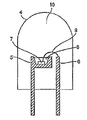
本発明の発光装置を図面に基づいて説明すると、図2は、第1の発光体(350−430nm発光体)と第2の発光体とを有する発光装置の一実施例を示す模式的断面図であり、4は発光装置、5はマウントリード、6はインナーリード、7は第1の発光体(350−430nmの発光体)、8は第2の発光体としての蛍光体含有樹脂部、9は導電性ワイヤー、10はモールド部材である。 The light emitting device of the present invention will be described with reference to the drawings. FIG. 2 is a schematic cross-sectional view showing an embodiment of a light emitting device having a first light emitter (350-430 nm light emitter) and a second light emitter. 4 is a light emitting device, 5 is a mount lead, 6 is an inner lead, 7 is a first light emitter (350-430 nm light emitter), 8 is a phosphor-containing resin portion as a second light emitter, 9 Is a conductive wire, and 10 is a mold member.
本発明の一例である発光装置は、図2に示されるように、一般的な砲弾型の形態をなし、マウントリード5の上部カップ内には、GaN系発光ダイオード等からなる第1の発光体(350−430nm発光体)7が、その上に、蛍光体をシリコン樹脂、エポキシ樹脂やアクリル樹脂等のバインダーに混合、分散させ、カップ内に流し込むことにより第2の発光体として形成された蛍光体含有樹脂部8で被覆されることにより固定されている。一方、第1の発光体7とマウントリード5、及び第1の発光体7とインナーリード6は、それぞれ導電性ワイヤー9で導通されており、これら全体がエポキシ樹脂等によるモールド部材10で被覆、保護されてなる。
As shown in FIG. 2, the light emitting device as an example of the present invention has a general bullet shape, and a first light emitter made of a GaN-based light emitting diode or the like is disposed in the upper cup of the mount lead 5. (350-430 nm illuminant) 7 is a phosphor formed as a second illuminant by mixing and dispersing the phosphor in a binder such as silicon resin, epoxy resin or acrylic resin, and pouring it into the cup. It is fixed by being covered with the body-containing
又、この発光素子1を組み込んだ面発光照明装置11は、図3に示されるように、内面を白色の平滑面等の光不透過性とした方形の保持ケース12の底面に、多数の発光装置13を、その外側に発光装置13の駆動のための電源及び回路等(図示せず。)を設けて配置し、保持ケース12の蓋部に相当する箇所に、乳白色としたアクリル板等の拡散板14を発光の均一化のために固定してなる。
Further, as shown in FIG. 3, the surface emitting
そして、面発光照明装置11を駆動して、発光素子13の第1の発光体に電圧を印加することにより350−430nmの光を発光させ、その発光の一部を、第2の発光体としての蛍光体含有樹脂部における前記蛍光体が吸収し、可視光を発光し、一方、蛍光体に吸収されなかった青色光等との混色により演色性の高い発光が得られ、この光が拡散板14を透過して、図面上方に出射され、保持ケース12の拡散板14面内において均一な明るさの照明光が得られることとなる。
Then, by driving the surface emitting
以下、本発明を実施例によりさらに具体的に説明するが、本発明はその要旨を越えない限り以下の実施例に限定されるものではない。 EXAMPLES Hereinafter, the present invention will be described more specifically with reference to examples. However, the present invention is not limited to the following examples unless it exceeds the gist.
Ba(NO3)2の水溶液、Ca(NO3)2・4H2Oの水溶液、Mg(NO3)2・6H2Oの水溶液、Eu(NO3)3・6H2Oの水溶液、Mn(NO3)2・6H2Oの水溶液、およびコロイダルシリカ(SiO2)の懸濁液(Ba(NO3)2、Ca(NO3)2・4H2O、Mg(NO3)2・6H2O、Eu(NO3)3・6H2O、Mn(NO3)2・6H2O、S
iO2のモル比が1.133:0.378:0.189:0.2:0.1:1)を白金容
器中で混合し、乾燥後、4%の水素を含む窒素ガス流下1050℃で2時間加熱することにより焼成し、蛍光体Ba1.133Ca0.378Mg0.189Eu0.2Mn0.1SiO4(第2の発光体に用いる蛍光体)を製造した。GaN系発光ダイオードの紫外光領域の主波長である4
00nmでこの蛍光体を励起したときの発光スペクトルを測定した。表−1に、その発光ピークの波長、後述の比較例3の発光ピークの強度を100としたときの発光ピークの強度(以下、相対強度、という)、及び半値幅を示す。本蛍光体が、半値幅が十分広く、良好な演色性を与え、かつ、ピーク波長が590−620nm内にある浅い赤色を発光するので、明るく感じられる赤みを発することがわかる。
Ba (NO 3 ) 2 aqueous solution, Ca (NO 3 ) 2 .4H 2 O aqueous solution, Mg (NO 3 ) 2 .6H 2 O aqueous solution, Eu (NO 3 ) 3 .6H 2 O aqueous solution, Mn ( NO 3 ) 2 · 6H 2 O aqueous solution and colloidal silica (SiO 2 ) suspension (Ba (NO 3 ) 2 , Ca (NO 3 ) 2 · 4H 2 O, Mg (NO 3 ) 2 · 6H 2 O, Eu (NO 3 ) 3 · 6H 2 O, Mn (NO 3 ) 2 · 6H 2 O, S
iO 2 molar ratio of 1.133: 0.378: 0.189: 0.2: 0.1: 1) was mixed in a platinum vessel, dried, and then dried at 1050 ° C. under a nitrogen gas flow containing 4% hydrogen. The phosphor Ba 1.133 Ca 0.378 Mg 0.189 Eu 0.2 Mn 0.1 SiO 4 (phosphor used for the second light emitter) was manufactured by heating for 2 hours. 4 which is the dominant wavelength in the ultraviolet region of GaN-based light-emitting diodes
The emission spectrum was measured when the phosphor was excited at 00 nm. Table 1 shows the wavelength of the emission peak, the intensity of the emission peak when the intensity of the emission peak of Comparative Example 3 described later is 100 (hereinafter referred to as relative intensity), and the half-value width. This phosphor has a sufficiently wide half-value width, gives good color rendering properties, and emits a shallow red light having a peak wavelength in the range of 590 to 620 nm.
(比較例1)
Ba(NO3)2の水溶液、Ca(NO3)2・4H2Oの水溶液、Mg(NO3)2・6H2Oの水溶液、Eu(NO3)3・6H2Oの水溶液、およびコロイダルシリカ(SiO2)の懸濁液(Ba(NO3)2、Ca(NO3)2・4H2O、Mg(NO3)2・6H2O、Eu(NO3)3・6H2O、SiO2のモル比が1.2:0.4:0.2:0.2:1)を仕込み原液として使用すること以外は、実施例1と同様にして蛍光体Ba1.2Ca0.4Mg0.2E
u0.2SiO4を製造した。GaN系発光ダイオードの紫外光領域の主波長である400nmでこの蛍光体を励起したときの発光スペクトルを測定した。表−1に、その発光ピークの波長、相対強度、及び半値幅を示す。実施例1の組成においてMnが添加されないと、赤色ピークが現れないことがわかる。
(Comparative Example 1)
Ba (NO 3 ) 2 aqueous solution, Ca (NO 3 ) 2 · 4H 2 O aqueous solution, Mg (NO 3 ) 2 · 6H 2 O aqueous solution, Eu (NO 3 ) 3 · 6H 2 O aqueous solution, and colloidal Silica (SiO 2 ) suspensions (Ba (NO 3 ) 2 , Ca (NO 3 ) 2 .4H 2 O, Mg (NO 3 ) 2 .6H 2 O, Eu (NO 3 ) 3 .6H 2 O, The phosphor Ba 1.2 Ca 0.4 Mg 0.2 E was prepared in the same manner as in Example 1 except that the molar ratio of SiO 2 was 1.2: 0.4: 0.2: 0.2: 1).
u 0.2 SiO 4 was produced. The emission spectrum was measured when this phosphor was excited at 400 nm, which is the dominant wavelength in the ultraviolet region of a GaN-based light emitting diode. Table 1 shows the wavelength, relative intensity, and half-value width of the emission peak. It can be seen that when Mn is not added in the composition of Example 1, no red peak appears.
(比較例2)
Ba(NO3)2の水溶液、Ca(NO3)2・4H2Oの水溶液、Eu(NO3)3・6H2Oの水溶液、およびコロイダルシリカ(SiO2)の懸濁液(Ba(NO3)2、Ca(N
O3)2・4H2O、Eu(NO3)3・6H2O、SiO2のモル比が0.72:1.08:
0.2:1)を仕込み原液として使用すること以外は、実施例1と同様にして蛍光体Ba0.72Ca1.08Eu0.2SiO4を製造した。GaN系発光ダイオードの紫外光領域の主波長である400nmでこの蛍光体を励起したときの発光スペクトルを測定した。表−1に、その発光ピークの波長、相対強度、及び半値幅を示す。Mn成分又はMg成分がない結晶では赤色ピークが現れないことがわかる。
(Comparative Example 2)
Ba (NO 3 ) 2 aqueous solution, Ca (NO 3 ) 2 .4H 2 O aqueous solution, Eu (NO 3 ) 3 .6H 2 O aqueous solution, and colloidal silica (SiO 2 ) suspension (Ba (NO 2 ) 3 ) 2 , Ca (N
The molar ratio of O 3 ) 2 · 4H 2 O, Eu (NO 3 ) 3 · 6H 2 O, SiO 2 is 0.72: 1.08:
The phosphor Ba 0.72 Ca 1.08 Eu 0.2 SiO 4 was produced in the same manner as in Example 1 except that 0.2: 1) was used as the stock solution. The emission spectrum was measured when this phosphor was excited at 400 nm, which is the dominant wavelength in the ultraviolet region of a GaN-based light emitting diode. Table 1 shows the wavelength, relative intensity, and half-value width of the emission peak. It can be seen that a red peak does not appear in crystals having no Mn component or Mg component.
(比較例3)
Ba(NO3)2の水溶液、Eu(NO3)3・6H2Oの水溶液、Mn(NO3)2・6H2Oの水溶液、およびコロイダルシリカ(SiO2)の懸濁液(Ba(NO3)2、Eu(N
O3)3・6H2O、Mn(NO3)2・6H2O、SiO2のモル比が1.6:0.2:0.
2:1)を仕込み原液として使用すること以外は、実施例1と同様にして蛍光体Ba1.6
Eu0.2Mn0.2SiO4を製造した。GaN系発光ダイオードの紫外光領域の主波長であ
る400nmでこの蛍光体を励起したときの発光スペクトルを測定した。表−1に、その発光ピークの波長、相対強度、及び半値幅を示す。結晶中にMnが含まれていても、Ca又はMgがないと、赤色ピークが現れないことがわかる。
(Comparative Example 3)
An aqueous solution of Ba (NO 3 ) 2, an aqueous solution of Eu (NO 3 ) 3 .6H 2 O, an aqueous solution of Mn (NO 3 ) 2 .6H 2 O, and a suspension of colloidal silica (SiO 2 ) (Ba (NO 3 ) 2 , Eu (N
The molar ratio of O 3 ) 3 · 6H 2 O, Mn (NO 3 ) 2 · 6H 2 O, SiO 2 is 1.6: 0.2: 0.
Phosphor Ba 1.6 was obtained in the same manner as in Example 1 except that 2: 1) was used as the stock solution.
Eu 0.2 Mn 0.2 SiO 4 was produced. The emission spectrum was measured when this phosphor was excited at 400 nm, which is the dominant wavelength in the ultraviolet region of a GaN-based light emitting diode. Table 1 shows the wavelength, relative intensity, and half-value width of the emission peak. It can be seen that even if Mn is contained in the crystal, the red peak does not appear without Ca or Mg.
(比較例4)
Ca(NO3)2・4H2Oの水溶液、Eu(NO3)3・6H2Oの水溶液、Mn(NO3
)2・6H2Oの水溶液、およびコロイダルシリカ(SiO2)の懸濁液(Ca(NO3)2
・4H2O、Eu(NO3)3・6H2O、Mn(NO3)2・6H2O、SiO2のモル比が1.6:0.2:0.2:1)を仕込み原液として使用すること以外は、実施例1と同様にして蛍光体Ca1.6Eu0.2Mn0.2SiO4を製造した。GaN系発光ダイオードの紫外光領域の主波長である400nmでこの蛍光体を励起したときの発光スペクトルを測定した。表−1に、その発光ピークの波長、相対強度、及び半値幅を示す。結晶中にMnが含まれていても、Ba又はMgがないと、赤色ピークが現れないことがわかる。
(Comparative Example 4)
An aqueous solution of Ca (NO 3 ) 2 .4H 2 O, an aqueous solution of Eu (NO 3 ) 3 .6H 2 O, Mn (NO 3
) (Suspension of SiO 2) (Ca (NO 3) an aqueous solution of 2 · 6H 2 O and colloidal silica, 2
-4H 2 O, Eu (NO 3 ) 3 · 6H 2 O, Mn (NO 3 ) 2 · 6H 2 O, SiO 2 molar ratio 1.6: 0.2: 0.2: 1) A phosphor Ca 1.6 Eu 0.2 Mn 0.2 SiO 4 was produced in the same manner as in Example 1 except that the above was used. The emission spectrum was measured when this phosphor was excited at 400 nm, which is the dominant wavelength in the ultraviolet region of a GaN-based light emitting diode. Table 1 shows the wavelength, relative intensity, and half-value width of the emission peak. It can be seen that even if Mn is contained in the crystal, the red peak does not appear without Ba or Mg.
(比較例5)
Ba(NO3)2の水溶液、Mg(NO3)2・6H2Oの水溶液、Eu(NO3)3・6H2Oの水溶液、Mn(NO3)2・6H2Oの水溶液、およびコロイダルシリカ(SiO2)の
懸濁液(Ba(NO3)2、Mg(NO3)2・6H2O、Eu(NO3)3・6H2O、Mn(NO3)2・6H2O、SiO2のモル比が0.587:1.173:0.2:0.04:1)を仕込み原液として使用すること以外は、実施例1と同様にして蛍光体Ba0.587Mg1.173Eu0.2Mn0.04SiO4を製造した。GaN系発光ダイオードの紫外光領域の主波長である400nmでこの蛍光体を励起したときの発光スペクトルを測定した。表−1に、その発光ピークの波長、相対強度、及び半値幅を示す。結晶中において、CaがBaに対して適当量存在しないと、ピーク波長が620nmを超えてしまい、明るく感じられる赤みを出すことができないことがわかる。
(Comparative Example 5)
Ba (NO 3 ) 2 aqueous solution, Mg (NO 3 ) 2 · 6H 2 O aqueous solution, Eu (NO 3 ) 3 · 6H 2 O aqueous solution, Mn (NO 3 ) 2 · 6H 2 O aqueous solution, and colloidal Silica (SiO 2 ) suspensions (Ba (NO 3 ) 2 , Mg (NO 3 ) 2 .6H 2 O, Eu (NO 3 ) 3 .6H 2 O, Mn (NO 3 ) 2 .6H 2 O, The phosphor Ba 0.587 Mg 1.173 Eu 0.2 Mn was prepared in the same manner as in Example 1 except that the molar ratio of SiO 2 was 0.587: 1.173: 0.2: 0.04: 1). 0.04 SiO 4 was produced. The emission spectrum was measured when this phosphor was excited at 400 nm, which is the dominant wavelength in the ultraviolet region of a GaN-based light emitting diode. Table 1 shows the wavelength, relative intensity, and half-value width of the emission peak. It can be seen that if the Ca does not exist in an appropriate amount relative to Ba in the crystal, the peak wavelength exceeds 620 nm, and a bright reddishness cannot be produced.
Ba(NO3)2の水溶液、Ca(NO3)2・4H2Oの水溶液、Mg(NO3)2・6H2Oの水溶液、Eu(NO3)3・6H2Oの水溶液、Mn(NO3)2・6H2Oの水溶液、およびコロイダルシリカ(SiO2)の懸濁液(Ba(NO3)2、Ca(NO3)2・4H2O
、Mg(NO3)2・6H2O、Eu(NO3)3・6H2O、Mn(NO3)2・6H2O、S
iO2のモル比が1.173:0.391:0.196:0.2:0.04:1)を仕込
み原液として使用すること以外は、実施例1と同様にして蛍光体Ba1.173Ca0.391Mg0.196Eu0.2Mn0.04SiO4を製造した。GaN系発光ダイオードの紫外光領域の主波
長である400nmでこの蛍光体を励起したときの発光スペクトルを測定した。図4にその発光スペクトルを示す。表−2に、色を表す色度座標のx値,y値、最大ピークの波長、後述の比較例7の蛍光体の最大ピークの強度を100とした場合の、本蛍光体の最大ピークの強度(以下、最大ピークの相対強度、という)、及び、発光スペクトル中、赤成分がどの程度存在するかを知る目安となる最大ピークの強度に対する600nmでの強度の割合、ならびにピーク群の半値幅を示す。青・緑・赤成分がともに十分存在し、スペクトル幅が非常に広く、演色性が高い白色発光となっていることがわかる。
Ba (NO 3 ) 2 aqueous solution, Ca (NO 3 ) 2 .4H 2 O aqueous solution, Mg (NO 3 ) 2 .6H 2 O aqueous solution, Eu (NO 3 ) 3 .6H 2 O aqueous solution, Mn ( NO 3 ) 2 · 6H 2 O aqueous solution and colloidal silica (SiO 2 ) suspension (Ba (NO 3 ) 2 , Ca (NO 3 ) 2 · 4H 2 O
Mg (NO 3 ) 2 · 6H 2 O, Eu (NO 3 ) 3 · 6H 2 O, Mn (NO 3 ) 2 · 6H 2 O, S
The phosphor Ba 1.173 Ca was used in the same manner as in Example 1 except that the molar ratio of iO 2 was 1.173: 0.391: 0.196: 0.2: 0.04: 1). 0.391 Mg 0.196 Eu 0.2 Mn 0.04 SiO 4 was produced. The emission spectrum was measured when this phosphor was excited at 400 nm, which is the dominant wavelength in the ultraviolet region of a GaN-based light emitting diode. FIG. 4 shows the emission spectrum. Table-2 shows the maximum peak of the phosphor when the chromaticity coordinate x value, the y value, the wavelength of the maximum peak, and the intensity of the maximum peak of the phosphor of Comparative Example 7 described later are 100. Intensity (hereinafter referred to as the maximum peak relative intensity), the ratio of the intensity at 600 nm to the intensity of the maximum peak, which serves as a guide to know how much red component is present in the emission spectrum, and the half width of the peak group Indicates. It can be seen that the blue, green and red components are sufficiently present, the spectral width is very wide, and the white light emission has a high color rendering property.
なお、最大ピークとは、発光スペクトル中に複数のピークが存在する場合、最も強度の高いピークのことを指し、単ピークの場合は、それを指す。また、ピーク群の半値幅とは、発光スペクトルがどれだけ幅広く分布していて、どれだけ演色性が高いかを知る目安となるものであり、図5の如く、スペクトル中最大ピークの強度の、半分以上の強度を有する波長領域の幅の総和と定義する。 Note that the maximum peak refers to the peak with the highest intensity when there are a plurality of peaks in the emission spectrum, and refers to that in the case of a single peak. In addition, the half width of the peak group is a guideline for knowing how widely the emission spectrum is distributed and how high the color rendering property is, as shown in FIG. It is defined as the sum of the widths of the wavelength regions having an intensity of more than half.
(比較例6)
Ba(NO3)2の水溶液、Ca(NO3)2・4H2Oの水溶液、Mg(NO3)2・6H2Oの水溶液、Eu(NO3)3・6H2Oの水溶液、およびコロイダルシリカ(SiO2)の懸濁液(Ba(NO3)2、Ca(NO3)2・4H2O、Mg(NO3)2・6H2O、Eu(NO3)3・6H2O、SiO2のモル比が1.2:0.4:0.2:0.2:1)を仕込み原液として使用すること以外は、実施例1と同様にして蛍光体Ba1.2Ca0.4Mg0.2E
u0.2SiO4を製造した。GaN系発光ダイオードの紫外光領域の主波長である400nmでこの蛍光体を励起したときの発光スペクトルを測定した。表−2に、色度座標のx値、y値、最大ピークの波長、最大ピークの相対強度、最大ピークの強度に対する600nmでの強度の割合、ピーク群の半値幅を示す。実施例5の組成においてMnが添加されないと、白色スペクトルとならないことがわかる。
(Comparative Example 6)
Ba (NO 3 ) 2 aqueous solution, Ca (NO 3 ) 2 · 4H 2 O aqueous solution, Mg (NO 3 ) 2 · 6H 2 O aqueous solution, Eu (NO 3 ) 3 · 6H 2 O aqueous solution, and colloidal Silica (SiO 2 ) suspensions (Ba (NO 3 ) 2 , Ca (NO 3 ) 2 .4H 2 O, Mg (NO 3 ) 2 .6H 2 O, Eu (NO 3 ) 3 .6H 2 O, The phosphor Ba 1.2 Ca 0.4 Mg 0.2 E was prepared in the same manner as in Example 1 except that the molar ratio of SiO 2 was 1.2: 0.4: 0.2: 0.2: 1).
u 0.2 SiO 4 was produced. The emission spectrum was measured when this phosphor was excited at 400 nm, which is the dominant wavelength in the ultraviolet region of a GaN-based light emitting diode. Table 2 shows the x value, y value, wavelength of the maximum peak, relative intensity of the maximum peak, the ratio of the intensity at 600 nm to the intensity of the maximum peak, and the half width of the peak group. It can be seen that when Mn is not added in the composition of Example 5, a white spectrum is not obtained.
(比較例7)
Ba(NO3)2の水溶液、Ca(NO3)2・4H2Oの水溶液、Eu(NO3)3・6H2Oの水溶液、およびコロイダルシリカ(SiO2)の懸濁液(Ba(NO3)2、Ca(N
O3)2・4H2O、Eu(NO3)3・6H2O、SiO2のモル比が0.72:1.08:
0.2:1)を仕込み原液として使用すること以外は、実施例1と同様にして蛍光体Ba0.72Ca1.08Eu0.2SiO4を製造した。GaN系発光ダイオードの紫外光領域の主波長である400nmでこの蛍光体を励起したときの発光スペクトルを測定した。表−2に、色度座標のx値、y値、最大ピークの波長、最大ピークの相対強度、最大ピークの強度に対する600nmでの強度の割合、ピーク群の半値幅を示す。結晶中Mn又はMgが存在しないと、白色スペクトルとならないことがわかる。
(Comparative Example 7)
Ba (NO 3 ) 2 aqueous solution, Ca (NO 3 ) 2 .4H 2 O aqueous solution, Eu (NO 3 ) 3 .6H 2 O aqueous solution, and colloidal silica (SiO 2 ) suspension (Ba (NO 2 ) 3 ) 2 , Ca (N
The molar ratio of O 3 ) 2 · 4H 2 O, Eu (NO 3 ) 3 · 6H 2 O, SiO 2 is 0.72: 1.08:
The phosphor Ba 0.72 Ca 1.08 Eu 0.2 SiO 4 was produced in the same manner as in Example 1 except that 0.2: 1) was used as the stock solution. The emission spectrum was measured when this phosphor was excited at 400 nm, which is the dominant wavelength in the ultraviolet region of a GaN-based light emitting diode. Table 2 shows the x value, y value, wavelength of the maximum peak, relative intensity of the maximum peak, the ratio of the intensity at 600 nm to the intensity of the maximum peak, and the half width of the peak group. It can be seen that if there is no Mn or Mg in the crystal, no white spectrum is obtained.
(比較例8)
Ba(NO3)2の水溶液、Mg(NO3)2・6H2Oの水溶液、Eu(NO3)3・6H2Oの水溶液、Mn(NO3)2・6H2Oの水溶液、およびコロイダルシリカ(SiO2)の懸濁液(Ba(NO3)2、Mg(NO3)2・6H2O、Eu(NO3)3・6H2O、Mn(NO3)2・6H2O、SiO2のモル比が0.587:1.173:0.2:0.04:1)を仕込み原液として使用すること以外は、実施例1と同様にして蛍光体Ba0.587Mg1.173Eu0.2Mn0.04SiO4を製造した。GaN系発光ダイオードの紫外光領域の主波長である400nmでこの蛍光体を励起したときの発光スペクトルを測定した。表−2に、色度座標のx値、y値、最大ピークの波長、最大ピークの相対強度、最大ピークの強度に
対する600nmでの強度の割合、ピーク群の半値幅を示す。結晶中において、CaがBaに対して適当量存在しないと、赤色ピークの方の波長が620nmを超えてしまい、明るく感じられる赤みを含まない可視光スペクトルが得られる。
(Comparative Example 8)
Ba (NO 3 ) 2 aqueous solution, Mg (NO 3 ) 2 · 6H 2 O aqueous solution, Eu (NO 3 ) 3 · 6H 2 O aqueous solution, Mn (NO 3 ) 2 · 6H 2 O aqueous solution, and colloidal Silica (SiO 2 ) suspensions (Ba (NO 3 ) 2 , Mg (NO 3 ) 2 .6H 2 O, Eu (NO 3 ) 3 .6H 2 O, Mn (NO 3 ) 2 .6H 2 O, The phosphor Ba 0.587 Mg 1.173 Eu 0.2 Mn was prepared in the same manner as in Example 1 except that the molar ratio of SiO 2 was 0.587: 1.173: 0.2: 0.04: 1). 0.04 SiO 4 was produced. The emission spectrum was measured when this phosphor was excited at 400 nm, which is the dominant wavelength in the ultraviolet region of a GaN-based light emitting diode. Table 2 shows the x value, y value, wavelength of the maximum peak, relative intensity of the maximum peak, the ratio of the intensity at 600 nm to the intensity of the maximum peak, and the half width of the peak group. In the crystal, if an appropriate amount of Ca is not present with respect to Ba, the wavelength of the red peak exceeds 620 nm, and a visible light spectrum that does not contain redness that is felt bright can be obtained.
BaCO3,CaCO3,MgCO3,Eu2O3,MnCO3・nH2O,SiO2のモル比
が1.283:0.428:0.09:0.075:0.05:1となるように計量し、フラックスとしてNH4Clを加えてボールミルで1時間混合した。この調合粉体をアル
ミナ坩堝にいれさらにこの坩堝ごとカーボン坩堝に入れて4%の水素を含む窒素ガス流下1200℃で6時間加熱することにより蛍光体Ba1.283Ca0.428Mg0.09Eu0.15Mn0.05SiO4を製造した。この蛍光体のX線回折測定は以下の条件で行った。走査範囲内
の回折角誤差がΔ2θ=0.05°以下に光学調整されたCuKαのX線源からなるブラッグーブレンターノ型の粉末X線回折装置を用い、かつ試料偏心に伴う回折角の誤差が標準シリコンの111ピークを用いてΔ2θ=0.05°以下の角度再現性が保証される条件で粉末X線回折測定を実施した。また測定時にX線の照射幅が試料の幅を超えないように発散スリットの発散角を調整し、回折ピーク位置(ピークトップ)及び回折強度(高さ)は固定スリットモードでの測定結果の値を読み取った。図6にX線回折測定結果を示す。得られた蛍光体は請求項6に記述した条件を満足していることが表3によって示され、前述した特定の相を含むことが確認された。GaN系発光ダイオードの近紫外領域の主波長である400nmでこの蛍光体を励起したときの発光スペクトルを図7に示した。発光スペクトル上で励起光源の影響を取り除くため、420nm以下の光をカットしている。本蛍光体の色度座標x及びy値、発光ピーク波長、発光ピーク強度を表4に示した。
The molar ratio of BaCO 3 , CaCO 3 , MgCO 3 , Eu 2 O 3 , MnCO 3 .nH 2 O, SiO 2 is 1.283: 0.428: 0.09: 0.075: 0.05: 1. Then, NH 4 Cl was added as a flux and mixed with a ball mill for 1 hour. The prepared powder is put in an alumina crucible, and the whole crucible is put in a carbon crucible and heated at 1200 ° C. for 6 hours under a nitrogen gas flow containing 4% hydrogen to obtain phosphor Ba 1.283 Ca 0.428 Mg 0.09 Eu 0.15 Mn 0.05 SiO 4. Manufactured. X-ray diffraction measurement of this phosphor was performed under the following conditions. Using a Bragg-Brentano type powder X-ray diffractometer consisting of a CuKα X-ray source optically adjusted so that the diffraction angle error within the scanning range is Δ2θ = 0.05 ° or less, and the diffraction angle error due to sample eccentricity is Powder X-ray diffraction measurement was performed under the condition that an angle reproducibility of Δ2θ = 0.05 ° or less was guaranteed using 111 peaks of standard silicon. Also, the divergence angle of the divergence slit is adjusted so that the X-ray irradiation width does not exceed the width of the sample during measurement, and the diffraction peak position (peak top) and diffraction intensity (height) are the values of the measurement results in the fixed slit mode. I read. FIG. 6 shows the X-ray diffraction measurement results. Table 3 shows that the obtained phosphor satisfies the conditions described in claim 6, and it was confirmed that the phosphor contained the specific phase described above. FIG. 7 shows the emission spectrum when this phosphor is excited at 400 nm, which is the dominant wavelength in the near ultraviolet region of the GaN-based light emitting diode. In order to remove the influence of the excitation light source on the emission spectrum, light of 420 nm or less is cut. Table 4 shows the chromaticity coordinates x and y values, emission peak wavelength, and emission peak intensity of this phosphor.
BaCO3,CaCO3,MgCO3,Eu2O3,MnCO3・nH2O,SiO2のモル
比が1.215:0.405:0.180:0.075:0.05:1となるように計量した以外は実施例3と同様にして蛍光体Ba1.215Ca0.405Mg0.18Eu0.15Mn0.05SiO4を得た。表3にX線回折測定結果を示すが本例請求項6の条件を満たしている。図
7に発光スペクトル、表4に特性をまとめた。
The molar ratio of BaCO 3 , CaCO 3 , MgCO 3 , Eu 2 O 3 , MnCO 3 .nH 2 O, SiO 2 is 1.215: 0.405: 0.180: 0.075: 0.05: 1 A phosphor Ba 1.215 Ca 0.405 Mg 0.18 Eu 0.15 Mn 0.05 SiO 4 was obtained in the same manner as in Example 3 except that the amount was measured. Table 3 shows X-ray diffraction measurement results, which satisfy the conditions of claim 6 of this example. FIG. 7 shows the emission spectrum, and Table 4 shows the characteristics.
BaCO3,CaCO3,SrCO3,MgCO3,Eu2O3,MnCO3・nH2O,SiO2のモル比が0.855:0.285:0.57:0.09:0.075:0.05
:1となるように計量した以外は実施例3と同様にして蛍光体Ba0.855Ca0.285Sr0.57Mg0.09Eu0.15Mn0.05SiO4を得た。表3にX線回折測定結果を示すが本例請求
項6の条件を満たしている。図7に発光スペクトル、表4に特性をまとめた。
The molar ratio of BaCO 3 , CaCO 3 , SrCO 3 , MgCO 3 , Eu 2 O 3 , MnCO 3 .nH 2 O, SiO 2 is 0.855: 0.285: 0.57: 0.09: 0.075: 0. 05
The phosphor Ba 0.855 Ca 0.285 Sr 0.57 Mg 0.09 Eu 0.15 Mn 0.05 SiO 4 was obtained in the same manner as in Example 3 except that the weight was adjusted to be 1. Table 3 shows X-ray diffraction measurement results, which satisfy the conditions of claim 6 of this example. FIG. 7 shows the emission spectrum, and Table 4 shows the characteristics.
BaCO3,CaCO3,SrCO3,MgCO3,Eu2O3,MnCO3・nH2O,SiO2のモル比が0.810:0.27:0.54:0.18:0.075:0.05:
1となるように計量した以外は実施例3と同様にして蛍光体Ba0.81Ca0.27Sr0.54Mg0.18Eu0.15Mn0.05SiO4を得た。表3にX線回折測定結果を示すが本例は請求項
6の条件を満たしていない。図7に発光スペクトル、表4に特性をまとめた。
The molar ratio of BaCO 3 , CaCO 3 , SrCO 3 , MgCO 3 , Eu 2 O 3 , MnCO 3 .nH 2 O, SiO 2 is 0.810: 0.27: 0.54: 0.18: 0.075: 0. 05:
A phosphor Ba 0.81 Ca 0.27 Sr 0.54 Mg 0.18 Eu 0.15 Mn 0.05 SiO 4 was obtained in the same manner as in Example 3 except that the weight was adjusted to 1. Table 3 shows the X-ray diffraction measurement results, but this example does not satisfy the conditions of claim 6. FIG. 7 shows the emission spectrum, and Table 4 shows the characteristics.
1 第2の発光体
2 面発光型GaN系LD
3 基板
4 発光装置
5 マウントリード
6 インナーリード
7 第1の発光体(350〜430nmの発光体)
8 本発明中の蛍光体を含有させた樹脂部
9 導電性ワイヤー
10 モールド部材
11 発光素子を組み込んだ面発光照明装置
12 保持ケース
13 発光装置
14 拡散板
DESCRIPTION OF
3 Substrate 4 Light emitting device 5 Mount lead 6
DESCRIPTION OF
Claims (13)
Eu a Mn b Mg c M 1 d M 2 O e ・・・[1]
(但し、M1は、Li,Na,K,Rb及びCsよりなる群から選ばれる1価の元素、Ba,Ca,Sr,V,Cr,Fe,Co,Ni,Cu,Zn,Mo,Ru,Pd,Ag,Cd,Sn,Sm,Tm,Yb,W,Re,Os,Ir,Pt,Hg及びPbよりなる群から選ばれる2価の元素、B,Al,Ga,In,Y及びScよりなる群から選ばれる3価の元素、並びに、P,Sb及びBiよりなる群から選ばれる5価の元素よりなる群から選ばれる少なくとも1種の元素であって、BaとCaとSrの合計が占める割合が80mol%以上であり、BaとCaの合計が占める割合が80mol%以上であり、BaとCaの合計に対するCaの割合(モル比)が0.2以上0.9以下である。M2は、Si,Ge,Zn,Ti及びHfよりなる群から選ばれる少なくとも一種の4価の元素であって、Siが占める割合が80mol%以上である。aは0.001≦a≦0.8、bは0<b≦0.8、c,dは0<c/(c+d)≦0.2、a,b,c,dは1.8≦(a+b+c+d)≦2.2、eは3.6≦e≦4.4を満足する数である。) Have a crystal phase having a chemical composition represented by the following general formula [1], phosphor emission peak at a wavelength of 400nm excitation is characterized by the presence within the 590-620Nm.
Eu a Mn b Mg c M 1 d M 2 O e ... [1]
(However, M 1 is a monovalent element selected from the group consisting of Li, Na, K, Rb and Cs, Ba, Ca, Sr, V, Cr, Fe, Co, Ni, Cu, Zn, Mo, Ru. , Pd, Ag, Cd, Sn, Sm, Tm, Yb, W, Re, Os, Ir, Pt, Hg and Pb, a divalent element selected from the group consisting of B, Al, Ga, In, Y and Sc A trivalent element selected from the group consisting of: and at least one element selected from the group consisting of pentavalent elements selected from the group consisting of P, Sb and Bi, and the sum of Ba , Ca and Sr The proportion of Ba and Ca is 80 mol% or more, and the ratio of Ca to the total of Ba and Ca (molar ratio) is 0.2 or more and 0.9 or less. .M 2 is, Si, Ge, Zn, Ti and and at least one tetravalent element selected from the group consisting of f, .a percentage Si is is not less than 80 mol% is 0.001 ≦ a ≦ 0.8, b is 0 <b ≦ 0.8 , C, d satisfy 0 <c / (c + d) ≦ 0.2, a, b, c, d satisfy 1.8 ≦ (a + b + c + d) ≦ 2.2, e satisfy 3.6 ≦ e ≦ 4.4 Number to do.)
Priority Applications (1)
| Application Number | Priority Date | Filing Date | Title |
|---|---|---|---|
| JP2005007207A JP4617889B2 (en) | 2004-01-16 | 2005-01-14 | Phosphor, and light emitting device, lighting device, and image display device using the same |
Applications Claiming Priority (2)
| Application Number | Priority Date | Filing Date | Title |
|---|---|---|---|
| JP2004009769 | 2004-01-16 | ||
| JP2005007207A JP4617889B2 (en) | 2004-01-16 | 2005-01-14 | Phosphor, and light emitting device, lighting device, and image display device using the same |
Publications (3)
| Publication Number | Publication Date |
|---|---|
| JP2005226068A JP2005226068A (en) | 2005-08-25 |
| JP2005226068A5 JP2005226068A5 (en) | 2007-06-21 |
| JP4617889B2 true JP4617889B2 (en) | 2011-01-26 |
Family
ID=35001028
Family Applications (1)
| Application Number | Title | Priority Date | Filing Date |
|---|---|---|---|
| JP2005007207A Expired - Fee Related JP4617889B2 (en) | 2004-01-16 | 2005-01-14 | Phosphor, and light emitting device, lighting device, and image display device using the same |
Country Status (1)
| Country | Link |
|---|---|
| JP (1) | JP4617889B2 (en) |
Families Citing this family (3)
| Publication number | Priority date | Publication date | Assignee | Title |
|---|---|---|---|---|
| US7489073B2 (en) * | 2005-04-15 | 2009-02-10 | Patent-Treuhand-Gesellschaft für elektrische Glühlampen mbH | Blue to yellow-orange emitting phosphor, and light source having such a phosphor |
| EP1995294A4 (en) * | 2006-02-10 | 2012-06-06 | Mitsubishi Chem Corp | Phosphor, method for producing same, phosphor-containing composition, light-emitting device, image display, and illuminating device |
| JP2008095091A (en) * | 2006-09-15 | 2008-04-24 | Mitsubishi Chemicals Corp | Fluorescent substance and its production method, fluorescent substance containing composition, light emitting device, image display device, and illuminating device |
Citations (5)
| Publication number | Priority date | Publication date | Assignee | Title |
|---|---|---|---|---|
| JPH09194833A (en) * | 1996-01-22 | 1997-07-29 | Kasei Optonix Co Ltd | Photostimulable phosphor |
| JP2000282032A (en) * | 1999-03-30 | 2000-10-10 | Taiheiyo Keizai Kaihatsu:Kk | Luminous fluophor composition |
| WO2002011214A1 (en) * | 2000-07-28 | 2002-02-07 | Patent Treuhand Gesellschaft für elektrische Glühlampen mbH | Illumination device with at least one led as the light source |
| JP2003306675A (en) * | 2002-02-15 | 2003-10-31 | Mitsubishi Chemicals Corp | Light-emitting device and illumination device using the same |
| WO2004056940A1 (en) * | 2002-12-20 | 2004-07-08 | Toyoda Gosei Co., Ltd. | Phosphor and optical device using same |
-
2005
- 2005-01-14 JP JP2005007207A patent/JP4617889B2/en not_active Expired - Fee Related
Patent Citations (5)
| Publication number | Priority date | Publication date | Assignee | Title |
|---|---|---|---|---|
| JPH09194833A (en) * | 1996-01-22 | 1997-07-29 | Kasei Optonix Co Ltd | Photostimulable phosphor |
| JP2000282032A (en) * | 1999-03-30 | 2000-10-10 | Taiheiyo Keizai Kaihatsu:Kk | Luminous fluophor composition |
| WO2002011214A1 (en) * | 2000-07-28 | 2002-02-07 | Patent Treuhand Gesellschaft für elektrische Glühlampen mbH | Illumination device with at least one led as the light source |
| JP2003306675A (en) * | 2002-02-15 | 2003-10-31 | Mitsubishi Chemicals Corp | Light-emitting device and illumination device using the same |
| WO2004056940A1 (en) * | 2002-12-20 | 2004-07-08 | Toyoda Gosei Co., Ltd. | Phosphor and optical device using same |
Also Published As
| Publication number | Publication date |
|---|---|
| JP2005226068A (en) | 2005-08-25 |
Similar Documents
| Publication | Publication Date | Title |
|---|---|---|
| US7608200B2 (en) | Phosphor and including the same, light emitting apparatus, illuminating apparatus and image display | |
| JP4617890B2 (en) | Phosphor, and light emitting device, lighting device, and image display device using the same | |
| JP2005298805A (en) | Light emitting device and illumination device | |
| JP4168776B2 (en) | LIGHT EMITTING DEVICE AND LIGHTING DEVICE USING THE SAME | |
| JP4706358B2 (en) | Blue light emitting phosphor and method for manufacturing the same, light emitting device, illumination device, backlight for display and display | |
| JP4617889B2 (en) | Phosphor, and light emitting device, lighting device, and image display device using the same | |
| JP4617888B2 (en) | Phosphor, and light emitting device, lighting device, and image display device using the same | |
| JP4972904B2 (en) | Phosphor, method for manufacturing the phosphor, light-emitting device using the phosphor, image display device, and illumination device | |
| JP4165255B2 (en) | LIGHT EMITTING DEVICE AND LIGHTING DEVICE USING THE SAME | |
| JP2007009141A (en) | Blue light-emitting phosphor and its manufacturing method, light-emitting apparatus, illumination apparatus, back light for display, and display | |
| JP4411841B2 (en) | LIGHT EMITTING DEVICE, LIGHTING DEVICE USING SAME, AND DISPLAY | |
| JP4389513B2 (en) | Light emitting device, lighting device, and image display device | |
| JP4561064B2 (en) | Light emitting device, lighting device, and image display device | |
| JP4363194B2 (en) | Phosphor, and light emitting device, lighting device, and image display device using the same | |
| JP5326986B2 (en) | Phosphor used in light emitting device | |
| JP2004235546A (en) | Light emitting device and lighting device and display using it | |
| JP4337468B2 (en) | Light emitting device, lighting device, and image display device | |
| JP2005064189A (en) | Light emitting device, lighting device and image display device | |
| JP2010059429A (en) | Phosphor, luminescent device using the same, image display and illuminating device | |
| JP4337465B2 (en) | Light emitting device, lighting device, and image display device | |
| JP4604516B2 (en) | LIGHT EMITTING DEVICE, LIGHTING DEVICE USING SAME, AND DISPLAY | |
| JP4246502B2 (en) | LIGHT EMITTING DEVICE, LIGHTING DEVICE USING SAME, AND DISPLAY | |
| JP4433847B2 (en) | Phosphor, light emitting device using the same, image display device, and illumination device | |
| JP4380118B2 (en) | LIGHT EMITTING DEVICE AND LIGHTING DEVICE USING THE SAME | |
| JP4513287B2 (en) | Light emitting device, lighting device, and image display device |
Legal Events
| Date | Code | Title | Description |
|---|---|---|---|
| A521 | Written amendment |
Free format text: JAPANESE INTERMEDIATE CODE: A523 Effective date: 20070508 |
|
| A621 | Written request for application examination |
Free format text: JAPANESE INTERMEDIATE CODE: A621 Effective date: 20070508 |
|
| RD05 | Notification of revocation of power of attorney |
Free format text: JAPANESE INTERMEDIATE CODE: A7425 Effective date: 20090619 |
|
| A131 | Notification of reasons for refusal |
Free format text: JAPANESE INTERMEDIATE CODE: A131 Effective date: 20100525 |
|
| A521 | Written amendment |
Free format text: JAPANESE INTERMEDIATE CODE: A523 Effective date: 20100723 |
|
| TRDD | Decision of grant or rejection written | ||
| A01 | Written decision to grant a patent or to grant a registration (utility model) |
Free format text: JAPANESE INTERMEDIATE CODE: A01 Effective date: 20100928 |
|
| A01 | Written decision to grant a patent or to grant a registration (utility model) |
Free format text: JAPANESE INTERMEDIATE CODE: A01 |
|
| A61 | First payment of annual fees (during grant procedure) |
Free format text: JAPANESE INTERMEDIATE CODE: A61 Effective date: 20101011 |
|
| FPAY | Renewal fee payment (event date is renewal date of database) |
Free format text: PAYMENT UNTIL: 20131105 Year of fee payment: 3 |
|
| R150 | Certificate of patent or registration of utility model |
Free format text: JAPANESE INTERMEDIATE CODE: R150 |
|
| LAPS | Cancellation because of no payment of annual fees |