JPWO2012164792A1 - 発光装置、面光源、液晶ディスプレイ装置、およびレンズ - Google Patents
発光装置、面光源、液晶ディスプレイ装置、およびレンズ Download PDFInfo
- Publication number
- JPWO2012164792A1 JPWO2012164792A1 JP2012553129A JP2012553129A JPWO2012164792A1 JP WO2012164792 A1 JPWO2012164792 A1 JP WO2012164792A1 JP 2012553129 A JP2012553129 A JP 2012553129A JP 2012553129 A JP2012553129 A JP 2012553129A JP WO2012164792 A1 JPWO2012164792 A1 JP WO2012164792A1
- Authority
- JP
- Japan
- Prior art keywords
- light
- light emitting
- lens
- optical axis
- light source
- Prior art date
- Legal status (The legal status is an assumption and is not a legal conclusion. Google has not performed a legal analysis and makes no representation as to the accuracy of the status listed.)
- Granted
Links
Images


Classifications
-
- F—MECHANICAL ENGINEERING; LIGHTING; HEATING; WEAPONS; BLASTING
- F21—LIGHTING
- F21V—FUNCTIONAL FEATURES OR DETAILS OF LIGHTING DEVICES OR SYSTEMS THEREOF; STRUCTURAL COMBINATIONS OF LIGHTING DEVICES WITH OTHER ARTICLES, NOT OTHERWISE PROVIDED FOR
- F21V5/00—Refractors for light sources
- F21V5/04—Refractors for light sources of lens shape
-
- G—PHYSICS
- G02—OPTICS
- G02B—OPTICAL ELEMENTS, SYSTEMS OR APPARATUS
- G02B19/00—Condensers, e.g. light collectors or similar non-imaging optics
- G02B19/0004—Condensers, e.g. light collectors or similar non-imaging optics characterised by the optical means employed
- G02B19/0009—Condensers, e.g. light collectors or similar non-imaging optics characterised by the optical means employed having refractive surfaces only
- G02B19/0014—Condensers, e.g. light collectors or similar non-imaging optics characterised by the optical means employed having refractive surfaces only at least one surface having optical power
-
- G—PHYSICS
- G02—OPTICS
- G02B—OPTICAL ELEMENTS, SYSTEMS OR APPARATUS
- G02B19/00—Condensers, e.g. light collectors or similar non-imaging optics
- G02B19/0033—Condensers, e.g. light collectors or similar non-imaging optics characterised by the use
- G02B19/0047—Condensers, e.g. light collectors or similar non-imaging optics characterised by the use for use with a light source
-
- G—PHYSICS
- G02—OPTICS
- G02F—OPTICAL DEVICES OR ARRANGEMENTS FOR THE CONTROL OF LIGHT BY MODIFICATION OF THE OPTICAL PROPERTIES OF THE MEDIA OF THE ELEMENTS INVOLVED THEREIN; NON-LINEAR OPTICS; FREQUENCY-CHANGING OF LIGHT; OPTICAL LOGIC ELEMENTS; OPTICAL ANALOGUE/DIGITAL CONVERTERS
- G02F1/00—Devices or arrangements for the control of the intensity, colour, phase, polarisation or direction of light arriving from an independent light source, e.g. switching, gating or modulating; Non-linear optics
- G02F1/01—Devices or arrangements for the control of the intensity, colour, phase, polarisation or direction of light arriving from an independent light source, e.g. switching, gating or modulating; Non-linear optics for the control of the intensity, phase, polarisation or colour
- G02F1/13—Devices or arrangements for the control of the intensity, colour, phase, polarisation or direction of light arriving from an independent light source, e.g. switching, gating or modulating; Non-linear optics for the control of the intensity, phase, polarisation or colour based on liquid crystals, e.g. single liquid crystal display cells
- G02F1/133—Constructional arrangements; Operation of liquid crystal cells; Circuit arrangements
- G02F1/1333—Constructional arrangements; Manufacturing methods
- G02F1/1335—Structural association of cells with optical devices, e.g. polarisers or reflectors
- G02F1/1336—Illuminating devices
- G02F1/133602—Direct backlight
- G02F1/133603—Direct backlight with LEDs
-
- G—PHYSICS
- G02—OPTICS
- G02F—OPTICAL DEVICES OR ARRANGEMENTS FOR THE CONTROL OF LIGHT BY MODIFICATION OF THE OPTICAL PROPERTIES OF THE MEDIA OF THE ELEMENTS INVOLVED THEREIN; NON-LINEAR OPTICS; FREQUENCY-CHANGING OF LIGHT; OPTICAL LOGIC ELEMENTS; OPTICAL ANALOGUE/DIGITAL CONVERTERS
- G02F1/00—Devices or arrangements for the control of the intensity, colour, phase, polarisation or direction of light arriving from an independent light source, e.g. switching, gating or modulating; Non-linear optics
- G02F1/01—Devices or arrangements for the control of the intensity, colour, phase, polarisation or direction of light arriving from an independent light source, e.g. switching, gating or modulating; Non-linear optics for the control of the intensity, phase, polarisation or colour
- G02F1/13—Devices or arrangements for the control of the intensity, colour, phase, polarisation or direction of light arriving from an independent light source, e.g. switching, gating or modulating; Non-linear optics for the control of the intensity, phase, polarisation or colour based on liquid crystals, e.g. single liquid crystal display cells
- G02F1/133—Constructional arrangements; Operation of liquid crystal cells; Circuit arrangements
- G02F1/1333—Constructional arrangements; Manufacturing methods
- G02F1/1335—Structural association of cells with optical devices, e.g. polarisers or reflectors
- G02F1/1336—Illuminating devices
- G02F1/133602—Direct backlight
- G02F1/133606—Direct backlight including a specially adapted diffusing, scattering or light controlling members
-
- F—MECHANICAL ENGINEERING; LIGHTING; HEATING; WEAPONS; BLASTING
- F21—LIGHTING
- F21V—FUNCTIONAL FEATURES OR DETAILS OF LIGHTING DEVICES OR SYSTEMS THEREOF; STRUCTURAL COMBINATIONS OF LIGHTING DEVICES WITH OTHER ARTICLES, NOT OTHERWISE PROVIDED FOR
- F21V13/00—Producing particular characteristics or distribution of the light emitted by means of a combination of elements specified in two or more of main groups F21V1/00 - F21V11/00
- F21V13/02—Combinations of only two kinds of elements
- F21V13/04—Combinations of only two kinds of elements the elements being reflectors and refractors
-
- F—MECHANICAL ENGINEERING; LIGHTING; HEATING; WEAPONS; BLASTING
- F21—LIGHTING
- F21V—FUNCTIONAL FEATURES OR DETAILS OF LIGHTING DEVICES OR SYSTEMS THEREOF; STRUCTURAL COMBINATIONS OF LIGHTING DEVICES WITH OTHER ARTICLES, NOT OTHERWISE PROVIDED FOR
- F21V7/00—Reflectors for light sources
- F21V7/0091—Reflectors for light sources using total internal reflection
-
- F—MECHANICAL ENGINEERING; LIGHTING; HEATING; WEAPONS; BLASTING
- F21—LIGHTING
- F21Y—INDEXING SCHEME ASSOCIATED WITH SUBCLASSES F21K, F21L, F21S and F21V, RELATING TO THE FORM OR THE KIND OF THE LIGHT SOURCES OR OF THE COLOUR OF THE LIGHT EMITTED
- F21Y2105/00—Planar light sources
- F21Y2105/10—Planar light sources comprising a two-dimensional array of point-like light-generating elements
-
- F—MECHANICAL ENGINEERING; LIGHTING; HEATING; WEAPONS; BLASTING
- F21—LIGHTING
- F21Y—INDEXING SCHEME ASSOCIATED WITH SUBCLASSES F21K, F21L, F21S and F21V, RELATING TO THE FORM OR THE KIND OF THE LIGHT SOURCES OR OF THE COLOUR OF THE LIGHT EMITTED
- F21Y2115/00—Light-generating elements of semiconductor light sources
- F21Y2115/10—Light-emitting diodes [LED]
-
- G—PHYSICS
- G02—OPTICS
- G02F—OPTICAL DEVICES OR ARRANGEMENTS FOR THE CONTROL OF LIGHT BY MODIFICATION OF THE OPTICAL PROPERTIES OF THE MEDIA OF THE ELEMENTS INVOLVED THEREIN; NON-LINEAR OPTICS; FREQUENCY-CHANGING OF LIGHT; OPTICAL LOGIC ELEMENTS; OPTICAL ANALOGUE/DIGITAL CONVERTERS
- G02F1/00—Devices or arrangements for the control of the intensity, colour, phase, polarisation or direction of light arriving from an independent light source, e.g. switching, gating or modulating; Non-linear optics
- G02F1/01—Devices or arrangements for the control of the intensity, colour, phase, polarisation or direction of light arriving from an independent light source, e.g. switching, gating or modulating; Non-linear optics for the control of the intensity, phase, polarisation or colour
- G02F1/13—Devices or arrangements for the control of the intensity, colour, phase, polarisation or direction of light arriving from an independent light source, e.g. switching, gating or modulating; Non-linear optics for the control of the intensity, phase, polarisation or colour based on liquid crystals, e.g. single liquid crystal display cells
- G02F1/133—Constructional arrangements; Operation of liquid crystal cells; Circuit arrangements
- G02F1/1333—Constructional arrangements; Manufacturing methods
- G02F1/1335—Structural association of cells with optical devices, e.g. polarisers or reflectors
- G02F1/1336—Illuminating devices
- G02F1/133602—Direct backlight
- G02F1/133606—Direct backlight including a specially adapted diffusing, scattering or light controlling members
- G02F1/133607—Direct backlight including a specially adapted diffusing, scattering or light controlling members the light controlling member including light directing or refracting elements, e.g. prisms or lenses
-
- G—PHYSICS
- G02—OPTICS
- G02F—OPTICAL DEVICES OR ARRANGEMENTS FOR THE CONTROL OF LIGHT BY MODIFICATION OF THE OPTICAL PROPERTIES OF THE MEDIA OF THE ELEMENTS INVOLVED THEREIN; NON-LINEAR OPTICS; FREQUENCY-CHANGING OF LIGHT; OPTICAL LOGIC ELEMENTS; OPTICAL ANALOGUE/DIGITAL CONVERTERS
- G02F1/00—Devices or arrangements for the control of the intensity, colour, phase, polarisation or direction of light arriving from an independent light source, e.g. switching, gating or modulating; Non-linear optics
- G02F1/01—Devices or arrangements for the control of the intensity, colour, phase, polarisation or direction of light arriving from an independent light source, e.g. switching, gating or modulating; Non-linear optics for the control of the intensity, phase, polarisation or colour
- G02F1/13—Devices or arrangements for the control of the intensity, colour, phase, polarisation or direction of light arriving from an independent light source, e.g. switching, gating or modulating; Non-linear optics for the control of the intensity, phase, polarisation or colour based on liquid crystals, e.g. single liquid crystal display cells
- G02F1/133—Constructional arrangements; Operation of liquid crystal cells; Circuit arrangements
- G02F1/1333—Constructional arrangements; Manufacturing methods
- G02F1/1335—Structural association of cells with optical devices, e.g. polarisers or reflectors
- G02F1/1336—Illuminating devices
- G02F1/133602—Direct backlight
- G02F1/133611—Direct backlight including means for improving the brightness uniformity
-
- H—ELECTRICITY
- H01—ELECTRIC ELEMENTS
- H01L—SEMICONDUCTOR DEVICES NOT COVERED BY CLASS H10
- H01L25/00—Assemblies consisting of a plurality of individual semiconductor or other solid state devices ; Multistep manufacturing processes thereof
- H01L25/03—Assemblies consisting of a plurality of individual semiconductor or other solid state devices ; Multistep manufacturing processes thereof all the devices being of a type provided for in the same subgroup of groups H01L27/00 - H01L33/00, or in a single subclass of H10K, H10N, e.g. assemblies of rectifier diodes
- H01L25/04—Assemblies consisting of a plurality of individual semiconductor or other solid state devices ; Multistep manufacturing processes thereof all the devices being of a type provided for in the same subgroup of groups H01L27/00 - H01L33/00, or in a single subclass of H10K, H10N, e.g. assemblies of rectifier diodes the devices not having separate containers
- H01L25/075—Assemblies consisting of a plurality of individual semiconductor or other solid state devices ; Multistep manufacturing processes thereof all the devices being of a type provided for in the same subgroup of groups H01L27/00 - H01L33/00, or in a single subclass of H10K, H10N, e.g. assemblies of rectifier diodes the devices not having separate containers the devices being of a type provided for in group H01L33/00
- H01L25/0753—Assemblies consisting of a plurality of individual semiconductor or other solid state devices ; Multistep manufacturing processes thereof all the devices being of a type provided for in the same subgroup of groups H01L27/00 - H01L33/00, or in a single subclass of H10K, H10N, e.g. assemblies of rectifier diodes the devices not having separate containers the devices being of a type provided for in group H01L33/00 the devices being arranged next to each other
-
- H—ELECTRICITY
- H01—ELECTRIC ELEMENTS
- H01L—SEMICONDUCTOR DEVICES NOT COVERED BY CLASS H10
- H01L2924/00—Indexing scheme for arrangements or methods for connecting or disconnecting semiconductor or solid-state bodies as covered by H01L24/00
- H01L2924/0001—Technical content checked by a classifier
- H01L2924/0002—Not covered by any one of groups H01L24/00, H01L24/00 and H01L2224/00
-
- H—ELECTRICITY
- H01—ELECTRIC ELEMENTS
- H01L—SEMICONDUCTOR DEVICES NOT COVERED BY CLASS H10
- H01L33/00—Semiconductor devices with at least one potential-jump barrier or surface barrier specially adapted for light emission; Processes or apparatus specially adapted for the manufacture or treatment thereof or of parts thereof; Details thereof
- H01L33/48—Semiconductor devices with at least one potential-jump barrier or surface barrier specially adapted for light emission; Processes or apparatus specially adapted for the manufacture or treatment thereof or of parts thereof; Details thereof characterised by the semiconductor body packages
- H01L33/58—Optical field-shaping elements
Abstract
Description
即ち、本発明の第1態様における発光装置は、光軸を中心として光を放射する発光装置であって、発光素子、および前記発光素子を覆い蛍光体を分散させた樹脂を有する光源と、前記光源からの光を放射状に拡張するレンズとを備え、前記レンズは、前記光軸と直交する第1方向と、前記光軸および前記第1方向に直交する第2方向との屈折力が異なる。
図1は、本発明の実施の形態1に係る液晶ディスプレイ装置101の全体の概略構成を示す図である。この液晶ディスプレイ装置101は、液晶表示パネル8と、液晶表示パネル8の裏側(反表示面側)に配置された面光源7とを備えている。面光源7は、発光装置1と、発光装置1に対向して設置される拡散板4とを有する。尚、面光源7については、以下の実施の形態2にて詳しく説明する。
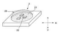
ここでは、本発明の実施の形態2に係る面光源7について、詳しく説明する。図2は、面光源7の構成図である。この面光源7は、上述したように、複数の発光装置1と、これらの発光装置1を覆うように配置される拡散板4とを備えている。発光装置1は、光源2と光源2を覆って配置されるレンズ3とを有する。拡散板4は、光源2の光軸に対して直交方向に延在する。また、発光装置1は、筐体内の底部に配置され、底部に対向する筐体の開口部を拡散板4で閉止して、面光源7が形成される。なお、発光装置1は、拡散板4の全面又は略全面に対向して平面的に分散して配置されていればよく、図2に示すように、マトリクス状に配置されていてもよいし、千鳥状に配置されていてもよく、その配置形態を問わない。
発光装置1を構成する光源2およびレンズ3については、以下の実施の形態3にて詳しく説明する。
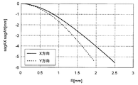
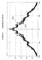
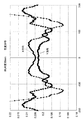
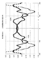
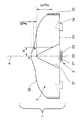
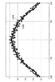
ここでは、本発明の実施の形態3に係る発光装置1について、詳しく説明する。図4ならびに図5Aおよび5Bに、発光装置1の構成を示す。この発光装置1は、既に説明したように、光源2と、光源2からの光を放射状に拡張するレンズ3とを備え、例えば拡散板4の被照射面4aに、光軸Aを中心として略円形状に光を放射するものである。すなわち、光源2からの光の方向性がレンズ3で広げられ、これにより拡散板4の被照射面4aにおける光軸Aを中心とする広い範囲が照明される。被照射面4aの照度分布は、光軸A上が最大で、周囲に行くほど略単調に減少する。
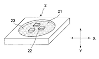
実施例1において、光源2は、発光面21の大きさが、おおよそφ3.0mmの汎用品のLEDを採用し、光源2からの光の方向性を広げ、色ムラを抑えることを目的としている。実施例1において、レンズ3の有効径は、20.7mmとなっている。また、光軸中心でのレンズの厚みが1.2mmとなっている。実施例1の具体的な数値を表1に示す。

本発明は、添付図面を参照しながら好ましい実施形態に関連して充分に記載されているが、この技術の熟練した人々にとっては種々の変形や修正は明白である。そのような変形や修正は、添付した請求の範囲による本発明の範囲から外れない限りにおいて、その中に含まれると理解されるべきである。
又、2011年5月31日に出願された、日本国特許出願No.特願2011−121373号の明細書、図面、特許請求の範囲、及び要約書の開示内容の全ては、参考として本明細書中に編入されるものである。
2 光源
3 レンズ
4 拡散板
5 基板
6 反射シート ないし 反射コーティング膜
7 面光源
8 液晶表示パネル
21 発光面
22 発光素子
23 蛍光体を分散させた透明樹脂
31 入射面
32 出射面
33 底面
34 反射部
35 リング部
即ち、本発明の第1態様における発光装置は、光軸を中心として光を放射する発光装置であって、発光素子、および前記発光素子を覆い蛍光体を分散させた樹脂を有する光源と、前記光源からの光を放射状に拡張するレンズとを備え、前記レンズは、前記光軸と直交する第1方向と、前記光軸および前記第1方向に直交する第2方向との屈折力が異なる。
図1は、本発明の実施の形態1に係る液晶ディスプレイ装置101の全体の概略構成を示す図である。この液晶ディスプレイ装置101は、液晶表示パネル8と、液晶表示パネル8の裏側(反表示面側)に配置された面光源7とを備えている。面光源7は、発光装置1と、発光装置1に対向して設置される拡散板4とを有する。尚、面光源7については、以下の実施の形態2にて詳しく説明する。
ここでは、本発明の実施の形態2に係る面光源7について、詳しく説明する。図2は、面光源7の構成図である。この面光源7は、上述したように、複数の発光装置1と、これらの発光装置1を覆うように配置される拡散板4とを備えている。発光装置1は、光源2と光源2を覆って配置されるレンズ3とを有する。拡散板4は、光源2の光軸に対して直交方向に延在する。また、発光装置1は、筐体内の底部に配置され、底部に対向する筐体の開口部を拡散板4で閉止して、面光源7が形成される。なお、発光装置1は、拡散板4の全面又は略全面に対向して平面的に分散して配置されていればよく、図2に示すように、マトリクス状に配置されていてもよいし、千鳥状に配置されていてもよく、その配置形態を問わない。
発光装置1を構成する光源2およびレンズ3については、以下の実施の形態3にて詳しく説明する。
ここでは、本発明の実施の形態3に係る発光装置1について、詳しく説明する。図4ならびに図5Aおよび5Bに、発光装置1の構成を示す。この発光装置1は、既に説明したように、光源2と、光源2からの光を放射状に拡張するレンズ3とを備え、例えば拡散板4の被照射面4aに、光軸Aを中心として略円形状に光を放射するものである。すなわち、光源2からの光の方向性がレンズ3で広げられ、これにより拡散板4の被照射面4aにおける光軸Aを中心とする広い範囲が照明される。被照射面4aの照度分布は、光軸A上が最大で、周囲に行くほど略単調に減少する。
実施例1において、光源2は、発光面21の大きさが、おおよそφ3.0mmの汎用品のLEDを採用し、光源2からの光の方向性を広げ、色ムラを抑えることを目的としている。実施例1において、レンズ3の有効径は、20.7mmとなっている。また、光軸中心でのレンズの厚みが1.2mmとなっている。実施例1の具体的な数値を表1に示す。
本発明は、添付図面を参照しながら好ましい実施形態に関連して充分に記載されているが、この技術の熟練した人々にとっては種々の変形や修正は明白である。そのような変形や修正は、添付した請求の範囲による本発明の範囲から外れない限りにおいて、その中に含まれると理解されるべきである。
又、2011年5月31日に出願された、日本国特許出願No.特願2011−121373号の明細書、図面、特許請求の範囲、及び要約書の開示内容の全ては、参考として本明細書中に編入されるものである。
2 光源
3 レンズ
4 拡散板
5 基板
6 反射シート ないし 反射コーティング膜
7 面光源
8 液晶表示パネル
21 発光面
22 発光素子
23 蛍光体を分散させた透明樹脂
31 入射面
32 出射面
33 底面
34 反射部
35 リング部
Claims (18)
- 光源(2)およびこの光源を覆って配置され光源からの光を拡張するレンズ(3)を有する発光装置(1)において、
前記レンズは、光軸を中心として光源からの光が入射する入射面(31)と、入射した光を放射状に拡張して出射する出射面(32)と、を有し、
前記入射面は、連続する凹面を有し、前記出射面は、連続する凸面を有し、かつ前記レンズは、前記光軸に直交する第1方向と、前記光軸および前記第1方向に直交する第2方向との屈折力が異なる、
発光装置。 - 前記入射面が、第1方向および第2方向で屈折力を異ならせた、アナモフィックな非球面の曲面を含む、請求項1に記載の発光装置。
- 前記レンズは、前記入射面の周囲に位置し前記出射面と反対側に位置する底面(33)をさらに有し、
前記底面には、光軸に沿って凹形状の反射部(34)を有する、請求項1に記載の発光装置。 - 前記入射面は、第1方向および第2方向で屈折力を異ならせた、アナモフィックな非球面の曲面を含む凹面であり、
前記出射面は、前記光軸に対して回転対称な凸面である、請求項3に記載の発光装置。 - 前記反射部は、光軸を中心とした円状又は楕円状に配置されている、請求項3に記載の発光装置。
- 前記反射部は、前記底面とのなす角θが、次の条件式、
15°<θ<45°
を満足する、請求項3に記載の発光装置。 - 前記反射部は、前記レンズの有効半径の65%以上、光軸から外側の位置に少なくとも1つ配置されている、請求項3に記載の発光装置。
- 前記光源は、発光素子(22)と、該発光素子上にドーム状に形成された蛍光体層(23)とを含み、前記蛍光体層の表面に発光面(21)が構成されている、請求項1に記載の発光装置。
- 光源(2)およびこの光源を覆って配置され光源からの光を拡張するレンズ(3)を有する複数個の発光装置(1)と、
前記発光装置に対向して配置され光源の光軸に直交して延在する拡散板(4)と、
前記発光装置から出射した光を前記拡散板側に反射させる反射用部材(6)と、
を備え、
前記レンズは、光源の光軸に直交する第1方向と、前記光軸および前記第1方向に直交する第2方向との屈折力が異なり、
複数個の前記発光装置は、前記拡散板に対向して分散して配置される、
面光源。 - 液晶表示パネル(8)と、該液晶表示パネルの背面側に配置され、該液晶表示パネルに対応する大きさの面光源(7)とを備えた液晶ディスプレイ装置であって、前記面光源は、複数個の光源(2)および該光源を覆って配置され光源からの光を拡張するレンズ(3)を有する発光装置(1)と、発光装置に対向して前記液晶表示パネルに隣接して配置され光源の光軸に直交して延在する拡散板(4)と、前記発光装置から出射した光を前記拡散板側に反射させる反射用部材(6)と、を備えた液晶ディスプレイ装置(101)において、
前記面光源は、複数個の前記発光装置を、前記拡散板に対向して分散させて配置し、
前記発光装置のレンズは、光軸を中心として光源からの光が入射する入射面(31)と、入射した光を放射状に拡張して出射する出射面(32)と、を有し、
前記入射面は、連続する凹面を有し、前記出射面は、連続する凸面を有し、かつ前記レンズは、前記入射面および前記出射面の少なくとも一方において、前記光軸に直交する第1方向と、前記光軸および前記第1方向に直交する第2方向との屈折力が異なる、
液晶ディスプレイ装置。 - 発光ダイオード(2)からの光を拡張するレンズ(3)において、
前記レンズは、光軸を中心として発光ダイオードからの光が入射する入射面(31)と、入射した光を放射状に拡張して出射する出射面(32)と、を有し、
前記入射面は、連続する凹面を有し、前記出射面は、連続する凸面を有し、かつ前記レンズは、前記入射面および前記出射面の少なくとも一方において、前記光軸に直交する第1方向と、前記光軸および前記第1方向に直交する第2方向との屈折力が異なる、
レンズ。 - 前記入射面は、第1方向および第2方向で屈折力を異ならせた、アナモフィックな非球面の曲面を含む、請求項11に記載のレンズ。
- 前記入射面の周囲に位置し前記出射面と反対側に位置する底面(33)をさらに有し、
前記底面には、光軸に沿って凹形状の反射部(34)を有する、請求項11に記載のレンズ。 - 前記入射面は、第1方向および第2方向で屈折力を異ならせた、アナモフィックな非球面の曲面を含む凹面であり、
前記出射面は、前記光軸に対して回転対称な凸面である、請求項13に記載のレンズ。 - 前記反射部は、光軸を中心とした円状又は楕円状に配置されている、請求項13に記載のレンズ。
- 前記反射部は、前記底面とのなす角θが、次の条件式
15°<θ<45°
を満足する、請求項13に記載のレンズ。 - 前記反射部は、前記レンズの有効半径の65%以上、光軸から外側の位置に少なくとも1つ配置されている、請求項13に記載のレンズ。
- 前記発光ダイオードは、発光素子(22)と、該発光素子上にドーム状に形成された蛍光体層(23)とを含み、前記蛍光体層の表面に発光面(21)が構成されている、請求項11に記載のレンズ。
Priority Applications (1)
| Application Number | Priority Date | Filing Date | Title |
|---|---|---|---|
| JP2012553129A JP5849193B2 (ja) | 2011-05-31 | 2012-02-29 | 発光装置、面光源、液晶ディスプレイ装置、およびレンズ |
Applications Claiming Priority (4)
| Application Number | Priority Date | Filing Date | Title |
|---|---|---|---|
| JP2011121373 | 2011-05-31 | ||
| JP2011121373 | 2011-05-31 | ||
| PCT/JP2012/001369 WO2012164792A1 (ja) | 2011-05-31 | 2012-02-29 | 発光装置、面光源、液晶ディスプレイ装置、およびレンズ |
| JP2012553129A JP5849193B2 (ja) | 2011-05-31 | 2012-02-29 | 発光装置、面光源、液晶ディスプレイ装置、およびレンズ |
Publications (2)
| Publication Number | Publication Date |
|---|---|
| JPWO2012164792A1 true JPWO2012164792A1 (ja) | 2014-07-31 |
| JP5849193B2 JP5849193B2 (ja) | 2016-01-27 |
Family
ID=47258670
Family Applications (1)
| Application Number | Title | Priority Date | Filing Date |
|---|---|---|---|
| JP2012553129A Expired - Fee Related JP5849193B2 (ja) | 2011-05-31 | 2012-02-29 | 発光装置、面光源、液晶ディスプレイ装置、およびレンズ |
Country Status (3)
| Country | Link |
|---|---|
| US (1) | US20130114022A1 (ja) |
| JP (1) | JP5849193B2 (ja) |
| WO (1) | WO2012164792A1 (ja) |
Families Citing this family (18)
| Publication number | Priority date | Publication date | Assignee | Title |
|---|---|---|---|---|
| WO2012164791A1 (ja) * | 2011-05-31 | 2012-12-06 | パナソニック株式会社 | 面光源および液晶ディスプレイ装置 |
| WO2013072429A1 (en) * | 2011-11-17 | 2013-05-23 | Osram Gmbh | Led illuminating device |
| US10047930B2 (en) * | 2011-12-02 | 2018-08-14 | Seoul Semiconductor Co., Ltd. | Light emitting module and lens |
| US9080739B1 (en) * | 2012-09-14 | 2015-07-14 | Cooper Technologies Company | System for producing a slender illumination pattern from a light emitting diode |
| CN103471009A (zh) * | 2013-09-13 | 2013-12-25 | 东莞市欧科光电科技有限公司 | 新型led透镜和液晶显示背光屏 |
| KR102450726B1 (ko) * | 2015-04-29 | 2022-10-05 | 쑤저우 레킨 세미컨덕터 컴퍼니 리미티드 | 광학 렌즈, 발광 모듈 및 이를 구비한 라이트 유닛 |
| KR102538400B1 (ko) * | 2015-12-18 | 2023-06-01 | 쑤저우 레킨 세미컨덕터 컴퍼니 리미티드 | 광학 렌즈, 발광 모듈 및 이를 구비한 라이트 유닛 |
| US10393341B2 (en) | 2015-04-24 | 2019-08-27 | Abl Ip Holding Llc | Tri-lobe optic and associated light fixtures |
| USD779112S1 (en) | 2015-04-24 | 2017-02-14 | Abl Ip Holding Llc | Tri-lobe light fixture optic |
| KR102374202B1 (ko) * | 2015-05-26 | 2022-03-14 | 쑤저우 레킨 세미컨덕터 컴퍼니 리미티드 | 광학 렌즈, 조명 모듈 및 이를 구비한 라이트 유닛 |
| KR101666844B1 (ko) * | 2015-09-10 | 2016-10-19 | 삼성전자주식회사 | 광학 소자 및 이를 포함하는 광원 모듈 |
| US9640741B1 (en) * | 2015-11-01 | 2017-05-02 | Artled Technology Corp. | Concentrating lens of a light emitting diode lamp |
| US9985182B2 (en) * | 2015-12-25 | 2018-05-29 | Citizen Electronics Co., Ltd. | Light-emitting apparatus and color-matching apparatus |
| EP3208533B1 (en) * | 2016-02-16 | 2018-11-21 | LG Innotek Co., Ltd. | Optical lens and light emitting module including the same |
| CN106992241A (zh) * | 2017-04-01 | 2017-07-28 | 惠州市华瑞光源科技有限公司 | Led灯条及led面光源模组 |
| KR102077388B1 (ko) * | 2018-03-12 | 2020-02-13 | (주)엔디에스 | 엘이디 확산렌즈 |
| CN113958883A (zh) | 2018-03-15 | 2022-01-21 | 首尔半导体株式会社 | 发光模块及透镜 |
| KR20190109221A (ko) | 2018-03-15 | 2019-09-25 | 서울반도체 주식회사 | 디스플레이 장치, 백라이트 유닛, 발광모듈 및 렌즈 |
Family Cites Families (9)
| Publication number | Priority date | Publication date | Assignee | Title |
|---|---|---|---|---|
| JP3115370U (ja) * | 2005-08-02 | 2005-11-04 | 岡谷電機産業株式会社 | 表示ランプ |
| JP5342939B2 (ja) * | 2009-06-19 | 2013-11-13 | パナソニック株式会社 | 照明用レンズ、発光装置、面光源および液晶ディスプレイ装置 |
| JP2011009052A (ja) * | 2009-06-25 | 2011-01-13 | Panasonic Corp | 面光源および液晶ディスプレイ装置 |
| JP5380182B2 (ja) * | 2009-07-03 | 2014-01-08 | パナソニック株式会社 | 発光装置、面光源および液晶ディスプレイ装置 |
| WO2011004642A1 (ja) * | 2009-07-06 | 2011-01-13 | シャープ株式会社 | レンズ、発光素子パッケージ、発光モジュール、照明装置、表示装置、およびテレビ受像装置 |
| JP2011023204A (ja) * | 2009-07-15 | 2011-02-03 | Sharp Corp | 発光装置、光束制御部材および当該発光装置を備える照明装置 |
| JP2011040664A (ja) * | 2009-08-18 | 2011-02-24 | Panasonic Corp | 面光源および液晶ディスプレイ装置 |
| JP5081988B2 (ja) * | 2009-10-19 | 2012-11-28 | パナソニック株式会社 | 照明用レンズ、発光装置、面光源および液晶ディスプレイ装置 |
| WO2012164791A1 (ja) * | 2011-05-31 | 2012-12-06 | パナソニック株式会社 | 面光源および液晶ディスプレイ装置 |
-
2012
- 2012-02-29 WO PCT/JP2012/001369 patent/WO2012164792A1/ja active Application Filing
- 2012-02-29 JP JP2012553129A patent/JP5849193B2/ja not_active Expired - Fee Related
- 2012-12-27 US US13/728,585 patent/US20130114022A1/en not_active Abandoned
Also Published As
| Publication number | Publication date |
|---|---|
| WO2012164792A1 (ja) | 2012-12-06 |
| JP5849193B2 (ja) | 2016-01-27 |
| US20130114022A1 (en) | 2013-05-09 |
Similar Documents
| Publication | Publication Date | Title |
|---|---|---|
| JP5849193B2 (ja) | 発光装置、面光源、液晶ディスプレイ装置、およびレンズ | |
| JP5518881B2 (ja) | 発光装置、面光源および液晶ディスプレイ装置 | |
| JP5325639B2 (ja) | 発光装置 | |
| JP5416662B2 (ja) | 照明用レンズ、発光装置、面光源および液晶ディスプレイ装置 | |
| WO2012164790A1 (ja) | 面光源および液晶ディスプレイ装置 | |
| JP5081988B2 (ja) | 照明用レンズ、発光装置、面光源および液晶ディスプレイ装置 | |
| JP4870950B2 (ja) | 光放射用光源ユニット及びそれを用いた面状発光装置 | |
| US8324796B2 (en) | Lighting device with phosphor layer and lens, and surface light source, and liquid-crystal display | |
| JP5342939B2 (ja) | 照明用レンズ、発光装置、面光源および液晶ディスプレイ装置 | |
| JP2011014831A (ja) | 発光装置、面光源および液晶ディスプレイ装置 | |
| JP5118617B2 (ja) | 照明用レンズ、発光装置、面光源および液晶ディスプレイ装置 | |
| JP2011009052A (ja) | 面光源および液晶ディスプレイ装置 | |
| JP5849192B2 (ja) | 面光源および液晶ディスプレイ装置 | |
| JP2010186142A (ja) | 照明用レンズ、発光装置、面光源および液晶ディスプレイ装置 | |
| JP5342938B2 (ja) | 照明用レンズ、発光装置、面光源および液晶ディスプレイ装置 | |
| JP2010146986A (ja) | 照明用レンズ、発光装置、面光源および液晶ディスプレイ装置 | |
| JP2011228226A (ja) | 照明用レンズ、発光装置、面光源および液晶ディスプレイ装置 | |
| JP5342940B2 (ja) | 照明用レンズ、発光装置、面光源および液晶ディスプレイ装置 | |
| JP2011198479A (ja) | 面光源および液晶ディスプレイ装置 | |
| JP5342941B2 (ja) | 照明用レンズ、発光装置、面光源および液晶ディスプレイ装置 | |
| JP2010146987A (ja) | 照明用レンズ、発光装置、面光源および液晶ディスプレイ装置 |
Legal Events
| Date | Code | Title | Description |
|---|---|---|---|
| A711 | Notification of change in applicant |
Free format text: JAPANESE INTERMEDIATE CODE: A711 Effective date: 20141008 |
|
| RD03 | Notification of appointment of power of attorney |
Free format text: JAPANESE INTERMEDIATE CODE: A7423 Effective date: 20141014 |
|
| A131 | Notification of reasons for refusal |
Free format text: JAPANESE INTERMEDIATE CODE: A131 Effective date: 20141104 |
|
| A521 | Request for written amendment filed |
Free format text: JAPANESE INTERMEDIATE CODE: A523 Effective date: 20141226 |
|
| A131 | Notification of reasons for refusal |
Free format text: JAPANESE INTERMEDIATE CODE: A131 Effective date: 20150203 |
|
| TRDD | Decision of grant or rejection written | ||
| A01 | Written decision to grant a patent or to grant a registration (utility model) |
Free format text: JAPANESE INTERMEDIATE CODE: A01 Effective date: 20150623 |
|
| A61 | First payment of annual fees (during grant procedure) |
Free format text: JAPANESE INTERMEDIATE CODE: A61 Effective date: 20150706 |
|
| R151 | Written notification of patent or utility model registration |
Ref document number: 5849193 Country of ref document: JP Free format text: JAPANESE INTERMEDIATE CODE: R151 |
|
| LAPS | Cancellation because of no payment of annual fees |