JPWO2012164792A1 - Light emitting device, surface light source, liquid crystal display device, and lens - Google Patents
Light emitting device, surface light source, liquid crystal display device, and lens Download PDFInfo
- Publication number
- JPWO2012164792A1 JPWO2012164792A1 JP2012553129A JP2012553129A JPWO2012164792A1 JP WO2012164792 A1 JPWO2012164792 A1 JP WO2012164792A1 JP 2012553129 A JP2012553129 A JP 2012553129A JP 2012553129 A JP2012553129 A JP 2012553129A JP WO2012164792 A1 JPWO2012164792 A1 JP WO2012164792A1
- Authority
- JP
- Japan
- Prior art keywords
- light
- light emitting
- lens
- optical axis
- light source
- Prior art date
- Legal status (The legal status is an assumption and is not a legal conclusion. Google has not performed a legal analysis and makes no representation as to the accuracy of the status listed.)
- Granted
Links
Images


Classifications
-
- F—MECHANICAL ENGINEERING; LIGHTING; HEATING; WEAPONS; BLASTING
- F21—LIGHTING
- F21V—FUNCTIONAL FEATURES OR DETAILS OF LIGHTING DEVICES OR SYSTEMS THEREOF; STRUCTURAL COMBINATIONS OF LIGHTING DEVICES WITH OTHER ARTICLES, NOT OTHERWISE PROVIDED FOR
- F21V5/00—Refractors for light sources
- F21V5/04—Refractors for light sources of lens shape
-
- G—PHYSICS
- G02—OPTICS
- G02B—OPTICAL ELEMENTS, SYSTEMS OR APPARATUS
- G02B19/00—Condensers, e.g. light collectors or similar non-imaging optics
- G02B19/0004—Condensers, e.g. light collectors or similar non-imaging optics characterised by the optical means employed
- G02B19/0009—Condensers, e.g. light collectors or similar non-imaging optics characterised by the optical means employed having refractive surfaces only
- G02B19/0014—Condensers, e.g. light collectors or similar non-imaging optics characterised by the optical means employed having refractive surfaces only at least one surface having optical power
-
- G—PHYSICS
- G02—OPTICS
- G02B—OPTICAL ELEMENTS, SYSTEMS OR APPARATUS
- G02B19/00—Condensers, e.g. light collectors or similar non-imaging optics
- G02B19/0033—Condensers, e.g. light collectors or similar non-imaging optics characterised by the use
- G02B19/0047—Condensers, e.g. light collectors or similar non-imaging optics characterised by the use for use with a light source
-
- G—PHYSICS
- G02—OPTICS
- G02F—OPTICAL DEVICES OR ARRANGEMENTS FOR THE CONTROL OF LIGHT BY MODIFICATION OF THE OPTICAL PROPERTIES OF THE MEDIA OF THE ELEMENTS INVOLVED THEREIN; NON-LINEAR OPTICS; FREQUENCY-CHANGING OF LIGHT; OPTICAL LOGIC ELEMENTS; OPTICAL ANALOGUE/DIGITAL CONVERTERS
- G02F1/00—Devices or arrangements for the control of the intensity, colour, phase, polarisation or direction of light arriving from an independent light source, e.g. switching, gating or modulating; Non-linear optics
- G02F1/01—Devices or arrangements for the control of the intensity, colour, phase, polarisation or direction of light arriving from an independent light source, e.g. switching, gating or modulating; Non-linear optics for the control of the intensity, phase, polarisation or colour
- G02F1/13—Devices or arrangements for the control of the intensity, colour, phase, polarisation or direction of light arriving from an independent light source, e.g. switching, gating or modulating; Non-linear optics for the control of the intensity, phase, polarisation or colour based on liquid crystals, e.g. single liquid crystal display cells
- G02F1/133—Constructional arrangements; Operation of liquid crystal cells; Circuit arrangements
- G02F1/1333—Constructional arrangements; Manufacturing methods
- G02F1/1335—Structural association of cells with optical devices, e.g. polarisers or reflectors
- G02F1/1336—Illuminating devices
- G02F1/133602—Direct backlight
- G02F1/133603—Direct backlight with LEDs
-
- G—PHYSICS
- G02—OPTICS
- G02F—OPTICAL DEVICES OR ARRANGEMENTS FOR THE CONTROL OF LIGHT BY MODIFICATION OF THE OPTICAL PROPERTIES OF THE MEDIA OF THE ELEMENTS INVOLVED THEREIN; NON-LINEAR OPTICS; FREQUENCY-CHANGING OF LIGHT; OPTICAL LOGIC ELEMENTS; OPTICAL ANALOGUE/DIGITAL CONVERTERS
- G02F1/00—Devices or arrangements for the control of the intensity, colour, phase, polarisation or direction of light arriving from an independent light source, e.g. switching, gating or modulating; Non-linear optics
- G02F1/01—Devices or arrangements for the control of the intensity, colour, phase, polarisation or direction of light arriving from an independent light source, e.g. switching, gating or modulating; Non-linear optics for the control of the intensity, phase, polarisation or colour
- G02F1/13—Devices or arrangements for the control of the intensity, colour, phase, polarisation or direction of light arriving from an independent light source, e.g. switching, gating or modulating; Non-linear optics for the control of the intensity, phase, polarisation or colour based on liquid crystals, e.g. single liquid crystal display cells
- G02F1/133—Constructional arrangements; Operation of liquid crystal cells; Circuit arrangements
- G02F1/1333—Constructional arrangements; Manufacturing methods
- G02F1/1335—Structural association of cells with optical devices, e.g. polarisers or reflectors
- G02F1/1336—Illuminating devices
- G02F1/133602—Direct backlight
- G02F1/133606—Direct backlight including a specially adapted diffusing, scattering or light controlling members
-
- F—MECHANICAL ENGINEERING; LIGHTING; HEATING; WEAPONS; BLASTING
- F21—LIGHTING
- F21V—FUNCTIONAL FEATURES OR DETAILS OF LIGHTING DEVICES OR SYSTEMS THEREOF; STRUCTURAL COMBINATIONS OF LIGHTING DEVICES WITH OTHER ARTICLES, NOT OTHERWISE PROVIDED FOR
- F21V13/00—Producing particular characteristics or distribution of the light emitted by means of a combination of elements specified in two or more of main groups F21V1/00 - F21V11/00
- F21V13/02—Combinations of only two kinds of elements
- F21V13/04—Combinations of only two kinds of elements the elements being reflectors and refractors
-
- F—MECHANICAL ENGINEERING; LIGHTING; HEATING; WEAPONS; BLASTING
- F21—LIGHTING
- F21V—FUNCTIONAL FEATURES OR DETAILS OF LIGHTING DEVICES OR SYSTEMS THEREOF; STRUCTURAL COMBINATIONS OF LIGHTING DEVICES WITH OTHER ARTICLES, NOT OTHERWISE PROVIDED FOR
- F21V7/00—Reflectors for light sources
- F21V7/0091—Reflectors for light sources using total internal reflection
-
- F—MECHANICAL ENGINEERING; LIGHTING; HEATING; WEAPONS; BLASTING
- F21—LIGHTING
- F21Y—INDEXING SCHEME ASSOCIATED WITH SUBCLASSES F21K, F21L, F21S and F21V, RELATING TO THE FORM OR THE KIND OF THE LIGHT SOURCES OR OF THE COLOUR OF THE LIGHT EMITTED
- F21Y2105/00—Planar light sources
- F21Y2105/10—Planar light sources comprising a two-dimensional array of point-like light-generating elements
-
- F—MECHANICAL ENGINEERING; LIGHTING; HEATING; WEAPONS; BLASTING
- F21—LIGHTING
- F21Y—INDEXING SCHEME ASSOCIATED WITH SUBCLASSES F21K, F21L, F21S and F21V, RELATING TO THE FORM OR THE KIND OF THE LIGHT SOURCES OR OF THE COLOUR OF THE LIGHT EMITTED
- F21Y2115/00—Light-generating elements of semiconductor light sources
- F21Y2115/10—Light-emitting diodes [LED]
-
- G—PHYSICS
- G02—OPTICS
- G02F—OPTICAL DEVICES OR ARRANGEMENTS FOR THE CONTROL OF LIGHT BY MODIFICATION OF THE OPTICAL PROPERTIES OF THE MEDIA OF THE ELEMENTS INVOLVED THEREIN; NON-LINEAR OPTICS; FREQUENCY-CHANGING OF LIGHT; OPTICAL LOGIC ELEMENTS; OPTICAL ANALOGUE/DIGITAL CONVERTERS
- G02F1/00—Devices or arrangements for the control of the intensity, colour, phase, polarisation or direction of light arriving from an independent light source, e.g. switching, gating or modulating; Non-linear optics
- G02F1/01—Devices or arrangements for the control of the intensity, colour, phase, polarisation or direction of light arriving from an independent light source, e.g. switching, gating or modulating; Non-linear optics for the control of the intensity, phase, polarisation or colour
- G02F1/13—Devices or arrangements for the control of the intensity, colour, phase, polarisation or direction of light arriving from an independent light source, e.g. switching, gating or modulating; Non-linear optics for the control of the intensity, phase, polarisation or colour based on liquid crystals, e.g. single liquid crystal display cells
- G02F1/133—Constructional arrangements; Operation of liquid crystal cells; Circuit arrangements
- G02F1/1333—Constructional arrangements; Manufacturing methods
- G02F1/1335—Structural association of cells with optical devices, e.g. polarisers or reflectors
- G02F1/1336—Illuminating devices
- G02F1/133602—Direct backlight
- G02F1/133606—Direct backlight including a specially adapted diffusing, scattering or light controlling members
- G02F1/133607—Direct backlight including a specially adapted diffusing, scattering or light controlling members the light controlling member including light directing or refracting elements, e.g. prisms or lenses
-
- G—PHYSICS
- G02—OPTICS
- G02F—OPTICAL DEVICES OR ARRANGEMENTS FOR THE CONTROL OF LIGHT BY MODIFICATION OF THE OPTICAL PROPERTIES OF THE MEDIA OF THE ELEMENTS INVOLVED THEREIN; NON-LINEAR OPTICS; FREQUENCY-CHANGING OF LIGHT; OPTICAL LOGIC ELEMENTS; OPTICAL ANALOGUE/DIGITAL CONVERTERS
- G02F1/00—Devices or arrangements for the control of the intensity, colour, phase, polarisation or direction of light arriving from an independent light source, e.g. switching, gating or modulating; Non-linear optics
- G02F1/01—Devices or arrangements for the control of the intensity, colour, phase, polarisation or direction of light arriving from an independent light source, e.g. switching, gating or modulating; Non-linear optics for the control of the intensity, phase, polarisation or colour
- G02F1/13—Devices or arrangements for the control of the intensity, colour, phase, polarisation or direction of light arriving from an independent light source, e.g. switching, gating or modulating; Non-linear optics for the control of the intensity, phase, polarisation or colour based on liquid crystals, e.g. single liquid crystal display cells
- G02F1/133—Constructional arrangements; Operation of liquid crystal cells; Circuit arrangements
- G02F1/1333—Constructional arrangements; Manufacturing methods
- G02F1/1335—Structural association of cells with optical devices, e.g. polarisers or reflectors
- G02F1/1336—Illuminating devices
- G02F1/133602—Direct backlight
- G02F1/133611—Direct backlight including means for improving the brightness uniformity
-
- H—ELECTRICITY
- H01—ELECTRIC ELEMENTS
- H01L—SEMICONDUCTOR DEVICES NOT COVERED BY CLASS H10
- H01L25/00—Assemblies consisting of a plurality of individual semiconductor or other solid state devices ; Multistep manufacturing processes thereof
- H01L25/03—Assemblies consisting of a plurality of individual semiconductor or other solid state devices ; Multistep manufacturing processes thereof all the devices being of a type provided for in the same subgroup of groups H01L27/00 - H01L33/00, or in a single subclass of H10K, H10N, e.g. assemblies of rectifier diodes
- H01L25/04—Assemblies consisting of a plurality of individual semiconductor or other solid state devices ; Multistep manufacturing processes thereof all the devices being of a type provided for in the same subgroup of groups H01L27/00 - H01L33/00, or in a single subclass of H10K, H10N, e.g. assemblies of rectifier diodes the devices not having separate containers
- H01L25/075—Assemblies consisting of a plurality of individual semiconductor or other solid state devices ; Multistep manufacturing processes thereof all the devices being of a type provided for in the same subgroup of groups H01L27/00 - H01L33/00, or in a single subclass of H10K, H10N, e.g. assemblies of rectifier diodes the devices not having separate containers the devices being of a type provided for in group H01L33/00
- H01L25/0753—Assemblies consisting of a plurality of individual semiconductor or other solid state devices ; Multistep manufacturing processes thereof all the devices being of a type provided for in the same subgroup of groups H01L27/00 - H01L33/00, or in a single subclass of H10K, H10N, e.g. assemblies of rectifier diodes the devices not having separate containers the devices being of a type provided for in group H01L33/00 the devices being arranged next to each other
-
- H—ELECTRICITY
- H01—ELECTRIC ELEMENTS
- H01L—SEMICONDUCTOR DEVICES NOT COVERED BY CLASS H10
- H01L2924/00—Indexing scheme for arrangements or methods for connecting or disconnecting semiconductor or solid-state bodies as covered by H01L24/00
- H01L2924/0001—Technical content checked by a classifier
- H01L2924/0002—Not covered by any one of groups H01L24/00, H01L24/00 and H01L2224/00
-
- H—ELECTRICITY
- H01—ELECTRIC ELEMENTS
- H01L—SEMICONDUCTOR DEVICES NOT COVERED BY CLASS H10
- H01L33/00—Semiconductor devices with at least one potential-jump barrier or surface barrier specially adapted for light emission; Processes or apparatus specially adapted for the manufacture or treatment thereof or of parts thereof; Details thereof
- H01L33/48—Semiconductor devices with at least one potential-jump barrier or surface barrier specially adapted for light emission; Processes or apparatus specially adapted for the manufacture or treatment thereof or of parts thereof; Details thereof characterised by the semiconductor body packages
- H01L33/58—Optical field-shaping elements
Abstract
光を広げるパワーの強いレンズを用いながら、輝度及び色が共に均一化された、低コストで省エネルギーの発光装置、この発光装置を有する面光源、この面光源を有する液晶ディスプレイ装置、および発光装置に備わるレンズを提供する。発光装置(1)は、複数個の発光ダイオード(2)およびこの発光ダイオードからの光を拡張するレンズ(3)を有する。レンズは、光軸を中心として発光ダイオードからの光が入射する入射面(31)と、入射した光を放射状に拡張して出射する出射面(32)とを有する。入射面は、連続する凹面を有し、出射面は、連続する凸面を有し、かつレンズは、光軸に直交する第1方向と、光軸および第1方向に直交する第2方向との屈折力が異なる。A low-cost and energy-saving light-emitting device in which both brightness and color are made uniform while using a powerful lens that spreads light, a surface light source having the light-emitting device, a liquid crystal display device having the surface light source, and a light-emitting device Provide provided lenses. The light emitting device (1) has a plurality of light emitting diodes (2) and a lens (3) for expanding light from the light emitting diodes. The lens has an incident surface (31) on which light from the light emitting diode is incident with the optical axis as the center, and an exit surface (32) that radially expands and emits the incident light. The incident surface has a continuous concave surface, the output surface has a continuous convex surface, and the lens has a first direction orthogonal to the optical axis and a second direction orthogonal to the optical axis and the first direction. The refractive power is different.
Description
本発明は、例えば発光ダイオード(以下単に「LED」という。)等の光源からの光の方向性をレンズで広げる発光装置に関する。また、本発明は、この発光装置を複数備える面光源、およびこの面光源がバックライトとして液晶表示パネル後方に配置された液晶ディスプレイ装置、さらに、発光装置に備わるレンズに関する。 The present invention relates to a light emitting device that spreads the directionality of light from a light source such as a light emitting diode (hereinafter simply referred to as “LED”) with a lens. The present invention also relates to a surface light source including a plurality of the light emitting devices, a liquid crystal display device in which the surface light sources are arranged behind the liquid crystal display panel as a backlight, and a lens provided in the light emitting device.
従来の大型の液晶ディスプレイ装置のバックライトでは、冷陰極管が液晶表示パネル直下に多数配置され、これらの冷陰極管が拡散板や反射板等の部材と共に使われていた。近年では、バックライトの光源としてLEDが使用されるようになっている。LEDは、近年、発光効率が向上し、蛍光灯に変わる消費電力の少ない光源として期待されている。また液晶ディスプレイ装置用の光源としては映像に応じてLEDの明暗を制御することで液晶ディスプレイ装置の消費電力を下げることができる。 In the backlight of a conventional large-sized liquid crystal display device, a large number of cold cathode tubes are arranged directly under the liquid crystal display panel, and these cold cathode tubes are used together with members such as a diffusion plate and a reflector. In recent years, LEDs have been used as light sources for backlights. In recent years, LEDs have been expected as light sources with improved luminous efficiency and low power consumption, replacing fluorescent lamps. Further, as a light source for a liquid crystal display device, the power consumption of the liquid crystal display device can be reduced by controlling the brightness of the LED according to the image.
液晶ディスプレイ装置において、LEDを光源とするバックライトでは、冷陰極管の代わりに多数のLEDを配置することとなる。多数のLEDを用いることでバックライト表面に均一な明るさを得ることができるが、多数のLEDが必要なことから、安価にできない問題があった。この欠点を解決すべく、1個のLEDの出力を大きくし、使用するLEDの個数を減らす取り組みがなされている。例えば特許文献1では、少ない個数のLEDでも均一な輝度の面光源が得られるようにする発光装置が提案されている。
In a liquid crystal display device, in a backlight using LEDs as light sources, a large number of LEDs are arranged instead of cold cathode tubes. By using a large number of LEDs, a uniform brightness can be obtained on the surface of the backlight. However, since a large number of LEDs are required, there is a problem that the cost cannot be reduced. In order to solve this drawback, efforts have been made to increase the output of one LED and reduce the number of LEDs used. For example,
少ない個数のLEDで均一な輝度の面光源を得るためには、1個のLEDで照明可能な照明領域を大きくする必要がある。このために特許文献1の発光装置では、LEDからの光をレンズで放射状に拡張している。これにより、LEDからの光の方向性が広げられ、被照射面において、LEDの光軸を中心とする広い範囲を照明することができる。具体的に、特許文献1の発光装置に用いられるレンズは、平面視で円形状をなしており、光入射面と光制御出射面とが共に光軸に対して回転対称な形状である。ここで、光入射面は、凹面にて形成され、光制御出射面は、光軸近傍部分が凹面で光軸近傍部分の外側部分が凸面にて形成されている。
In order to obtain a surface light source having a uniform luminance with a small number of LEDs, it is necessary to enlarge an illumination area that can be illuminated with one LED. For this reason, in the light emitting device of
一方、特許文献2には、光出射面の中央に、光軸と直交する方向に延びるV溝が形成されたレンズを用いた発光装置が開示されている。この発光装置のレンズによれば、LEDからの光は、V溝が延びる方向(縦方向)には、正規分布の角度分布を保ったまま拡張されるが、V溝が延びる方向と直交する方向(横方向)には、角度分布が光軸近傍では大きく窪み、その両側では急峻に立ち上がるように拡張される。
On the other hand,
近年の白色LEDは、青色LED素子に、YAG系やTAG系などの蛍光体を設けて、疑似白色光を生成するものが主流となっている。このような光源は、パッケージに青色LED素子をボンディングし、青色LED素子を覆うように蛍光体を分散させた透明樹脂を充填して作られている。 In recent years, white LEDs are mainly produced by providing pseudo-white light by providing phosphors such as YAG and TAG in a blue LED element. Such a light source is made by bonding a blue LED element to a package and filling a transparent resin in which a phosphor is dispersed so as to cover the blue LED element.
このような光源は、青色LED素子による青色の光と、青色の光により励起された蛍光体が発光して作る黄色の光とで擬似白色の光を得ているため、青色の発光面サイズと、黄色の発光面のサイズとが異なる。そのため、このようなLEDの光を、特許文献1にあるようなレンズを用いて広げた場合、色によって光の広がりに差が生じ、光源からの光が照射される面光源内の被照射面において色ムラが生じてしまうことになる。またこの色ムラは、光を広げるパワーが強いレンズほど顕著になる傾向にある。
Such a light source obtains pseudo-white light from blue light produced by a blue LED element and yellow light produced by a phosphor excited by blue light, and therefore has a blue light emitting surface size. The size of the yellow light emitting surface is different. Therefore, when such LED light is spread using a lens as in
LEDの発光効率が向上しつつある近年においては、光源1つあたりの、上記被照射面における照射面積を広げ、なおかつ、輝度及び色が共に均一化された、低コストで省エネルギーの発光装置が望まれる。 In recent years when the luminous efficiency of LEDs is improving, a low-cost and energy-saving light-emitting device is desired in which the irradiation area per surface of the light source is increased on the surface to be irradiated and the luminance and color are both uniform. It is.
なお、特許文献2の発光装置は、放射する光に意図的に異方性を作り出すものであるため、上述の要望を満たすものではない。
In addition, since the light-emitting device of
本発明は、上述の要望に鑑み、光を広げる力がある広配光レンズを用いながら、光源が持っている異なる色の光によって生じる被照射面の色ムラを軽減することができ、輝度及び色が共に均一化された発光装置を提供するとともに、この発光装置を含む面光源、および液晶ディスプレイ装置、さらに発光装置に備わるレンズを提供することを目的とする。 In view of the above-described demand, the present invention can reduce unevenness in color of an irradiated surface caused by light of different colors possessed by a light source while using a wide light distribution lens that has the ability to spread light. It is an object of the present invention to provide a light-emitting device in which both colors are uniform, and to provide a surface light source including the light-emitting device, a liquid crystal display device, and a lens included in the light-emitting device.
上記目的を達成するため、本発明は以下のように構成する。
即ち、本発明の第1態様における発光装置は、光軸を中心として光を放射する発光装置であって、発光素子、および前記発光素子を覆い蛍光体を分散させた樹脂を有する光源と、前記光源からの光を放射状に拡張するレンズとを備え、前記レンズは、前記光軸と直交する第1方向と、前記光軸および前記第1方向に直交する第2方向との屈折力が異なる。In order to achieve the above object, the present invention is configured as follows.
That is, the light-emitting device according to the first aspect of the present invention is a light-emitting device that emits light around the optical axis, the light-emitting element, and a light source that covers the light-emitting element and has a resin in which a phosphor is dispersed; A lens that radially expands light from the light source, and the lens has different refractive powers in a first direction orthogonal to the optical axis and in a second direction orthogonal to the optical axis and the first direction.
また、本発明の第2態様における面光源は、平面的に配置された複数の発光装置と、前記複数の発光装置を覆うように配置され、前記複数の発光装置から被照射面に照射された光を放射面から拡散した状態で放射する拡散板と、を備える面光源であって、前記複数の発光装置のそれぞれは、上述の第1態様における発光装置である。 Moreover, the surface light source in the 2nd aspect of this invention is arrange | positioned so that the several light-emitting device arrange | positioned planarly and the said several light-emitting device may be covered, and the to-be-irradiated surface was irradiated from the said several light-emitting device Each of the plurality of light-emitting devices is the light-emitting device according to the first aspect described above.
さらに、本発明の第3態様における液晶ディスプレイ装置は、液晶表示パネルと、前記液晶表示パネルの裏側に配置された上述の第2態様における面光源と、を備える。 Furthermore, a liquid crystal display device according to a third aspect of the present invention includes a liquid crystal display panel and the surface light source according to the second aspect described above disposed on the back side of the liquid crystal display panel.
さらに、本発明の第4態様におけるレンズは、発光ダイオードからの光を拡張するレンズであって、光軸を中心として発光ダイオードからの光が入射する入射面と、入射した光を放射状に拡張して出射する出射面と、を有し、入射面は、連続する凹面を有し、出射面は、連続する凸面を有し、かつ前記レンズは、前記入射面および前記出射面の少なくとも一方において、光軸に直交する第1方向と、前記光軸および前記第1方向に直交する第2方向との屈折力が異なるように構成した。 Further, the lens according to the fourth aspect of the present invention is a lens that expands light from the light emitting diode, and has an incident surface on which the light from the light emitting diode is incident with the optical axis as a center, and the incident light is radially expanded. And the exit surface has a continuous concave surface, the exit surface has a continuous convex surface, and at least one of the entrance surface and the exit surface, The first direction perpendicular to the optical axis and the second direction perpendicular to the optical axis and the first direction are configured to have different refractive powers.
上述の第1態様における発光装置によれば、光軸と直交する第1方向のレンズの屈折力と、光軸および第1方向に直交する第2方向のレンズの屈折力とが異なることで、レンズの出射面側で生じる光の全反射成分が低減される。従って、本発明の第1態様における発光装置によれば、光を広げるパワーの強いレンズを用いながらも、光源が持っている色の異なる光によって生じる被照射面の色ムラを軽減することができ、輝度及び色が共に均一化された発光装置を提供することができる。さらに、この発光装置を含む第2態様の面光源、および第3態様の液晶ディスプレイ装置においても、被照射面の色ムラを軽減することができ、輝度及び色が共に均一化できる。さらにまた、第4態様のレンズにおいても、入射面および出射面の少なくとも一方における第1方向のレンズの屈折力と、第2方向のレンズの屈折力とが異なることから、被照射面の色ムラを軽減することができ、輝度及び色が共に均一化できる。 According to the light emitting device in the first aspect described above, the refractive power of the lens in the first direction orthogonal to the optical axis is different from the refractive power of the lens in the second direction orthogonal to the optical axis and the first direction. The total reflection component of light generated on the exit surface side of the lens is reduced. Therefore, according to the light emitting device of the first aspect of the present invention, it is possible to reduce color unevenness on the irradiated surface caused by light of different colors that the light source has while using a lens with high power that spreads light. Further, it is possible to provide a light emitting device in which both luminance and color are uniform. Further, in the surface light source of the second aspect including the light emitting device and the liquid crystal display device of the third aspect, color unevenness on the irradiated surface can be reduced, and both luminance and color can be made uniform. Furthermore, in the lens of the fourth aspect, since the refractive power of the lens in the first direction and the refractive power of the lens in the second direction on at least one of the entrance surface and the exit surface are different, color unevenness on the irradiated surface. Can be reduced, and both luminance and color can be made uniform.
以下、本発明の一実施の形態による発光装置、およびその発光装置を用いた面光源、およびその面光源を用いた液晶ディスプレイ装置について、図面を参照しながら説明する。尚、各図において、同一又は同様の構成部分については同じ符号を付している。 Hereinafter, a light emitting device according to an embodiment of the present invention, a surface light source using the light emitting device, and a liquid crystal display device using the surface light source will be described with reference to the drawings. In each figure, the same or similar components are denoted by the same reference numerals.
(実施の形態1)
図1は、本発明の実施の形態1に係る液晶ディスプレイ装置101の全体の概略構成を示す図である。この液晶ディスプレイ装置101は、液晶表示パネル8と、液晶表示パネル8の裏側(反表示面側)に配置された面光源7とを備えている。面光源7は、発光装置1と、発光装置1に対向して設置される拡散板4とを有する。尚、面光源7については、以下の実施の形態2にて詳しく説明する。(Embodiment 1)
FIG. 1 is a diagram showing an overall schematic configuration of a liquid
複数の発光装置1は、拡散板4に対向して平面的に分散して配置され、これらの発光装置1によって、拡散板4の、発光装置1に対向する裏面(被照射面)は、照度が均一化された光で照射される。この光が拡散板4によって拡散されて、拡散板4の表面(照射面)から出射され、液晶表示パネル8が照明される。
The plurality of
なお、液晶表示パネル8と面光源7との間には拡散シート、プリズムシート等の光学シートが配置されていることが好ましい。この場合、拡散板4を透過した光は、光学シートでさらに拡散されて、液晶表示パネル8を照明する。
An optical sheet such as a diffusion sheet or a prism sheet is preferably disposed between the liquid
(実施の形態2)
ここでは、本発明の実施の形態2に係る面光源7について、詳しく説明する。図2は、面光源7の構成図である。この面光源7は、上述したように、複数の発光装置1と、これらの発光装置1を覆うように配置される拡散板4とを備えている。発光装置1は、光源2と光源2を覆って配置されるレンズ3とを有する。拡散板4は、光源2の光軸に対して直交方向に延在する。また、発光装置1は、筐体内の底部に配置され、底部に対向する筐体の開口部を拡散板4で閉止して、面光源7が形成される。なお、発光装置1は、拡散板4の全面又は略全面に対向して平面的に分散して配置されていればよく、図2に示すように、マトリクス状に配置されていてもよいし、千鳥状に配置されていてもよく、その配置形態を問わない。
発光装置1を構成する光源2およびレンズ3については、以下の実施の形態3にて詳しく説明する。(Embodiment 2)
Here, the
The
また、面光源7は、図3に示すように、発光装置1を挟んで拡散板4と対向する基板5を備えている。基板5には、各発光装置1の光源2が実装されている。本実施形態では、レンズ3の底面33が基板5に支柱55を介して接合されている。さらに基板5上には、光源2を避けながら基板5を覆うように、つまり光源2を露出させながら基板5を覆うように反射シート6が配置されているか、基板5に反射シート6に代わる反射コーティングがされている。尚、反射シート6および反射コーティングは、反射用部材の一例に相当する。また、レンズ3の底面33は、必ずしも基板5に支柱55を介して接合されている必要はなく、基板5に直接的に接合されていてもよい。また、支柱55が、レンズ3と一体で形成されていてもよい。
Further, as shown in FIG. 3, the
発光装置1は、拡散板4の被照射面4aに光を照射する。拡散板4は、被照射面4aに照射された光を放射面4bから拡散された状態で放射する。個々の発光装置1からは拡散板4の被照射面4aに広い範囲で均一化された照度の光が照射され、この光が拡散板4で拡散されることにより、面内での輝度ムラが少ない面光源7が達成できる。尚、発光装置1から、色ムラが軽減され、輝度及び色が共に均一化された光が照射可能となるメカニズムについては、以下の実施の形態3にて説明する。
The
発光装置1からの光は、拡散板4で散乱されて、発光装置1側へ戻ったり拡散板4を透過したりする。発光装置1側へ戻って反射シート6に入射する光は、反射シート6で反射されて、拡散板4に再度入射する。
Light from the
(実施の形態3)
ここでは、本発明の実施の形態3に係る発光装置1について、詳しく説明する。図4ならびに図5Aおよび5Bに、発光装置1の構成を示す。この発光装置1は、既に説明したように、光源2と、光源2からの光を放射状に拡張するレンズ3とを備え、例えば拡散板4の被照射面4aに、光軸Aを中心として略円形状に光を放射するものである。すなわち、光源2からの光の方向性がレンズ3で広げられ、これにより拡散板4の被照射面4aにおける光軸Aを中心とする広い範囲が照明される。被照射面4aの照度分布は、光軸A上が最大で、周囲に行くほど略単調に減少する。(Embodiment 3)
Here, the
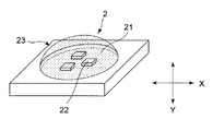
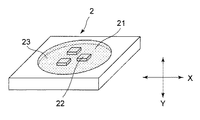
本実施形態では、光源2として、発光素子22をボンディングし、かつ蛍光体を分散させた透明樹脂23で発光素子22を覆うように充填して作られているLEDが採用されている。尚、透明樹脂23が蛍光体層に相当する。このようなLEDのフラットな表面で発光面21が構成されている。例えば、発光面21は、図6Aに示すように円形状であってもよいし、図6Bに示すように四角形状であってもよい。また、図6Cに示すように、発光素子22と、発光素子22上にドーム状に形成され、蛍光体を分散させた透明樹脂23とで構成されていて、透明樹脂23の三次元的な表面で発光面21が構成されていてもよい。
In the present embodiment, as the
また光源2にボンディングする発光素子22は、光源の種類によって異なる個数で構成されていてもよい。このとき発光素子22は、回転対称に配置されていなくてもよい。そのため、本明細書では便宜上、発光面21は、光軸に直交する第1方向と、光軸および第1方向に直交する第2方向とを有し、第1方向をX方向、第2方向をY方向とする。
Moreover, the
光源2の発光面21から放射される光は、発光素子22によって発光した青色の光と、青色の光によって励起された蛍光体からの黄色の光とからなる擬似白色光である。そのため、ニアフィールドにおいて青色と黄色の光の発光面積サイズに差が生じることとなる。また発光素子22の配置によっても分布が変わるため、本明細書では発光素子の配置により分布に異方性がある場合、便宜上青色と黄色の光の発光面積の差が大きい方をX方向、小さい方をY方向と定義する。
The light emitted from the
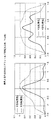
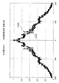
図7に、光源2の発光面21における光軸Aを通ってX方向に延びる線上での輝度分布と、光軸Aを通ってY方向に延びる線上での輝度分布とを、それぞれ色別に示す。尚、図7において、縦軸は、照度を最大値で規格化したものを示し、横軸は、光軸からの距離(mm)を示している。図7に示すように、発光面21において、黄色の光と青色の光との輝度分布の範囲が異なっている。具体的には、黄色の光の輝度分布が青色の光の輝度分布よりも広がっている。このように、光源2からは、光の色によって輝度分布が異なる光が放射される。よって、本実施形態のように疑似白色光を発生する発光装置1が使用される場合には、色ムラを低減する工夫が必要となる。
FIG. 7 shows the luminance distribution on the line extending in the X direction through the optical axis A on the
レンズ3は、所定の屈折率を有する透明材料で構成される。透明材料の屈折率は、例えば1.4から2.0程度である。このような透明材料としては、エポキシ樹脂、シリコン樹脂、アクリル樹脂、ポリカーボネイト等の樹脂、硝子、またはシリコンゴム等のゴムを用いることができる。中でも、従来からLEDの封止樹脂として用いられているエポキシ樹脂またはシリコンゴム等を用いることが好ましい。
The
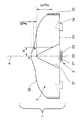
具体的に、レンズ3は、図5Aに示すように、光源2からの光を該レンズ3内に入射させる入射面31と、該レンズ3内に入射した光を出射させる出射面32とを有している。出射面32の最外径は、レンズ3の有効径を規定する。また、レンズ3は、入射面31の周囲に位置し光軸方向において出射面32と反対側に位置する底面33を有している。この底面33には、光軸Aを中心とした円状、あるいは楕円状に反射部34が設けられている。さらに、本実施形態では、出射面32と底面33との間に径方向外側に張り出すリング部35が設けられている。このリング部35の断面形状は、略コ字状で、出射面32の外周縁と底面33の外周縁とがリング部35によってつながれている。ただし、リング部35は省略可能であり、出射面32の外周縁と底面33の外周縁とが断面直線状または円弧状の端面でつながれていてもよい。以下に、レンズ3の上述の各構成部分について、さらに詳しく説明する。
Specifically, as shown in FIG. 5A, the
入射面31は、本実施形態では連続する凹面である。そして、光源2は、レンズ3の入射面31と離れて配置されている。出射面32は、本実施形態では、光軸Aに対して回転対称な連続する凸面である。入射面31を取り巻く環状の底面33は、フラットであることが好ましい。本実施形態では、光源2の発光面21が、フラットな底面33と、光軸Aが延びる光軸方向において同程度の位置にある。
The
光源2からの光は、入射面31からレンズ3内に入射した後に出射面32から出射されて、例えば上述した拡散板4の被照射面4aに到達する。光源2から放射される光は、入射面31および出射面32の屈折作用で拡張され、被照射面4aの広い範囲に到達するようになる。
The light from the
さらに、レンズ3は、上述のように光源2から異なる発光面積で放射される、青色と黄色との光によって生じる被照射面4aでの色ムラを軽減する役割を果たす。これを実現するために、レンズ3は、X方向の屈折力と、Y方向の屈折力とが異なるように構成されている。本実施形態では、入射面31がX方向とY方向とで湾曲態様が異なるアナモフィックな曲面を含むことにより、X方向の屈折力とY方向の屈折力とが異なるようになっている。
Further, the
上述のように本実施形態では入射面31がアナモフィックな曲面を含んで構成しているが、出射面32がアナモフィックな曲面を含むように構成することもできる。つまり、入射面31および出射面32の少なくとも一方がアナモフィックな曲面を含むように構成すればよい。
As described above, in the present embodiment, the
一方、注意すべき点は、上記屈折力とは、光学系の設計や撮像系の設計で一般的に使用されるレンズ「パワー」の概念、つまり非球面レンズならば光軸近傍でのレンズの曲率が異なるという意味ではない。本明細書及び請求範囲で使用する「屈折力」とは、入射面31および出射面32の少なくとも一方は、回転楕円体の表面に相当する形状を有し、光軸Aに直交する断面の形状は、光軸方向におけるいずれの位置にあっても楕円となる、換言するとX方向とY方向とで光軸Aからの距離が異なる、あるいは、光源2からの入射面31および出射面32への入射角が同じ光であってもX方向とY方向とでは入射面31および出射面32からの光の放出方向が異なる、つまり配光方向が異なるという形態を意味する。また、このような形態の曲面を、ここでは「アナモフィック」と称している。
On the other hand, it should be noted that the refractive power is a concept of a lens “power” generally used in optical system design and imaging system design, that is, an aspherical lens. It does not mean that the curvature is different. “Refractive power” used in the present specification and claims means that at least one of the
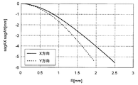
詳細には、図5Aおよび図5Bに示すように、入射面31は、光軸A上に頂点Qを有している。そして、入射面31は、頂点Qから入射面31上の点Pまでの光軸Aに沿った距離(すなわち、光軸方向の距離)をサグ量(符号は頂点Qから光源2側が負、頂点Qから光源2と反対側が正)としたときに、光軸Aから径方向に同じ距離Rだけ離れた位置(すなわち、光軸Aを中心とする同一円周上)では、X方向におけるサグ量sagAXとY方向におけるサグ量sagAYとが異なる、形状を有している。なお、入射面31は、サグ量が光軸Aの近傍ではプラスとなるように頂点Qからいったん光源2の反対側に後退した後に、光源2側に延びていてもよい。
Specifically, as shown in FIGS. 5A and 5B, the
以上のような発光装置1であれば、光源2によって生じる色ムラは、レンズ3によって低減される。従って、相対的に小さなレンズ3を用いながらも、光源2の特性である色ムラを軽減して放射することができる。
In the
以下、本発明の具体的な数値例として、発光装置1の実施例1を示す。
Hereinafter, Example 1 of the light-emitting
図8は、実施例1の発光装置1の断面図である。実施例1は、入射面31の全面がアナモフィックな曲面であり、出射面32が回転対称なレンズ3が採用されている。
FIG. 8 is a cross-sectional view of the
なお、図8中のQ、P、sagAX(sagAY)は、図5Aおよび図5B中に示したものと同じである。また、図8中のsagBは、光軸Aから距離R離れた位置での出射面32のサグ量である。
Note that Q, P, and sagAX (sagAY) in FIG. 8 are the same as those shown in FIGS. 5A and 5B. Further, sagB in FIG. 8 is a sag amount of the
・実施例1
実施例1において、光源2は、発光面21の大きさが、おおよそφ3.0mmの汎用品のLEDを採用し、光源2からの光の方向性を広げ、色ムラを抑えることを目的としている。実施例1において、レンズ3の有効径は、20.7mmとなっている。また、光軸中心でのレンズの厚みが1.2mmとなっている。実施例1の具体的な数値を表1に示す。Example 1
In the first embodiment, the

図9Aは、表1の、X軸、Y軸の値(R)と、sagAXおよびsagAYとについて、グラフ化したものであり、図9Bは、表1の、X軸、Y軸の値(R)と、sagBとについて、グラフ化したものである。 9A is a graph of the values (R) of the X axis and Y axis, sagAX, and sagAY of Table 1, and FIG. 9B is the values of the X axis and Y axis of Table 1 (R). ) And sagB.
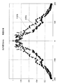
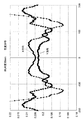
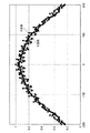
図10は、実施例1の発光装置1を用い、光源2の発光面21から光軸方向において35mm離れた位置に、拡散板4の被照射面4aを配置したときの、被照射面4aでの照度分布を表す。尚、図10において、縦軸は、照度を最大値で規格化したものを示し、横軸は、光軸からの距離(mm)を示している。
FIG. 10 shows the
図11は、実施例1に係る発光装置1の効果を確認するための、レンズ3を用いずに光源2のみで面光源を構成したときの照度分布を表す。
FIG. 11 shows an illuminance distribution when a surface light source is configured by only the
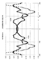
図12は、実施例1と同様の構成の発光装置を用い、光源2の発光面21から光軸方向において35mm離れた位置に、拡散板4の被照射面4a(図示せず)を配置したときの、レンズ3の入射面31を光軸を中心に回転対称の曲面で構成した場合の、被照射面4aでの照度分布を表す。
In FIG. 12, a light emitting device having the same configuration as in Example 1 was used, and an
図13は、実施例1の発光装置1を用い、光源2の発光面21から光軸方向において35mm離れた位置に被照射面4aを配置したときの、被照射面4aでの色度Y値の分布を表す。図13において、縦軸は、照度を最大値で規格化したものを示し、横軸は、光軸からの距離(mm)を示している。
FIG. 13 shows the chromaticity Y value on the
図14は、実施例1と同様の構成の発光装置を用い、光源2の発光面21から光軸方向において35mm離れた位置に被照射面4aを配置したときの、レンズ3の入射面31を光軸を中心に回転対称の曲面で構成した場合の、被照射面4aでの色度Y値の分布を表す。
FIG. 14 shows the
図13と図14とから分かるように、レンズ3の入射面31をアナモフィック非球面にすることにより、被照射面4aにおける色ムラが軽減されていることが確認できる。
As can be seen from FIGS. 13 and 14, it can be confirmed that the color unevenness on the
図15は、実施例1の発光装置1に用いられる、レンズ3の反射部34を無くした場合における、被照射面4aでの照度分布を表す。
FIG. 15 shows the illuminance distribution on the
図10及び図15から分かるように、反射部を設けることで、照射面における光軸近傍の照度を抑えることができ、光源2からの光を効率よく広げることができる。
As can be seen from FIGS. 10 and 15, by providing the reflecting portion, the illuminance near the optical axis on the irradiation surface can be suppressed, and the light from the
また、反射部34と、底面33とのなす角θ(図5A、図5B)は、15°<θ<45°が好ましい。15°以下になると被照射面4aの光軸近傍における照度を抑える効果が小さくなり、45°以上になると、光源2から出射した光が直接反射部34にあたり、被照射面4aでの照度ムラの原因となる。
Further, it is preferable that the angle θ (FIGS. 5A and 5B) formed by the reflecting
また、反射部34は、光軸Aから、レンズ3の有効径の65%以上の外側に位置することが望ましい。これは、出射面32側で反射した光が底面33の外側に集中することから、これらの光を効率的に出射面32側へ反射させるためであり、光軸Aに近い位置に設けても効果が少ないためである。
Further, it is desirable that the reflecting
図16は、入射面31がアナモフィックな曲面であるレンズ3を採用した実施例1の発光装置1を60mmピッチで一直線上に5つ配置し、光源2の発光面21から光軸方向において35mm離れた位置に拡散板4を配置したときの、計算で求めた拡散板4の被照射面4aでの照度分布を表す。照度分布に細かな波が見られるのは、照度計算を実行する上で、評価する光線数が不足しているためである。
In FIG. 16, five light emitting
図17は、レンズ3を用いずに光源2のみを60mmピッチで一直線上に5つ配置し、LED光源2の表面から光軸方向において35mm離れた位置に拡散板4を配置したときの、計算で求めた拡散板4の被照射面4aでの照度分布を表す。
FIG. 17 shows a calculation when only five
図16と図17とを比較すると、図16よりレンズ3の効果で拡散板4の被照射面4aを均一に照明できていることがわかる。
16 is compared with FIG. 17, it can be seen from FIG. 16 that the
なお、上記様々な実施形態のうちの任意の実施形態を適宜組み合わせることにより、それぞれの有する効果を奏するようにすることができる。
本発明は、添付図面を参照しながら好ましい実施形態に関連して充分に記載されているが、この技術の熟練した人々にとっては種々の変形や修正は明白である。そのような変形や修正は、添付した請求の範囲による本発明の範囲から外れない限りにおいて、その中に含まれると理解されるべきである。
又、2011年5月31日に出願された、日本国特許出願No.特願2011−121373号の明細書、図面、特許請求の範囲、及び要約書の開示内容の全ては、参考として本明細書中に編入されるものである。It is to be noted that, by appropriately combining arbitrary embodiments of the various embodiments described above, the effects possessed by them can be produced.
Although the present invention has been fully described in connection with preferred embodiments with reference to the accompanying drawings, various variations and modifications will be apparent to those skilled in the art. Such changes and modifications are to be understood as being included therein, so long as they do not depart from the scope of the present invention according to the appended claims.
In addition, Japanese Patent Application No. 1 filed on May 31, 2011 was submitted. The entire contents of the specification, drawings, claims, and abstract of Japanese Patent Application No. 2011-121373 are incorporated herein by reference.
以上のように本発明によれば、色ムラの少ない十分な明るさの面光源を提供する上で有用な発明である。 As described above, according to the present invention, the invention is useful in providing a surface light source with sufficient brightness with little color unevenness.
1 発光装置
2 光源
3 レンズ
4 拡散板
5 基板
6 反射シート ないし 反射コーティング膜
7 面光源
8 液晶表示パネル
21 発光面
22 発光素子
23 蛍光体を分散させた透明樹脂
31 入射面
32 出射面
33 底面
34 反射部
35 リング部DESCRIPTION OF
本発明は、例えば発光ダイオード(以下単に「LED」という。)等の光源からの光の方向性をレンズで広げる発光装置に関する。また、本発明は、この発光装置を複数備える面光源、およびこの面光源がバックライトとして液晶表示パネル後方に配置された液晶ディスプレイ装置、さらに、発光装置に備わるレンズに関する。 The present invention relates to a light emitting device that spreads the directionality of light from a light source such as a light emitting diode (hereinafter simply referred to as “LED”) with a lens. The present invention also relates to a surface light source including a plurality of the light emitting devices, a liquid crystal display device in which the surface light sources are arranged behind the liquid crystal display panel as a backlight, and a lens provided in the light emitting device.
従来の大型の液晶ディスプレイ装置のバックライトでは、冷陰極管が液晶表示パネル直下に多数配置され、これらの冷陰極管が拡散板や反射板等の部材と共に使われていた。近年では、バックライトの光源としてLEDが使用されるようになっている。LEDは、近年、発光効率が向上し、蛍光灯に変わる消費電力の少ない光源として期待されている。また液晶ディスプレイ装置用の光源としては映像に応じてLEDの明暗を制御することで液晶ディスプレイ装置の消費電力を下げることができる。 In the backlight of a conventional large-sized liquid crystal display device, a large number of cold cathode tubes are arranged directly under the liquid crystal display panel, and these cold cathode tubes are used together with members such as a diffusion plate and a reflector. In recent years, LEDs have been used as light sources for backlights. In recent years, LEDs have been expected as light sources with improved luminous efficiency and low power consumption, replacing fluorescent lamps. Further, as a light source for a liquid crystal display device, the power consumption of the liquid crystal display device can be reduced by controlling the brightness of the LED according to the image.
液晶ディスプレイ装置において、LEDを光源とするバックライトでは、冷陰極管の代わりに多数のLEDを配置することとなる。多数のLEDを用いることでバックライト表面に均一な明るさを得ることができるが、多数のLEDが必要なことから、安価にできない問題があった。この欠点を解決すべく、1個のLEDの出力を大きくし、使用するLEDの個数を減らす取り組みがなされている。例えば特許文献1では、少ない個数のLEDでも均一な輝度の面光源が得られるようにする発光装置が提案されている。
In a liquid crystal display device, in a backlight using LEDs as light sources, a large number of LEDs are arranged instead of cold cathode tubes. By using a large number of LEDs, a uniform brightness can be obtained on the surface of the backlight. However, since a large number of LEDs are required, there is a problem that the cost cannot be reduced. In order to solve this drawback, efforts have been made to increase the output of one LED and reduce the number of LEDs used. For example,
少ない個数のLEDで均一な輝度の面光源を得るためには、1個のLEDで照明可能な照明領域を大きくする必要がある。このために特許文献1の発光装置では、LEDからの光をレンズで放射状に拡張している。これにより、LEDからの光の方向性が広げられ、被照射面において、LEDの光軸を中心とする広い範囲を照明することができる。具体的に、特許文献1の発光装置に用いられるレンズは、平面視で円形状をなしており、光入射面と光制御出射面とが共に光軸に対して回転対称な形状である。ここで、光入射面は、凹面にて形成され、光制御出射面は、光軸近傍部分が凹面で光軸近傍部分の外側部分が凸面にて形成されている。
In order to obtain a surface light source having a uniform luminance with a small number of LEDs, it is necessary to enlarge an illumination area that can be illuminated with one LED. For this reason, in the light emitting device of
一方、特許文献2には、光出射面の中央に、光軸と直交する方向に延びるV溝が形成されたレンズを用いた発光装置が開示されている。この発光装置のレンズによれば、LEDからの光は、V溝が延びる方向(縦方向)には、正規分布の角度分布を保ったまま拡張されるが、V溝が延びる方向と直交する方向(横方向)には、角度分布が光軸近傍では大きく窪み、その両側では急峻に立ち上がるように拡張される。
On the other hand,
近年の白色LEDは、青色LED素子に、YAG系やTAG系などの蛍光体を設けて、疑似白色光を生成するものが主流となっている。このような光源は、パッケージに青色LED素子をボンディングし、青色LED素子を覆うように蛍光体を分散させた透明樹脂を充填して作られている。 In recent years, white LEDs are mainly used in which a blue LED element is provided with a phosphor such as YAG or TAG to generate pseudo white light. Such a light source is made by bonding a blue LED element to a package and filling a transparent resin in which a phosphor is dispersed so as to cover the blue LED element.
このような光源は、青色LED素子による青色の光と、青色の光により励起された蛍光体が発光して作る黄色の光とで擬似白色の光を得ているため、青色の発光面サイズと、黄色の発光面のサイズとが異なる。そのため、このようなLEDの光を、特許文献1にあるようなレンズを用いて広げた場合、色によって光の広がりに差が生じ、光源からの光が照射される面光源内の被照射面において色ムラが生じてしまうことになる。またこの色ムラは、光を広げるパワーが強いレンズほど顕著になる傾向にある。
Such a light source obtains pseudo-white light from blue light produced by a blue LED element and yellow light produced by a phosphor excited by blue light, and therefore has a blue light emitting surface size. The size of the yellow light emitting surface is different. Therefore, when such LED light is spread using a lens as in
LEDの発光効率が向上しつつある近年においては、光源1つあたりの、上記被照射面における照射面積を広げ、なおかつ、輝度及び色が共に均一化された、低コストで省エネルギーの発光装置が望まれる。 In recent years when the luminous efficiency of LEDs is improving, a low-cost and energy-saving light-emitting device is desired in which the irradiation area per surface of the light source is increased on the surface to be irradiated and the luminance and color are both uniform. It is.
なお、特許文献2の発光装置は、放射する光に意図的に異方性を作り出すものであるため、上述の要望を満たすものではない。
In addition, since the light-emitting device of
本発明は、上述の要望に鑑み、光を広げる力がある広配光レンズを用いながら、光源が持っている異なる色の光によって生じる被照射面の色ムラを軽減することができ、輝度及び色が共に均一化された発光装置を提供するとともに、この発光装置を含む面光源、および液晶ディスプレイ装置、さらに発光装置に備わるレンズを提供することを目的とする。 In view of the above-described demand, the present invention can reduce unevenness in color of an irradiated surface caused by light of different colors possessed by a light source while using a wide light distribution lens that has the ability to spread light. It is an object of the present invention to provide a light-emitting device in which both colors are uniform, and to provide a surface light source including the light-emitting device, a liquid crystal display device, and a lens included in the light-emitting device.
上記目的を達成するため、本発明は以下のように構成する。
即ち、本発明の第1態様における発光装置は、光軸を中心として光を放射する発光装置であって、発光素子、および前記発光素子を覆い蛍光体を分散させた樹脂を有する光源と、前記光源からの光を放射状に拡張するレンズとを備え、前記レンズは、前記光軸と直交する第1方向と、前記光軸および前記第1方向に直交する第2方向との屈折力が異なる。
In order to achieve the above object, the present invention is configured as follows.
That is, the light-emitting device according to the first aspect of the present invention is a light-emitting device that emits light around the optical axis, the light-emitting element, and a light source that covers the light-emitting element and has a resin in which a phosphor is dispersed; A lens that radially expands light from the light source, and the lens has different refractive powers in a first direction orthogonal to the optical axis and in a second direction orthogonal to the optical axis and the first direction.
また、本発明の第2態様における面光源は、平面的に配置された複数の発光装置と、前記複数の発光装置を覆うように配置され、前記複数の発光装置から被照射面に照射された光を放射面から拡散した状態で放射する拡散板と、を備える面光源であって、前記複数の発光装置のそれぞれは、上述の第1態様における発光装置である。 Moreover, the surface light source in the 2nd aspect of this invention is arrange | positioned so that the several light-emitting device arrange | positioned planarly and the said several light-emitting device may be covered, and the to-be-irradiated surface was irradiated from the said several light-emitting device Each of the plurality of light-emitting devices is the light-emitting device according to the first aspect described above.
さらに、本発明の第3態様における液晶ディスプレイ装置は、液晶表示パネルと、前記液晶表示パネルの裏側に配置された上述の第2態様における面光源と、を備える。 Furthermore, a liquid crystal display device according to a third aspect of the present invention includes a liquid crystal display panel and the surface light source according to the second aspect described above disposed on the back side of the liquid crystal display panel.
さらに、本発明の第4態様におけるレンズは、発光ダイオードからの光を拡張するレンズであって、光軸を中心として発光ダイオードからの光が入射する入射面と、入射した光を放射状に拡張して出射する出射面と、を有し、入射面は、連続する凹面を有し、出射面は、連続する凸面を有し、かつ前記レンズは、前記入射面および前記出射面の少なくとも一方において、光軸に直交する第1方向と、前記光軸および前記第1方向に直交する第2方向との屈折力が異なるように構成した。 Further, the lens according to the fourth aspect of the present invention is a lens that expands light from the light emitting diode, and has an incident surface on which the light from the light emitting diode is incident with the optical axis as a center, and the incident light is radially expanded. And the exit surface has a continuous concave surface, the exit surface has a continuous convex surface, and at least one of the entrance surface and the exit surface, The first direction perpendicular to the optical axis and the second direction perpendicular to the optical axis and the first direction are configured to have different refractive powers.
上述の第1態様における発光装置によれば、光軸と直交する第1方向のレンズの屈折力と、光軸および第1方向に直交する第2方向のレンズの屈折力とが異なることで、レンズの出射面側で生じる光の全反射成分が低減される。従って、本発明の第1態様における発光装置によれば、光を広げるパワーの強いレンズを用いながらも、光源が持っている色の異なる光によって生じる被照射面の色ムラを軽減することができ、輝度及び色が共に均一化された発光装置を提供することができる。さらに、この発光装置を含む第2態様の面光源、および第3態様の液晶ディスプレイ装置においても、被照射面の色ムラを軽減することができ、輝度及び色が共に均一化できる。さらにまた、第4態様のレンズにおいても、入射面および出射面の少なくとも一方における第1方向のレンズの屈折力と、第2方向のレンズの屈折力とが異なることから、被照射面の色ムラを軽減することができ、輝度及び色が共に均一化できる。 According to the light emitting device in the first aspect described above, the refractive power of the lens in the first direction orthogonal to the optical axis is different from the refractive power of the lens in the second direction orthogonal to the optical axis and the first direction. The total reflection component of light generated on the exit surface side of the lens is reduced. Therefore, according to the light emitting device of the first aspect of the present invention, it is possible to reduce color unevenness on the irradiated surface caused by light of different colors that the light source has while using a lens with high power that spreads light. Further, it is possible to provide a light emitting device in which both luminance and color are uniform. Further, in the surface light source of the second aspect including the light emitting device and the liquid crystal display device of the third aspect, color unevenness on the irradiated surface can be reduced, and both luminance and color can be made uniform. Furthermore, in the lens of the fourth aspect, since the refractive power of the lens in the first direction and the refractive power of the lens in the second direction on at least one of the entrance surface and the exit surface are different, color unevenness on the irradiated surface. Can be reduced, and both luminance and color can be made uniform.
以下、本発明の一実施の形態による発光装置、およびその発光装置を用いた面光源、およびその面光源を用いた液晶ディスプレイ装置について、図面を参照しながら説明する。尚、各図において、同一又は同様の構成部分については同じ符号を付している。 Hereinafter, a light emitting device according to an embodiment of the present invention, a surface light source using the light emitting device, and a liquid crystal display device using the surface light source will be described with reference to the drawings. In each figure, the same or similar components are denoted by the same reference numerals.
(実施の形態1)
図1は、本発明の実施の形態1に係る液晶ディスプレイ装置101の全体の概略構成を示す図である。この液晶ディスプレイ装置101は、液晶表示パネル8と、液晶表示パネル8の裏側(反表示面側)に配置された面光源7とを備えている。面光源7は、発光装置1と、発光装置1に対向して設置される拡散板4とを有する。尚、面光源7については、以下の実施の形態2にて詳しく説明する。
(Embodiment 1)
FIG. 1 is a diagram showing an overall schematic configuration of a liquid
複数の発光装置1は、拡散板4に対向して平面的に分散して配置され、これらの発光装置1によって、拡散板4の、発光装置1に対向する裏面(被照射面)は、照度が均一化された光で照射される。この光が拡散板4によって拡散されて、拡散板4の表面(照射面)から出射され、液晶表示パネル8が照明される。
The plurality of light emitting
なお、液晶表示パネル8と面光源7との間には拡散シート、プリズムシート等の光学シートが配置されていることが好ましい。この場合、拡散板4を透過した光は、光学シートでさらに拡散されて、液晶表示パネル8を照明する。
An optical sheet such as a diffusion sheet or a prism sheet is preferably disposed between the liquid
(実施の形態2)
ここでは、本発明の実施の形態2に係る面光源7について、詳しく説明する。図2は、面光源7の構成図である。この面光源7は、上述したように、複数の発光装置1と、これらの発光装置1を覆うように配置される拡散板4とを備えている。発光装置1は、光源2と光源2を覆って配置されるレンズ3とを有する。拡散板4は、光源2の光軸に対して直交方向に延在する。また、発光装置1は、筐体内の底部に配置され、底部に対向する筐体の開口部を拡散板4で閉止して、面光源7が形成される。なお、発光装置1は、拡散板4の全面又は略全面に対向して平面的に分散して配置されていればよく、図2に示すように、マトリクス状に配置されていてもよいし、千鳥状に配置されていてもよく、その配置形態を問わない。
発光装置1を構成する光源2およびレンズ3については、以下の実施の形態3にて詳しく説明する。
(Embodiment 2)
Here, the
The
また、面光源7は、図3に示すように、発光装置1を挟んで拡散板4と対向する基板5を備えている。基板5には、各発光装置1の光源2が実装されている。本実施形態では、レンズ3の底面33が基板5に支柱55を介して接合されている。さらに基板5上には、光源2を避けながら基板5を覆うように、つまり光源2を露出させながら基板5を覆うように反射シート6が配置されているか、基板5に反射シート6に代わる反射コーティングがされている。尚、反射シート6および反射コーティングは、反射用部材の一例に相当する。また、レンズ3の底面33は、必ずしも基板5に支柱55を介して接合されている必要はなく、基板5に直接的に接合されていてもよい。また、支柱55が、レンズ3と一体で形成されていてもよい。
Further, as shown in FIG. 3, the
発光装置1は、拡散板4の被照射面4aに光を照射する。拡散板4は、被照射面4aに照射された光を放射面4bから拡散された状態で放射する。個々の発光装置1からは拡散板4の被照射面4aに広い範囲で均一化された照度の光が照射され、この光が拡散板4で拡散されることにより、面内での輝度ムラが少ない面光源7が達成できる。尚、発光装置1から、色ムラが軽減され、輝度及び色が共に均一化された光が照射可能となるメカニズムについては、以下の実施の形態3にて説明する。
The
発光装置1からの光は、拡散板4で散乱されて、発光装置1側へ戻ったり拡散板4を透過したりする。発光装置1側へ戻って反射シート6に入射する光は、反射シート6で反射されて、拡散板4に再度入射する。
Light from the
(実施の形態3)
ここでは、本発明の実施の形態3に係る発光装置1について、詳しく説明する。図4ならびに図5Aおよび5Bに、発光装置1の構成を示す。この発光装置1は、既に説明したように、光源2と、光源2からの光を放射状に拡張するレンズ3とを備え、例えば拡散板4の被照射面4aに、光軸Aを中心として略円形状に光を放射するものである。すなわち、光源2からの光の方向性がレンズ3で広げられ、これにより拡散板4の被照射面4aにおける光軸Aを中心とする広い範囲が照明される。被照射面4aの照度分布は、光軸A上が最大で、周囲に行くほど略単調に減少する。
(Embodiment 3)
Here, the
本実施形態では、光源2として、発光素子22をボンディングし、かつ蛍光体を分散させた透明樹脂23で発光素子22を覆うように充填して作られているLEDが採用されている。尚、透明樹脂23が蛍光体層に相当する。このようなLEDのフラットな表面で発光面21が構成されている。例えば、発光面21は、図6Aに示すように円形状であってもよいし、図6Bに示すように四角形状であってもよい。また、図6Cに示すように、発光素子22と、発光素子22上にドーム状に形成され、蛍光体を分散させた透明樹脂23とで構成されていて、透明樹脂23の三次元的な表面で発光面21が構成されていてもよい。
In the present embodiment, as the
また光源2にボンディングする発光素子22は、光源の種類によって異なる個数で構成されていてもよい。このとき発光素子22は、回転対称に配置されていなくてもよい。そのため、本明細書では便宜上、発光面21は、光軸に直交する第1方向と、光軸および第1方向に直交する第2方向とを有し、第1方向をX方向、第2方向をY方向とする。
Moreover, the
光源2の発光面21から放射される光は、発光素子22によって発光した青色の光と、青色の光によって励起された蛍光体からの黄色の光とからなる擬似白色光である。そのため、ニアフィールドにおいて青色と黄色の光の発光面積サイズに差が生じることとなる。また発光素子22の配置によっても分布が変わるため、本明細書では発光素子の配置により分布に異方性がある場合、便宜上青色と黄色の光の発光面積の差が大きい方をX方向、小さい方をY方向と定義する。
The light emitted from the
図7に、光源2の発光面21における光軸Aを通ってX方向に延びる線上での輝度分布と、光軸Aを通ってY方向に延びる線上での輝度分布とを、それぞれ色別に示す。尚、図7において、縦軸は、照度を最大値で規格化したものを示し、横軸は、光軸からの距離(mm)を示している。図7に示すように、発光面21において、黄色の光と青色の光との輝度分布の範囲が異なっている。具体的には、黄色の光の輝度分布が青色の光の輝度分布よりも広がっている。このように、光源2からは、光の色によって輝度分布が異なる光が放射される。よって、本実施形態のように疑似白色光を発生する発光装置1が使用される場合には、色ムラを低減する工夫が必要となる。
FIG. 7 shows the luminance distribution on the line extending in the X direction through the optical axis A on the
レンズ3は、所定の屈折率を有する透明材料で構成される。透明材料の屈折率は、例えば1.4から2.0程度である。このような透明材料としては、エポキシ樹脂、シリコン樹脂、アクリル樹脂、ポリカーボネイト等の樹脂、硝子、またはシリコンゴム等のゴムを用いることができる。中でも、従来からLEDの封止樹脂として用いられているエポキシ樹脂またはシリコンゴム等を用いることが好ましい。
The
具体的に、レンズ3は、図5Aに示すように、光源2からの光を該レンズ3内に入射させる入射面31と、該レンズ3内に入射した光を出射させる出射面32とを有している。出射面32の最外径は、レンズ3の有効径を規定する。また、レンズ3は、入射面31の周囲に位置し光軸方向において出射面32と反対側に位置する底面33を有している。この底面33には、光軸Aを中心とした円状、あるいは楕円状に反射部34が設けられている。さらに、本実施形態では、出射面32と底面33との間に径方向外側に張り出すリング部35が設けられている。このリング部35の断面形状は、略コ字状で、出射面32の外周縁と底面33の外周縁とがリング部35によってつながれている。ただし、リング部35は省略可能であり、出射面32の外周縁と底面33の外周縁とが断面直線状または円弧状の端面でつながれていてもよい。以下に、レンズ3の上述の各構成部分について、さらに詳しく説明する。
Specifically, as shown in FIG. 5A, the
入射面31は、本実施形態では連続する凹面である。そして、光源2は、レンズ3の入射面31と離れて配置されている。出射面32は、本実施形態では、光軸Aに対して回転対称な連続する凸面である。入射面31を取り巻く環状の底面33は、フラットであることが好ましい。本実施形態では、光源2の発光面21が、フラットな底面33と、光軸Aが延びる光軸方向において同程度の位置にある。
The
光源2からの光は、入射面31からレンズ3内に入射した後に出射面32から出射されて、例えば上述した拡散板4の被照射面4aに到達する。光源2から放射される光は、入射面31および出射面32の屈折作用で拡張され、被照射面4aの広い範囲に到達するようになる。
The light from the
さらに、レンズ3は、上述のように光源2から異なる発光面積で放射される、青色と黄色との光によって生じる被照射面4aでの色ムラを軽減する役割を果たす。これを実現するために、レンズ3は、X方向の屈折力と、Y方向の屈折力とが異なるように構成されている。本実施形態では、入射面31がX方向とY方向とで湾曲態様が異なるアナモフィックな曲面を含むことにより、X方向の屈折力とY方向の屈折力とが異なるようになっている。
Further, the
上述のように本実施形態では入射面31がアナモフィックな曲面を含んで構成しているが、出射面32がアナモフィックな曲面を含むように構成することもできる。つまり、入射面31および出射面32の少なくとも一方がアナモフィックな曲面を含むように構成すればよい。
As described above, in the present embodiment, the
一方、注意すべき点は、上記屈折力とは、光学系の設計や撮像系の設計で一般的に使用されるレンズ「パワー」の概念、つまり非球面レンズならば光軸近傍でのレンズの曲率が異なるという意味ではない。本明細書及び請求範囲で使用する「屈折力」とは、入射面31および出射面32の少なくとも一方は、回転楕円体の表面に相当する形状を有し、光軸Aに直交する断面の形状は、光軸方向におけるいずれの位置にあっても楕円となる、換言するとX方向とY方向とで光軸Aからの距離が異なる、あるいは、光源2からの入射面31および出射面32への入射角が同じ光であってもX方向とY方向とでは入射面31および出射面32からの光の放出方向が異なる、つまり配光方向が異なるという形態を意味する。また、このような形態の曲面を、ここでは「アナモフィック」と称している。
On the other hand, it should be noted that the refractive power is a concept of a lens “power” generally used in optical system design and imaging system design, that is, an aspherical lens. It does not mean that the curvature is different. “Refractive power” used in the present specification and claims means that at least one of the
詳細には、図5Aおよび図5Bに示すように、入射面31は、光軸A上に頂点Qを有している。そして、入射面31は、頂点Qから入射面31上の点Pまでの光軸Aに沿った距離(すなわち、光軸方向の距離)をサグ量(符号は頂点Qから光源2側が負、頂点Qから光源2と反対側が正)としたときに、光軸Aから径方向に同じ距離Rだけ離れた位置(すなわち、光軸Aを中心とする同一円周上)では、X方向におけるサグ量sagAXとY方向におけるサグ量sagAYとが異なる、形状を有している。なお、入射面31は、サグ量が光軸Aの近傍ではプラスとなるように頂点Qからいったん光源2の反対側に後退した後に、光源2側に延びていてもよい。
Specifically, as shown in FIGS. 5A and 5B, the
以上のような発光装置1であれば、光源2によって生じる色ムラは、レンズ3によって低減される。従って、相対的に小さなレンズ3を用いながらも、光源2の特性である色ムラを軽減して放射することができる。
In the
以下、本発明の具体的な数値例として、発光装置1の実施例1を示す。
Hereinafter, Example 1 of the light-emitting
図8は、実施例1の発光装置1の断面図である。実施例1は、入射面31の全面がアナモフィックな曲面であり、出射面32が回転対称なレンズ3が採用されている。
FIG. 8 is a cross-sectional view of the
なお、図8中のQ、P、sagAX(sagAY)は、図5Aおよび図5B中に示したものと同じである。また、図8中のsagBは、光軸Aから距離R離れた位置での出射面32のサグ量である。
Note that Q, P, and sagAX (sagAY) in FIG. 8 are the same as those shown in FIGS. 5A and 5B. Further, sagB in FIG. 8 is a sag amount of the
・実施例1
実施例1において、光源2は、発光面21の大きさが、おおよそφ3.0mmの汎用品のLEDを採用し、光源2からの光の方向性を広げ、色ムラを抑えることを目的としている。実施例1において、レンズ3の有効径は、20.7mmとなっている。また、光軸中心でのレンズの厚みが1.2mmとなっている。実施例1の具体的な数値を表1に示す。
Example 1
In the first embodiment, the
図9Aは、表1の、X軸、Y軸の値(R)と、sagAXおよびsagAYとについて、グラフ化したものであり、図9Bは、表1の、X軸、Y軸の値(R)と、sagBとについて、グラフ化したものである。 9A is a graph of the values (R) of the X axis and Y axis, sagAX, and sagAY of Table 1, and FIG. 9B is the values of the X axis and Y axis of Table 1 (R). ) And sagB.
図10は、実施例1の発光装置1を用い、光源2の発光面21から光軸方向において35mm離れた位置に、拡散板4の被照射面4aを配置したときの、被照射面4aでの照度分布を表す。尚、図10において、縦軸は、照度を最大値で規格化したものを示し、横軸は、光軸からの距離(mm)を示している。
FIG. 10 shows the
図11は、実施例1に係る発光装置1の効果を確認するための、レンズ3を用いずに光源2のみで面光源を構成したときの照度分布を表す。
FIG. 11 shows an illuminance distribution when a surface light source is configured by only the
図12は、実施例1と同様の構成の発光装置を用い、光源2の発光面21から光軸方向において35mm離れた位置に、拡散板4の被照射面4a(図示せず)を配置したときの、レンズ3の入射面31を光軸を中心に回転対称の曲面で構成した場合の、被照射面4aでの照度分布を表す。
In FIG. 12, a light emitting device having the same configuration as in Example 1 was used, and an
図13は、実施例1の発光装置1を用い、光源2の発光面21から光軸方向において35mm離れた位置に被照射面4aを配置したときの、被照射面4aでの色度Y値の分布を表す。図13において、縦軸は、照度を最大値で規格化したものを示し、横軸は、光軸からの距離(mm)を示している。
FIG. 13 shows the chromaticity Y value on the
図14は、実施例1と同様の構成の発光装置を用い、光源2の発光面21から光軸方向において35mm離れた位置に被照射面4aを配置したときの、レンズ3の入射面31を光軸を中心に回転対称の曲面で構成した場合の、被照射面4aでの色度Y値の分布を表す。
FIG. 14 shows the
図13と図14とから分かるように、レンズ3の入射面31をアナモフィック非球面にすることにより、被照射面4aにおける色ムラが軽減されていることが確認できる。
As can be seen from FIGS. 13 and 14, it can be confirmed that the color unevenness on the
図15は、実施例1の発光装置1に用いられる、レンズ3の反射部34を無くした場合における、被照射面4aでの照度分布を表す。
FIG. 15 shows the illuminance distribution on the
図10及び図15から分かるように、反射部を設けることで、照射面における光軸近傍の照度を抑えることができ、光源2からの光を効率よく広げることができる。
As can be seen from FIGS. 10 and 15, by providing the reflecting portion, the illuminance near the optical axis on the irradiation surface can be suppressed, and the light from the
また、反射部34と、底面33とのなす角θ(図5A、図5B)は、15°<θ<45°が好ましい。15°以下になると被照射面4aの光軸近傍における照度を抑える効果が小さくなり、45°以上になると、光源2から出射した光が直接反射部34にあたり、被照射面4aでの照度ムラの原因となる。
Further, it is preferable that the angle θ (FIGS. 5A and 5B) formed by the reflecting
また、反射部34は、光軸Aから、レンズ3の有効径の65%以上の外側に位置することが望ましい。これは、出射面32側で反射した光が底面33の外側に集中することから、これらの光を効率的に出射面32側へ反射させるためであり、光軸Aに近い位置に設けても効果が少ないためである。
Further, it is desirable that the reflecting
図16は、入射面31がアナモフィックな曲面であるレンズ3を採用した実施例1の発光装置1を60mmピッチで一直線上に5つ配置し、光源2の発光面21から光軸方向において35mm離れた位置に拡散板4を配置したときの、計算で求めた拡散板4の被照射面4aでの照度分布を表す。照度分布に細かな波が見られるのは、照度計算を実行する上で、評価する光線数が不足しているためである。
In FIG. 16, five light emitting
図17は、レンズ3を用いずに光源2のみを60mmピッチで一直線上に5つ配置し、LED光源2の表面から光軸方向において35mm離れた位置に拡散板4を配置したときの、計算で求めた拡散板4の被照射面4aでの照度分布を表す。
FIG. 17 shows a calculation when only five
図16と図17とを比較すると、図16よりレンズ3の効果で拡散板4の被照射面4aを均一に照明できていることがわかる。
16 is compared with FIG. 17, it can be seen from FIG. 16 that the
なお、上記様々な実施形態のうちの任意の実施形態を適宜組み合わせることにより、それぞれの有する効果を奏するようにすることができる。
本発明は、添付図面を参照しながら好ましい実施形態に関連して充分に記載されているが、この技術の熟練した人々にとっては種々の変形や修正は明白である。そのような変形や修正は、添付した請求の範囲による本発明の範囲から外れない限りにおいて、その中に含まれると理解されるべきである。
又、2011年5月31日に出願された、日本国特許出願No.特願2011−121373号の明細書、図面、特許請求の範囲、及び要約書の開示内容の全ては、参考として本明細書中に編入されるものである。
It is to be noted that, by appropriately combining arbitrary embodiments of the various embodiments described above, the effects possessed by them can be produced.
Although the present invention has been fully described in connection with preferred embodiments with reference to the accompanying drawings, various variations and modifications will be apparent to those skilled in the art. Such changes and modifications are to be understood as being included therein, so long as they do not depart from the scope of the present invention according to the appended claims.
In addition, Japanese Patent Application No. 1 filed on May 31, 2011 was submitted. The entire contents of the specification, drawings, claims, and abstract of Japanese Patent Application No. 2011-121373 are incorporated herein by reference.
以上のように本発明によれば、色ムラの少ない十分な明るさの面光源を提供する上で有用な発明である。 As described above, according to the present invention, the invention is useful in providing a surface light source with sufficient brightness with little color unevenness.
1 発光装置
2 光源
3 レンズ
4 拡散板
5 基板
6 反射シート ないし 反射コーティング膜
7 面光源
8 液晶表示パネル
21 発光面
22 発光素子
23 蛍光体を分散させた透明樹脂
31 入射面
32 出射面
33 底面
34 反射部
35 リング部
DESCRIPTION OF
Claims (18)
前記レンズは、光軸を中心として光源からの光が入射する入射面(31)と、入射した光を放射状に拡張して出射する出射面(32)と、を有し、
前記入射面は、連続する凹面を有し、前記出射面は、連続する凸面を有し、かつ前記レンズは、前記光軸に直交する第1方向と、前記光軸および前記第1方向に直交する第2方向との屈折力が異なる、
発光装置。In a light emitting device (1) having a light source (2) and a lens (3) arranged over the light source and extending light from the light source,
The lens has an incident surface (31) on which light from a light source is incident with an optical axis as a center, and an exit surface (32) that radially expands and emits the incident light.
The incident surface has a continuous concave surface, the output surface has a continuous convex surface, and the lens is orthogonal to the first direction orthogonal to the optical axis, and to the optical axis and the first direction. The refractive power of the second direction is different,
Light emitting device.
前記底面には、光軸に沿って凹形状の反射部(34)を有する、請求項1に記載の発光装置。The lens further includes a bottom surface (33) positioned around the entrance surface and located on the opposite side of the exit surface;
The light-emitting device according to claim 1, wherein the bottom surface includes a concave reflecting portion (34) along the optical axis.
前記出射面は、前記光軸に対して回転対称な凸面である、請求項3に記載の発光装置。The incident surface is a concave surface including an anamorphic aspherical curved surface having different refractive powers in the first direction and the second direction,
The light emitting device according to claim 3, wherein the emission surface is a convex surface that is rotationally symmetric with respect to the optical axis.
15°<θ<45°
を満足する、請求項3に記載の発光装置。The angle θ formed with the bottom surface of the reflecting portion is the following conditional expression:
15 ° <θ <45 °
The light emitting device according to claim 3, wherein:
前記発光装置に対向して配置され光源の光軸に直交して延在する拡散板(4)と、
前記発光装置から出射した光を前記拡散板側に反射させる反射用部材(6)と、
を備え、
前記レンズは、光源の光軸に直交する第1方向と、前記光軸および前記第1方向に直交する第2方向との屈折力が異なり、
複数個の前記発光装置は、前記拡散板に対向して分散して配置される、
面光源。A plurality of light emitting devices (1) having a light source (2) and a lens (3) disposed over the light source and extending the light from the light source;
A diffusion plate (4) disposed opposite to the light emitting device and extending perpendicular to the optical axis of the light source;
A reflecting member (6) for reflecting light emitted from the light emitting device toward the diffuser plate;
With
The lens has different refractive powers in a first direction orthogonal to the optical axis of the light source and a second direction orthogonal to the optical axis and the first direction,
A plurality of the light emitting devices are arranged so as to be opposed to the diffusion plate.
Surface light source.
前記面光源は、複数個の前記発光装置を、前記拡散板に対向して分散させて配置し、
前記発光装置のレンズは、光軸を中心として光源からの光が入射する入射面(31)と、入射した光を放射状に拡張して出射する出射面(32)と、を有し、
前記入射面は、連続する凹面を有し、前記出射面は、連続する凸面を有し、かつ前記レンズは、前記入射面および前記出射面の少なくとも一方において、前記光軸に直交する第1方向と、前記光軸および前記第1方向に直交する第2方向との屈折力が異なる、
液晶ディスプレイ装置。A liquid crystal display device comprising a liquid crystal display panel (8) and a surface light source (7) disposed on the back side of the liquid crystal display panel and having a size corresponding to the liquid crystal display panel, wherein the surface light source is A light emitting device (1) having a plurality of light sources (2) and a lens (3) arranged to cover the light sources and extending light from the light sources, and disposed adjacent to the liquid crystal display panel so as to face the light emitting devices A liquid crystal display device (101) comprising: a diffusion plate (4) extending perpendicular to the optical axis of the light source; and a reflection member (6) for reflecting the light emitted from the light emitting device toward the diffusion plate. )
The surface light source includes a plurality of the light emitting devices arranged to be opposed to the diffusion plate,
The lens of the light emitting device has an incident surface (31) on which light from a light source is incident with an optical axis as a center, and an output surface (32) that radially expands and emits the incident light.
The entrance surface has a continuous concave surface, the exit surface has a continuous convex surface, and the lens has a first direction orthogonal to the optical axis in at least one of the entrance surface and the exit surface. And the refractive power of the second direction orthogonal to the optical axis and the first direction is different,
Liquid crystal display device.
前記レンズは、光軸を中心として発光ダイオードからの光が入射する入射面(31)と、入射した光を放射状に拡張して出射する出射面(32)と、を有し、
前記入射面は、連続する凹面を有し、前記出射面は、連続する凸面を有し、かつ前記レンズは、前記入射面および前記出射面の少なくとも一方において、前記光軸に直交する第1方向と、前記光軸および前記第1方向に直交する第2方向との屈折力が異なる、
レンズ。In the lens (3) that expands the light from the light emitting diode (2),
The lens has an incident surface (31) on which light from the light emitting diode is incident with the optical axis as a center, and an emission surface (32) that radially expands and emits the incident light.
The entrance surface has a continuous concave surface, the exit surface has a continuous convex surface, and the lens has a first direction orthogonal to the optical axis in at least one of the entrance surface and the exit surface. And the refractive power of the second direction orthogonal to the optical axis and the first direction is different,
lens.
前記底面には、光軸に沿って凹形状の反射部(34)を有する、請求項11に記載のレンズ。A bottom surface (33) located around the entrance surface and located opposite the exit surface;
The lens according to claim 11, wherein the bottom surface has a concave reflecting portion (34) along the optical axis.
前記出射面は、前記光軸に対して回転対称な凸面である、請求項13に記載のレンズ。The incident surface is a concave surface including an anamorphic aspherical curved surface having different refractive powers in the first direction and the second direction,
The lens according to claim 13, wherein the exit surface is a convex surface that is rotationally symmetric with respect to the optical axis.
15°<θ<45°
を満足する、請求項13に記載のレンズ。The reflection part has an angle θ formed with the bottom surface of the following condition: 15 ° <θ <45 °
The lens according to claim 13, wherein:
Priority Applications (1)
| Application Number | Priority Date | Filing Date | Title |
|---|---|---|---|
| JP2012553129A JP5849193B2 (en) | 2011-05-31 | 2012-02-29 | Light emitting device, surface light source, liquid crystal display device, and lens |
Applications Claiming Priority (4)
| Application Number | Priority Date | Filing Date | Title |
|---|---|---|---|
| JP2011121373 | 2011-05-31 | ||
| JP2011121373 | 2011-05-31 | ||
| PCT/JP2012/001369 WO2012164792A1 (en) | 2011-05-31 | 2012-02-29 | Light-emitting device, surface light source, liquid crystal display device, and lens |
| JP2012553129A JP5849193B2 (en) | 2011-05-31 | 2012-02-29 | Light emitting device, surface light source, liquid crystal display device, and lens |
Publications (2)
| Publication Number | Publication Date |
|---|---|
| JPWO2012164792A1 true JPWO2012164792A1 (en) | 2014-07-31 |
| JP5849193B2 JP5849193B2 (en) | 2016-01-27 |
Family
ID=47258670
Family Applications (1)
| Application Number | Title | Priority Date | Filing Date |
|---|---|---|---|
| JP2012553129A Expired - Fee Related JP5849193B2 (en) | 2011-05-31 | 2012-02-29 | Light emitting device, surface light source, liquid crystal display device, and lens |
Country Status (3)
| Country | Link |
|---|---|
| US (1) | US20130114022A1 (en) |
| JP (1) | JP5849193B2 (en) |
| WO (1) | WO2012164792A1 (en) |
Families Citing this family (18)
| Publication number | Priority date | Publication date | Assignee | Title |
|---|---|---|---|---|
| WO2012164791A1 (en) * | 2011-05-31 | 2012-12-06 | パナソニック株式会社 | Surface light source and liquid crystal display device |
| EP2780627B1 (en) * | 2011-11-17 | 2017-11-08 | OSRAM GmbH | Led illuminating device |
| US10047930B2 (en) * | 2011-12-02 | 2018-08-14 | Seoul Semiconductor Co., Ltd. | Light emitting module and lens |
| US9080739B1 (en) * | 2012-09-14 | 2015-07-14 | Cooper Technologies Company | System for producing a slender illumination pattern from a light emitting diode |
| CN103471009A (en) * | 2013-09-13 | 2013-12-25 | 东莞市欧科光电科技有限公司 | Novel LED lens and liquid crystal display backlight screen |
| KR102538400B1 (en) * | 2015-12-18 | 2023-06-01 | 쑤저우 레킨 세미컨덕터 컴퍼니 리미티드 | Optical lens, light emitting module and light unit having thereof |
| KR102450726B1 (en) * | 2015-04-29 | 2022-10-05 | 쑤저우 레킨 세미컨덕터 컴퍼니 리미티드 | Optical lens, light emitting module and light unit having thereof |
| USD779112S1 (en) | 2015-04-24 | 2017-02-14 | Abl Ip Holding Llc | Tri-lobe light fixture optic |
| US10393341B2 (en) | 2015-04-24 | 2019-08-27 | Abl Ip Holding Llc | Tri-lobe optic and associated light fixtures |
| KR102374202B1 (en) * | 2015-05-26 | 2022-03-14 | 쑤저우 레킨 세미컨덕터 컴퍼니 리미티드 | Optical lens, light emitting module and light unit having thereof |
| KR101666844B1 (en) * | 2015-09-10 | 2016-10-19 | 삼성전자주식회사 | Optical device and light source module having the same |
| US9640741B1 (en) * | 2015-11-01 | 2017-05-02 | Artled Technology Corp. | Concentrating lens of a light emitting diode lamp |
| US9985182B2 (en) * | 2015-12-25 | 2018-05-29 | Citizen Electronics Co., Ltd. | Light-emitting apparatus and color-matching apparatus |
| US10203086B2 (en) * | 2016-02-16 | 2019-02-12 | Lg Innotek Co., Ltd. | Optical lens, light emitting module, and light unit including the same |
| CN106992241A (en) * | 2017-04-01 | 2017-07-28 | 惠州市华瑞光源科技有限公司 | LED light bar and LED area light source module |
| KR102077388B1 (en) * | 2018-03-12 | 2020-02-13 | (주)엔디에스 | Led diffusion lens |
| WO2019177310A1 (en) | 2018-03-15 | 2019-09-19 | 서울반도체주식회사 | Light emitting module and lens |
| KR20190109221A (en) | 2018-03-15 | 2019-09-25 | 서울반도체 주식회사 | Display apparatus, backlight unit, light emitting module and lens |
Family Cites Families (9)
| Publication number | Priority date | Publication date | Assignee | Title |
|---|---|---|---|---|
| JP3115370U (en) * | 2005-08-02 | 2005-11-04 | 岡谷電機産業株式会社 | Indicator lamp |
| JP5342939B2 (en) * | 2009-06-19 | 2013-11-13 | パナソニック株式会社 | Lighting lens, light emitting device, surface light source, and liquid crystal display device |
| JP2011009052A (en) * | 2009-06-25 | 2011-01-13 | Panasonic Corp | Surface light source, and liquid crystal display device |
| JP5380182B2 (en) * | 2009-07-03 | 2014-01-08 | パナソニック株式会社 | Light emitting device, surface light source, and liquid crystal display device |
| WO2011004642A1 (en) * | 2009-07-06 | 2011-01-13 | シャープ株式会社 | Lens, light emitting element package, light emitting module, illumination device, display device, and television receiver device |
| JP2011023204A (en) * | 2009-07-15 | 2011-02-03 | Sharp Corp | Light-emitting device, luminous flux control member, and lighting device having light-emitting device |
| JP2011040664A (en) * | 2009-08-18 | 2011-02-24 | Panasonic Corp | Surface light source and liquid crystal display device |
| WO2011048735A1 (en) * | 2009-10-19 | 2011-04-28 | パナソニック株式会社 | Lighting lens, light-emitting device, surface light source, and liquid crystal display device |
| WO2012164791A1 (en) * | 2011-05-31 | 2012-12-06 | パナソニック株式会社 | Surface light source and liquid crystal display device |
-
2012
- 2012-02-29 WO PCT/JP2012/001369 patent/WO2012164792A1/en active Application Filing
- 2012-02-29 JP JP2012553129A patent/JP5849193B2/en not_active Expired - Fee Related
- 2012-12-27 US US13/728,585 patent/US20130114022A1/en not_active Abandoned
Also Published As
| Publication number | Publication date |
|---|---|
| US20130114022A1 (en) | 2013-05-09 |
| WO2012164792A1 (en) | 2012-12-06 |
| JP5849193B2 (en) | 2016-01-27 |
Similar Documents
| Publication | Publication Date | Title |
|---|---|---|
| JP5849193B2 (en) | Light emitting device, surface light source, liquid crystal display device, and lens | |
| JP5518881B2 (en) | Light emitting device, surface light source, and liquid crystal display device | |
| JP5325639B2 (en) | Light emitting device | |
| JP5416662B2 (en) | Lighting lens, light emitting device, surface light source, and liquid crystal display device | |
| WO2012164790A1 (en) | Surface light source and liquid crystal display device | |
| JP5081988B2 (en) | Lighting lens, light emitting device, surface light source, and liquid crystal display device | |
| JP4870950B2 (en) | Light emitting light source unit and planar light emitting device using the same | |
| US8324796B2 (en) | Lighting device with phosphor layer and lens, and surface light source, and liquid-crystal display | |
| JP5342939B2 (en) | Lighting lens, light emitting device, surface light source, and liquid crystal display device | |
| JP2011014831A (en) | Light emitting device, surface light source, and liquid crystal display device | |
| JP5118617B2 (en) | Lighting lens, light emitting device, surface light source, and liquid crystal display device | |
| JP2011009052A (en) | Surface light source, and liquid crystal display device | |
| JP5849192B2 (en) | Surface light source and liquid crystal display device | |
| JP2010186142A (en) | Lens for illumination, light emitter, surface light source, and liquid crystal display device | |
| JP5342938B2 (en) | Lighting lens, light emitting device, surface light source, and liquid crystal display device | |
| JP2010146986A (en) | Lens for illumination, light-emitting device, plane light source, and liquid crystal display | |
| JP2011228226A (en) | Lens for lighting, light-emitting device, plane light source, and liquid crystal display | |
| JP5342940B2 (en) | Lighting lens, light emitting device, surface light source, and liquid crystal display device | |
| JP2011198479A (en) | Surface light source and liquid crystal display device | |
| JP5342941B2 (en) | Lighting lens, light emitting device, surface light source, and liquid crystal display device | |
| JP2010146987A (en) | Lens for illumination, light-emitting device, plane light source, and liquid crystal display |
Legal Events
| Date | Code | Title | Description |
|---|---|---|---|
| A711 | Notification of change in applicant |
Free format text: JAPANESE INTERMEDIATE CODE: A711 Effective date: 20141008 |
|
| RD03 | Notification of appointment of power of attorney |
Free format text: JAPANESE INTERMEDIATE CODE: A7423 Effective date: 20141014 |
|
| A131 | Notification of reasons for refusal |
Free format text: JAPANESE INTERMEDIATE CODE: A131 Effective date: 20141104 |
|
| A521 | Request for written amendment filed |
Free format text: JAPANESE INTERMEDIATE CODE: A523 Effective date: 20141226 |
|
| A131 | Notification of reasons for refusal |
Free format text: JAPANESE INTERMEDIATE CODE: A131 Effective date: 20150203 |
|
| TRDD | Decision of grant or rejection written | ||
| A01 | Written decision to grant a patent or to grant a registration (utility model) |
Free format text: JAPANESE INTERMEDIATE CODE: A01 Effective date: 20150623 |
|
| A61 | First payment of annual fees (during grant procedure) |
Free format text: JAPANESE INTERMEDIATE CODE: A61 Effective date: 20150706 |
|
| R151 | Written notification of patent or utility model registration |
Ref document number: 5849193 Country of ref document: JP Free format text: JAPANESE INTERMEDIATE CODE: R151 |
|
| LAPS | Cancellation because of no payment of annual fees |