JP2011014831A - Light emitting device, surface light source, and liquid crystal display device - Google Patents
Light emitting device, surface light source, and liquid crystal display device Download PDFInfo
- Publication number
- JP2011014831A JP2011014831A JP2009159753A JP2009159753A JP2011014831A JP 2011014831 A JP2011014831 A JP 2011014831A JP 2009159753 A JP2009159753 A JP 2009159753A JP 2009159753 A JP2009159753 A JP 2009159753A JP 2011014831 A JP2011014831 A JP 2011014831A
- Authority
- JP
- Japan
- Prior art keywords
- light emitting
- light
- emitting diode
- optical axis
- emitting device
- Prior art date
- Legal status (The legal status is an assumption and is not a legal conclusion. Google has not performed a legal analysis and makes no representation as to the accuracy of the status listed.)
- Pending
Links
Images





Landscapes
- Led Device Packages (AREA)
- Led Devices (AREA)
- Liquid Crystal (AREA)
- Planar Illumination Modules (AREA)
Abstract
【課題】発光ダイオードの発光領域の大型化を実現可能な発光装置を提供する。
【解決手段】発光装置1Aは、光軸方向と直交する方向に延びる発光ダイオード3と、発光ダイオード3を覆うレンズ4とを備えている。レンズ4は、発光ダイオード3に沿って延びる形状を有し、発光ダイオード3から放射される光を発光ダイオード3の幅方向に広げるものである。この発光装置1Aによれば、発光ダイオード3の発光領域の大型化と広配光化を実現することができる。
【選択図】図1Provided is a light emitting device capable of realizing a large light emitting region of a light emitting diode.
A light emitting device includes a light emitting diode that extends in a direction orthogonal to the optical axis direction, and a lens that covers the light emitting diode. The lens 4 has a shape extending along the light emitting diode 3, and spreads light emitted from the light emitting diode 3 in the width direction of the light emitting diode 3. According to the light emitting device 1A, the light emitting region of the light emitting diode 3 can be increased in size and light distribution.
[Selection] Figure 1
Description
本発明は、発光ダイオードの配光特性をレンズで拡大する発光装置に関する。さらに、本発明は、複数の発光装置を備える面光源、およびこの面光源がバックライトとして液晶パネル後方に配置された液晶ディスプレイ装置に関する。 The present invention relates to a light emitting device that expands the light distribution characteristics of a light emitting diode with a lens. Furthermore, the present invention relates to a surface light source including a plurality of light emitting devices, and a liquid crystal display device in which the surface light source is disposed behind a liquid crystal panel as a backlight.
従来の大型の液晶ディスプレイ装置のバックライトでは、冷陰極管が液晶パネル直下に多数配置され、これらの冷陰極管が拡散板や反射板等の部材と共に使われていた。近年では、バックライトの光源として発光ダイオードが使用されるようになっている。発光ダイオードは近年効率が向上し、蛍光灯に変わる消費電力の少ない光源として期待されている。また液晶ディスプレイ装置用の光源としては映像に応じて発光ダイオードの明暗を制御することで液晶ディスプレイ装置の消費電力を下げることができる。 In the backlight of a conventional large-sized liquid crystal display device, a large number of cold cathode tubes are arranged directly under the liquid crystal panel, and these cold cathode tubes are used together with members such as a diffusion plate and a reflecting plate. In recent years, a light emitting diode has been used as a light source of a backlight. Light-emitting diodes have been improved in efficiency in recent years, and are expected as light sources with low power consumption instead of fluorescent lamps. As a light source for the liquid crystal display device, the power consumption of the liquid crystal display device can be reduced by controlling the brightness of the light emitting diodes according to the image.
液晶ディスプレイ装置の発光ダイオードを光源とするバックライトでは、冷陰極管の代わりに多数の発光ダイオードを配置することとなる。多数の発光ダイオードを用いることでバックライト表面で均一な明るさを得ることができるが、発光ダイオードが多数必要で安価にできない問題があった。1個の発光ダイオードの出力を大きくし、発光ダイオードの使用する個数を減らす取り組みがなされており、例えば特許文献1では、少ない個数の発光ダイオードでも均一な面光源が得られるようにするレンズが提案されている。
In a backlight using light emitting diodes of a liquid crystal display device as a light source, a large number of light emitting diodes are arranged instead of cold cathode tubes. Although a uniform brightness can be obtained on the surface of the backlight by using a large number of light emitting diodes, there is a problem that a large number of light emitting diodes are necessary and cannot be made inexpensive. Efforts have been made to increase the output of one light emitting diode and reduce the number of light emitting diodes used. For example,
少ない個数の発光ダイオードで均一な面光源を得るためには、1個の発光ダイオードが照明する照明領域を大きくする必要がある。すなわち発光ダイオードからの光を広げて発光ダイオードの配光特性を拡大する(広配光化する)ことが必要である。このために特許文献1では、チップ状の発光ダイオードの配光特性を制御する平面視で円形状のレンズを発光ダイオードの上に配置している。このレンズの形状は、光を出射させる出射面における光軸近傍部分が凹面となっており、その外側部分が凹面と連続する凸面となっている。
In order to obtain a uniform surface light source with a small number of light emitting diodes, it is necessary to increase the illumination area illuminated by one light emitting diode. In other words, it is necessary to expand the light distribution characteristics of the light emitting diode by expanding the light from the light emitting diode. For this reason, in
発光ダイオードはチップの正面方向(光軸方向)に最も多くの光を放射しており、特許文献1に開示されたレンズでは、光軸近傍の凹面でチップから正面方向に向かう光を屈折により周囲に発散させている。これにより、被照射面における光軸近傍の照度を抑えて広がりのある照度分布にすることができる。
The light emitting diode emits the most light in the front direction (optical axis direction) of the chip. In the lens disclosed in
1個の発光ダイオードが照明する照明領域をさらに大きくして発光ダイオードの個数をより少なくするためには、1個当たりの発光ダイオードが発する光束を増やす必要がある。これを実現するためには、発光ダイオードの発光領域の面積を増やす必要がある。 In order to further increase the illumination area illuminated by one light emitting diode and reduce the number of light emitting diodes, it is necessary to increase the luminous flux emitted by each light emitting diode. In order to realize this, it is necessary to increase the area of the light emitting region of the light emitting diode.
ところで、発光ダイオードの発光は点ではなく、ある程度の発光領域を持っている。発光領域の周辺部より発光した光は、発光領域の中心部より発光した光とは違う経路をとる。このため、上記のように発光領域の面積を増やした場合には、発光領域周辺部からの光が光軸近傍の凹面へ入射する入射角が大きくなりすぎてその光が全反射を起こすようになる。すなわち、特許文献1に開示されたレンズを用いた発光装置では、発光領域周辺部の光の全反射の影響のために、発光ダイオードの発光領域の大型化には限界がある。
By the way, the light emission of the light emitting diode is not a point but has a certain light emission region. The light emitted from the periphery of the light emitting region takes a different path from the light emitted from the central portion of the light emitting region. For this reason, when the area of the light emitting region is increased as described above, the incident angle at which the light from the periphery of the light emitting region is incident on the concave surface near the optical axis becomes too large and the light causes total reflection. Become. That is, in the light emitting device using the lens disclosed in
本発明は、このような事情に鑑み、発光ダイオードの発光領域の大型化を実現可能な発光装置を提供するとともに、この発光装置を用いた面光源および液晶ディスプレイ装置を提供することを目的とする。 In view of such circumstances, an object of the present invention is to provide a light emitting device capable of realizing a large light emitting region of a light emitting diode, and to provide a surface light source and a liquid crystal display device using the light emitting device. .
上記課題を解決するために、本発明は、光軸方向と直交する方向に延びる発光ダイオードと、前記発光ダイオードを覆うレンズであって、前記発光ダイオードに沿って延びる形状を有し、前記発光ダイオードから放射される光を前記発光ダイオードの幅方向に広げるレンズと、を備える、発光装置を提供する。 In order to solve the above problems, the present invention provides a light emitting diode extending in a direction orthogonal to an optical axis direction, and a lens covering the light emitting diode, the shape extending along the light emitting diode, and the light emitting diode. And a lens that spreads light emitted from the light emitting diode in the width direction of the light emitting diode.
また、平面的に配置された複数の発光装置と、前記複数の発光装置を覆うように配置され、前記複数の発光装置から一方面に照射された光を他方面から拡散した状態で放射する拡散板と、を備える面光源であって、前記複数の発光装置のそれぞれは、上記の発光装置であり、前記複数の発光装置は、前記発光ダイオードの長手方向および幅方向に配列されている、面光源を提供する。 Also, a plurality of light emitting devices arranged in a plane and a diffusion that is arranged so as to cover the plurality of light emitting devices and radiates light irradiated on one surface from the plurality of light emitting devices while being diffused from the other surface Each of the plurality of light emitting devices is the above light emitting device, and the plurality of light emitting devices are arranged in a longitudinal direction and a width direction of the light emitting diode. Provide a light source.
さらに、液晶パネルと、前記液晶パネルの裏側に配置された上記の面光源と、を備える液晶ディスプレイ装置を提供する。 Furthermore, a liquid crystal display device provided with a liquid crystal panel and said surface light source arrange | positioned at the back side of the said liquid crystal panel is provided.
本発明の発光装置によれば、発光ダイオードとレンズとが同方向に延びているので、その方向への発光ダイオードの発光領域の大型化を実現することができる。これにより、発光ダイオードが発する光束を増やすることができる。しかも、レンズにより発光ダイオードからの光が発光ダイオードの長手方向と直交する幅方向に広げられるので、広配光化も実現することができる。 According to the light emitting device of the present invention, since the light emitting diode and the lens extend in the same direction, the light emitting area of the light emitting diode in that direction can be enlarged. Thereby, the light beam which a light emitting diode emits can be increased. In addition, since the light from the light emitting diode is spread in the width direction perpendicular to the longitudinal direction of the light emitting diode by the lens, wide light distribution can also be realized.
また、本発明の面光源によれば、上記の発光装置を用いることにより、少ない個数の発光ダイオードで均一な面光源を得ることができる。また、拡散板により輝度ムラの少ない面光源とすることができる。 Further, according to the surface light source of the present invention, a uniform surface light source can be obtained with a small number of light emitting diodes by using the light emitting device. Moreover, it can be set as a surface light source with little brightness nonuniformity by a diffuser plate.
さらに、本発明の液晶ディスプレイ装置によれば、上記の面光源を用いることにより、製造コストを低減することができる。 Furthermore, according to the liquid crystal display device of the present invention, the manufacturing cost can be reduced by using the surface light source.
(実施の形態1)
本発明の実施の形態1に係る発光装置ついて、図面を参照しつつ説明する。図1は、実施の形態1に係る発光装置1Aの斜視図である。
(Embodiment 1)
A light-emitting device according to
本実施形態の発光装置1Aは、光軸方向と直交する方向に延びる発光ダイオード(LED)3と、発光ダイオード3が実装された基板2と、基板2に接合されて、発光ダイオード3を覆うレンズ4とを備えている。
The
なお、本明細書では、説明の便宜のために図1に示すように、発光ダイオード3の長手方向をY方向、発光ダイオード3の幅方向(発光ダイオード3の長手方向および光軸方向に直交する方向)をX方向という。
In this specification, for convenience of explanation, as shown in FIG. 1, the longitudinal direction of the
発光装置1Aは、長尺状の発光ダイオード3と被照射面5(図2参照)との間に、X方向に屈折力のあるレンズ4を配置することで、発光ダイオード3の配光特性をX方向に拡大することを実現している。
The
発光ダイオード3は、高出力化するため一方向に発光領域を大きくした長尺状のものであり、光軸方向に垂直な、Y方向に延びる長方形状の発光面3aを有している。一方向に長い発光ダイオード3とすることで、発光領域の面積を大きくして必要な光束を確保することができる。
The
レンズ4は、発光ダイオード3から放射される光をX方向に広げる異方屈折力レンズであり、発光ダイオード3に沿って延びる形状を有している。具体的に、レンズ4は、図2に示すように、発光ダイオード3からの光が入射する入射面41と、入射した光を出射させる出射面42を有している。発光ダイオード3から放射された光は、入射面41からレンズ4内に入射した後に出射面42から出射されて、被照射面5に到達する。発光ダイオード3からの光は、出射面42の作用でX方向に広げられ、被照射面5の広い範囲に到達するようになる。
The
発光ダイオードは、通常は空気に触れないように封止樹脂で覆われているが、レンズ4が封止樹脂の役割を果たすため、別途封止樹脂を配置する必要はない。従来の発光ダイオードの封止樹脂としては、エポキシ樹脂またはシリコンゴム等が用いられている。
The light emitting diode is usually covered with a sealing resin so as not to be exposed to air. However, since the
レンズ4は、所定の屈折率を有する透明材料で構成される。透明材料の屈折率は、例えば1.40から1.53程度である。このような透明材料としては、エポキシ樹脂、シリコン樹脂、アクリル樹脂、ポリカーボネイト等の樹脂、またはシリコンゴム等のゴムを用いることができる。中でも、発光ダイオードの封止樹脂として用いられるエポキシ樹脂またはシリコンゴム等を用いることが好ましい。
The
入射面41は、発光ダイオード3に密着可能なように発光ダイオード3の形状に合わせた形状とすることが好ましい。入射面41は、発光ダイオード3の発光面3aと接合材により光学的に接合される。
It is preferable that the
一方、出射面42は、X方向に強い屈折力を持つアナモフィック面である。本実施形態では、出射面42は、発光ダイオード3の中心を通りX方向に垂直な光軸面Sに対して面対称な非球面シリンドリカル面となっている。
On the other hand, the
より詳しくは、出射面42は、光軸面Sと交差する凹面部42aと、X方向において凹面部42aの両側に位置する凸面部42bとを含んでいる。凸面部42bとその間の凹面部42aとは連続している。
More specifically, the
以上説明した発光装置1Aであれば、発光ダイオード3とレンズ4とが共にY方向に延びているので、Y方向への発光ダイオード3の発光領域の大型化を実現することができる。これにより、発光ダイオード3が発する光束を増やすることができる。しかも、レンズ4により発光ダイオード3からの光がX方向に広げられるので、広配光化も実現することができる。
In the
以上では、本実施形態の発光装置1Aの基本的な態様について説明したが、以下では、発光装置1Aの好ましい態様について説明する。
The basic aspect of the
発光装置1Aは、以下の式(1)を満足することが好ましい。
Sw/Lw<0.15・・・(1)
(より好ましくは、Sw/Lw<0.13・・・(1)’)
ただし、
Sw:発光ダイオード3の幅
Lw:X方向におけるレンズ4の幅
である(図2参照)。
The
Sw / Lw <0.15 (1)
(More preferably, Sw / Lw <0.13 (1) ′)
However,
Sw: the width of the
式(1)(または式(1)’)は発光ダイオード3の幅をレンズ4の幅で正規化している。Sw/Lwが0.15以上になると、発光ダイオード3の発光領域周辺部の光の全反射の影響のため、有効な広配光化が困難となる。
Expression (1) (or Expression (1) ′) normalizes the width of the
また、レンズ4をY方向と垂直に切断したときのX方向断面において、出射面42上の微小区間の曲率Cは、凸面部42bの領域内において最大となることが好ましい。
Moreover, it is preferable that the curvature C of the minute section on the
ここで、微小区間の曲率Cについて、図3ならびに図4(a)および(b)を参照して説明する。図3は、出射面42の微小区間の曲率Cと、その微小区間の位置を示すθiを表している。光軸面S上の光源位置Pを基準として、微小区間の曲率Cは以下のように定義する。なお、「光軸面S上の光源位置P」とは、光軸面Sが発光ダイオード3の発光面3aと交わる位置である。すなわち、光源位置Pは、光軸面S上で入射面41から上述した接合材の厚み分だけ離れている。
Here, the curvature C of the minute section will be described with reference to FIG. 3 and FIGS. 4 (a) and 4 (b). FIG. 3 shows the curvature C of the minute section of the
図4(a)および(b)に示すように、出射面42上の点Aと点Bの間の、光軸面Sからn番目の微小区間を考え、点Aと光源位置Pとを結んだ線と、光軸面Sとのなす角度をθi(n)とし、点Bと光源位置Pとを結んだ線と、光軸とのなす角度をθi(n+1)とする。ただし、θi(n+1)−θi(n)を0.5°程度とする。点Aでの出射面42の接線が光軸面Sに垂直な面となす角度をθs(n)とし、点Bでの出射面42の接線が光軸面Sに垂直な面となす角度をθs(n+1)とする。点Aと点Bとの間の出射面42の長さをΔd(n)とする。点Aと点Bの間の出射面42は、点Aと点Bの間隔が十分小さいとして、単一曲率半径Rで構成されるのもとすると、Rの中心Oは点Aでの出射面42の法線と点Bでの出射面42の法線が交差したところであり、2つの法線のなす角度∠AOBはθs(n+1)−θs(n)で表せる。Oを中心とし、点Aと点Bの間の円弧の半径RはΔd(n)/(θs(n+1)−θs(n))で表せる。曲率Cは1/Rである。よって、n番目の微小区間の曲率Cは、(θs(n+1)−θs(n))/Δd(n)となる。ただし、θs(n)およびθs(n+1)はラジアンで計算する。また、上記の定義では、曲率Cの符号は、曲率中心Oが出射面42よりも発光ダイオード3側にあるときが正、その反対側にあるときが負となる。
As shown in FIGS. 4A and 4B, an nth minute section from the optical axis plane S between the points A and B on the
さらに、出射面42のX方向断面における微小区間の曲率Cは、以下の式(2)で規定される範囲内において最大となることが好ましい。
60°<θi<80°・・・(2)
ただし、
θi:微小区間の中心と光軸面S上の光源位置Pとを結んだ線Liと、光軸面Sとのなす角度、すなわちθi≒(θi(n+1)+θi(n))/2
である(図3参照)。
Furthermore, it is preferable that the curvature C of the minute section in the X-direction cross section of the
60 ° <θi <80 ° (2)
However,
θi: angle formed by the line Li connecting the center of the minute section and the light source position P on the optical axis plane S and the optical axis plane S, that is, θi≈ (θi (n + 1) + θi (n)) / 2
(See FIG. 3).
式(2)は、光源位置Pから放射角θiの位置に発光ダイオード3から放射された光線が入射したときの出射面42の形状を規定したものである。θiが80°以上の範囲で曲率Cが最大となると、配光特性を確保するための公差が厳しくなり、面光源としたときに面内での輝度ムラが大きくなる。θiが60°以下の範囲で曲率Cが最大となると、配光特性が狭くなり、面光源としたときに面内での輝度ムラが大きくなる。
Expression (2) defines the shape of the
または、出射面42のX方向断面における微小区間の曲率Cは、以下の式(3)で規定される範囲内において最大となることが好ましい。
0.88<Yr<0.98・・・(3)
ただし、
Yr:レンズ4の有効幅Leの半分に対する、光軸面Sから微小区間の中心までの距離Diの比、すなわちDi/0.5Le
である(図3参照)。なお、「レンズ4の有効幅Le」とは、レンズ4の表面における発光ダイオード3から放射される光が入射する領域の幅のことをいう。
Or it is preferable that the curvature C of the micro area in the X direction cross section of the
0.88 <Yr <0.98 (3)
However,
Yr: Ratio of the distance Di from the optical axis plane S to the center of the minute section with respect to half of the effective width Le of the
(See FIG. 3). The “effective width Le of the
式(3)は、Yrの位置に発光ダイオード3から放射された光線が入射したときの出射面42の形状を規定したものである。Yrが0.98以上の範囲で曲率Cが最大になると、配光特性を確保するための公差が厳しくなり、面光源としたときに面内での輝度ムラが大きくなる。Yrが0.88以下の範囲で曲率Cが最大になると、配光特性が狭くなり、面光源としたときに面内での輝度ムラが大きくなる。
Expression (3) defines the shape of the
さらに、出射面42は、以下の(4)式を満足することが好ましい。
0.90<θmp/θmc<1.05・・・(4)
ただし、
θmc:微小区間のうち曲率Cが最大となる微小区間の中心と光軸面S上の光源位置Pとを結んだ線Lと、光軸面Sとのなす角度
θmp:出射面42から出射される光を光軸面Sに対する角度である出射角度ごとに見たときの最大の光度となる出射角度
である(図5参照)。
Furthermore, it is preferable that the
0.90 <θmp / θmc <1.05 (4)
However,
θmc: angle formed by the line L connecting the center of the minute section where the curvature C is the maximum in the minute section and the light source position P on the optical axis plane S and the optical axis plane S θmp: emitted from the
式(4)は、θmpとθmcとの比を規定したものである。式の上限を超えると、θmcに対するθmpが大きくなりすぎ、放射強度が低下し、配光特性が狭くなる。式の下限を超えると配光特性がうねるような変曲点が発生し、輝度ムラの原因となる。 Equation (4) defines the ratio between θmp and θmc. If the upper limit of the equation is exceeded, θmp with respect to θmc becomes too large, the radiation intensity decreases, and the light distribution characteristic becomes narrow. If the lower limit of the equation is exceeded, an inflection point that swells the light distribution characteristics occurs, which causes uneven brightness.
さらに、出射面42は、以下の(5)式を満足することが好ましい。
0.9<Cm×(n−1)/d<1.5・・・(5)
ただし、
Cm:曲率Cの最大値
n:レンズ4の屈折率
d:光軸面S上の光源位置Pから、微小区間のうち曲率Cが最大となる微小区間の中心までの距離、すなわち線Lの長さ
である(図5参照)。
Furthermore, it is preferable that the
0.9 <Cm × (n−1) / d <1.5 (5)
However,
Cm: Maximum value of the curvature C n: Refractive index of the lens 4 d: Distance from the light source position P on the optical axis plane S to the center of the minute section where the curvature C is the largest among the minute sections, that is, the length of the line L (See FIG. 5).
式(5)は、出射面42の形状について曲率の最大値を光源位置Pから出射面42までの距離で正規化している。式の上限を超えると放射強度が最大となる角度での放射強度が低下する。式の下限を超えると、放射強度が最大となる角度での放射強度が低下する。
Expression (5) normalizes the maximum value of the curvature of the shape of the
さらに、出射面42のサグ量を当該出射面42が光軸面Sと交差する位置で基準化したときに、出射面42は、以下の式(6)および式(7)を満足することが好ましい。
5°<θo<20°・・・(6)
25°<θs<45°・・・(7)
ただし、
θo:出射面42上の曲率Cが負から正に変わる位置と光軸面S上の光源位置Pとを結んだ線と、光軸面Sとのなす角度
θs:出射面42上のサグ量が最大となる位置と光軸面S上の光源位置Pとを結んだ線と、光軸面Sとのなす角度
である。
Furthermore, when the sag amount of the
5 ° <θo <20 ° (6)
25 ° <θs <45 ° (7)
However,
θo: angle formed by the line connecting the position where the curvature C on the
式(6)および式(7)は、出射面42の形状を規定したものである。式(6)の上限を超えると、出射面42に向かう光線の入射角が大きくなり全反射が発生し、所望の輝度分布が得られず、面光源としたときに面内での輝度ムラが大きくなる。式(6)の下限を超えると、被照射面5の中心に向かう光線が大きくなり、面光源としたときに面内での輝度のムラが大きくなる。また、式(7)の上限を超えると、配光特性を確保するための公差が厳しくなる。式(7)の下限を超えると、配光特性が狭くなり、面光源としたときに面内での輝度ムラが大きくなる。
Expressions (6) and (7) define the shape of the
さらに、出射面42は、光軸面S上でV字状に(すなわち、角度を持って)窪んでいる、換言すれば、凹面部42aが光軸面S上に稜線を有する溝を形成していることが好ましい。このように構成することで、面光源としたときに滑らかな輝度分布を得ることができ、輝度のムラを少なくできる。
Furthermore, the
さらに、発光装置1Aは、以下の(8)式を満足することが好ましい。
1.40<n<1.52・・・(8)
Furthermore, it is preferable that 1 A of light-emitting devices satisfy the following formula | equation (8).
1.40 <n <1.52 (8)
式(8)は、レンズ4の屈折率を規定している。nが1.52以上になると、出射面42での屈折作用が強くなり、配光特性が十分でなくなる。nが1.40以下になると、出射面42での屈折作用が弱くなり、屈折作用を強くするために出射面42の形状を変更すると、公差が厳しくなる。
Expression (8) defines the refractive index of the
さらに、発光装置1Aは、以下の式(9)を満足することが好ましい。
Sw/t<0.6・・・(9)
ただし、
t:光軸面S上でのレンズ4の厚み
である(図3参照)。
Furthermore, it is preferable that 1 A of light-emitting devices satisfy the following formula | equation (9).
Sw / t <0.6 (9)
However,
t: the thickness of the
式(9)は、レンズ4の中心厚に対する発光ダイオード3の幅を規定している。Sw/tが0.6以上になると、レンズ4の大きさに対する発光ダイオード3のサイズが大きくなりすぎ、出射面42に向かう光線の入射角が大きくなるため全反射が発生し、所望の輝度分布が得られず、面光源としたときに面内での輝度ムラが大きくなる。
Equation (9) defines the width of the
<実施例>
以下、発光装置1Aに用いられるレンズ4の具体的な数値例として、実施例1,2を示す。なお、各実施例において、後述する表中の長さの単位は全て「mm」であり、角度の単位は全て「°」である。また、各実施例の面データにおいて、rは曲率半径、dは面間隔または厚み、nはd線に対する屈折率である。また、各実施例において、出射面は非球面シリンドリカル面であり、そのX方向での断面形状は次の数式で定義される。
<Example>
Examples 1 and 2 are shown below as specific numerical examples of the

ただし、数式中の各符号の意味は以下の通りである。
S:中心軸からの高さhの非球面上の点から、非球面頂点の接平面までの距離
h:中心軸からの高さ
C:非球面頂点の曲率(C=1/R)
K:円錐定数
An:n次の非球面係数
However, the meaning of each code | symbol in numerical formula is as follows.
S: Distance from a point on the aspherical surface at a height h from the central axis to the tangent plane of the aspherical vertex h: Height from the central axis C: Curvature of the aspherical vertex (C = 1 / R)
K: Conic constant A n : nth-order aspheric coefficient
《実施例1》
実施例1のレンズは、図2に対応する断面形状を有する。本実施例は、X方向幅Sxが0.5mm、Y方向幅Syが5.0mmの発光ダイオードを光源とし、その発光ダイオードの配光特性をX方向に拡大することを目的とした設計例である。実施例1のレンズのX方向幅Lwは4.0mmである。実施例1のレンズの面データを表1に、非球面データを表2に示す。
Example 1
The lens of Example 1 has a cross-sectional shape corresponding to FIG. The present embodiment is a design example in which a light emitting diode having an X direction width Sx of 0.5 mm and a Y direction width Sy of 5.0 mm is used as a light source, and the light distribution characteristic of the light emitting diode is expanded in the X direction. is there. The X-direction width Lw of the lens of Example 1 is 4.0 mm. Table 1 shows surface data of the lens of Example 1, and Table 2 shows aspherical data.
[表1]面データ
面 r d n
入射面 ∞ 0.964 1.41
出射面 8.373E-13 7.036
被照射面 ∞
[Table 1] Surface data surface r dn
Incident surface ∞ 0.964 1.41
Outgoing surface 8.373E-13 7.036
Irradiated surface ∞
[表2]非球面データ
K=-1.0268E+01,A3=1.9628E+00,A4=-8.3686E+00,A5=1.9670E+01
A6=-3.6276E+01,A7=4.6681E+01,A8=-3.0918E+01,A9=-1.0909E-01
A10=1.0608E+01,A11=-7.0489E-03,A12=-4.5201E+00,A13=1.2256E-02
A14=1.4688E+00,A15=3.4825E-04,A16=-3.1939E-01,A17=-7.9209E-04
A18=4.0742E-02,A19=3.5721E-05,A20=-2.2613E-03
[Table 2] Aspheric data K = -1.0268E + 01, A 3 = 1.9628E + 00, A 4 = -8.3686E + 00, A 5 = 1.9670E + 01
A 6 = -3.6276E + 01, A 7 = 4.6681E + 01, A 8 = -3.0918E + 01, A 9 = -1.0909E-01
A 10 = 1.0608E + 01, A 11 = -7.0489E-03, A 12 = -4.5201E + 00, A 13 = 1.2256E-02
A 14 = 1.4688E + 00, A 15 = 3.4825E-04, A 16 = -3.1939E-01, A 17 = -7.9209E-04
A 18 = 4.0742E-02, A 19 = 3.5721E-05, A 20 = -2.2613E-03
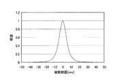
図6は、実施例1のレンズと発光ダイオードを配置し、発光ダイオードの発光面から8mmの位置に被照射面を配置したときの、計算で求めた被照射面でのX方向における照度分布を表す。図7は、同一の発光ダイオードのみ配置し、発光ダイオードの発光面から8mmの位置に被照射面を配置したときの、計算で求めた被照射面でのX方向における照度分布を表す。 FIG. 6 shows the illuminance distribution in the X direction on the irradiated surface obtained by calculation when the lens and the light emitting diode of Example 1 are arranged and the irradiated surface is arranged at a position 8 mm from the light emitting surface of the light emitting diode. To express. FIG. 7 shows the illuminance distribution in the X direction on the irradiated surface obtained by calculation when only the same light emitting diode is disposed and the irradiated surface is disposed at a position 8 mm from the light emitting surface of the light emitting diode.
図6と図7を比較すると、実施例1のレンズの効果で被照射面を広く照明できていることがわかる。 Comparing FIG. 6 and FIG. 7, it can be seen that the illuminated surface can be widely illuminated by the effect of the lens of Example 1.
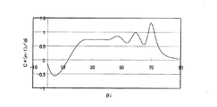
図8に、実施例1のレンズにおける微小区間の曲率Cを示す。横軸は、微小区間の中心と光軸面S上の光源位置Pとを結んだ線Liと光軸面Sとのなす角度θiである(図3参照)。曲率Cは、θi=13.77°で符号が反転し、θi=69.8°で最大となる。 FIG. 8 shows the curvature C of a minute section in the lens of Example 1. The horizontal axis is an angle θi formed by the line Li connecting the center of the minute section and the light source position P on the optical axis plane S and the optical axis plane S (see FIG. 3). The sign of the curvature C is inverted when θi = 13.77 ° and becomes maximum when θi = 69.8 °.
図9に、実施例1のレンズにおける式(5)に関連するC×(n−1)/diを示す。なお、diとは、光軸面S上の光源位置Pから、微小区間の中心までの距離、すなわち図3中の線Liの長さのことである。C×(n−1)/diは、θi=69.8°で最大となり、その値は1.33である。 FIG. 9 shows C × (n−1) / di related to Expression (5) in the lens of Example 1. In addition, di is the distance from the light source position P on the optical axis surface S to the center of the minute section, that is, the length of the line Li in FIG. C × (n−1) / di becomes maximum at θi = 69.8 °, and its value is 1.33.
図10に、実施例1のレンズにおける微小区間の曲率Cとサグ量を示す。図10では、θo=13.77°、θs=37.06°、θmc=69.8°である。 FIG. 10 shows the curvature C and the sag amount of a minute section in the lens of Example 1. In FIG. 10, θo = 13.77 °, θs = 37.06 °, and θmc = 69.8 °.
図11に、実施例1のレンズの出射面から出射される光を出射角度ごとに見たときの光度を相対光度で示す。図11では、θmp=67.7°である。従って、θmp/θmc=0.97である。 FIG. 11 shows the luminous intensity in terms of relative luminous intensity when the light emitted from the exit surface of the lens of Example 1 is viewed at each emission angle. In FIG. 11, θmp = 67.7 °. Therefore, θmp / θmc = 0.97.
《実施例2》
実施例2のレンズは、図2に対応する断面形状を有する。本実施例は、X方向幅Sxが0.65mm、Y方向幅Syが5.0mmの発光ダイオードを光源とし、その発光ダイオードの配光特性をX方向に拡大することを目的とした設計例である。実施例2の力レンズのX方向幅Lwは4.5mmである。実施例2のレンズの面データを表3に、非球面データを表4に示す。
Example 2
The lens of Example 2 has a cross-sectional shape corresponding to FIG. This embodiment is a design example for the purpose of expanding the light distribution characteristic of the light emitting diode in the X direction using a light emitting diode having an X direction width Sx of 0.65 mm and a Y direction width Sy of 5.0 mm. is there. The X direction width Lw of the force lens of Example 2 is 4.5 mm. Table 3 shows surface data of the lens of Example 2, and Table 4 shows aspherical data.
[表3]面データ
面 r d n
入射面 ∞ 1.2 1.41
出射面 1.088E-12 6.8
被照射面 ∞
[Table 3] Surface data surface r dn
Entrance plane ∞ 1.2 1.41
Outgoing surface 1.088E-12 6.8
Irradiated surface ∞
[表4]非球面データ
K=-1.0268E+01,A3=1.5843E+00,A4=-5.9328E+00,A5=1.0800E+01
A6=-1.3014E+01,A7=1.0470E+01,A8=-4.6299E+00,A9=-2.1226E-02
A10=9.6894E-01,A11=-7.9260E-02,A12=-2.3661E-01,A13=-1.8210E-03
A14=6.4025E-02,A15=1.2197E-03,A16=-1.0393E-02,A17=-1.3892E-04
A18=8.1619E-05,A19=6.2396E-04,A20=-1.5184E-04
[Table 4] Aspheric data K = -1.0268E + 01, A 3 = 1.5843E + 00, A 4 = -5.9328E + 00, A 5 = 1.0800E + 01
A 6 = -1.3014E + 01, A 7 = 1.0470E + 01, A 8 = -4.6299E + 00, A 9 = -2.1226E-02
A 10 = 9.6894E-01, A 11 = -7.9260E-02, A 12 = -2.3661E-01, A 13 = -1.8210E-03
A 14 = 6.44025E-02, A 15 = 1.2197E-03, A 16 = -1.0393E-02, A 17 = -1.3892E-04
A 18 = 8.1619E-05, A 19 = 6.2396E-04, A 20 = -1.5184E-04
図12は、実施例2のレンズと発光ダイオードを配置し、発光ダイオードの発光面から8mmの位置に被照射面を配置したときの、計算で求めた被照射面でのX方向における照度分布を表す。図13は、同一の発光ダイオードのみ配置し、発光ダイオードの発光面から8mmの位置に被照射面を配置したときの、計算で求めた被照射面でのX方向における照度分布を表す。 FIG. 12 shows the illuminance distribution in the X direction on the irradiated surface obtained by calculation when the lens and the light emitting diode of Example 2 are disposed and the irradiated surface is disposed at a position 8 mm from the light emitting surface of the light emitting diode. To express. FIG. 13 shows the illuminance distribution in the X direction on the irradiated surface obtained by calculation when only the same light emitting diode is disposed and the irradiated surface is disposed at a position 8 mm from the light emitting surface of the light emitting diode.
図12と図13を比較すると、実施例2のレンズの効果で被照射面を広く照明できていることがわかる。 Comparing FIG. 12 and FIG. 13, it can be seen that the illuminated surface can be widely illuminated by the effect of the lens of Example 2.
図14に、実施例2のレンズにおける微小区間の曲率Cを示す。横軸は、微小区間の中心と光軸面S上の光源位置Pとを結んだ線Liと光軸とのなす角度θiである(図3参照)。曲率Cは、θi=12.5°で符号が反転し、θi=67.2°で最大となる。 FIG. 14 shows the curvature C of a minute section in the lens of Example 2. The horizontal axis is an angle θi formed by a line Li connecting the center of the minute section and the light source position P on the optical axis plane S and the optical axis (see FIG. 3). The sign of the curvature C is inverted when θi = 12.5 ° and becomes maximum when θi = 67.2 °.
図15に、実施例2のレンズにおける式(4)に関連するC×(n−1)/diを示す。なお、diとは、光軸面S上の光源位置Pから、微小区間の中心までの距離、すなわち図3中の線Liの長さのことである。C×(n−1)/diは、θi=67.2°で最大となり、その値は0.995である。 FIG. 15 shows C × (n−1) / di related to Expression (4) in the lens of Example 2. In addition, di is the distance from the light source position P on the optical axis surface S to the center of the minute section, that is, the length of the line Li in FIG. C × (n−1) / di is maximum at θi = 67.2 °, and its value is 0.995.
図16に、実施例2のレンズにおける微小区間の曲率Cとサグ量を示す。図16では、θo=12.5°、θs=35.38°、θmc=67.2°である。 FIG. 16 shows the curvature C and the sag amount in a minute section in the lens of Example 2. In FIG. 16, θo = 12.5 °, θs = 35.38 °, and θmc = 67.2 °.
図17に、実施例2のレンズの出射面から出射される光を出射角度ごとに見たときの光度を相対光度で示す。図17では、θmp=62.5°である。従って、θmp/θmc=0.93である。 FIG. 17 shows the relative luminous intensity when the light emitted from the exit surface of the lens of Example 2 is viewed at each emission angle. In FIG. 17, θmp = 62.5 °. Therefore, θmp / θmc = 0.93.
各実施例のレンズにおける式(1)〜(9)の条件に対する対応値は、以下の表5のとおりである。 Corresponding values for the conditions of the expressions (1) to (9) in the lenses of the respective examples are as shown in Table 5 below.
(実施の形態2)
図18は、本発明の実施の形態2に係る発光装置1Bの斜視図である。なお、実施の形態2では、実施の形態1と同一構成部分には同一符号を付して、その説明を省略する。この点は、後述する実施の形態3でも同様である。
(Embodiment 2)
FIG. 18 is a perspective view of a
本実施形態の発光装置1Bでは、発光ダイオード3が複数(図例では3つ)設けられており、これらの発光ダイオード3はY方向に並べられた状態で基板2に実装されている。発光ダイオード3は、全て同じサイズ(例えば、幅は0.5mm、長さ5.0mm)のものであってもよい。
In the
レンズ4は、全ての発光ダイオード3に沿って延びる形状を有しており、全ての発光ダイオード3を覆っている。
The
本実施形態の発光装置1Bは、複数の発光ダイオード3を用いていることを除いては、実施の形態1と同様にして被照射面を照明する。発光装置1Bでは、複数の発光ダイオード3を用いることで、照明領域をY方向に幅広くすることができるとともに、さらに大きな光束量で被照射面を照明することができる。
The
なお、本実施形態の発光装置1Bでも、実施の形態1で説明した好ましい態様が採用されること(例えば、式(1)〜(9)の条件を満たすこと)が好ましい。この点は、後述する実施の形態3でも同様である。
In the
(実施の形態3)
図19は、本発明の実施の形態3に係る発光装置1Cの斜視図である。本実施形態の発光装置1Cは、第2実施形態の発光装置1Bと同様の構成となっているが、発光ダイオード3同士の間に、発光ダイオード3から放射される光を反射して拡散する反射拡散部25が設けられている点で異なる。
(Embodiment 3)
FIG. 19 is a perspective view of a
具体的に、反射拡散部25は、基板2に形成されている。本実施形態の各反射拡散部25は、X方向に潰れた四角錐状をなしている。各発光ダイオード3のサイズは、例えば幅0.5mm、長さ3.0mmである。各反射拡散部25の底面の大きさは、例えばX方向の短辺が0.5mm、Y方向の長辺が2.0mmである。反射拡散部25を基板2に形成するには、予め所望の形状に成形した樹脂成形品を基板2に接合すればよい。反射拡散部25は、発光ダイオード3からの光を反射して拡散することにより、擬似的な光源を形成する。
Specifically, the
発光装置1Cでは、複数の発光ダイオード3の間に反射拡散部25を設けることで、発光ダイオード3の長さを短くできるため、実施の形態2の効果をより安価に得ることができる。
In the
(変形例)
なお、前記各実施の形態では、出射面42が光軸面Sに対して面対称になっているが、出射面42は、例えば図21に示すように、光軸面Sに対して非対称になっていてもよい。
(Modification)
In each of the embodiments described above, the
また、出射面42は、必ずしも中央部が窪んでいる必要はなく、例えば断面半球状のシリンドリカル面であってもよい。ただし、出射面42が凹面部42aと凸面部42bを含んでいれば、被照射面5における光軸近傍の照度を抑えて広がりのある照度分布にすることができる。
In addition, the
さらに、実施の形態3の発光装置1Cでは、図20(a)に示すように一定の断面形状でY方向に延びるレンズ4が用いられているが、レンズ4は、図20(b)に示す変形例の発光装置1C’のように、反射拡散部25の真上では、発光ダイオード3および反射拡散部25からの光をY方向へ屈折させる形状になっていてもよい。同様に、実施の形態1,2で用いられるレンズ4も、発光ダイオード3の存しない位置では、発光ダイオード3からの光をY方向へ屈折させる形状になっていてもよい。
Furthermore, in the
<面光源>
図22は、本発明の実施の形態3に係る発光装置1Cを用いた面光源6の斜視図である。この面光源6は、平面的に配置された、複数の発光装置1Cと、これらの発光装置1Cを覆うように配置された拡散板63とを備えている。
<Surface light source>
FIG. 22 is a perspective view of the
発光装置1Cは、拡散反射板61上に、マトリクス状に配置されている。発光装置1Cは、X方向およびY方向に配列されている。拡散反射板61は、支持板62で支持されている。
The
発光装置1Cは、拡散板63の一方面(入射面)に光を照射する。すなわち、拡散板63の一方面は、図2に示した被照射面5となっている。拡散板63は、一方面に照射された光を他方面(出射面)から拡散された状態で放射する。また、拡散板63で反射された光は、拡散反射板61で反射されて再度拡散板63に照射される。
The
面光源6は、以下の式(10)を満足することが好ましい。
0.2<h/p<0.6・・・(10)
ただし、
h:発光装置1C中の発光ダイオード3の発光面3aから拡散板63の入射面までの距離
p:X方向における発光装置1Cの配列ピッチ
である。
The
0.2 <h / p <0.6 (10)
However,
h: distance from the
式(10)は、X方向の発光装置1Cの配列ピッチに対する、発光ダイオード3の発光面3aと拡散板63との距離を規定している。h/pが0.6以上になると、発光装置1Cの配列ピッチに対して拡散板63が発光装置1Cから離れすぎるため、面光源6が大型化してしまう。h/pが0.2以下になると、拡散板63上での輝度分布の均一性を確保するのが困難になり、面内での輝度ムラが大きくなる。
Expression (10) defines the distance between the
以上説明した面光源6では、発光装置1Cからの光束はX方向に広配光化されているので、発光ダイオード3の発光面3aと拡散板63の入射面との距離hが8mmという薄型を、X方向における発光装置1Cの配列ピッチpを例えば30mmで実現できる。例えば、発光装置1CをX方向に16列配置すれば37インチ(ワイド16:9)を実現できる。このとき、式(10)中のh/pは0.267である。
In the
また、発光装置1Cを用いることで、拡散板63の入射面で照度が均一化されるため、低コスト、薄型、高輝度、高画質(均一輝度分布)の面光源6を実現できる。なお、この効果は、実施の形態3の発光装置1Cの代わりに実施の形態1,2の発光装置1A,1Bを用いても、同様に得ることができる。
Further, by using the
<液晶ディスプレイ装置>
図23は、図22に示す面光源6を用いた液晶ディスプレイ装置7の斜視図である。この液晶ディスプレイ装置7は、液晶パネル71と、液晶パネル71の裏側に配置された面光源6とを備えている。
<Liquid crystal display device>
FIG. 23 is a perspective view of a liquid crystal display device 7 using the
面光源6を用いることにより、液晶パネル71を均一に照明することができるとともに、低コスト、薄型、高輝度、高画質(均一輝度分布)の液晶ディスプレイ装置7を実現できる。なお、この効果は、面光源6に、実施の形態3の発光装置1Cの代わりに実施の形態1,2の発光装置1A,1Bが用いられていても、同様に得ることができる。
By using the
1A〜1C 発光装置
3 発光ダイオード
3a 発光面
4 レンズ
42 出射面
42a 凹面部
42b 凸面部
5 被照射面
6 面光源
63 拡散板
7 液晶ディスプレイ装置
71 液晶パネル
1A to 1C
Claims (18)
前記発光ダイオードを覆うレンズであって、前記発光ダイオードに沿って延びる形状を有し、前記発光ダイオードから放射される光を前記発光ダイオードの幅方向に広げるレンズと、
を備える、発光装置。 A light emitting diode extending in a direction perpendicular to the optical axis direction;
A lens that covers the light-emitting diode, has a shape extending along the light-emitting diode, and spreads light emitted from the light-emitting diode in a width direction of the light-emitting diode;
A light emitting device comprising:
Sw/Lw<0.15・・・(1)
ただし、
Sw:前記発光ダイオードの幅
Lw:前記発光ダイオードの幅方向における前記レンズの幅
である。 The light emitting device according to any one of claims 1 to 4, which satisfies the following formula (1).
Sw / Lw <0.15 (1)
However,
Sw: width of the light emitting diode Lw: width of the lens in the width direction of the light emitting diode.
Sw/Lw<0.13・・・(1)’
ただし、
Sw:前記発光ダイオードの幅
Lw:前記発光ダイオードの幅方向における前記レンズの幅
である。 The light emitting device according to any one of claims 1 to 4, which satisfies the following formula (1) '.
Sw / Lw <0.13 (1) '
However,
Sw: width of the light emitting diode Lw: width of the lens in the width direction of the light emitting diode.
前記出射面は、前記光軸面と交差する凹面部と、前記発光ダイオードの幅方向において前記凹面部の両側に位置する凸面部とを含み、
前記レンズを前記発光ダイオードの長手方向と垂直に切断したときの幅方向断面において、前記出射面上の微小区間の曲率Cは、前記凸面部の領域内で最大となる、請求項1〜6のいずれか一項に記載の発光装置。 The lens has an emission surface that is plane-symmetric with respect to an optical axis plane that passes through the center of the light emitting diode and is perpendicular to the width direction of the light emitting diode,
The emission surface includes a concave surface portion intersecting the optical axis surface, and convex surface portions located on both sides of the concave surface portion in the width direction of the light emitting diode,
The curvature C of a minute section on the emission surface is maximized in the region of the convex portion in a cross section in the width direction when the lens is cut perpendicularly to the longitudinal direction of the light emitting diode. The light-emitting device as described in any one.
60°<θi<80°・・・(2)
ただし、
θi:前記微小区間の中心と前記光軸面上の光源位置とを結んだ線と、前記光軸面とのなす角度
である。 The light-emitting device according to claim 7, wherein the curvature C is maximized within a range defined by the following formula (2).
60 ° <θi <80 ° (2)
However,
θi: an angle formed by a line connecting the center of the minute section and the light source position on the optical axis plane and the optical axis plane.
0.88<Yr<0.98・・・(3)
ただし、
Yr:前記レンズの有効幅の半分に対する、前記光軸面から前記微小区間の中心までの距離の比
である。 The light-emitting device according to claim 7, wherein the curvature C is maximized within a range defined by the following expression (3).
0.88 <Yr <0.98 (3)
However,
Yr: The ratio of the distance from the optical axis surface to the center of the minute section with respect to half of the effective width of the lens.
0.90<θmp/θmc<1.05・・・(4)
ただし、
θmc:前記微小区間のうち曲率Cが最大となる微小区間の中心と前記光軸面上の光源位置とを結んだ線と、前記光軸面とのなす角度
θmp:前記出射面から出射される光を前記光軸面に対する角度である出射角度ごとに見たときの最大の光度となる出射角度
である。 The light emitting device according to any one of claims 7 to 9, wherein the emission surface satisfies the following expression (4).
0.90 <θmp / θmc <1.05 (4)
However,
θmc: an angle formed by a line connecting the center of the minute section having the maximum curvature C in the minute section and the light source position on the optical axis surface and the optical axis surface θmp: emitted from the emission surface The emission angle is the maximum luminous intensity when light is viewed at each emission angle that is an angle with respect to the optical axis plane.
0.9<Cm×(n−1)/d<1.5・・・(5)
ただし、
Cm:前記曲率Cの最大値
n:前記レンズの屈折率
d:前記光軸面上の光源位置から、前記微小区間のうち曲率Cが最大となる微小区間の中心までの距離
である。 The light emitting device according to any one of claims 7 to 10, wherein the emission surface satisfies the following expression (5).
0.9 <Cm × (n−1) / d <1.5 (5)
However,
Cm: Maximum value of the curvature C n: Refractive index of the lens d: Distance from the light source position on the optical axis surface to the center of the minute section where the curvature C is maximum among the minute sections.
前記出射面は、以下の式(6)および式(7)を満足する、請求項7〜11のいずれか一項に記載の発光装置。
5°<θo<20°・・・(6)
25°<θs<45°・・・(7)
ただし、
θo:前記出射面上の曲率Cが負から正に変わる位置と前記光軸面上の光源位置とを結んだ線と、前記光軸面とのなす角度
θs:前記出射面上のサグ量が最大となる位置と前記光軸面上の光源位置とを結んだ線と、前記光軸面とのなす角度
である。 The sign of the curvature C is positive when the center of curvature is closer to the light emitting diode than the exit surface, and negative when the center of curvature is on the opposite side, and the sag amount of the exit surface intersects the optical axis surface. When standardized at the position where
The light emitting device according to any one of claims 7 to 11, wherein the emission surface satisfies the following expressions (6) and (7).
5 ° <θo <20 ° (6)
25 ° <θs <45 ° (7)
However,
θo: an angle formed by a line connecting a position where the curvature C on the exit surface changes from negative to positive and a light source position on the optical axis surface and the optical axis surface θs: a sag amount on the output surface It is an angle formed by a line connecting the maximum position and the light source position on the optical axis plane and the optical axis plane.
1.40<n<1.52・・・(8)
ただし、
n:前記レンズの屈折率
である。 The light-emitting device according to claim 1, wherein the light-emitting device satisfies the following formula (8).
1.40 <n <1.52 (8)
However,
n: Refractive index of the lens.
Sw/t<0.6・・・(9)
ただし、
Sw:前記発光ダイオードの幅
t:前記光軸面上での前記レンズの厚み
である。 The light-emitting device according to claim 1, wherein the light-emitting device satisfies the following formula (9).
Sw / t <0.6 (9)
However,
Sw: width of the light emitting diode t: thickness of the lens on the optical axis surface.
前記複数の発光装置のそれぞれは、請求項1〜15のいずれか一項に記載の発光装置であり、前記複数の発光装置は、前記発光ダイオードの長手方向および幅方向に配列されている、面光源。 A plurality of light emitting devices arranged in a plane, and a diffusion plate arranged so as to cover the plurality of light emitting devices and radiating light irradiated on one surface from the plurality of light emitting devices in a state of diffusing from the other surface; A surface light source comprising:
Each of the plurality of light emitting devices is the light emitting device according to any one of claims 1 to 15, wherein the plurality of light emitting devices are arranged in a longitudinal direction and a width direction of the light emitting diode. light source.
0.2<h/p<0.6・・・(10)
ただし、
h:前記発光装置中の発光ダイオードの発光面から前記拡散板の前記一方面までの距離
p:前記発光ダイオードの幅方向における前記発光装置の配列ピッチ
である。 The surface light source of Claim 16 which satisfies the following formula | equation (10).
0.2 <h / p <0.6 (10)
However,
h: distance from the light emitting surface of the light emitting diode in the light emitting device to the one surface of the diffusion plate p: the arrangement pitch of the light emitting devices in the width direction of the light emitting diode.
Priority Applications (1)
| Application Number | Priority Date | Filing Date | Title |
|---|---|---|---|
| JP2009159753A JP2011014831A (en) | 2009-07-06 | 2009-07-06 | Light emitting device, surface light source, and liquid crystal display device |
Applications Claiming Priority (1)
| Application Number | Priority Date | Filing Date | Title |
|---|---|---|---|
| JP2009159753A JP2011014831A (en) | 2009-07-06 | 2009-07-06 | Light emitting device, surface light source, and liquid crystal display device |
Publications (1)
| Publication Number | Publication Date |
|---|---|
| JP2011014831A true JP2011014831A (en) | 2011-01-20 |
Family
ID=43593416
Family Applications (1)
| Application Number | Title | Priority Date | Filing Date |
|---|---|---|---|
| JP2009159753A Pending JP2011014831A (en) | 2009-07-06 | 2009-07-06 | Light emitting device, surface light source, and liquid crystal display device |
Country Status (1)
| Country | Link |
|---|---|
| JP (1) | JP2011014831A (en) |
Cited By (14)
| Publication number | Priority date | Publication date | Assignee | Title |
|---|---|---|---|---|
| CN102853289A (en) * | 2012-03-19 | 2013-01-02 | 中微光电子(潍坊)有限公司 | Light-emitting diode (LED) optical system |
| KR20130073328A (en) * | 2011-12-23 | 2013-07-03 | 서울반도체 주식회사 | Light emitting module and lens |
| WO2013115200A1 (en) * | 2012-02-01 | 2013-08-08 | シャープ株式会社 | Illumination apparatus, and liquid crystal display apparatus and television receiver apparatus provided with same |
| JP2013152811A (en) * | 2012-01-24 | 2013-08-08 | Sharp Corp | Lighting device, display device, and television receiving apparatus |
| US9169980B2 (en) | 2013-03-27 | 2015-10-27 | Koha Co., Ltd. | Lighting device and display device |
| KR20150130692A (en) * | 2014-05-14 | 2015-11-24 | 엘지이노텍 주식회사 | Light emitting device module |
| KR101850981B1 (en) * | 2011-12-23 | 2018-04-20 | 서울반도체 주식회사 | Light emitting module and lens |
| JP2018073490A (en) * | 2016-10-25 | 2018-05-10 | 三菱電機株式会社 | Surface light source device and display device |
| KR101861233B1 (en) * | 2012-03-26 | 2018-07-02 | 서울반도체 주식회사 | Light emitting unit array and light diffusing lens adjustable for the smae |
| US10047930B2 (en) | 2011-12-02 | 2018-08-14 | Seoul Semiconductor Co., Ltd. | Light emitting module and lens |
| US10060579B2 (en) | 2011-12-02 | 2018-08-28 | Seoul Semiconductor Co., Ltd. | Light emitting module and lens |
| JP2020107595A (en) * | 2018-12-26 | 2020-07-09 | エクセレンス オプトエレクトロニクス インコーポレイテッド | Vehicular led linear illuminating module |
| CN112859433A (en) * | 2019-11-12 | 2021-05-28 | 恩普乐股份有限公司 | Surface light source device and display device |
| JP2024513908A (en) * | 2021-04-08 | 2024-03-27 | シグニファイ ホールディング ビー ヴィ | optical detector |
-
2009
- 2009-07-06 JP JP2009159753A patent/JP2011014831A/en active Pending
Cited By (19)
| Publication number | Priority date | Publication date | Assignee | Title |
|---|---|---|---|---|
| US10047930B2 (en) | 2011-12-02 | 2018-08-14 | Seoul Semiconductor Co., Ltd. | Light emitting module and lens |
| US10060579B2 (en) | 2011-12-02 | 2018-08-28 | Seoul Semiconductor Co., Ltd. | Light emitting module and lens |
| KR101850981B1 (en) * | 2011-12-23 | 2018-04-20 | 서울반도체 주식회사 | Light emitting module and lens |
| KR20130073328A (en) * | 2011-12-23 | 2013-07-03 | 서울반도체 주식회사 | Light emitting module and lens |
| KR101887624B1 (en) * | 2011-12-23 | 2018-08-13 | 서울반도체 주식회사 | Light emitting module and lens |
| JP2013152811A (en) * | 2012-01-24 | 2013-08-08 | Sharp Corp | Lighting device, display device, and television receiving apparatus |
| US9541259B2 (en) | 2012-02-01 | 2017-01-10 | Sharp Kabushiki Kaisha | Illumination apparatus, and liquid crystal display apparatus and television receiver apparatus provided with same |
| WO2013115200A1 (en) * | 2012-02-01 | 2013-08-08 | シャープ株式会社 | Illumination apparatus, and liquid crystal display apparatus and television receiver apparatus provided with same |
| CN102853289A (en) * | 2012-03-19 | 2013-01-02 | 中微光电子(潍坊)有限公司 | Light-emitting diode (LED) optical system |
| CN102853289B (en) * | 2012-03-19 | 2014-08-13 | 中微光电子(潍坊)有限公司 | Light-emitting diode (LED) optical system |
| KR101861233B1 (en) * | 2012-03-26 | 2018-07-02 | 서울반도체 주식회사 | Light emitting unit array and light diffusing lens adjustable for the smae |
| US9169980B2 (en) | 2013-03-27 | 2015-10-27 | Koha Co., Ltd. | Lighting device and display device |
| KR20150130692A (en) * | 2014-05-14 | 2015-11-24 | 엘지이노텍 주식회사 | Light emitting device module |
| KR102173118B1 (en) * | 2014-05-14 | 2020-11-03 | 엘지이노텍 주식회사 | Light emitting device module |
| JP2018073490A (en) * | 2016-10-25 | 2018-05-10 | 三菱電機株式会社 | Surface light source device and display device |
| JP2020107595A (en) * | 2018-12-26 | 2020-07-09 | エクセレンス オプトエレクトロニクス インコーポレイテッド | Vehicular led linear illuminating module |
| CN112859433A (en) * | 2019-11-12 | 2021-05-28 | 恩普乐股份有限公司 | Surface light source device and display device |
| CN112859433B (en) * | 2019-11-12 | 2023-07-18 | 恩普乐股份有限公司 | Surface light source device and display device |
| JP2024513908A (en) * | 2021-04-08 | 2024-03-27 | シグニファイ ホールディング ビー ヴィ | optical detector |
Similar Documents
| Publication | Publication Date | Title |
|---|---|---|
| JP4489843B2 (en) | LIGHTING LENS AND LIGHT EMITTING DEVICE, SURFACE LIGHT SOURCE, AND LIQUID CRYSTAL DISPLAY DEVICE USING THE SAME | |
| JP5518881B2 (en) | Light emitting device, surface light source, and liquid crystal display device | |
| JP5081988B2 (en) | Lighting lens, light emitting device, surface light source, and liquid crystal display device | |
| JP4546579B1 (en) | Lighting lens, light emitting device, surface light source, and liquid crystal display device | |
| US8743315B2 (en) | Surface light source device, liquid crystal display device, and lens | |
| JP5380182B2 (en) | Light emitting device, surface light source, and liquid crystal display device | |
| JP5342939B2 (en) | Lighting lens, light emitting device, surface light source, and liquid crystal display device | |
| US20130114022A1 (en) | Light emitting device, surface light source, liquid crystal display device, and lens | |
| JPWO2012164790A1 (en) | Surface light source and liquid crystal display device | |
| JP5118617B2 (en) | Lighting lens, light emitting device, surface light source, and liquid crystal display device | |
| JP2011014434A5 (en) | ||
| US10352530B2 (en) | Lens, light emitting apparatus including the lens, and backlight unit including the apparatus | |
| JP2011009052A (en) | Surface light source, and liquid crystal display device | |
| JP2010186142A (en) | Lens for illumination, light emitter, surface light source, and liquid crystal display device | |
| KR20140060625A (en) | Light emitting device and lighting device having the same | |
| TWI503581B (en) | Lens, light source device and direct type light source module | |
| JP5849192B2 (en) | Surface light source and liquid crystal display device | |
| JP5342938B2 (en) | Lighting lens, light emitting device, surface light source, and liquid crystal display device | |
| JP2010146986A (en) | Lens for illumination, light-emitting device, plane light source, and liquid crystal display | |
| KR101355815B1 (en) | Light emitting device and lighting device having the same | |
| JP5342940B2 (en) | Lighting lens, light emitting device, surface light source, and liquid crystal display device | |
| KR101907064B1 (en) | Optical lens | |
| JP2011003462A (en) | Illuminating lens, lighting device, surface light source, and liquid crystal display apparatus | |
| JP2011228226A (en) | Lens for lighting, light-emitting device, plane light source, and liquid crystal display | |
| WO2018135559A1 (en) | Luminous flux control member, light-emitting device, planar light source device, and display device |