JP7698643B2 - 光通信モジュール基板 - Google Patents
光通信モジュール基板 Download PDFInfo
- Publication number
- JP7698643B2 JP7698643B2 JP2022531964A JP2022531964A JP7698643B2 JP 7698643 B2 JP7698643 B2 JP 7698643B2 JP 2022531964 A JP2022531964 A JP 2022531964A JP 2022531964 A JP2022531964 A JP 2022531964A JP 7698643 B2 JP7698643 B2 JP 7698643B2
- Authority
- JP
- Japan
- Prior art keywords
- optical
- wiring
- electrical
- board
- substrate
- Prior art date
- Legal status (The legal status is an assumption and is not a legal conclusion. Google has not performed a legal analysis and makes no representation as to the accuracy of the status listed.)
- Active
Links
Images


Classifications
-
- H—ELECTRICITY
- H05—ELECTRIC TECHNIQUES NOT OTHERWISE PROVIDED FOR
- H05K—PRINTED CIRCUITS; CASINGS OR CONSTRUCTIONAL DETAILS OF ELECTRIC APPARATUS; MANUFACTURE OF ASSEMBLAGES OF ELECTRICAL COMPONENTS
- H05K1/00—Printed circuits
- H05K1/02—Details
- H05K1/11—Printed elements for providing electric connections to or between printed circuits
- H05K1/117—Pads along the edge of rigid circuit boards, e.g. for pluggable connectors
-
- G—PHYSICS
- G02—OPTICS
- G02B—OPTICAL ELEMENTS, SYSTEMS OR APPARATUS
- G02B6/00—Light guides; Structural details of arrangements comprising light guides and other optical elements, e.g. couplings
- G02B6/10—Light guides; Structural details of arrangements comprising light guides and other optical elements, e.g. couplings of the optical waveguide type
- G02B6/12—Light guides; Structural details of arrangements comprising light guides and other optical elements, e.g. couplings of the optical waveguide type of the integrated circuit kind
-
- G—PHYSICS
- G02—OPTICS
- G02B—OPTICAL ELEMENTS, SYSTEMS OR APPARATUS
- G02B6/00—Light guides; Structural details of arrangements comprising light guides and other optical elements, e.g. couplings
- G02B6/24—Coupling light guides
- G02B6/42—Coupling light guides with opto-electronic elements
- G02B6/4201—Packages, e.g. shape, construction, internal or external details
- G02B6/4204—Packages, e.g. shape, construction, internal or external details the coupling comprising intermediate optical elements, e.g. lenses, holograms
- G02B6/4214—Packages, e.g. shape, construction, internal or external details the coupling comprising intermediate optical elements, e.g. lenses, holograms the intermediate optical element having redirecting reflective means, e.g. mirrors, prisms for deflecting the radiation from horizontal to down- or upward direction toward a device
-
- G—PHYSICS
- G02—OPTICS
- G02B—OPTICAL ELEMENTS, SYSTEMS OR APPARATUS
- G02B6/00—Light guides; Structural details of arrangements comprising light guides and other optical elements, e.g. couplings
- G02B6/24—Coupling light guides
- G02B6/42—Coupling light guides with opto-electronic elements
- G02B6/4201—Packages, e.g. shape, construction, internal or external details
- G02B6/4274—Electrical aspects
- G02B6/428—Electrical aspects containing printed circuit boards [PCB]
-
- H—ELECTRICITY
- H05—ELECTRIC TECHNIQUES NOT OTHERWISE PROVIDED FOR
- H05K—PRINTED CIRCUITS; CASINGS OR CONSTRUCTIONAL DETAILS OF ELECTRIC APPARATUS; MANUFACTURE OF ASSEMBLAGES OF ELECTRICAL COMPONENTS
- H05K1/00—Printed circuits
- H05K1/02—Details
- H05K1/0213—Electrical arrangements not otherwise provided for
- H05K1/0237—High frequency adaptations
- H05K1/0245—Lay-out of balanced signal pairs, e.g. differential lines or twisted lines
-
- H—ELECTRICITY
- H05—ELECTRIC TECHNIQUES NOT OTHERWISE PROVIDED FOR
- H05K—PRINTED CIRCUITS; CASINGS OR CONSTRUCTIONAL DETAILS OF ELECTRIC APPARATUS; MANUFACTURE OF ASSEMBLAGES OF ELECTRICAL COMPONENTS
- H05K1/00—Printed circuits
- H05K1/02—Details
- H05K1/0271—Arrangements for reducing stress or warp in rigid printed circuit boards, e.g. caused by loads, vibrations or differences in thermal expansion
-
- H—ELECTRICITY
- H05—ELECTRIC TECHNIQUES NOT OTHERWISE PROVIDED FOR
- H05K—PRINTED CIRCUITS; CASINGS OR CONSTRUCTIONAL DETAILS OF ELECTRIC APPARATUS; MANUFACTURE OF ASSEMBLAGES OF ELECTRICAL COMPONENTS
- H05K1/00—Printed circuits
- H05K1/02—Details
- H05K1/14—Structural association of two or more printed circuits
- H05K1/144—Stacked arrangements of planar printed circuit boards
-
- H—ELECTRICITY
- H05—ELECTRIC TECHNIQUES NOT OTHERWISE PROVIDED FOR
- H05K—PRINTED CIRCUITS; CASINGS OR CONSTRUCTIONAL DETAILS OF ELECTRIC APPARATUS; MANUFACTURE OF ASSEMBLAGES OF ELECTRICAL COMPONENTS
- H05K2201/00—Indexing scheme relating to printed circuits covered by H05K1/00
- H05K2201/04—Assemblies of printed circuits
- H05K2201/041—Stacked PCBs, i.e. having neither an empty space nor mounted components in between
-
- H—ELECTRICITY
- H05—ELECTRIC TECHNIQUES NOT OTHERWISE PROVIDED FOR
- H05K—PRINTED CIRCUITS; CASINGS OR CONSTRUCTIONAL DETAILS OF ELECTRIC APPARATUS; MANUFACTURE OF ASSEMBLAGES OF ELECTRICAL COMPONENTS
- H05K2201/00—Indexing scheme relating to printed circuits covered by H05K1/00
- H05K2201/09—Shape and layout
- H05K2201/09209—Shape and layout details of conductors
- H05K2201/09218—Conductive traces
- H05K2201/09227—Layout details of a plurality of traces, e.g. escape layout for Ball Grid Array [BGA] mounting
-
- H—ELECTRICITY
- H05—ELECTRIC TECHNIQUES NOT OTHERWISE PROVIDED FOR
- H05K—PRINTED CIRCUITS; CASINGS OR CONSTRUCTIONAL DETAILS OF ELECTRIC APPARATUS; MANUFACTURE OF ASSEMBLAGES OF ELECTRICAL COMPONENTS
- H05K2201/00—Indexing scheme relating to printed circuits covered by H05K1/00
- H05K2201/10—Details of components or other objects attached to or integrated in a printed circuit board
- H05K2201/10007—Types of components
- H05K2201/10121—Optical component, e.g. opto-electronic component
-
- H—ELECTRICITY
- H05—ELECTRIC TECHNIQUES NOT OTHERWISE PROVIDED FOR
- H05K—PRINTED CIRCUITS; CASINGS OR CONSTRUCTIONAL DETAILS OF ELECTRIC APPARATUS; MANUFACTURE OF ASSEMBLAGES OF ELECTRICAL COMPONENTS
- H05K2201/00—Indexing scheme relating to printed circuits covered by H05K1/00
- H05K2201/10—Details of components or other objects attached to or integrated in a printed circuit board
- H05K2201/10227—Other objects, e.g. metallic pieces
- H05K2201/1034—Edge terminals, i.e. separate pieces of metal attached to the edge of the printed circuit board [PCB]
Landscapes
- Physics & Mathematics (AREA)
- Engineering & Computer Science (AREA)
- Microelectronics & Electronic Packaging (AREA)
- General Physics & Mathematics (AREA)
- Optics & Photonics (AREA)
- Structure Of Printed Boards (AREA)
- Optical Integrated Circuits (AREA)
- Semiconductor Lasers (AREA)
Description
[1]配線基板と光電気混載基板とを接続してなる光通信モジュール基板であって、
上記配線基板が、電気配線Xとその接続用端子を備え、
上記光電気混載基板が、絶縁層と、上記絶縁層の第1の面側に設けられ、光素子実装用のパッドと電気配線Yとその接続用端子を有する電気回路部と、上記絶縁層の第2の面側に設けられた金属補強層と、同じく上記絶縁層の第2の面側に、その一部が上記金属補強層と重なる配置で設けられた光導波路とを備え、
上記配線基板の接続用端子と上記光電気混載基板の接続用端子とが、電気的な接続点になっており、
上記光電気混載基板の金属補強層が、上記絶縁層を挟んで反対側に設けられる上記電気配線Yの接続用端子に対峙する部分において、端子ごとにその端子を囲うように除去されて、枠状除去部が形成されている光通信モジュール基板。
[2]上記金属補強層の、上記枠状除去部に囲われた部分が、それぞれ、上記電気配線Yの接続用端子と導通されている上記[1]記載の光通信モジュール基板。
[3]上記金属補強層のうち、上記絶縁層を挟んで反対側に設けられる電気配線Yに対峙する部分が、電気配線Yに沿って帯状に除去されている上記[1]または[2]記載の光通信モジュール基板。
[4]上記配線基板の接続用端子と上記光電気混載基板の接続用端子とが、互いに重なり合うよう配置され、重なり合う接続用端子同士が、互いに直接もしくは導電部材を介して電気的に接続されている上記[1]~[3]のいずれかに記載の光通信モジュール基板。[5]上記配線基板の接続用端子と上記光電気混載基板の接続用端子とが、上記配線基板と光電気混載基板の間に配設された電気コネクタを介して電気的に接続されている上記[1]~[3]のいずれかに記載の光通信モジュール基板。
つぎに、上記光電気混載基板30を得る工程の一例を、具体的な材料を例示しつつ簡単に説明する。
(1)電気回路部Eの形成
まず、図4に示すように、金属補強層37となる金属板100を用意し、その表面に、ポリイミド等の感光性絶縁樹脂を塗布して、絶縁層31となる絶縁樹脂層101を形成する。
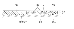
つぎに、上記絶縁層31を挟んで電気回路部Eとは反対側の金属補強層37に、エッチング処理(ドライフィルムレジストラミネート、露光、現像、エッチング、ドライフィルムレジスト剥離等)を施して、不要な部分を除去して、所定のパターン形状にする。これにより、図6に示すように、光素子32(図1を参照)との光結合用の貫通孔50や、接続用端子35に対峙する部分における枠状除去部60等が形成される。
つぎに、上記電気回路部Eと金属補強層37を備えた絶縁層31を上下逆にして、金属補強層37を上に向ける。そして、上記絶縁層31の、金属補強層37が形成された側の面に、公知の方法によってアンダークラッド層40とコア41とオーバークラッド層42とを、必要に応じて各層を所定パターンにパターニングした状態で、積層形成することにより、光導波路Wを得ることができる。
てもよい。
このようにして得られた光電気混載基板30と、前記配線基板20を、図1に示すように、互いの接続用端子35、22が重なる配置とし、互いの接合部をハンダバンプ等により、電気的に接続する。そして、上記配線基板20と光電気混載基板30を安定的に組み付ける。これによって、目的とする光通信モジュール基板を得ることができる。
まず、図10(a)に示すような幅10mm×長さ60mmの帯状の配線基板を作製した。基板は、絶縁層120を挟んで裏面に金属補強層121が形成され、表面に差動伝送用の2本一対の電気配線Y1が形成された構成になっており、上記電気配線Y1の両端部には、接続用端子122が設けられている。
絶縁層120:ポリイミド、厚み10μm
金属補強層121:ステンレス、厚み20μm
電気配線Y1:銅、厚み6μm(接続用端子122は金メッキ付)
そして、上記配線基板に、図10(b)に示すように、上記接続用端子122に対峙する金属補強層121の部分において、各端子122を個別に囲う枠状除去部123と電気配線Y1に沿う帯状除去部124とを形成することにより、実施例サンプル1とした。なお、絶縁層120の、上記接続用端子122に対応する位置に貫通孔を形成しておき、電気配線Y1の形成材料である銅を、この貫通孔内に充填させて、金属補強層121の、枠状除去部123によって独立した小片部分を導通した(図3を参照)。
また、図10(c)に示すように、上記配線基板の金属補強層121に、上記実施例サンプルのような枠状除去部123は形成せず、電気配線Y1に沿う帯状除去部124のみを形成することにより、比較例サンプル1とした。
各サンプルに対して、サンプリング・オシロスコープDSA8200とTDRモジュール80E04からなる装置(テクトロニクス社製)を用いたタイム・ドメイン・リフレクトメトリー(TDR)法にて、差動インピーダンス(Ω)を測定した。
上記TDR法は、高速な立ち上がり時間をもつパルス波をサンプルに入力し、インピーダンス不整合部で生じる反射現象を利用してインピーダンスを計測するものである。これにより、接続部におけるインピーダンス整合を評価することができる。
各サンプルに対して、4ポート構成のベクトル・ネットワークアナライザN5232A装置(キーサイト・テクノロジ―社製)を用いて、差動信号入力時の挿入損失(Sdd21)を測定した。
上記挿入損失は、サンプルへの入力信号エネルギーに対する透過信号エネルギーの比を、dB表示したものである。これにより、高周波信号品質を評価することができる。
[実施例サンプル2]
前記の記載に従い、図9に示す構成の光通信モジュール基板(実施例サンプル2)を作製した。各層の構造等は、一般的な光通信モジュール基板の構造に準じており、その詳細を省略する。なお、この実施例サンプル2において、光電気混載基板30側の、高速差動信号用の接続用端子35は一列8個であり、8個の枠状除去部60が形成されている(図2を参照)。そして、上記接続用端子35を、配線基板20側の接続端子22に接続するための電気コネクタ70として、ZIFコネクタ(FH43B-21S-0.2SHW、ヒロセ電機社製)を用いた。
上記枠状除去部60を形成しない以外は、実施例サンプル2と同様にして、光通信モジュール基板(比較例サンプル2)を作製した。

31 絶縁層
35 接続用端子
37 金属補強層
60 枠状除去部
Claims (5)
- 配線基板と光電気混載基板とを接続してなる光通信モジュール基板であって、
上記配線基板が、電気配線Xとその接続用端子を備え、
上記光電気混載基板が、絶縁層と、上記絶縁層の第1の面側に設けられ、光素子実装用のパッドと電気配線Yとその接続用端子を有する電気回路部と、上記絶縁層の第2の面側に設けられた金属補強層と、同じく上記絶縁層の第2の面側に、その一部が上記金属補強層と重なる配置で設けられた光導波路とを備え、
上記配線基板の接続用端子と上記光電気混載基板の接続用端子とが、電気的な接続点になっており、
上記光電気混載基板の金属補強層が、上記絶縁層を挟んで反対側に設けられる上記電気配線Yの接続用端子に対峙する部分において、端子ごとにその端子を囲うように除去されて、枠状除去部が形成され、枠状除去部の内側が周囲から独立した小片となっている光通信モジュール基板。 - 上記金属補強層の、上記枠状除去部に囲われた部分が、それぞれ、上記電気配線Yの接続用端子と導通されている請求項1記載の光通信モジュール基板。
- 上記金属補強層のうち、上記絶縁層を挟んで反対側に設けられる電気配線Yに対峙する部分が、電気配線Yに沿って帯状に除去されている請求項1または2記載の光通信モジュール基板。
- 上記配線基板の接続用端子と上記光電気混載基板の接続用端子とが、互いに重なり合うよう配置され、重なり合う接続用端子同士が、互いに直接もしくは導電部材を介して電気的に接続されている請求項1~3のいずれか一項に記載の光通信モジュール基板。
- 上記配線基板の接続用端子と上記光電気混載基板の接続用端子とが、上記配線基板と光 電気混載基板の間に配設された電気コネクタを介して電気的に接続されている請求項1~3のいずれか一項に記載の光通信モジュール基板。
Applications Claiming Priority (3)
| Application Number | Priority Date | Filing Date | Title |
|---|---|---|---|
| JP2020107046 | 2020-06-22 | ||
| JP2020107046 | 2020-06-22 | ||
| PCT/JP2021/023349 WO2021261428A1 (ja) | 2020-06-22 | 2021-06-21 | 光通信モジュール基板 |
Publications (2)
| Publication Number | Publication Date |
|---|---|
| JPWO2021261428A1 JPWO2021261428A1 (ja) | 2021-12-30 |
| JP7698643B2 true JP7698643B2 (ja) | 2025-06-25 |
Family
ID=79281403
Family Applications (1)
| Application Number | Title | Priority Date | Filing Date |
|---|---|---|---|
| JP2022531964A Active JP7698643B2 (ja) | 2020-06-22 | 2021-06-21 | 光通信モジュール基板 |
Country Status (5)
| Country | Link |
|---|---|
| US (1) | US12369251B2 (ja) |
| JP (1) | JP7698643B2 (ja) |
| CN (1) | CN115698792A (ja) |
| TW (1) | TWI884282B (ja) |
| WO (1) | WO2021261428A1 (ja) |
Families Citing this family (1)
| Publication number | Priority date | Publication date | Assignee | Title |
|---|---|---|---|---|
| WO2021261428A1 (ja) * | 2020-06-22 | 2021-12-30 | 日東電工株式会社 | 光通信モジュール基板 |
Citations (6)
| Publication number | Priority date | Publication date | Assignee | Title |
|---|---|---|---|---|
| US20020012885A1 (en) | 2000-05-09 | 2002-01-31 | Steinberg Dan A. | Multi-level optical structure and method of manufacture |
| JP2004363205A (ja) | 2003-06-03 | 2004-12-24 | Nitto Denko Corp | 配線回路基板 |
| JP2007123740A (ja) | 2005-10-31 | 2007-05-17 | Sony Corp | フレキシブル基板、光送受信モジュール及び光送受信装置 |
| JP2014082455A (ja) | 2012-09-27 | 2014-05-08 | Mitsubishi Electric Corp | フレキシブル基板及び基板接続構造 |
| JP2016085314A (ja) | 2014-10-24 | 2016-05-19 | 日東電工株式会社 | 光電気混載基板およびその製法 |
| JP2016540388A (ja) | 2013-09-17 | 2016-12-22 | タイコ エレクトロニクス スベンスカ ホールディングス アーベー | 回路接続領域付近にインピーダンス補償部を有するe/oエンジンのための相互接続構造体 |
Family Cites Families (14)
| Publication number | Priority date | Publication date | Assignee | Title |
|---|---|---|---|---|
| JP5125632B2 (ja) | 2008-03-10 | 2013-01-23 | セイコーエプソン株式会社 | 実装構造体および電気光学装置 |
| JP5604840B2 (ja) * | 2009-09-29 | 2014-10-15 | 大日本印刷株式会社 | サスペンション用基板、サスペンション、ヘッド付サスペンションおよびハードディスクドライブ |
| PH12012500652A1 (en) * | 2009-09-30 | 2012-10-22 | Sumitomo Bakelite Co | Conductive connecting material, method for connecting terminals and method for producing connection terminal |
| US9720171B2 (en) * | 2012-06-19 | 2017-08-01 | Sumitomo Bakelite Co., Ltd. | Optical waveguide, optical interconnection component, optical module, opto-electric hybrid board, and electronic device |
| JP6202662B2 (ja) * | 2012-11-27 | 2017-09-27 | 日東電工株式会社 | 光電気混載基板およびその製法 |
| JP6319762B2 (ja) * | 2013-10-31 | 2018-05-09 | 日東電工株式会社 | 光電気混載基板およびその製法 |
| US9651751B1 (en) * | 2016-03-10 | 2017-05-16 | Inphi Corporation | Compact optical transceiver by hybrid multichip integration |
| JP2018010030A (ja) * | 2016-07-11 | 2018-01-18 | 富士通コンポーネント株式会社 | 光モジュール |
| CN109804720A (zh) * | 2016-12-28 | 2019-05-24 | 株式会社藤仓 | 布线体组件、布线基板以及接触式传感器 |
| TWI670999B (zh) * | 2017-11-22 | 2019-09-01 | 日商阿爾卑斯阿爾派股份有限公司 | 輸入裝置 |
| JP7489756B2 (ja) * | 2018-07-25 | 2024-05-24 | 日東電工株式会社 | 光学素子装置およびその製造方法 |
| WO2021261428A1 (ja) * | 2020-06-22 | 2021-12-30 | 日東電工株式会社 | 光通信モジュール基板 |
| WO2022024756A1 (ja) * | 2020-07-29 | 2022-02-03 | 日東電工株式会社 | 光電気混載基板 |
| US12392970B2 (en) * | 2021-09-22 | 2025-08-19 | Intel Corporation | Photonic integrated circuit packaging architectures |
-
2021
- 2021-06-21 WO PCT/JP2021/023349 patent/WO2021261428A1/ja not_active Ceased
- 2021-06-21 JP JP2022531964A patent/JP7698643B2/ja active Active
- 2021-06-21 CN CN202180039782.8A patent/CN115698792A/zh active Pending
- 2021-06-21 US US18/009,063 patent/US12369251B2/en active Active
- 2021-06-21 TW TW110122524A patent/TWI884282B/zh active
Patent Citations (6)
| Publication number | Priority date | Publication date | Assignee | Title |
|---|---|---|---|---|
| US20020012885A1 (en) | 2000-05-09 | 2002-01-31 | Steinberg Dan A. | Multi-level optical structure and method of manufacture |
| JP2004363205A (ja) | 2003-06-03 | 2004-12-24 | Nitto Denko Corp | 配線回路基板 |
| JP2007123740A (ja) | 2005-10-31 | 2007-05-17 | Sony Corp | フレキシブル基板、光送受信モジュール及び光送受信装置 |
| JP2014082455A (ja) | 2012-09-27 | 2014-05-08 | Mitsubishi Electric Corp | フレキシブル基板及び基板接続構造 |
| JP2016540388A (ja) | 2013-09-17 | 2016-12-22 | タイコ エレクトロニクス スベンスカ ホールディングス アーベー | 回路接続領域付近にインピーダンス補償部を有するe/oエンジンのための相互接続構造体 |
| JP2016085314A (ja) | 2014-10-24 | 2016-05-19 | 日東電工株式会社 | 光電気混載基板およびその製法 |
Also Published As
| Publication number | Publication date |
|---|---|
| TW202220506A (zh) | 2022-05-16 |
| JPWO2021261428A1 (ja) | 2021-12-30 |
| US20230254973A1 (en) | 2023-08-10 |
| US12369251B2 (en) | 2025-07-22 |
| TWI884282B (zh) | 2025-05-21 |
| WO2021261428A1 (ja) | 2021-12-30 |
| CN115698792A (zh) | 2023-02-03 |
Similar Documents
| Publication | Publication Date | Title |
|---|---|---|
| US8044746B2 (en) | Flexible interconnect cable with first and second signal traces disposed between first and second ground traces so as to provide different line width and line spacing configurations | |
| US7121859B2 (en) | Flexible cable interconnect assembly | |
| US7990165B2 (en) | Contact probe and method of making the same | |
| KR101232691B1 (ko) | 배선기판 및 프로브 카드 | |
| US12366715B2 (en) | Opto-electric hybrid board | |
| JP2014013196A (ja) | 高周波プローブ | |
| JP5609451B2 (ja) | コネクタ、光伝送装置およびコネクタ接続方法 | |
| JP7698643B2 (ja) | 光通信モジュール基板 | |
| US8585432B2 (en) | Connector and optical transmission apparatus | |
| JP5950764B2 (ja) | プリント配線板 | |
| JP4427645B2 (ja) | コンタクトプローブ、そのコンタクトプローブに用いる測定用パッド、及びそのコンタクトプローブの作製方法 | |
| JP2013065657A (ja) | プリント配線基板およびプリント配線基板の配線方法 | |
| WO2010061582A1 (ja) | 回路モジュールの基板及びその製造方法 | |
| US20230280554A1 (en) | Opto-electric hybrid board, optical communication module using same, and optical element inspection method | |
| US20060166525A1 (en) | Evaluation board and cable assembly evaluation method | |
| CN222953523U (zh) | 光模块用eml基板、eml coc组件及光模块 | |
| JP7255702B2 (ja) | 高周波線路接続構造 | |
| JP7242613B2 (ja) | 基板間接続構造および基板間接続方法 | |
| JP4418883B2 (ja) | 集積回路チップの試験検査装置、集積回路チップの試験検査用コンタクト構造体及びメッシュコンタクト | |
| JP5235000B2 (ja) | フレキシブルプリント基板及びその接続方法 | |
| US11617265B1 (en) | Electronic device | |
| EP4060804B1 (en) | High-frequency line structure, subassembly, line card, and manufacturing method for high-frequency line structure | |
| KR20040054857A (ko) | 배선접속장치 및 그 제조방법 | |
| JPWO2003069723A1 (ja) | 信号中継装置 | |
| CN112203405A (zh) | Pcb焊盘宽度的确定方法及pcb板 |
Legal Events
| Date | Code | Title | Description |
|---|---|---|---|
| A521 | Request for written amendment filed |
Free format text: JAPANESE INTERMEDIATE CODE: A821 Effective date: 20221201 |
|
| A621 | Written request for application examination |
Free format text: JAPANESE INTERMEDIATE CODE: A621 Effective date: 20240508 |
|
| A131 | Notification of reasons for refusal |
Free format text: JAPANESE INTERMEDIATE CODE: A131 Effective date: 20241203 |
|
| A131 | Notification of reasons for refusal |
Free format text: JAPANESE INTERMEDIATE CODE: A131 Effective date: 20250304 |
|
| A521 | Request for written amendment filed |
Free format text: JAPANESE INTERMEDIATE CODE: A523 Effective date: 20250430 |
|
| TRDD | Decision of grant or rejection written | ||
| A01 | Written decision to grant a patent or to grant a registration (utility model) |
Free format text: JAPANESE INTERMEDIATE CODE: A01 Effective date: 20250603 |
|
| A61 | First payment of annual fees (during grant procedure) |
Free format text: JAPANESE INTERMEDIATE CODE: A61 Effective date: 20250613 |
|
| R150 | Certificate of patent or registration of utility model |
Ref document number: 7698643 Country of ref document: JP Free format text: JAPANESE INTERMEDIATE CODE: R150 |