JP7635103B2 - 電子線応用装置及び検査方法 - Google Patents
電子線応用装置及び検査方法 Download PDFInfo
- Publication number
- JP7635103B2 JP7635103B2 JP2021144394A JP2021144394A JP7635103B2 JP 7635103 B2 JP7635103 B2 JP 7635103B2 JP 2021144394 A JP2021144394 A JP 2021144394A JP 2021144394 A JP2021144394 A JP 2021144394A JP 7635103 B2 JP7635103 B2 JP 7635103B2
- Authority
- JP
- Japan
- Prior art keywords
- optical
- pattern
- excitation light
- sample
- light
- Prior art date
- Legal status (The legal status is an assumption and is not a legal conclusion. Google has not performed a legal analysis and makes no representation as to the accuracy of the status listed.)
- Active
Links
Images


Classifications
-
- H—ELECTRICITY
- H01—ELECTRIC ELEMENTS
- H01J—ELECTRIC DISCHARGE TUBES OR DISCHARGE LAMPS
- H01J37/00—Discharge tubes with provision for introducing objects or material to be exposed to the discharge, e.g. for the purpose of examination or processing thereof
- H01J37/02—Details
- H01J37/04—Arrangements of electrodes and associated parts for generating or controlling the discharge, e.g. electron-optical arrangement or ion-optical arrangement
- H01J37/10—Lenses
-
- G—PHYSICS
- G01—MEASURING; TESTING
- G01N—INVESTIGATING OR ANALYSING MATERIALS BY DETERMINING THEIR CHEMICAL OR PHYSICAL PROPERTIES
- G01N23/00—Investigating or analysing materials by the use of wave or particle radiation, e.g. X-rays or neutrons, not covered by groups G01N3/00 – G01N17/00, G01N21/00 or G01N22/00
- G01N23/22—Investigating or analysing materials by the use of wave or particle radiation, e.g. X-rays or neutrons, not covered by groups G01N3/00 – G01N17/00, G01N21/00 or G01N22/00 by measuring secondary emission from the material
- G01N23/227—Measuring photoelectric effect, e.g. photoelectron emission microscopy [PEEM]
-
- H—ELECTRICITY
- H01—ELECTRIC ELEMENTS
- H01J—ELECTRIC DISCHARGE TUBES OR DISCHARGE LAMPS
- H01J37/00—Discharge tubes with provision for introducing objects or material to be exposed to the discharge, e.g. for the purpose of examination or processing thereof
- H01J37/02—Details
- H01J37/21—Means for adjusting the focus
-
- H—ELECTRICITY
- H01—ELECTRIC ELEMENTS
- H01J—ELECTRIC DISCHARGE TUBES OR DISCHARGE LAMPS
- H01J37/00—Discharge tubes with provision for introducing objects or material to be exposed to the discharge, e.g. for the purpose of examination or processing thereof
- H01J37/02—Details
- H01J37/22—Optical, image processing or photographic arrangements associated with the tube
- H01J37/226—Optical arrangements for illuminating the object; optical arrangements for collecting light from the object
-
- H—ELECTRICITY
- H01—ELECTRIC ELEMENTS
- H01J—ELECTRIC DISCHARGE TUBES OR DISCHARGE LAMPS
- H01J37/00—Discharge tubes with provision for introducing objects or material to be exposed to the discharge, e.g. for the purpose of examination or processing thereof
- H01J37/26—Electron or ion microscopes; Electron or ion diffraction tubes
- H01J37/285—Emission microscopes, e.g. field-emission microscopes
-
- H—ELECTRICITY
- H01—ELECTRIC ELEMENTS
- H01J—ELECTRIC DISCHARGE TUBES OR DISCHARGE LAMPS
- H01J2237/00—Discharge tubes exposing object to beam, e.g. for analysis treatment, etching, imaging
- H01J2237/26—Electron or ion microscopes
- H01J2237/285—Emission microscopes
- H01J2237/2855—Photo-emission
Landscapes
- Chemical & Material Sciences (AREA)
- Analytical Chemistry (AREA)
- Physics & Mathematics (AREA)
- Health & Medical Sciences (AREA)
- Life Sciences & Earth Sciences (AREA)
- Biochemistry (AREA)
- General Health & Medical Sciences (AREA)
- General Physics & Mathematics (AREA)
- Immunology (AREA)
- Pathology (AREA)
- Analysing Materials By The Use Of Radiation (AREA)
Description
I1(x,y)=A・P(x,y)
と表現できる。
I2(x,y)=A(x,y)・P(x,y)
と表現できる。
Claims (15)
- 試料に励起光を照射する光学系と、
前記励起光が照射された前記試料から放出される光電子による光電子像をカメラに投影する電子光学系と、
制御部とを有し、
前記光学系は前記励起光を発生させる光源とパターン形成部とを備え、前記パターン形成部がONのときには前記励起光は前記試料の表面に光学パターンを形成し、前記パターン形成部がOFFのときには、前記励起光は、前記試料の表面に前記光学パターンを形成することなく、前記試料に照射され、
前記制御部は、前記パターン形成部をONとして得られた光電子像において前記光学パターンによって形成された明暗パターンの特徴量に基づき前記電子光学系の調整を行う電子線応用装置。 - 請求項1において、
前記制御部は、前記明暗パターンの鮮鋭度が所定の閾値を満たすように前記電子光学系のフォーカスを調整する電子線応用装置。 - 請求項1において、
前記制御部は、前記光学パターンの寸法をあらかじめ記憶しており、前記明暗パターンとあらかじめ記憶している前記光学パターンの寸法とに基づき、前記光電子像の倍率を算出する電子線応用装置。 - 請求項3において、
前記制御部は、前記光電子像の倍率が所定の閾値を満たすように前記電子光学系の倍率を調整する電子線応用装置。 - 請求項1において、
前記光学パターンは干渉縞であり、前記干渉縞は、前記光源からの励起光を前記パターン形成部が光路差をもつ複数の励起光に分岐させ、前記複数の励起光が互いに干渉することにより発生する電子線応用装置。 - 請求項5において、
前記パターン形成部は、光学平面をもつ光学素子を含み、前記パターン形成部がONのときに前記光学素子は前記励起光の光路に挿入され、前記パターン形成部がOFFのときに前記光学素子は前記励起光の光路の外に配置される電子線応用装置。 - 請求項5において、
前記パターン形成部は、入射した光を複数の光路に分岐させ、再度合流させて出射する光学アセンブリを含み、前記パターン形成部がONのときに前記光学アセンブリは前記励起光を前記複数の光路に分岐させ、再度合流させて出射し、前記パターン形成部がOFFのときに前記光学アセンブリは前記励起光を前記複数の光路に分岐させることなく、そのまま出射する電子線応用装置。 - 請求項1において、
前記光学パターンは干渉縞であり、前記干渉縞は、前記励起光が前記試料で反射した反射光をミラーにより前記試料に向けて反射させることにより、前記励起光と前記ミラーからの反射光とが互いに干渉することにより発生する電子線応用装置。 - 請求項8において、
前記パターン形成部がONのときに前記ミラーは前記試料からの反射光を前記試料に向けて反射するよう配置され、前記パターン形成部がOFFのときに前記ミラーは前記試料からの反射光の光路の外に配置される電子線応用装置。 - 請求項1において、
前記パターン形成部は、マスクパターンが形成された光学マスクと前記マスクパターンを前記試料に投影する投影光学系とを備え、前記光学パターンは、前記試料の表面に投影された前記マスクパターンである電子線応用装置。 - 請求項10において、
前記パターン形成部がONのときに前記光学マスクは前記励起光を透過もしくは反射するよう配置され、前記パターン形成部がOFFのときに前記光学マスクは前記励起光の光路の外に配置される、または前記励起光の光路を前記光学マスクに対して迂回させる電子線応用装置。 - 試料を載置するステージと、前記試料に励起光を照射する光学系と、前記励起光が照射された前記試料から放出される光電子による光電子像をカメラに投影する電子光学系と、制御部とを備える電子線応用装置を用いる検査方法であって、
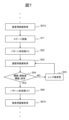
前記試料には複数の検査点が設定され、
前記複数の検査点のいずれかが観察視野に含まれるように前記ステージを移動させ、
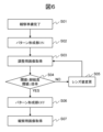
前記光学系が備えるパターン形成部をONとして、前記励起光が前記試料の表面に光学パターンを形成した状態での光電子像である調整用画像を取得し、前記調整用画像において前記光学パターンによって形成された明暗パターンの特徴量に基づき前記電子光学系の調整を行い、
前記光学系が備えるパターン形成部をOFFとして、前記励起光が前記試料の表面に前記光学パターンを形成しない状態での光電子像である検査用画像を取得する検査方法。 - 請求項12において、
前記調整用画像の前記明暗パターンの鮮鋭度が所定の閾値を満たすように前記電子光学系のフォーカスを調整する検査方法。 - 請求項13において、
前記制御部は、前記光学パターンの寸法をあらかじめ記憶しており、前記調整用画像の前記明暗パターンとあらかじめ記憶している前記光学パターンの寸法とに基づき、前記調整用画像の倍率を算出する検査方法。 - 請求項14において、
前記調整用画像の倍率が一定となるように、前記調整用画像の倍率に基づき前記電子光学系の倍率調整を行う、または前記調整用画像の倍率に基づき前記検査用画像の拡大もしくは縮小を行う画像処理を行う検査方法。
Priority Applications (3)
| Application Number | Priority Date | Filing Date | Title |
|---|---|---|---|
| JP2021144394A JP7635103B2 (ja) | 2021-09-06 | 2021-09-06 | 電子線応用装置及び検査方法 |
| US17/878,113 US20230071801A1 (en) | 2021-09-06 | 2022-08-01 | Electron beam application apparatus and inspection method |
| DE102022121795.7A DE102022121795A1 (de) | 2021-09-06 | 2022-08-29 | Elektronenstrahl-anwendungsvorrichtung und prüfverfahren |
Applications Claiming Priority (1)
| Application Number | Priority Date | Filing Date | Title |
|---|---|---|---|
| JP2021144394A JP7635103B2 (ja) | 2021-09-06 | 2021-09-06 | 電子線応用装置及び検査方法 |
Publications (2)
| Publication Number | Publication Date |
|---|---|
| JP2023037678A JP2023037678A (ja) | 2023-03-16 |
| JP7635103B2 true JP7635103B2 (ja) | 2025-02-25 |
Family
ID=85226586
Family Applications (1)
| Application Number | Title | Priority Date | Filing Date |
|---|---|---|---|
| JP2021144394A Active JP7635103B2 (ja) | 2021-09-06 | 2021-09-06 | 電子線応用装置及び検査方法 |
Country Status (3)
| Country | Link |
|---|---|
| US (1) | US20230071801A1 (ja) |
| JP (1) | JP7635103B2 (ja) |
| DE (1) | DE102022121795A1 (ja) |
Citations (5)
| Publication number | Priority date | Publication date | Assignee | Title |
|---|---|---|---|---|
| JP2000081400A (ja) | 1998-09-04 | 2000-03-21 | Canon Inc | 光電子顕微鏡装置 |
| JP2000340161A (ja) | 1999-05-27 | 2000-12-08 | Canon Inc | 光電子顕微鏡装置 |
| JP2004265652A (ja) | 2003-02-28 | 2004-09-24 | Ricoh Co Ltd | 光電子顕微鏡の電子レンズ調整標準及びその製造方法 |
| US20080302974A1 (en) | 2007-06-06 | 2008-12-11 | Hermes-Microvision, Inc. | Optical auto focusing system and method for electron beam inspection tool |
| US20200152415A1 (en) | 2018-11-08 | 2020-05-14 | Hitachi High-Technologies Corporation | Electron Beam Device |
Family Cites Families (7)
| Publication number | Priority date | Publication date | Assignee | Title |
|---|---|---|---|---|
| JPH04277457A (ja) * | 1991-03-06 | 1992-10-02 | Jeol Ltd | 電子プローブマイクロアナライザにおける試料位置設定方法 |
| JP2648538B2 (ja) * | 1991-10-25 | 1997-09-03 | 浜松ホトニクス株式会社 | 2次元の電子源を利用した検査装置 |
| JP3687262B2 (ja) * | 1997-03-26 | 2005-08-24 | 株式会社ニコン | 検査装置のレンズ電圧設定方法及び検査装置 |
| US7348566B2 (en) | 2006-02-28 | 2008-03-25 | International Business Machines Corporation | Aberration-correcting cathode lens microscopy instrument |
| JP5325522B2 (ja) * | 2008-10-15 | 2013-10-23 | 株式会社堀場製作所 | 複合型観察装置 |
| US10146041B1 (en) * | 2018-05-01 | 2018-12-04 | Nanotronics Imaging, Inc. | Systems, devices and methods for automatic microscope focus |
| CN112309808B (zh) * | 2020-11-13 | 2021-12-28 | 中国科学院物理研究所 | 光学聚焦和焦斑连续扫描的透射电子显微镜样品杆系统 |
-
2021
- 2021-09-06 JP JP2021144394A patent/JP7635103B2/ja active Active
-
2022
- 2022-08-01 US US17/878,113 patent/US20230071801A1/en active Pending
- 2022-08-29 DE DE102022121795.7A patent/DE102022121795A1/de active Pending
Patent Citations (6)
| Publication number | Priority date | Publication date | Assignee | Title |
|---|---|---|---|---|
| JP2000081400A (ja) | 1998-09-04 | 2000-03-21 | Canon Inc | 光電子顕微鏡装置 |
| JP2000340161A (ja) | 1999-05-27 | 2000-12-08 | Canon Inc | 光電子顕微鏡装置 |
| JP2004265652A (ja) | 2003-02-28 | 2004-09-24 | Ricoh Co Ltd | 光電子顕微鏡の電子レンズ調整標準及びその製造方法 |
| US20080302974A1 (en) | 2007-06-06 | 2008-12-11 | Hermes-Microvision, Inc. | Optical auto focusing system and method for electron beam inspection tool |
| US20200152415A1 (en) | 2018-11-08 | 2020-05-14 | Hitachi High-Technologies Corporation | Electron Beam Device |
| JP2020077529A (ja) | 2018-11-08 | 2020-05-21 | 株式会社日立ハイテク | 電子線装置 |
Also Published As
| Publication number | Publication date |
|---|---|
| JP2023037678A (ja) | 2023-03-16 |
| US20230071801A1 (en) | 2023-03-09 |
| DE102022121795A1 (de) | 2023-03-09 |
Similar Documents
| Publication | Publication Date | Title |
|---|---|---|
| KR102175027B1 (ko) | 오버레이 계측의 콘트라스트 증강을 위한 구조화 조명 | |
| US10007100B2 (en) | Light sheet illumination microscope and light sheet illumination method | |
| KR20170103418A (ko) | 패턴광 조사 장치 및 방법 | |
| WO2006038439A1 (ja) | 焦点位置制御機構付き観察装置 | |
| CN113820916B (zh) | 用于表征微光刻掩模的设备和方法 | |
| JP5434352B2 (ja) | 表面検査装置および表面検査方法 | |
| KR102160025B1 (ko) | 하전 입자빔 장치 및 광학식 검사 장치 | |
| US11965835B2 (en) | Apparatus and method for gray field imaging | |
| JP7635103B2 (ja) | 電子線応用装置及び検査方法 | |
| JP7382904B2 (ja) | マイクロリソグラフィ用マスクを測定するためのデバイス、および自動合焦方法 | |
| JP4879619B2 (ja) | レーザ加工装置 | |
| US10677743B1 (en) | Inspection apparatus and inspection method | |
| JP2021006903A5 (ja) | ||
| KR102803579B1 (ko) | 웨이퍼 내부의 결함 검사장치 및 웨이퍼 내부의 결함 검사방법 | |
| JP7772377B2 (ja) | サンプル上に複数の荷電粒子ビームレットのアレイを投影するための装置及び方法 | |
| US9091525B2 (en) | Method for focusing an object plane and optical assembly | |
| KR20200019386A (ko) | 레이저 가공 장치 | |
| US12135295B2 (en) | Inspection apparatus and focal position adjustment method | |
| KR101924888B1 (ko) | 마이켈슨 간섭계와 이것을 이용한 간섭무늬 획득방법 | |
| JP6893842B2 (ja) | パターン検査方法およびパターン検査装置 | |
| JP2015225288A (ja) | オートフォーカス装置及びオートフォーカス方法 | |
| JP4034759B2 (ja) | 顕微鏡用照明調整方法及び顕微鏡 | |
| KR102066129B1 (ko) | 도트 어레이를 이용하는 3차원 정보 생성 장치 및 방법 | |
| KR102355523B1 (ko) | 슬릿광원 및 이를 포함하는 비전검사장치 | |
| JP6424043B2 (ja) | 照明装置、光学検査装置及び光学顕微鏡 |
Legal Events
| Date | Code | Title | Description |
|---|---|---|---|
| A621 | Written request for application examination |
Free format text: JAPANESE INTERMEDIATE CODE: A621 Effective date: 20240206 |
|
| A977 | Report on retrieval |
Free format text: JAPANESE INTERMEDIATE CODE: A971007 Effective date: 20241217 |
|
| TRDD | Decision of grant or rejection written | ||
| A01 | Written decision to grant a patent or to grant a registration (utility model) |
Free format text: JAPANESE INTERMEDIATE CODE: A01 Effective date: 20250204 |
|
| A61 | First payment of annual fees (during grant procedure) |
Free format text: JAPANESE INTERMEDIATE CODE: A61 Effective date: 20250212 |
|
| R150 | Certificate of patent or registration of utility model |
Ref document number: 7635103 Country of ref document: JP Free format text: JAPANESE INTERMEDIATE CODE: R150 |