JP7635103B2 - Electron beam application device and inspection method - Google Patents
Electron beam application device and inspection method Download PDFInfo
- Publication number
- JP7635103B2 JP7635103B2 JP2021144394A JP2021144394A JP7635103B2 JP 7635103 B2 JP7635103 B2 JP 7635103B2 JP 2021144394 A JP2021144394 A JP 2021144394A JP 2021144394 A JP2021144394 A JP 2021144394A JP 7635103 B2 JP7635103 B2 JP 7635103B2
- Authority
- JP
- Japan
- Prior art keywords
- optical
- pattern
- excitation light
- sample
- light
- Prior art date
- Legal status (The legal status is an assumption and is not a legal conclusion. Google has not performed a legal analysis and makes no representation as to the accuracy of the status listed.)
- Active
Links
Images


Classifications
-
- H—ELECTRICITY
- H01—ELECTRIC ELEMENTS
- H01J—ELECTRIC DISCHARGE TUBES OR DISCHARGE LAMPS
- H01J37/00—Discharge tubes with provision for introducing objects or material to be exposed to the discharge, e.g. for the purpose of examination or processing thereof
- H01J37/02—Details
- H01J37/04—Arrangements of electrodes and associated parts for generating or controlling the discharge, e.g. electron-optical arrangement or ion-optical arrangement
- H01J37/10—Lenses
-
- G—PHYSICS
- G01—MEASURING; TESTING
- G01N—INVESTIGATING OR ANALYSING MATERIALS BY DETERMINING THEIR CHEMICAL OR PHYSICAL PROPERTIES
- G01N23/00—Investigating or analysing materials by the use of wave or particle radiation, e.g. X-rays or neutrons, not covered by groups G01N3/00 – G01N17/00, G01N21/00 or G01N22/00
- G01N23/22—Investigating or analysing materials by the use of wave or particle radiation, e.g. X-rays or neutrons, not covered by groups G01N3/00 – G01N17/00, G01N21/00 or G01N22/00 by measuring secondary emission from the material
- G01N23/227—Measuring photoelectric effect, e.g. photoelectron emission microscopy [PEEM]
-
- H—ELECTRICITY
- H01—ELECTRIC ELEMENTS
- H01J—ELECTRIC DISCHARGE TUBES OR DISCHARGE LAMPS
- H01J37/00—Discharge tubes with provision for introducing objects or material to be exposed to the discharge, e.g. for the purpose of examination or processing thereof
- H01J37/02—Details
- H01J37/21—Means for adjusting the focus
-
- H—ELECTRICITY
- H01—ELECTRIC ELEMENTS
- H01J—ELECTRIC DISCHARGE TUBES OR DISCHARGE LAMPS
- H01J37/00—Discharge tubes with provision for introducing objects or material to be exposed to the discharge, e.g. for the purpose of examination or processing thereof
- H01J37/02—Details
- H01J37/22—Optical, image processing or photographic arrangements associated with the tube
- H01J37/226—Optical arrangements for illuminating the object; optical arrangements for collecting light from the object
-
- H—ELECTRICITY
- H01—ELECTRIC ELEMENTS
- H01J—ELECTRIC DISCHARGE TUBES OR DISCHARGE LAMPS
- H01J37/00—Discharge tubes with provision for introducing objects or material to be exposed to the discharge, e.g. for the purpose of examination or processing thereof
- H01J37/26—Electron or ion microscopes; Electron or ion diffraction tubes
- H01J37/285—Emission microscopes, e.g. field-emission microscopes
-
- H—ELECTRICITY
- H01—ELECTRIC ELEMENTS
- H01J—ELECTRIC DISCHARGE TUBES OR DISCHARGE LAMPS
- H01J2237/00—Discharge tubes exposing object to beam, e.g. for analysis treatment, etching, imaging
- H01J2237/26—Electron or ion microscopes
- H01J2237/285—Emission microscopes
- H01J2237/2855—Photo-emission
Landscapes
- Chemical & Material Sciences (AREA)
- Analytical Chemistry (AREA)
- Physics & Mathematics (AREA)
- Health & Medical Sciences (AREA)
- Life Sciences & Earth Sciences (AREA)
- Biochemistry (AREA)
- General Health & Medical Sciences (AREA)
- General Physics & Mathematics (AREA)
- Immunology (AREA)
- Pathology (AREA)
- Analysing Materials By The Use Of Radiation (AREA)
Description
本発明は、電子線応用装置及びそれを用いた検査方法に関する。 The present invention relates to an electron beam application device and an inspection method using the same.
光電子顕微鏡(Photoelectron Emission Microscope:PEEM)は、紫外光やX線(励起光)を試料の表面に照射することによって発生する光電子を用いて像を形成する装置であり、試料の表面構造に起因するコントラストを有する光電子像を得ることができる。 A photoelectron emission microscope (PEEM) is an instrument that forms an image using photoelectrons generated by irradiating the surface of a sample with ultraviolet light or X-rays (excitation light), and can obtain a photoelectron image with contrast resulting from the surface structure of the sample.
特許文献1には、カソード・レンズ顕微鏡(PEEMはその一例である)の構造の一例が開示されている。 Patent document 1 discloses an example of the structure of a cathode lens microscope (PEEM is one example).
PEEMの電子光学系では、光電子像を結像レンズ系によりカメラに投影する。観察試料の高さが異なると、光電子像のフォーカスをあわせるために対物レンズの強度(焦点距離)を変更する必要がある。これにより、結像レンズ系の物面に形成される光電子像の大きさが変化し、この結果、カメラ(結像レンズ系の像面)に投影される光電子像の大きさが変化してしまう。 In the electron optical system of a PEEM, a photoelectron image is projected onto a camera by an imaging lens system. If the height of the observed sample differs, the strength (focal length) of the objective lens must be changed to focus the photoelectron image. This changes the size of the photoelectron image formed on the object plane of the imaging lens system, which in turn changes the size of the photoelectron image projected onto the camera (the image plane of the imaging lens system).
フォーカス調整に伴う光電子像の大きさの変化をなくすためには、例えば、フォーカス調整を標準試料、または、観察試料上の大きさが既知であるパターンの光電子像を取得することで、得られた光電子像の倍率を把握し、所定の倍率になるよう光電子像の倍率を調整すればよい。しかしながら、この方法では倍率の調整のために観察視野の移動が必要となり、時間がかかる。また、光電子像の倍率を精度よく算出するためには、高いコントラストをもつ光電子像を得る必要がある。 To eliminate the change in size of the photoelectron image that accompanies focus adjustment, for example, the focus can be adjusted by obtaining a photoelectron image of a standard sample or a pattern of a known size on the observation sample, determining the magnification of the obtained photoelectron image, and adjusting the magnification of the photoelectron image to a specified magnification. However, this method requires moving the observation field to adjust the magnification, which is time-consuming. Also, to accurately calculate the magnification of the photoelectron image, it is necessary to obtain a photoelectron image with high contrast.
本発明の一実施の態様である電子線応用装置は、試料に励起光を照射する光学系と、励起光が照射された試料から放出される光電子による光電子像をカメラに投影する電子光学系と、制御部とを有し、光学系は励起光を発生させる光源とパターン形成部とを備え、パターン形成部がONのときには励起光は試料の表面に光学パターンを形成し、パターン形成部がOFFのときには、励起光は、試料の表面に光学パターンを形成することなく、試料に照射され、制御部は、パターン形成部をONとして得られた光電子像において光学パターンによって形成された明暗パターンの特徴量に基づき電子光学系の調整を行う。 An electron beam application device according to one embodiment of the present invention has an optical system that irradiates a sample with excitation light, an electron optical system that projects a photoelectron image formed by photoelectrons emitted from the sample irradiated with the excitation light onto a camera, and a control unit. The optical system includes a light source that generates excitation light and a pattern forming unit. When the pattern forming unit is ON, the excitation light forms an optical pattern on the surface of the sample, and when the pattern forming unit is OFF, the excitation light is irradiated onto the sample without forming an optical pattern on the surface of the sample. The control unit adjusts the electron optical system based on the feature amount of the light-dark pattern formed by the optical pattern in the photoelectron image obtained with the pattern forming unit ON.
投影型電子線応用装置の電子光学系の調整を高速かつ高精度に実施可能とする。その他の課題と新規な特徴は、本明細書の記述および添付図面から明らかになるであろう。 This enables the adjustment of the electron optical system of a projection type electron beam application device to be performed quickly and with high precision. Other objects and novel features will become apparent from the description of this specification and the accompanying drawings.
図1に本実施例の電子線応用装置の構成例を示す。図1は、レーザ光やX線などの励起光を試料の表面に照射して発生する光電子による像(光電子像)を得るPEEMを例示している。装置本体10は、その主要な構成として、試料4を載置するステージ7、励起光5を試料4に照射する光学系1、光電子像を撮影するカメラ3、光電子像をカメラ3に投影する電子光学系2を有している。光学系1は、励起光5を発生させる光源11とパターン形成部12とを備えている。パターン形成部12は、光源11からの励起光5をパターン光として試料4に照射し、試料4の表面に光学パターンを形成する。詳細については後述するが、パターン形成部12をONすることでパターン光が、パターン形成部12をOFFすることで試料表面に光学パターンを形成しない光(以下では均一光とよぶ)が光学系1から試料4に照射される。その他、光学系1は励起光5を試料4に照射するために、レンズやミラーなどの光学素子を備える場合もある。励起光5を試料4に照射することにより発生した光電子6による光電子像は電子光学系2によりカメラ3に投影される。図1では電子光学系2は電子レンズに代表させて表示しているが、1段以上の電子レンズ、その他の電子光学素子を備えている。カメラ3は光電子そのものを検知して撮影するものであってもよいし、シンチレータを備え、シンチレータによって電子を一旦光に変換し、変換された光を検知して撮影するものであってもよい。
Figure 1 shows an example of the configuration of the electron beam application device of this embodiment. Figure 1 illustrates a PEEM that obtains an image (photoelectron image) by photoelectrons generated by irradiating the surface of a sample with excitation light such as laser light or X-rays. The main components of the
装置本体10は制御部20と接続されている。制御部20は、GUI(Graphical User Interface)装置22から入力されるユーザからの指示を受けて装置本体10の制御を行うとともに、カメラ3で撮影された光電子像の画像処理を行う。制御部20は記憶部21を備え、記憶部21には、装置本体10の制御パラメータや、光電子像が記憶される。
The
以下に、パターン形成部12が試料4上に照射するパターン光について説明する。パターン光により形成される光学パターンの第1の例は、光源11からの励起光をパターン形成部12により複数の励起光に分岐させ、それらが互いに干渉することによって発生する干渉縞である。図2Aは、パターン形成部12が1次元の光路差を形成したときに得られる干渉縞の模式図であり、励起光5の強度が試料表面上でストライプパターンをなすように変化している。図2Bは、パターン形成部12が2次元の光路差を形成したときに得られる干渉縞の模式図であり、励起光5の強度が試料表面上で同心円パターンをなすように変化している。
The pattern light that the
図3A~図3Cに、試料表面に干渉縞を形成するパターン形成部12の構成例を示す。図3Aは、パターン形成部12に光学平面をもつ光学素子30を用いる例である。パターン形成部12をONする場合には、光学素子30を励起光の光路に挿入する。励起光が光学素子30の入射面31と出射面32との間で多重反射することにより、光路差をもつ光に分岐され、干渉縞が生じる。パターン形成部12をOFFする場合には、光学素子30を励起光の光路の外へ移動させる。なお、図では入射面31と出射面32との反射に角度をつけて表示しているが、これは多重反射している様子を分かりやすく示すためのものである。光学素子30の光学平面が光路に対して垂直に配置される場合には、出射面32からの反射光は出射面32と垂直な方向に反射されるため、図3Aに示されているような光学素子30を透過した光と光学素子30内で反射した光との間に位置ずれは発生しない。
Figures 3A to 3C show examples of the configuration of the
図3Bは、光路分岐によって光路差を発生させる光学アセンブリ40を用いる例である。光学アセンブリ40は入射した光を複数の光路に分岐させ、再度合流させて出射させる。図3Bの例では、光学アセンブリ40は、可動するハーフミラー41a,41bと固定されたミラー42a,42bとを有する。パターン形成部12をONする場合には、ハーフミラー41a,41bを励起光の光路に挿入する。ハーフミラー41a,41bが励起光の光路に挿入されることにより、ハーフミラー41aにより、ハーフミラー41aを透過する光と反射する光に分岐される。透過光43はハーフミラー41bを透過し、光学アセンブリ40から出射される。一方、反射光44は、ミラー42a、ミラー42b、ハーフミラー41bで反射され、透過光43と合流して光学アセンブリ40から出射される。光路差をもつ励起光が干渉することにより、干渉縞が生じる。パターン形成部12をOFFする場合には、ハーフミラー41a,41bを励起光の光路の外へ移動させる。
3B is an example of using an
図3Cは可動ミラー50を用いる例である。パターン形成部12をONする場合には、可動ミラー50を、励起光5が試料4で反射した反射光51の光路と垂直となるように配置し、可動ミラー50の反射光52と励起光5とを干渉させて干渉縞を生じさせる。パターン形成部12をOFFする場合には、可動ミラー50を反射光51の光路の外へ移動させる。
Figure 3C shows an example in which a
パターン光により形成される光学パターンの第2の例では、光源11からの励起光をパターン(マスクパターンという)が形成された光学マスクに透過または反射させ、マスクパターンを試料4に投影する。光学マスクとしては透過型マスクまたは反射型マスクが使用でき、光学マスクのマスクパターンが試料4上で結像するよう、パターン形成部12はレンズまたはミラーを含む投影光学系を備える。図4Aは透過型マスク60と投影レンズ61により、透過型マスク60に形成されているマスクパターンを試料4に投影させるパターン形成部12の構成例を示している。
In a second example of an optical pattern formed by pattern light, excitation light from the
図4Bに図4Aに示した透過型マスク60に形成されるマスクパターン例を示す。励起光を透過させる透過部63と励起光を遮蔽する遮蔽部64により市松模様が形成されている。反射型マスクであっても反射部と透過部とを同様に設けることで、試料4上に同じパマスクパターンを投影することが可能である。マスクパターンの形状については限定されないが、後述するように光学パターンによって形成される明暗パターンの特徴量を用いて電子光学系を調整するため、ラインエッジを多く含む2値パターンとすることが望ましい。
Figure 4B shows an example of a mask pattern formed on the
パターン形成部12をONする場合には、光源11からの励起光の光路上に光学マスクを挿入する。パターン形成部12をOFFする場合には、光学マスクを励起光の光路の外へ移動させてもよいし、光源11から光学マスクを通ることなく試料4に励起光を照射する迂回路をあらかじめ設けておき、励起光の光路を迂回路に切り替えるようにしてもよい。
When the
図5を用いてパターン形成部12をON,OFFしたときの光電子像について説明する。光電子像70はパターン形成部をOFFとしたとき(観察時)の光電子像である。光学系1は、パターン形成部12がOFFとされている場合には、光源11からの励起光が均一に試料4に照射されるように調整されている。試料4に材料または構造が異なる領域が存在すると、励起光5が照射されたことにより発生する光電子の放出確率が当該領域と他の領域とで異なる。光電子の放出確率の違いが光電子像のコントラストとなって、光電子像が得られる。
Using Figure 5, the photoelectron image when the
光電子像70における領域72は、試料4の表面における材料や構造が異なる領域を反映している。照射する励起光の強度が高い程、明るい光電子像が得られるため、励起光5として均一光を照射するときの励起光強度をA、試料表面における光電子放出確率をP(x,y)、光電子像70の輝度をI1(x,y)とするとき、
I1(x,y)=A・P(x,y)
と表現できる。
I 1 (x, y) = A・P (x, y)
This can be expressed as follows.
一方、パターン形成部12がONとされ、励起光5としてパターン光を照射するとき、励起光強度が照射位置によって異なることになるため、励起光強度をA(x,y)、光電子像71の輝度をI2(x,y)とするとき、
I2(x,y)=A(x,y)・P(x,y)
と表現できる。
On the other hand, when the
I 2 (x,y)=A(x,y)・P(x,y)
This can be expressed as follows.
パターン光の励起光強度A(x,y)のとりうる値は、理想的には最大値がA(均一光を照射するときの励起光強度)、最小値を0(励起光が照射されない状態)とできるため、光学パターンによって形成される明暗パターンのコントラストは、試料の材料や構造による光電子放出確率P(x,y)によって生じるコントラストよりも大きなコントラストを得ることができる。したがって、試料4の試料表面の材料や構造にかかわらず、光電子像71において光学パターンによって形成される明暗パターン73は観察が容易であり、解析も精度よく行える。本実施例ではこのことを利用して、第1に、明暗パターン73の鮮鋭度に基づき電子光学系2のフォーカス調整を行う。光学パターンによって形成される明暗パターンは高コントラストであるため、フォーカス調整を容易に、また精度よく行える。第2に、試料上の光学パターンの寸法と光電子像71における明暗パターン73とに基づき、光電子像の倍率を算出する。光学パターンによって形成される明暗パターンは高コントラストであるため、光電子像の倍率算出も容易に、また精度よく行える。パターン光によって形成される試料上の光学パターンの寸法はあらかじめ求めておき、記憶部21に記憶しておく。
Ideally, the possible values of the excitation light intensity A(x, y) of the pattern light can be set to a maximum value of A (excitation light intensity when uniform light is irradiated) and a minimum value of 0 (state where excitation light is not irradiated), so the contrast of the light-dark pattern formed by the optical pattern can be greater than the contrast caused by the photoelectron emission probability P(x, y) due to the material and structure of the sample. Therefore, regardless of the material and structure of the sample surface of the
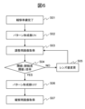
図6に電子線応用装置による観察のフローチャートを示す。本フローは制御部20により制御される。まず、観察準備を行う(S01)。観察準備完了した段階で、観察視野に観察したい試料表面の位置がとらえられていればよい。次に、制御部20はパターン形成部12をONとし(S02)、調整用画像を取得する(S03)。調整用画像は例えば、光電子像71(図5参照)のような光電子像である。調整用画像の明暗パターンから光電子像の鮮鋭度と倍率とを算出し、あらかじめ定めてある閾値と比較する(S04)。
Figure 6 shows a flowchart of observation using an electron beam application device. This flow is controlled by the
明暗パターンが例えば光電子像71の明暗パターン73のようなラインパターンである場合には、鮮鋭度の指標としてラインパターンのエッジにおける輝度変化を用いることができる。例えば、エッジ部分における輝度変化が急峻であれば鮮鋭度が高く、緩やかであれば鮮鋭度が低いと判断できる。また、調整用画像に含まれるラインパターンの本数をカウントすることにより、ラインパターンに対応する光学パターンの寸法が既知であるので、調整用画像に写っている領域の実寸を算出できる。実寸と調整用画像の大きさから倍率を算出することができる。
When the light and dark pattern is a line pattern such as light and
調整用画像の鮮鋭度と倍率とが所望の閾値を満たさない場合には、電子光学系2のレンズ値を変更し、倍率調整やフォーカス調整を行う(S05)。調整用画像の鮮鋭度と倍率とが所望の閾値を満たしている場合には、パターン形成部をOFFとし(S06)、観察用画像を取得する(S07)。観察用画像は例えば、光電子像70(図5参照)のような光電子像である。電子光学系の調整を明暗パターンで行うことにより、試料表面の光電子像を所望の倍率で、鮮明な光電子像として取得することができる。
If the sharpness and magnification of the adjustment image do not meet the desired thresholds, the lens value of the electron
PEEMは一般的には試料の分析を目的とする観察に用いられるが、現在、光を用いる光学式検査装置、電子線を用いるSEM(Scanning Electron Microscope)式検査装置が広く用いられている、半導体ウエハの表面に形成されたパターン形状の検査装置として、PEEMが利用できると考えられる。光学パターンによって形成される明暗パターンを用いて電子光学系の調整を高速かつ高精度で実施する本実施例は、PEEM式検査装置に対して極めて有効である。 PEEM is generally used for observations aimed at analyzing samples, but currently optical inspection devices that use light and SEM (Scanning Electron Microscope) type inspection devices that use electron beams are widely used, and it is thought that PEEM can be used as an inspection device for the pattern shapes formed on the surface of semiconductor wafers. This embodiment, which adjusts the electron optical system quickly and with high precision using the light and dark patterns formed by the optical pattern, is extremely effective for PEEM type inspection devices.
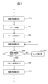
図7にPEEM式検査装置による検査のフローチャートを示す。本フローも制御部20により制御される。図6のフローチャートと同じ処理については同じ符号を付して、重複する説明は省略する。半導体ウエハには複数の検査点が設定されており、ある検査点に対する検査用画像が取得(S07a)された後、次の検査点にステージ移動する(S11)。制御部20はパターン形成部12をONとし(S02)、調整用画像を取得する(S03)。調整用画像の明暗パターンから光電子像の鮮鋭度と倍率とを算出し、あらかじめ定めてある閾値と比較する(S04)。
Figure 7 shows a flowchart of inspection using a PEEM inspection device. This flow is also controlled by the
調整用画像の鮮鋭度と倍率とが所望の閾値を満たさない場合には、電子光学系2のレンズ値を変更し、倍率調整やフォーカス調整を行う(S05)。調整用画像の鮮鋭度と倍率とが所望の閾値を満たしている場合には、パターン形成部をOFFとし(S06)、検査用画像を取得する(S07b)。その後、次の検査点にステージ移動する。
If the sharpness and magnification of the adjustment image do not satisfy the desired thresholds, the lens value of the electro-
上述したように、フォーカス調整を行うことにより、当該検査点での検査用画像の倍率が変化する。レンズ値変更ステップ(S05)において、検査用画像が一定の倍率になるようにレンズ値を調整してもよい。あるいは、倍率が所定の範囲内であれば、各検査点での検査用画像の倍率をあわせるためのレンズ値の調整を行わなくてもよい。これにより検査用画像取得のスループットを向上させることができる。倍率調整のためのレンズ値変更を行わない代わりに、倍率に基づき、画像処理によって得られた検査用画像を拡大または縮小処理してもよいし、検査用画像に対する画像処理をおこなうことなく、検査における良否判定を検査用画像の倍率を考慮して行うようにしてもよい。 As described above, by adjusting the focus, the magnification of the inspection image at the inspection point changes. In the lens value changing step (S05), the lens value may be adjusted so that the inspection image has a constant magnification. Alternatively, if the magnification is within a predetermined range, it is not necessary to adjust the lens value to match the magnification of the inspection image at each inspection point. This can improve the throughput of acquiring the inspection image. Instead of changing the lens value to adjust the magnification, the inspection image obtained by image processing may be enlarged or reduced based on the magnification, or the inspection may be judged as pass/fail without performing image processing on the inspection image and taking into account the magnification of the inspection image.
1:光学系、2:電子光学系、3:カメラ、4:試料、5:励起光、6:光電子、7:ステージ、10:装置本体、11:光源、12:パターン形成部、20:制御部、21:記憶部、22:GUI装置、30:光学素子、31:入射面、32:出射面、40:光学アセンブリ、41a,41b:ハーフミラー、42a,42b:ミラー、43:透過光、44:反射光、50:可動ミラー、51,52:反射光、60:透過型マスク、61:投影レンズ、63:透過部、64:遮蔽部、70,71:光電子像、72:領域、73:明暗パターン。 1: Optical system, 2: Electro-optical system, 3: Camera, 4: Sample, 5: Excitation light, 6: Photoelectrons, 7: Stage, 10: Device body, 11: Light source, 12: Pattern forming section, 20: Control section, 21: Memory section, 22: GUI device, 30: Optical element, 31: Incident surface, 32: Exit surface, 40: Optical assembly, 41a, 41b: Half mirror, 42a, 42b: Mirror, 43: Transmitted light, 44: Reflected light, 50: Movable mirror, 51, 52: Reflected light, 60: Transmissive mask, 61: Projection lens, 63: Transmitting section, 64: Shielding section, 70, 71: Photoelectron image, 72: Area, 73: Bright and dark pattern.
Claims (15)
前記励起光が照射された前記試料から放出される光電子による光電子像をカメラに投影する電子光学系と、
制御部とを有し、
前記光学系は前記励起光を発生させる光源とパターン形成部とを備え、前記パターン形成部がONのときには前記励起光は前記試料の表面に光学パターンを形成し、前記パターン形成部がOFFのときには、前記励起光は、前記試料の表面に前記光学パターンを形成することなく、前記試料に照射され、
前記制御部は、前記パターン形成部をONとして得られた光電子像において前記光学パターンによって形成された明暗パターンの特徴量に基づき前記電子光学系の調整を行う電子線応用装置。 an optical system for irradiating the sample with excitation light;
an electron optical system that projects a photoelectron image formed by photoelectrons emitted from the sample irradiated with the excitation light onto a camera;
A control unit,
the optical system includes a light source that generates the excitation light and a pattern forming unit, and when the pattern forming unit is ON, the excitation light forms an optical pattern on a surface of the sample, and when the pattern forming unit is OFF, the excitation light is irradiated onto the sample without forming the optical pattern on the surface of the sample;
The control unit adjusts the electron optical system based on a feature amount of a light-dark pattern formed by the optical pattern in a photoelectron image obtained by turning on the pattern forming unit.
前記制御部は、前記明暗パターンの鮮鋭度が所定の閾値を満たすように前記電子光学系のフォーカスを調整する電子線応用装置。 In claim 1,
The control unit adjusts the focus of the electron optical system so that the sharpness of the light and dark pattern satisfies a predetermined threshold value.
前記制御部は、前記光学パターンの寸法をあらかじめ記憶しており、前記明暗パターンとあらかじめ記憶している前記光学パターンの寸法とに基づき、前記光電子像の倍率を算出する電子線応用装置。 In claim 1,
The control unit pre-stores dimensions of the optical pattern, and calculates a magnification of the photoelectron image based on the light-dark pattern and the pre-stored dimensions of the optical pattern.
前記制御部は、前記光電子像の倍率が所定の閾値を満たすように前記電子光学系の倍率を調整する電子線応用装置。 In claim 3,
The control unit adjusts the magnification of the electron optical system so that the magnification of the photoelectron image satisfies a predetermined threshold value.
前記光学パターンは干渉縞であり、前記干渉縞は、前記光源からの励起光を前記パターン形成部が光路差をもつ複数の励起光に分岐させ、前記複数の励起光が互いに干渉することにより発生する電子線応用装置。 In claim 1,
The optical pattern is an interference fringe, which is generated when the pattern forming unit branches the excitation light from the light source into multiple excitation light beams having optical path differences, and the multiple excitation light beams interfere with each other.
前記パターン形成部は、光学平面をもつ光学素子を含み、前記パターン形成部がONのときに前記光学素子は前記励起光の光路に挿入され、前記パターン形成部がOFFのときに前記光学素子は前記励起光の光路の外に配置される電子線応用装置。 In claim 5,
The pattern forming unit includes an optical element having an optical plane, and when the pattern forming unit is ON, the optical element is inserted into the optical path of the excitation light, and when the pattern forming unit is OFF, the optical element is positioned outside the optical path of the excitation light.
前記パターン形成部は、入射した光を複数の光路に分岐させ、再度合流させて出射する光学アセンブリを含み、前記パターン形成部がONのときに前記光学アセンブリは前記励起光を前記複数の光路に分岐させ、再度合流させて出射し、前記パターン形成部がOFFのときに前記光学アセンブリは前記励起光を前記複数の光路に分岐させることなく、そのまま出射する電子線応用装置。 In claim 5,
The pattern forming unit includes an optical assembly that branches incident light into multiple optical paths and then recombines the light to emit, and when the pattern forming unit is ON, the optical assembly branches the excitation light into the multiple optical paths and then recombines the light to emit, and when the pattern forming unit is OFF, the optical assembly emits the excitation light as is without branching it into the multiple optical paths.
前記光学パターンは干渉縞であり、前記干渉縞は、前記励起光が前記試料で反射した反射光をミラーにより前記試料に向けて反射させることにより、前記励起光と前記ミラーからの反射光とが互いに干渉することにより発生する電子線応用装置。 In claim 1,
The optical pattern is an interference fringe, which is generated by reflecting the excitation light reflected by the sample toward the sample using a mirror, causing the excitation light and the reflected light from the mirror to interfere with each other.
前記パターン形成部がONのときに前記ミラーは前記試料からの反射光を前記試料に向けて反射するよう配置され、前記パターン形成部がOFFのときに前記ミラーは前記試料からの反射光の光路の外に配置される電子線応用装置。 In claim 8,
An electron beam application device in which, when the pattern forming unit is ON, the mirror is positioned to reflect the reflected light from the sample toward the sample, and, when the pattern forming unit is OFF, the mirror is positioned outside the optical path of the reflected light from the sample.
前記パターン形成部は、マスクパターンが形成された光学マスクと前記マスクパターンを前記試料に投影する投影光学系とを備え、前記光学パターンは、前記試料の表面に投影された前記マスクパターンである電子線応用装置。 In claim 1,
An electron beam application device, wherein the pattern forming unit includes an optical mask on which a mask pattern is formed and a projection optical system that projects the mask pattern onto the sample, and the optical pattern is the mask pattern projected onto the surface of the sample.
前記パターン形成部がONのときに前記光学マスクは前記励起光を透過もしくは反射するよう配置され、前記パターン形成部がOFFのときに前記光学マスクは前記励起光の光路の外に配置される、または前記励起光の光路を前記光学マスクに対して迂回させる電子線応用装置。 In claim 10,
An electron beam application device in which the optical mask is positioned to transmit or reflect the excitation light when the pattern forming unit is ON, and when the pattern forming unit is OFF, the optical mask is positioned outside the optical path of the excitation light, or the optical path of the excitation light is diverted relative to the optical mask.
前記試料には複数の検査点が設定され、
前記複数の検査点のいずれかが観察視野に含まれるように前記ステージを移動させ、
前記光学系が備えるパターン形成部をONとして、前記励起光が前記試料の表面に光学パターンを形成した状態での光電子像である調整用画像を取得し、前記調整用画像において前記光学パターンによって形成された明暗パターンの特徴量に基づき前記電子光学系の調整を行い、
前記光学系が備えるパターン形成部をOFFとして、前記励起光が前記試料の表面に前記光学パターンを形成しない状態での光電子像である検査用画像を取得する検査方法。 1. An inspection method using an electron beam application device including: a stage for placing a sample; an optical system for irradiating the sample with excitation light; an electron optical system for projecting a photoelectron image formed by photoelectrons emitted from the sample irradiated with the excitation light onto a camera; and a control unit,
A plurality of test points are set on the sample,
moving the stage so that any one of the plurality of inspection points is included in an observation field of view;
a pattern forming unit included in the optical system is turned on to obtain an adjustment image which is a photoelectron image in a state in which the excitation light forms an optical pattern on the surface of the sample, and the electron optical system is adjusted based on a feature amount of a light-dark pattern formed by the optical pattern in the adjustment image;
An inspection method in which a pattern forming section of the optical system is turned off and an inspection image, which is a photoelectron image, is obtained in a state in which the excitation light does not form the optical pattern on the surface of the sample.
前記調整用画像の前記明暗パターンの鮮鋭度が所定の閾値を満たすように前記電子光学系のフォーカスを調整する検査方法。 In claim 12,
An inspection method that adjusts the focus of the electron optical system so that the sharpness of the light and dark pattern of the adjustment image satisfies a predetermined threshold value.
前記制御部は、前記光学パターンの寸法をあらかじめ記憶しており、前記調整用画像の前記明暗パターンとあらかじめ記憶している前記光学パターンの寸法とに基づき、前記調整用画像の倍率を算出する検査方法。 In claim 13,
The control unit pre-stores the dimensions of the optical pattern, and calculates the magnification of the adjustment image based on the light and dark pattern of the adjustment image and the pre-stored dimensions of the optical pattern.
前記調整用画像の倍率が一定となるように、前記調整用画像の倍率に基づき前記電子光学系の倍率調整を行う、または前記調整用画像の倍率に基づき前記検査用画像の拡大もしくは縮小を行う画像処理を行う検査方法。 In claim 14,
An inspection method that performs image processing to adjust the magnification of the electron optical system based on the magnification of the adjustment image so that the magnification of the adjustment image is constant, or to enlarge or reduce the inspection image based on the magnification of the adjustment image.
Priority Applications (3)
| Application Number | Priority Date | Filing Date | Title |
|---|---|---|---|
| JP2021144394A JP7635103B2 (en) | 2021-09-06 | 2021-09-06 | Electron beam application device and inspection method |
| US17/878,113 US20230071801A1 (en) | 2021-09-06 | 2022-08-01 | Electron beam application apparatus and inspection method |
| DE102022121795.7A DE102022121795A1 (en) | 2021-09-06 | 2022-08-29 | ELECTRON BEAM APPLICATION DEVICE AND TEST METHOD |
Applications Claiming Priority (1)
| Application Number | Priority Date | Filing Date | Title |
|---|---|---|---|
| JP2021144394A JP7635103B2 (en) | 2021-09-06 | 2021-09-06 | Electron beam application device and inspection method |
Publications (2)
| Publication Number | Publication Date |
|---|---|
| JP2023037678A JP2023037678A (en) | 2023-03-16 |
| JP7635103B2 true JP7635103B2 (en) | 2025-02-25 |
Family
ID=85226586
Family Applications (1)
| Application Number | Title | Priority Date | Filing Date |
|---|---|---|---|
| JP2021144394A Active JP7635103B2 (en) | 2021-09-06 | 2021-09-06 | Electron beam application device and inspection method |
Country Status (3)
| Country | Link |
|---|---|
| US (1) | US20230071801A1 (en) |
| JP (1) | JP7635103B2 (en) |
| DE (1) | DE102022121795A1 (en) |
Citations (5)
| Publication number | Priority date | Publication date | Assignee | Title |
|---|---|---|---|---|
| JP2000081400A (en) | 1998-09-04 | 2000-03-21 | Canon Inc | Photoelectron microscope |
| JP2000340161A (en) | 1999-05-27 | 2000-12-08 | Canon Inc | Photoelectron microscope |
| JP2004265652A (en) | 2003-02-28 | 2004-09-24 | Ricoh Co Ltd | Electron lens adjustment standard for photoelectron microscope and method of manufacturing the same |
| US20080302974A1 (en) | 2007-06-06 | 2008-12-11 | Hermes-Microvision, Inc. | Optical auto focusing system and method for electron beam inspection tool |
| US20200152415A1 (en) | 2018-11-08 | 2020-05-14 | Hitachi High-Technologies Corporation | Electron Beam Device |
Family Cites Families (7)
| Publication number | Priority date | Publication date | Assignee | Title |
|---|---|---|---|---|
| JPH04277457A (en) * | 1991-03-06 | 1992-10-02 | Jeol Ltd | Method for setting of specimen position in micro-analyzer with electron probe |
| JP2648538B2 (en) * | 1991-10-25 | 1997-09-03 | 浜松ホトニクス株式会社 | Inspection device using two-dimensional electron source |
| JP3687262B2 (en) * | 1997-03-26 | 2005-08-24 | 株式会社ニコン | Lens voltage setting method and inspection apparatus for inspection apparatus |
| US7348566B2 (en) | 2006-02-28 | 2008-03-25 | International Business Machines Corporation | Aberration-correcting cathode lens microscopy instrument |
| JP5325522B2 (en) * | 2008-10-15 | 2013-10-23 | 株式会社堀場製作所 | Combined observation system |
| US10146041B1 (en) * | 2018-05-01 | 2018-12-04 | Nanotronics Imaging, Inc. | Systems, devices and methods for automatic microscope focus |
| CN112309808B (en) * | 2020-11-13 | 2021-12-28 | 中国科学院物理研究所 | Transmission electron microscope sample holder system with optical focusing and continuous scanning of focal spot |
-
2021
- 2021-09-06 JP JP2021144394A patent/JP7635103B2/en active Active
-
2022
- 2022-08-01 US US17/878,113 patent/US20230071801A1/en active Pending
- 2022-08-29 DE DE102022121795.7A patent/DE102022121795A1/en active Pending
Patent Citations (6)
| Publication number | Priority date | Publication date | Assignee | Title |
|---|---|---|---|---|
| JP2000081400A (en) | 1998-09-04 | 2000-03-21 | Canon Inc | Photoelectron microscope |
| JP2000340161A (en) | 1999-05-27 | 2000-12-08 | Canon Inc | Photoelectron microscope |
| JP2004265652A (en) | 2003-02-28 | 2004-09-24 | Ricoh Co Ltd | Electron lens adjustment standard for photoelectron microscope and method of manufacturing the same |
| US20080302974A1 (en) | 2007-06-06 | 2008-12-11 | Hermes-Microvision, Inc. | Optical auto focusing system and method for electron beam inspection tool |
| US20200152415A1 (en) | 2018-11-08 | 2020-05-14 | Hitachi High-Technologies Corporation | Electron Beam Device |
| JP2020077529A (en) | 2018-11-08 | 2020-05-21 | 株式会社日立ハイテク | Electron beam equipment |
Also Published As
| Publication number | Publication date |
|---|---|
| JP2023037678A (en) | 2023-03-16 |
| US20230071801A1 (en) | 2023-03-09 |
| DE102022121795A1 (en) | 2023-03-09 |
Similar Documents
| Publication | Publication Date | Title |
|---|---|---|
| KR102175027B1 (en) | Structured illumination for contrast enhancement in overlay metrology | |
| US10007100B2 (en) | Light sheet illumination microscope and light sheet illumination method | |
| KR20170103418A (en) | Pattern lighting appartus and method thereof | |
| WO2006038439A1 (en) | Observation apparatus with focus position control mechanism | |
| CN113820916B (en) | Apparatus and method for characterizing microlithography masks | |
| JP5434352B2 (en) | Surface inspection apparatus and surface inspection method | |
| KR102160025B1 (en) | Charged particle beam device and optical inspection device | |
| US11965835B2 (en) | Apparatus and method for gray field imaging | |
| JP7635103B2 (en) | Electron beam application device and inspection method | |
| JP7382904B2 (en) | Device for measuring masks for microlithography and automatic focusing method | |
| JP4879619B2 (en) | Laser processing equipment | |
| US10677743B1 (en) | Inspection apparatus and inspection method | |
| JP2021006903A5 (en) | ||
| KR102803579B1 (en) | Apparatus for inspecting defect inside wafer and method of inspecting defect inside wafer | |
| JP7772377B2 (en) | Apparatus and method for projecting an array of charged particle beamlets onto a sample - Patent Application 20070122997 | |
| US9091525B2 (en) | Method for focusing an object plane and optical assembly | |
| KR20200019386A (en) | Laser processing apparatus | |
| US12135295B2 (en) | Inspection apparatus and focal position adjustment method | |
| KR101924888B1 (en) | Michelson interferometer and method for obtaining interference pattern using the same | |
| JP6893842B2 (en) | Pattern inspection method and pattern inspection equipment | |
| JP2015225288A (en) | Autofocus device and autofocus method | |
| JP4034759B2 (en) | Microscope illumination adjustment method and microscope | |
| KR102066129B1 (en) | Apparatus and method for 3d information using dot array | |
| KR102355523B1 (en) | Slit light source and vision inspection apparatus having the same | |
| JP6424043B2 (en) | Illumination device, optical inspection device, and optical microscope |
Legal Events
| Date | Code | Title | Description |
|---|---|---|---|
| A621 | Written request for application examination |
Free format text: JAPANESE INTERMEDIATE CODE: A621 Effective date: 20240206 |
|
| A977 | Report on retrieval |
Free format text: JAPANESE INTERMEDIATE CODE: A971007 Effective date: 20241217 |
|
| TRDD | Decision of grant or rejection written | ||
| A01 | Written decision to grant a patent or to grant a registration (utility model) |
Free format text: JAPANESE INTERMEDIATE CODE: A01 Effective date: 20250204 |
|
| A61 | First payment of annual fees (during grant procedure) |
Free format text: JAPANESE INTERMEDIATE CODE: A61 Effective date: 20250212 |
|
| R150 | Certificate of patent or registration of utility model |
Ref document number: 7635103 Country of ref document: JP Free format text: JAPANESE INTERMEDIATE CODE: R150 |