JP7523552B2 - 半導体素子の駆動装置、半導体装置および電力変換装置 - Google Patents
半導体素子の駆動装置、半導体装置および電力変換装置 Download PDFInfo
- Publication number
- JP7523552B2 JP7523552B2 JP2022546858A JP2022546858A JP7523552B2 JP 7523552 B2 JP7523552 B2 JP 7523552B2 JP 2022546858 A JP2022546858 A JP 2022546858A JP 2022546858 A JP2022546858 A JP 2022546858A JP 7523552 B2 JP7523552 B2 JP 7523552B2
- Authority
- JP
- Japan
- Prior art keywords
- voltage
- capacitor
- semiconductor element
- switching element
- reference value
- Prior art date
- Legal status (The legal status is an assumption and is not a legal conclusion. Google has not performed a legal analysis and makes no representation as to the accuracy of the status listed.)
- Active
Links
Images


Classifications
-
- H—ELECTRICITY
- H02—GENERATION; CONVERSION OR DISTRIBUTION OF ELECTRIC POWER
- H02M—APPARATUS FOR CONVERSION BETWEEN AC AND AC, BETWEEN AC AND DC, OR BETWEEN DC AND DC, AND FOR USE WITH MAINS OR SIMILAR POWER SUPPLY SYSTEMS; CONVERSION OF DC OR AC INPUT POWER INTO SURGE OUTPUT POWER; CONTROL OR REGULATION THEREOF
- H02M1/00—Details of apparatus for conversion
- H02M1/08—Circuits specially adapted for the generation of control voltages for semiconductor devices incorporated in static converters
-
- H—ELECTRICITY
- H03—ELECTRONIC CIRCUITRY
- H03K—PULSE TECHNIQUE
- H03K17/00—Electronic switching or gating, i.e. not by contact-making and –breaking
- H03K17/51—Electronic switching or gating, i.e. not by contact-making and –breaking characterised by the components used
- H03K17/56—Electronic switching or gating, i.e. not by contact-making and –breaking characterised by the components used by the use, as active elements, of semiconductor devices
- H03K17/687—Electronic switching or gating, i.e. not by contact-making and –breaking characterised by the components used by the use, as active elements, of semiconductor devices the devices being field-effect transistors
- H03K17/6871—Electronic switching or gating, i.e. not by contact-making and –breaking characterised by the components used by the use, as active elements, of semiconductor devices the devices being field-effect transistors the output circuit comprising more than one controlled field-effect transistor
-
- H—ELECTRICITY
- H03—ELECTRONIC CIRCUITRY
- H03K—PULSE TECHNIQUE
- H03K17/00—Electronic switching or gating, i.e. not by contact-making and –breaking
- H03K17/06—Modifications for ensuring a fully conducting state
- H03K17/063—Modifications for ensuring a fully conducting state in field-effect transistor switches
-
- H—ELECTRICITY
- H03—ELECTRONIC CIRCUITRY
- H03K—PULSE TECHNIQUE
- H03K17/00—Electronic switching or gating, i.e. not by contact-making and –breaking
- H03K17/08—Modifications for protecting switching circuit against overcurrent or overvoltage
- H03K17/081—Modifications for protecting switching circuit against overcurrent or overvoltage without feedback from the output circuit to the control circuit
- H03K17/0812—Modifications for protecting switching circuit against overcurrent or overvoltage without feedback from the output circuit to the control circuit by measures taken in the control circuit
- H03K17/08122—Modifications for protecting switching circuit against overcurrent or overvoltage without feedback from the output circuit to the control circuit by measures taken in the control circuit in field-effect transistor switches
-
- H—ELECTRICITY
- H02—GENERATION; CONVERSION OR DISTRIBUTION OF ELECTRIC POWER
- H02H—EMERGENCY PROTECTIVE CIRCUIT ARRANGEMENTS
- H02H7/00—Emergency protective circuit arrangements specially adapted for specific types of electric machines or apparatus or for sectionalised protection of cable or line systems, and effecting automatic switching in the event of an undesired change from normal working conditions
- H02H7/10—Emergency protective circuit arrangements specially adapted for specific types of electric machines or apparatus or for sectionalised protection of cable or line systems, and effecting automatic switching in the event of an undesired change from normal working conditions for converters; for rectifiers
- H02H7/12—Emergency protective circuit arrangements specially adapted for specific types of electric machines or apparatus or for sectionalised protection of cable or line systems, and effecting automatic switching in the event of an undesired change from normal working conditions for converters; for rectifiers for static converters or rectifiers
- H02H7/122—Emergency protective circuit arrangements specially adapted for specific types of electric machines or apparatus or for sectionalised protection of cable or line systems, and effecting automatic switching in the event of an undesired change from normal working conditions for converters; for rectifiers for static converters or rectifiers for inverters, i.e. DC/AC converters
- H02H7/1225—Emergency protective circuit arrangements specially adapted for specific types of electric machines or apparatus or for sectionalised protection of cable or line systems, and effecting automatic switching in the event of an undesired change from normal working conditions for converters; for rectifiers for static converters or rectifiers for inverters, i.e. DC/AC converters responsive to internal faults, e.g. shoot-through
Landscapes
- Engineering & Computer Science (AREA)
- Power Engineering (AREA)
- Power Conversion In General (AREA)
- Protection Of Static Devices (AREA)
Description
図1は、本実施の形態1による駆動装置100を有する半導体装置Dの一例を示す図である。半導体装置Dは、電力用の半導体素子であるスイッチング素子1と、スイッチング素子1を駆動するための駆動装置100とを備える。
電圧源7は、ダイオード8を介してコンデンサ4の一方端に接続され、コンデンサ4の一方端に駆動電圧Vonを供給する。電圧源7およびダイオード8によって、スイッチング素子1の定常オン状態の電圧が駆動電圧Vonに安定する。
上記の関係式(1)において、コンデンサ4の容量Cbは予め決められた値であるため、コンデンサ電圧を検出してコンデンサ電圧の減少幅ΔVを求めることによって、ゲート電荷量Qgを検出することができる。そのため、ゲート電荷量Qgを検出するにあたり、積分回路等の演算回路が不要であり、コンデンサ電圧からゲート電荷量Qgを直接的に検出することができる。そのため、回路規模を小さくすることができる。
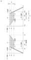
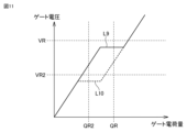
図2は、スイッチング素子1のターンオン動作時における、スイッチング素子1のゲート電荷量とゲート電圧との関係(左側)、および、コンデンサ電圧とスイッチング素子1のゲート電圧との関係(右側)を示す図である。ゲート電荷量とゲート電圧との関係を示す左側の図において、スイッチング素子1の通常時(非短絡時)の関係が破線L1で表わされ、スイッチング素子1のアーム短絡時の関係が実線L2で表わされる。また、コンデンサ電圧とゲート電圧との関係を示す右側の図において、スイッチング素子1の通常時の関係が破線L3で表わされ、スイッチング素子1のアーム短絡時の関係が実線L4で表わされる。
上記の関係式(2)において、「Ci」はスイッチング素子1の入力容量(ゲートソース間容量とゲートドレイン間容量とを合計した全体の容量)を表わし、「Vc」はコンデンサ充電電圧(コンデンサ電圧の初期値)を表わす。なお、負バイアス電位Voff、駆動電圧Von、コンデンサ4の容量Cbは、上述したとおりである。
図4は、本実施の形態2による駆動装置100Aを有する半導体装置DAの一例を示す図である。図4に示す駆動装置100Aは、上述の図1に示す駆動装置100に対して、負バイアス電位Voffを出力する電圧源9を削除するとともに、スイッチング素子6をオフ抵抗20に置き換えたものである。駆動装置100Aのその他の構成は、上述の駆動装置100の構成と同じであるため、ここでの詳細な説明は繰返さない。
上述の実施の形態1では、スイッチング素子1のゲート電荷量とゲート電圧との関係(図2参照)を利用してスイッチング素子1の短絡判定を行なう例について説明した。
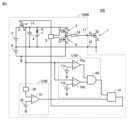
図7は、本実施の形態4による駆動装置100Cを有する半導体装置DCの一例を示す図である。図7に示す駆動装置100Cは、上述の図1に示す駆動装置100に対して、比較部10,12の入力部分にそれぞれフィルタ40,41を追加したものである。駆動装置100Cのその他の構成は、上述の駆動装置100の構成と同じであるため、ここでの詳細な説明は繰返さない。
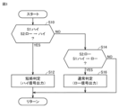
上述の実施の形態1~4では、いずれにおいてもミラー期間の有無を判定することによって、スイッチング素子1の短絡状態を検出する。
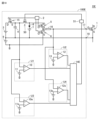
図10は、本実施の形態6による駆動装置100Eを有する半導体装置DEの一例を示す図である。図10に示す駆動装置100Eは、上述の図8に示す駆動装置100Dに対して、第3比較装置U3および第4比較装置U4を追加し、短絡判定器14を短絡判定器14Eに変更したものである。駆動装置100Eのその他の構成は、上述の駆動装置100Dの構成と同じであるため、ここでの詳細な説明は繰返さない。
本実施の形態7は、上述した実施の形態1~6による半導体装置D~DEのいずれかを電力変換装置に適用したものである。以下、実施の形態7として、三相のインバータに本開示を適用した場合について説明する。
Claims (10)
- ゲート端子を有する電力用の半導体素子の駆動装置であって、
第1電圧源と、
スイッチング素子と、
前記スイッチング素子を介して前記第1電圧源と並列に接続されるコンデンサと、
前記コンデンサと前記半導体素子の前記ゲート端子との間に設けられ、前記ゲート端子に印加される電圧を切替可能に構成される切替装置と、
前記コンデンサの電圧と第1基準値との比較結果を示す信号を出力する第1比較装置と、
前記ゲート端子の電圧または前記コンデンサの電圧を微分した値と第2基準値との比較結果を示す信号を出力する第2比較装置と、
前記第1比較装置の出力信号と前記第2比較装置の出力信号とを用いて前記半導体素子が短絡状態であるか否かを判定する判定器と、
を備える、半導体素子の駆動装置。 - 前記第1比較装置は、
前記コンデンサの電圧が前記第1基準値以下である場合にロー状態を示す信号を出力し、
前記コンデンサの電圧が前記第1基準値よりも大きい場合にハイ状態を示す信号を出力し、
前記第2比較装置は、
前記ゲート端子の電圧または前記コンデンサの電圧を微分した値が前記第2基準値以下である場合にロー状態を示す信号を出力し、
前記ゲート端子の電圧または前記コンデンサの電圧を微分した値が前記第2基準値よりも大きい場合にハイ状態を示す信号を出力し、
前記判定器は、
前記第1比較装置の出力信号が前記ハイ状態である時に前記第2比較装置の出力信号が前記ロー状態から前記ハイ状態に変化した場合、前記半導体素子が短絡状態であると判定し、
前記第2比較装置の出力信号が前記ロー状態である時に前記第1比較装置の出力信号が前記ハイ状態から前記ロー状態に変化した場合、前記半導体素子が短絡状態ではないと判定する、請求項1に記載の半導体素子の駆動装置。 - 前記第1電圧源と直列に接続される第2電圧源をさらに備え、
前記切替装置は、前記第1電圧源および前記第2電圧源と並列に接続され、前記ゲート端子に印加される電圧を、前記第1電圧源または前記コンデンサからの正電圧と、前記第2電圧源からの負電圧との間で切替可能に構成される、請求項1または2に記載の半導体素子の駆動装置。 - 前記半導体素子に接続可能な出力端子と、
前記コンデンサと前記出力端子との間に設けられ、前記判定器の出力に応じて前記コンデンサと前記出力端子を切り離すように動作する切り離し装置と、
前記切り離し装置およびダイオードを介して前記コンデンサと並列に接続されるとともに前記ダイオードを介して前記出力端子に接続され、前記コンデンサの電圧よりも低い電圧を出力する安定化用の電圧源と、
をさらに備える、請求項1~3のいずれか1項に記載の半導体素子の駆動装置。 - 前記コンデンサの電圧と、前記第1基準値とは異なる基準値との比較結果を示す信号を出力する第3比較装置と、
前記ゲート端子の電圧または前記コンデンサの電圧を微分した値と、前記第2基準値とは異なる基準値との比較結果を示す信号を出力する第4比較装置とをさらに備え、
前記判定器は、前記第1比較装置の出力信号、前記第2比較装置の出力信号、前記第3比較装置の出力信号、および前記第4比較装置の出力信号を用いて前記半導体素子のミラー期間を検出し、
前記切り離し装置は、前記判定器によって前記ミラー期間が検出されたことに応じて前記コンデンサと前記出力端子とを切り離すように動作する、請求項4に記載の半導体素子の駆動装置。 - 前記第2比較装置は、
前記コンデンサの電圧の微分値を出力する微分器と、
前記微分器の出力と前記第2基準値とを比較する比較器と、
を備える、請求項1~5のいずれか1項に記載の半導体素子の駆動装置。 - 前記半導体素子をオン状態にするときの前記ゲート端子の電圧をVon、前記半導体素子をオフ状態にするときの前記ゲート端子の電圧をVoff、前記半導体素子の入力容量をCi、前記コンデンサの充電電圧をVc、前記コンデンサの容量をCbと記載するとき、
前記コンデンサの容量Cbが、
Cb≦{|Voff-Von|/|Vc-Von|×Ci}
の関係式を満たす、請求項1~6のいずれか1項に記載の半導体素子の駆動装置。 - 前記半導体素子は、シリコン、シリコンカーバイド、ガリウムナイトライド、および酸化ガリウムのいずれかを材料とする素子である、請求項1~7のいずれか1項に記載の半導体素子の駆動装置。
- 請求項1~8のいずれか1項に記載の駆動装置および半導体素子を備える、半導体装置。
- 請求項1~8のいずれか1項に記載の駆動装置および半導体素子を有し、入力される電力を変換して出力する主変換回路と、
前記主変換回路を制御する制御信号を前記主変換回路に出力する制御回路と、
を備えた電力変換装置。
Applications Claiming Priority (1)
| Application Number | Priority Date | Filing Date | Title |
|---|---|---|---|
| PCT/JP2020/033793 WO2022049772A1 (ja) | 2020-09-07 | 2020-09-07 | 半導体素子の駆動装置、半導体装置および電力変換装置 |
Publications (2)
| Publication Number | Publication Date |
|---|---|
| JPWO2022049772A1 JPWO2022049772A1 (ja) | 2022-03-10 |
| JP7523552B2 true JP7523552B2 (ja) | 2024-07-26 |
Family
ID=80490893
Family Applications (1)
| Application Number | Title | Priority Date | Filing Date |
|---|---|---|---|
| JP2022546858A Active JP7523552B2 (ja) | 2020-09-07 | 2020-09-07 | 半導体素子の駆動装置、半導体装置および電力変換装置 |
Country Status (5)
| Country | Link |
|---|---|
| US (1) | US12206401B2 (ja) |
| JP (1) | JP7523552B2 (ja) |
| CN (1) | CN116491039B (ja) |
| DE (1) | DE112020007591T5 (ja) |
| WO (1) | WO2022049772A1 (ja) |
Families Citing this family (3)
| Publication number | Priority date | Publication date | Assignee | Title |
|---|---|---|---|---|
| CN117378144A (zh) * | 2021-05-25 | 2024-01-09 | 三菱电机株式会社 | 半导体元件的驱动方法和驱动装置以及电力变换装置 |
| US12609227B2 (en) * | 2022-12-20 | 2026-04-21 | Metamagnetics, Inc. | Temperature stable magnetostatic wave RF devices and related techniques |
| KR102860088B1 (ko) * | 2023-08-17 | 2025-09-15 | 한화솔루션 주식회사 | 전력변환장치 및 그 제어 방법 |
Citations (3)
| Publication number | Priority date | Publication date | Assignee | Title |
|---|---|---|---|---|
| JP2015053749A (ja) | 2013-09-05 | 2015-03-19 | 三菱電機株式会社 | 電力用半導体素子の駆動回路 |
| JP2018098938A (ja) | 2016-12-14 | 2018-06-21 | 三菱電機株式会社 | 駆動システムおよび電力変換装置 |
| WO2019021590A1 (ja) | 2017-07-28 | 2019-01-31 | 三菱電機株式会社 | 電力用半導体素子の駆動回路 |
Family Cites Families (11)
| Publication number | Priority date | Publication date | Assignee | Title |
|---|---|---|---|---|
| EP0354435B1 (en) * | 1988-08-12 | 1995-12-20 | Hitachi, Ltd. | A drive circuit for an insulated gate transistor; and its use in a switching circuit, a current switching apparatus and an induction motor system |
| JP4223331B2 (ja) * | 2003-06-13 | 2009-02-12 | 株式会社日立製作所 | 電力制御用半導体素子の保護装置及びそれを備えた電力変換装置 |
| JP4804142B2 (ja) | 2005-12-21 | 2011-11-02 | 東洋電機製造株式会社 | 高速ゲート駆動回路 |
| JP2009225506A (ja) * | 2008-03-13 | 2009-10-01 | Toshiba Corp | 電力変換器 |
| CN102160271B (zh) * | 2008-09-22 | 2013-11-20 | 富士通株式会社 | 电源控制电路、电源装置以及电源控制装置的控制方法 |
| JP6300964B1 (ja) * | 2017-01-13 | 2018-03-28 | 三菱電機株式会社 | 電力変換装置 |
| JP6264491B1 (ja) * | 2017-05-11 | 2018-01-24 | 富士電機株式会社 | 短絡検出装置および装置 |
| US11050418B2 (en) * | 2019-01-11 | 2021-06-29 | Infineon Technologies Ag | Gate level triggered desaturation blanking |
| US11519954B2 (en) * | 2019-08-27 | 2022-12-06 | Analog Devices International Unlimited Company | Apparatus and method to achieve fast-fault detection on power semiconductor devices |
| JP7530385B2 (ja) * | 2019-12-12 | 2024-08-07 | ローム株式会社 | スイッチング回路のゲート駆動回路およびスイッチング電源の制御回路 |
| WO2022265597A1 (en) * | 2021-06-14 | 2022-12-22 | Istanbul Teknik Universitesi | A short circuit protection system for battery packs |
-
2020
- 2020-09-07 WO PCT/JP2020/033793 patent/WO2022049772A1/ja not_active Ceased
- 2020-09-07 DE DE112020007591.5T patent/DE112020007591T5/de active Pending
- 2020-09-07 JP JP2022546858A patent/JP7523552B2/ja active Active
- 2020-09-07 CN CN202080103745.4A patent/CN116491039B/zh active Active
- 2020-09-07 US US18/015,720 patent/US12206401B2/en active Active
Patent Citations (3)
| Publication number | Priority date | Publication date | Assignee | Title |
|---|---|---|---|---|
| JP2015053749A (ja) | 2013-09-05 | 2015-03-19 | 三菱電機株式会社 | 電力用半導体素子の駆動回路 |
| JP2018098938A (ja) | 2016-12-14 | 2018-06-21 | 三菱電機株式会社 | 駆動システムおよび電力変換装置 |
| WO2019021590A1 (ja) | 2017-07-28 | 2019-01-31 | 三菱電機株式会社 | 電力用半導体素子の駆動回路 |
Also Published As
| Publication number | Publication date |
|---|---|
| CN116491039B (zh) | 2025-06-27 |
| CN116491039A (zh) | 2023-07-25 |
| JPWO2022049772A1 (ja) | 2022-03-10 |
| US12206401B2 (en) | 2025-01-21 |
| DE112020007591T5 (de) | 2023-06-22 |
| WO2022049772A1 (ja) | 2022-03-10 |
| US20230261654A1 (en) | 2023-08-17 |
Similar Documents
| Publication | Publication Date | Title |
|---|---|---|
| US10038438B2 (en) | Power semiconductor element driving circuit | |
| US7777437B2 (en) | Switching control system and motor driving system | |
| JP7523552B2 (ja) | 半導体素子の駆動装置、半導体装置および電力変換装置 | |
| JP2018182818A (ja) | スイッチング素子駆動装置 | |
| JP6988670B2 (ja) | 駆動回路、パワーモジュール及び電力変換システム | |
| CN105896940B (zh) | 电力转换装置 | |
| US11728802B2 (en) | Drive circuit | |
| JP7471426B2 (ja) | 電力用半導体素子の駆動制御回路、電力用半導体モジュール、および電力変換装置 | |
| CN111971884A (zh) | 栅极驱动电路和栅极驱动方法 | |
| JPH0923664A (ja) | インバータ装置 | |
| CN110911229A (zh) | 具有保护功能的感性线圈驱动电路 | |
| US11404953B2 (en) | Drive circuit for power semiconductor element and power semiconductor module employing the same | |
| CN115694447B (zh) | 用于双向开关的短路保护 | |
| CN112039505A (zh) | 用于运行电路的方法、电路以及机动车 | |
| CN115298943A (zh) | 半导体驱动装置、半导体装置以及电力变换装置 | |
| CN113056864B (zh) | 电力转换装置 | |
| JP4151163B2 (ja) | Mosトランジスタのドライブ回路 | |
| US20250364986A1 (en) | Programmable gate voltage for on resistance control of power module | |
| US20240258901A1 (en) | Gate drive circuit and power conversion device | |
| US20250226815A1 (en) | Drive circuit and control method for drive circuit | |
| US20250364984A1 (en) | Programmable gate voltage for on resistance control of power module | |
| US20250274056A1 (en) | Method of operating an inverter circuit, inverter arrangement and drive unit | |
| WO2023157185A1 (ja) | ゲート駆動回路及び電力変換装置 | |
| CN118353337A (zh) | 具有相位转换速率控制和过流保护的栅极驱动 | |
| CN116470895A (zh) | 固态接触器的组件和三相固态接触器 |
Legal Events
| Date | Code | Title | Description |
|---|---|---|---|
| A621 | Written request for application examination |
Free format text: JAPANESE INTERMEDIATE CODE: A621 Effective date: 20230202 |
|
| A131 | Notification of reasons for refusal |
Free format text: JAPANESE INTERMEDIATE CODE: A131 Effective date: 20240227 |
|
| A521 | Request for written amendment filed |
Free format text: JAPANESE INTERMEDIATE CODE: A523 Effective date: 20240410 |
|
| TRDD | Decision of grant or rejection written | ||
| A01 | Written decision to grant a patent or to grant a registration (utility model) |
Free format text: JAPANESE INTERMEDIATE CODE: A01 Effective date: 20240618 |
|
| A61 | First payment of annual fees (during grant procedure) |
Free format text: JAPANESE INTERMEDIATE CODE: A61 Effective date: 20240716 |
|
| R150 | Certificate of patent or registration of utility model |
Ref document number: 7523552 Country of ref document: JP Free format text: JAPANESE INTERMEDIATE CODE: R150 |