JP7523552B2 - Semiconductor element driving device, semiconductor device, and power conversion device - Google Patents
Semiconductor element driving device, semiconductor device, and power conversion device Download PDFInfo
- Publication number
- JP7523552B2 JP7523552B2 JP2022546858A JP2022546858A JP7523552B2 JP 7523552 B2 JP7523552 B2 JP 7523552B2 JP 2022546858 A JP2022546858 A JP 2022546858A JP 2022546858 A JP2022546858 A JP 2022546858A JP 7523552 B2 JP7523552 B2 JP 7523552B2
- Authority
- JP
- Japan
- Prior art keywords
- voltage
- capacitor
- semiconductor element
- switching element
- reference value
- Prior art date
- Legal status (The legal status is an assumption and is not a legal conclusion. Google has not performed a legal analysis and makes no representation as to the accuracy of the status listed.)
- Active
Links
Images


Classifications
-
- H—ELECTRICITY
- H02—GENERATION; CONVERSION OR DISTRIBUTION OF ELECTRIC POWER
- H02M—APPARATUS FOR CONVERSION BETWEEN AC AND AC, BETWEEN AC AND DC, OR BETWEEN DC AND DC, AND FOR USE WITH MAINS OR SIMILAR POWER SUPPLY SYSTEMS; CONVERSION OF DC OR AC INPUT POWER INTO SURGE OUTPUT POWER; CONTROL OR REGULATION THEREOF
- H02M1/00—Details of apparatus for conversion
- H02M1/08—Circuits specially adapted for the generation of control voltages for semiconductor devices incorporated in static converters
-
- H—ELECTRICITY
- H03—ELECTRONIC CIRCUITRY
- H03K—PULSE TECHNIQUE
- H03K17/00—Electronic switching or gating, i.e. not by contact-making and –breaking
- H03K17/51—Electronic switching or gating, i.e. not by contact-making and –breaking characterised by the components used
- H03K17/56—Electronic switching or gating, i.e. not by contact-making and –breaking characterised by the components used by the use, as active elements, of semiconductor devices
- H03K17/687—Electronic switching or gating, i.e. not by contact-making and –breaking characterised by the components used by the use, as active elements, of semiconductor devices the devices being field-effect transistors
- H03K17/6871—Electronic switching or gating, i.e. not by contact-making and –breaking characterised by the components used by the use, as active elements, of semiconductor devices the devices being field-effect transistors the output circuit comprising more than one controlled field-effect transistor
-
- H—ELECTRICITY
- H03—ELECTRONIC CIRCUITRY
- H03K—PULSE TECHNIQUE
- H03K17/00—Electronic switching or gating, i.e. not by contact-making and –breaking
- H03K17/06—Modifications for ensuring a fully conducting state
- H03K17/063—Modifications for ensuring a fully conducting state in field-effect transistor switches
-
- H—ELECTRICITY
- H03—ELECTRONIC CIRCUITRY
- H03K—PULSE TECHNIQUE
- H03K17/00—Electronic switching or gating, i.e. not by contact-making and –breaking
- H03K17/08—Modifications for protecting switching circuit against overcurrent or overvoltage
- H03K17/081—Modifications for protecting switching circuit against overcurrent or overvoltage without feedback from the output circuit to the control circuit
- H03K17/0812—Modifications for protecting switching circuit against overcurrent or overvoltage without feedback from the output circuit to the control circuit by measures taken in the control circuit
- H03K17/08122—Modifications for protecting switching circuit against overcurrent or overvoltage without feedback from the output circuit to the control circuit by measures taken in the control circuit in field-effect transistor switches
-
- H—ELECTRICITY
- H02—GENERATION; CONVERSION OR DISTRIBUTION OF ELECTRIC POWER
- H02H—EMERGENCY PROTECTIVE CIRCUIT ARRANGEMENTS
- H02H7/00—Emergency protective circuit arrangements specially adapted for specific types of electric machines or apparatus or for sectionalised protection of cable or line systems, and effecting automatic switching in the event of an undesired change from normal working conditions
- H02H7/10—Emergency protective circuit arrangements specially adapted for specific types of electric machines or apparatus or for sectionalised protection of cable or line systems, and effecting automatic switching in the event of an undesired change from normal working conditions for converters; for rectifiers
- H02H7/12—Emergency protective circuit arrangements specially adapted for specific types of electric machines or apparatus or for sectionalised protection of cable or line systems, and effecting automatic switching in the event of an undesired change from normal working conditions for converters; for rectifiers for static converters or rectifiers
- H02H7/122—Emergency protective circuit arrangements specially adapted for specific types of electric machines or apparatus or for sectionalised protection of cable or line systems, and effecting automatic switching in the event of an undesired change from normal working conditions for converters; for rectifiers for static converters or rectifiers for inverters, i.e. DC/AC converters
- H02H7/1225—Emergency protective circuit arrangements specially adapted for specific types of electric machines or apparatus or for sectionalised protection of cable or line systems, and effecting automatic switching in the event of an undesired change from normal working conditions for converters; for rectifiers for static converters or rectifiers for inverters, i.e. DC/AC converters responsive to internal faults, e.g. shoot-through
Landscapes
- Engineering & Computer Science (AREA)
- Power Engineering (AREA)
- Power Conversion In General (AREA)
- Protection Of Static Devices (AREA)
Description
本開示は、半導体素子の駆動装置、および、その半導体素子と駆動装置とを有する半導体装置ならびに電力変換装置に関する。 The present disclosure relates to a driving device for a semiconductor element, and a semiconductor device and a power conversion device having the semiconductor element and the driving device.
電力変換器を構成する電力用の半導体素子にはSi(シリコン)を材料とするIGBT(Insulated Gate Bipolar Transistor)がよく用いられるが、最近では電力変換器の更なる小型化、高効率化を実現するためにSiC(シリコンカーバイト)を材料とするMOSFET(Metal Oxide Semiconductor Field Effect Transistor)の適用が盛んになってきている。 IGBTs (Insulated Gate Bipolar Transistors) made of Si (silicon) are often used as the power semiconductor elements that make up power converters, but recently the use of MOSFETs (Metal Oxide Semiconductor Field Effect Transistors) made of SiC (silicon carbide) has become more common in order to further reduce the size and improve the efficiency of power converters.
電力変換器において電力用の半導体素子が短絡状態になると、電力変換器の直流リンク電圧が電力用の半導体素子に印加された状態で大電流が流れることになり、非常に大きな損失(熱)が発生する可能性がある。そのため、電力変換器の信頼性を確保するためには、電力用の半導体素子の短絡状態を検出する回路を設けることが望ましい。 When a power semiconductor element in a power converter is short-circuited, a large current flows with the DC link voltage of the power converter applied to the power semiconductor element, which can result in very large losses (heat). Therefore, in order to ensure the reliability of the power converter, it is desirable to provide a circuit that detects the short-circuit state of the power semiconductor element.
電力用の半導体素子の短絡状態を高速に検出する手段として、従来の電力用の半導体素子の駆動装置のなかには、電力用の半導体素子のゲートに供給されるゲート電荷量を検出する装置と、電力用の半導体素子のゲート電圧を検出する装置とを備える駆動装置がある(例えば特許文献1)。As a means for quickly detecting a short circuit state in a power semiconductor element, among conventional power semiconductor element driving devices, there is a driving device that includes a device for detecting the amount of gate charge supplied to the gate of the power semiconductor element, and a device for detecting the gate voltage of the power semiconductor element (for example, Patent Document 1).
特開2015-53749号公報(特許文献1)に記載の駆動装置は、ゲート電荷量とゲート電圧との関係が短絡時と通常時とで異なることを利用して短絡状態を検出するために、ゲート電荷量を検出する検出装置が必要になる。この検出装置は、電流センサの出力およびゲート抵抗の両端電圧をモニタすることでゲート電流を検出し、検出されたゲート電流を積分することによってゲート電荷量を検出する。そのため、積分器が必要となり、回路規模が大きくなってしまうという課題があった。The driving device described in JP 2015-53749 A (Patent Document 1) requires a detection device to detect the gate charge amount in order to detect a short circuit state by utilizing the fact that the relationship between the gate charge amount and the gate voltage differs between a short circuit and normal operation. This detection device detects the gate current by monitoring the output of the current sensor and the voltage across the gate resistor, and detects the gate charge amount by integrating the detected gate current. This necessitates an integrator, which poses the problem of a large circuit size.
本開示は、上述の課題を解決するためになされたものであって、その目的は、積分器を使用することなく簡素な回路で電力用の半導体素子の短絡判定を行なうことを可能にすることである。 The present disclosure has been made to solve the above-mentioned problems, and its purpose is to make it possible to determine whether a power semiconductor element is short-circuited using a simple circuit without using an integrator.
本開示による駆動装置は、ゲート端子を有する電力用の半導体素子の駆動装置であって、第1電圧源と、スイッチング素子と、スイッチング素子を介して第1電圧源と並列に接続されるコンデンサと、コンデンサと半導体素子のゲート端子との間に設けられ、ゲート端子に印加される電圧を切替可能に構成される切替装置と、コンデンサの電圧と第1基準値との比較結果を示す信号を出力する第1比較装置と、ゲート端子の電圧または電圧微分値と第2基準値との比較結果を示す信号を出力する第2比較装置と、第1比較装置の出力信号と第2比較装置の出力信号とを用いて半導体素子が短絡状態であるか否かを判定する判定器と、を備える。The driving device according to the present disclosure is a driving device for a power semiconductor element having a gate terminal, and includes a first voltage source, a switching element, a capacitor connected in parallel to the first voltage source via the switching element, a switching device provided between the capacitor and the gate terminal of the semiconductor element and configured to be able to switch the voltage applied to the gate terminal, a first comparison device that outputs a signal indicating the comparison result between the capacitor voltage and a first reference value, a second comparison device that outputs a signal indicating the comparison result between the gate terminal voltage or a voltage differential value and a second reference value, and a determiner that determines whether the semiconductor element is in a short-circuit state using the output signal of the first comparison device and the output signal of the second comparison device.
上記の駆動装置においては、ゲート電荷量を直接的に検出した結果で半導体素子の短絡判定を行なうのではなく、コンデンサの電圧とスイッチング素子のゲート電圧またはその微分値とをモニタすることによって、半導体素子の短絡判定を行なう。そのため、ゲート電荷量を検出するための積分器を使用することなく、簡素な回路で半導体素子の短絡判定を行なうことができる。In the above drive device, the short circuit of the semiconductor element is judged not by directly detecting the gate charge amount, but by monitoring the capacitor voltage and the gate voltage of the switching element or its differential value. Therefore, it is possible to judge the short circuit of the semiconductor element with a simple circuit without using an integrator to detect the gate charge amount.
本開示によれば、積分器を使用することなく簡素な回路で電力用の半導体素子の短絡判定を行なうことができる。 According to the present disclosure, it is possible to determine whether a power semiconductor element is short-circuited using a simple circuit without using an integrator.
以下、本開示の実施の形態について、図面を参照しながら詳細に説明する。なお、図中同一または相当部分には同一符号を付してその説明は繰返さない。Hereinafter, the embodiments of the present disclosure will be described in detail with reference to the drawings. Note that the same or corresponding parts in the drawings are designated by the same reference numerals and their description will not be repeated.
実施の形態1.
図1は、本実施の形態1による駆動装置100を有する半導体装置Dの一例を示す図である。半導体装置Dは、電力用の半導体素子であるスイッチング素子1と、スイッチング素子1を駆動するための駆動装置100とを備える。
1 is a diagram showing an example of a semiconductor device D having a
本実施の形態1においては、スイッチング素子1がMOSFETである場合について説明する。一般的に、MOSFETは、ゲート電圧(ゲートソース間電圧)がしきい電圧未満である場合にドレイン電流(ソースとドレインとの間を流れる電流)が生じないオフ状態(遮断状態)となり、ゲート電圧がしきい電圧以上である場合にドレイン電流が生じるオン状態(導通状態)となるように構成される。In this
以下に説明するスイッチング素子5,6,15,50についても、スイッチング素子1と同様に、MOSFETである場合について説明する。なお、スイッチング素子1およびスイッチング素子5,6,15,50は、MOSFETに限定されるものではなく、例えば、IGBT等の電圧駆動型の半導体素子であってもよい。また、IGBTは、逆導通IGBT(RC-IGBT)であってもよい。
The
また、スイッチング素子1,5,6,15は、Si(シリコン)、SiC(シリコンカーバイド)、GaN(ガリウムナイトライド)、およびGa2O3(酸化ガリウム)のいずれかを材料としたデバイスに適用可能である。
Moreover, the
駆動装置100は、指令部2と、電圧源3,7,9と、コンデンサ4と、スイッチング素子5,6,15と、ダイオード8と、一対の出力端子17,18と、第1比較装置U1と、第2比較装置U2と、短絡判定器14と、ゲート抵抗16と、を備える。第1比較装置U1は、比較部10と電圧源11とを備える。第2比較装置U2は、比較部12と電圧源13とを備える。The
出力端子17,18は、スイッチング素子1のゲートおよびソースにそれぞれ接続される。
電圧源3は、スイッチング素子15を介してコンデンサ4に接続される。具体的には、電圧源3の正極はスイッチング素子15を介してコンデンサ4の一方端に接続され、電圧源3の負極はコンデンサ4の他方端に接続される。The
電圧源9は、電圧源3と直列に接続される。電圧源9の正極は電圧源3の負極および出力端子18に接続され、電圧源9の負極はスイッチング素子6のドレイン端子に接続される。The voltage source 9 is connected in series with the
コンデンサ4は、スイッチング素子15を介して電圧源3と並列に接続される。
電圧源7は、ダイオード8を介してコンデンサ4の一方端に接続され、コンデンサ4の一方端に駆動電圧Vonを供給する。電圧源7およびダイオード8によって、スイッチング素子1の定常オン状態の電圧が駆動電圧Vonに安定する。
The
The
スイッチング素子5は、N型のMOSFETである。スイッチング素子5のソース端子は、ゲート抵抗16を介して駆動装置100の出力端子17に接続される。ゲート抵抗16は、スイッチング素子5のスイッチング速度を調節するための抵抗である。スイッチング素子5のドレイン端子は、コンデンサ4の一方端に接続されるとともに、スイッチング素子15を介して電圧源3の正極に接続される。The
スイッチング素子5のゲート端子は、指令部2に接続され、指令部2からのゲート電圧を受ける。スイッチング素子5のゲート端子に指令部2からのゲート電圧が印加されると、スイッチング素子5はオン状態となり、コンデンサ4の一方端と出力端子17とが接続される。これにより、駆動装置100の出力電圧は、コンデンサ4の電圧(コンデンサ4の端子間電圧、以下、単に「コンデンサ電圧」ともいう)となる。
The gate terminal of the
スイッチング素子6は、スイッチング素子5と同様、N型のMOSFETである。スイッチング素子6のドレイン端子は、ゲート抵抗16を介して駆動装置100の出力端子17に接続される。スイッチング素子6のソース端子は、電圧源9の負極に接続される。The
スイッチング素子6のゲート端子は、指令部2に接続され、指令部2からのゲート電圧を受ける。スイッチング素子6のゲート端子に指令部2からのゲート電圧が印加されると、スイッチング素子6はオン状態となり、電圧源9の負極と出力端子17とが接続される。これにより、出力電圧は、電圧源9により供される負バイアス電位Voffとなる。The gate terminal of the
スイッチング素子5,6は、指令部2により、互いに相補的に動作するように制御される。すなわち、スイッチング素子5がオン状態である場合にスイッチング素子6はオフ状態となり、スイッチング素子5がオフ状態である場合にスイッチング素子6はオン状態となる。これにより、スイッチング素子1の定常オン時にスイッチング素子1のゲート端子に駆動電圧Vonを印加し、スイッチング素子1の定常オフ時にスイッチング素子1のゲート端子に負バイアス電位Voffを印加することができる。
The
指令部2は、外部より入力されるゲート信号に基づいて予め指定されたタイミングでスイッチング素子5,6,15にゲート電圧をそれぞれ与えることによって、スイッチング素子5,6,15のオンオフを制御する。指令部2は、スイッチング素子5のオンオフと、スイッチング素子6のオンオフと、スイッチング素子15のオンオフとを、それぞれ別々に制御可能に構成される。The
スイッチング素子1は、指令部2からの信号に基づいて、オン状態、オフ状態を遷移する。
The
スイッチング素子1をオフ状態にする場合、指令部2は、スイッチング素子15をオン状態にし、スイッチング素子5をオフ状態にし、スイッチング素子6をオン状態にするためのオフ指令を各スイッチング素子5,6,15に出力する。スイッチング素子15がオン状態とされることにより、コンデンサ4が電圧源3にて充電されてコンデンサ電圧が電圧源3の出力電圧となる。これにより、スイッチング素子1のスイッチングに必要な電荷量がコンデンサ4に蓄えられる。また、スイッチング素子5がオフ状態、スイッチング素子6がオン状態とされることより、スイッチング素子1のゲート端子には、電圧源9からの負バイアス電位Voffが印加される。
When switching
スイッチング素子1をオフ状態からオン状態に変化させる場合、指令部2は、まずスイッチング素子15をオン状態からオフ状態に変化させることによって、コンデンサ4を電圧源3から切り離す。When changing the
その後、指令部2は、スイッチング素子5をオン状態、スイッチング素子6をオフ状態にそれぞれ切り替える。これにより、スイッチング素子1のゲート端子は、ゲート抵抗16を介してコンデンサ4に接続される。コンデンサ4に充電された電荷はスイッチング素子1のゲートへ流入する。スイッチング素子1のゲート電圧が上昇するにつれて、コンデンサ4の電圧は低下する。このとき、コンデンサ電圧の初期値(電圧源3の出力電圧)を駆動電圧Von(電圧源7の出力電圧)よりも高い電圧に設定することにより、駆動電圧Vonにて定電圧駆動をした場合と比較し、スイッチング素子1を高速でスイッチングすることが可能となる。
After that, the
コンデンサ電圧が初期値から駆動電圧Vonまで低下すると、ダイオード8が導通し、出力電圧は駆動電圧Vonで一定となる。このとき、駆動装置100からスイッチング素子1のゲートへ流入した電荷量(以下「ゲート電荷量」ともいう)は、コンデンサ4が放出した電荷量に等しい。そのため、ゲート電荷量を「Qg」、コンデンサ4の容量を「Cb」、コンデンサ電圧の減少幅を「ΔV」と記載するとき、これらの間には、下記の関係式(1)が成立する。When the capacitor voltage drops from its initial value to the drive voltage Von, the
ΔV×Cb=Qg …(1)
上記の関係式(1)において、コンデンサ4の容量Cbは予め決められた値であるため、コンデンサ電圧を検出してコンデンサ電圧の減少幅ΔVを求めることによって、ゲート電荷量Qgを検出することができる。そのため、ゲート電荷量Qgを検出するにあたり、積分回路等の演算回路が不要であり、コンデンサ電圧からゲート電荷量Qgを直接的に検出することができる。そのため、回路規模を小さくすることができる。
ΔV×Cb=Qg…(1)
In the above relational expression (1), since the capacitance Cb of the
第1比較装置U1は、上記の関係式(1)を利用して、コンデンサ電圧からゲート電荷量Qgを検出する。具体的には、第1比較装置U1は、上述したように、比較部10と、電圧源11とを備える。電圧源11は基準値VQRの電圧を比較部10に出力する。The first comparison device U1 detects the gate charge Qg from the capacitor voltage using the above relational expression (1). Specifically, as described above, the first comparison device U1 includes a
比較部10は、コンデンサ電圧を電圧源11が出力する基準値VQRの電圧と比較してコンデンサ電圧が基準値VQRに低下したことを検出することで、ゲート電荷量Qgが基準値QRに達したことを検出する。The
比較部10は、コンデンサ電圧と基準値VQRとの比較結果を示す出力信号S1を短絡判定器14に出力する。比較部10は、コンデンサ電圧が基準値VQR以下である場合には出力信号S1をロー状態にし、コンデンサ電圧が基準値VQRよりも大きい場合には出力信号S1をハイ状態にする。The
また、第2比較装置U2は、上述したように、比較部12と、電圧源13とを備える。電圧源13は、基準値VRの電圧を比較部12に出力する。比較部12は、スイッチング素子1のゲート電圧(駆動装置100からスイッチング素子1のゲート端子に印加される電圧)と、電圧源13が出力する基準値VRの電圧とを比較することにより、スイッチング素子1のゲート電圧が基準値VRに達したことを検出する。As described above, the second comparison device U2 includes a
比較部12は、スイッチング素子1のゲート電圧と基準値VRとの比較結果を示す出力信号S2を短絡判定器14に出力する。比較部12は、スイッチング素子1のゲート電圧が基準値VR以下である場合には出力信号S2をロー状態とし、スイッチング素子1のゲート電圧が基準値VRよりも大きい場合には出力信号S2をハイ状態とする。The
短絡判定器14は、第1比較装置U1の出力信号S1と第2比較装置U2の出力信号S2とを用いて、スイッチング素子1の短絡状態を検出する。The short-
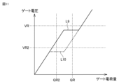
[スイッチング素子1の短絡判定]
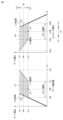
図2は、スイッチング素子1のターンオン動作時における、スイッチング素子1のゲート電荷量とゲート電圧との関係(左側)、および、コンデンサ電圧とスイッチング素子1のゲート電圧との関係(右側)を示す図である。ゲート電荷量とゲート電圧との関係を示す左側の図において、スイッチング素子1の通常時(非短絡時)の関係が破線L1で表わされ、スイッチング素子1のアーム短絡時の関係が実線L2で表わされる。また、コンデンサ電圧とゲート電圧との関係を示す右側の図において、スイッチング素子1の通常時の関係が破線L3で表わされ、スイッチング素子1のアーム短絡時の関係が実線L4で表わされる。
[Determination of short circuit of switching element 1]
2 is a diagram showing the relationship between the gate charge and gate voltage of the switching element 1 (left side) and the relationship between the capacitor voltage and the gate voltage of the switching element 1 (right side) during the turn-on operation of the
なお、図2においては、スイッチング素子1が、SiC(シリコンカーバイド)を材料としたMOSFET(以下「SiC-MOSFET」ともいう)である場合の関係を例示している。
Note that Figure 2 illustrates an example of the relationship when the switching
スイッチング素子1の通常時においては、ゲート電圧が上昇すると、ゲート電荷量は増加し、コンデンサ電圧は減少する。ゲート電圧が電圧Vmにまで上昇すると、ゲート電圧の上昇率は大幅に低下する。ゲート電圧が電圧Vmに達したとき、ゲート電荷量は電荷量Q0であり、コンデンサ電圧は電圧VQ0(VQ0=Q0/Cb)である。なお、「Cb」は上述したようにコンデンサ4の容量である。
Under normal operating conditions of the
その後、ゲート電荷量が電荷量Q1(Q1>Q0)に到達すると、コンデンサ電圧は電圧VQ1(VQ1=Q1/Cb)となる。ゲート電荷量が電荷量Q0から電荷量Q1に達するまでの期間は、ゲート電圧の上昇がごく緩やかとなり、ゲート電圧はほぼ電圧Vmのまま維持される。ゲート電荷量が電荷量Q0から電荷量Q1に達するまでの期間は「ミラー期間」と呼ばれる。 After that, when the gate charge reaches charge Q1 (Q1>Q0), the capacitor voltage becomes voltage VQ1 (VQ1=Q1/Cb). During the period from when the gate charge reaches charge Q1 from charge Q0, the gate voltage increases very slowly and remains at approximately voltage Vm. The period from when the gate charge reaches charge Q1 from charge Q0 is called the "Miller period."
その後、ゲート電荷量が電荷量Q1を超えると、ゲート電圧は再び上昇してゲート駆動電源電圧Vdにまで到達する。これにより、スイッチング素子1がオン状態となる。After that, when the gate charge exceeds the charge Q1, the gate voltage rises again and reaches the gate drive power supply voltage Vd. This causes the
スイッチング素子1のようなSiC-MOSFETにおけるゲート電荷量とゲート電圧との関係においては、帰還容量の存在が大きく寄与している。SiC-MOSFETにおける帰還容量は、ドレイン・ゲート間容量に相当し、大きな電圧依存性を有している。
The presence of feedback capacitance plays a major role in the relationship between the gate charge and gate voltage in a SiC MOSFET such as the switching
スイッチング素子1の通常時におけるターンオン動作時においては、指令部2からの指令に基づきゲート電圧が上昇し、ゲート・ソース間が充電される。ゲート電圧がしきい電圧を超えると、ドレイン電流(ソースとドレインとの間を流れる電流)が流れ始めるとともにドレイン・ソース間電圧は低下し、駆動装置100からスイッチング素子1に供給されるゲート電流は帰還容量を介してスイッチング素子1のゲート端子からドレイン端子に流れる。これにより、ゲート電圧の上昇がごく緩やかなミラー期間が現れる。帰還容量には大きな電圧依存性があり、ドレイン・ソース間電圧がスイッチング素子1のオン電圧まで低下すると帰還容量の値は1桁ないし2桁大きな値となる。その結果、ミラー期間の終了後に、ゲート電圧はゲート駆動電源電圧Vdまで緩やかに上昇する。During normal turn-on operation of the
しかしながら、スイッチング素子1のアーム短絡時においては、このようなミラー期間は現れることなく、スイッチング素子1のゲート電圧はゲート駆動電源電圧Vdまで一気に上昇することになる。However, when the arm of switching
本実施の形態による短絡判定器14は、図2に示した関係を利用して、スイッチング素子1のアーム短絡の有無を判定する。以下、スイッチング素子1のアーム短絡の判定手法について説明する。The
本実施の形態においては、図2の左側に示すゲート電荷量とゲート電圧との関係において、通常時の破線L1とアーム短絡時の実線L2とゲート駆動電源電圧Vdとで囲まれる領域A1内にゲート電荷量の基準値QRおよびゲート電圧の基準値VRが含まれるように、ゲート電荷量の基準値QRおよびゲート電圧の基準値VRが設定される。これを図2の右側に示すコンデンサ電圧とゲート電圧との関係に換算した場合、コンデンサ電圧の基準値VQR(ゲート電荷量が基準値QRであるときのコンデンサ電圧)およびゲート電圧の基準値VRは、通常時の破線L3とアーム短絡時の実線L4とゲート駆動電源電圧Vdとで囲まれる領域A2内に含まれることになる。In this embodiment, in the relationship between the gate charge and gate voltage shown on the left side of Figure 2, the reference value QR of the gate charge and the reference value VR of the gate voltage are set so that they are included in the area A1 surrounded by the dashed line L1 in normal operation, the solid line L2 in arm short-circuiting, and the gate drive power supply voltage Vd. When this is converted into the relationship between the capacitor voltage and gate voltage shown on the right side of Figure 2, the reference value VQR of the capacitor voltage (the capacitor voltage when the gate charge is the reference value QR) and the reference value VR of the gate voltage are included in the area A2 surrounded by the dashed line L3 in normal operation, the solid line L4 in arm short-circuiting, and the gate drive power supply voltage Vd.
スイッチング素子1のスイッチング動作の際、コンデンサ4より流出したゲート電荷量が基準値QRに達すると、コンデンサ電圧は基準値VQRまで低下し、第1比較装置U1の出力信号S1がハイ状態からロー状態に変化する。During the switching operation of the
第1比較装置U1の出力信号S1がハイ状態である時に第2比較装置U2の出力信号S2がロー状態からハイ状態に変化した場合(すなわちコンデンサ電圧が基準値VQRよりも大きい時にゲート電圧が基準値VQRに達した場合)、コンデンサ電圧とゲート電圧との関係はミラー期間のない短絡時の実線L4上の動作点P4で示される(ゲート電荷量とゲート電圧との関係に置き換えるとミラー期間のない短絡時の実線L2上の動作点P2で示される)と考えられるため、短絡判定器14は、スイッチング素子1が短絡状態であると判定し、スイッチング素子1が短絡状態であることを示すハイ信号を指令部2に出力する。
When the output signal S2 of the second comparison device U2 changes from a low state to a high state while the output signal S1 of the first comparison device U1 is in a high state (i.e. when the gate voltage reaches the reference value VQR when the capacitor voltage is greater than the reference value VQR), the relationship between the capacitor voltage and the gate voltage is considered to be shown by the operating point P4 on the solid line L4 when there is a short circuit and no mirror period (when replaced with the relationship between the gate charge and the gate voltage, it is shown by the operating point P2 on the solid line L2 when there is a short circuit and no mirror period), so the short-
一方、第2比較装置U2の出力信号S2がロー状態である時に第1比較装置U1の出力信号S1がハイ状態からロー状態に変化した場合(すなわちゲート電圧が基準値VR以下である時にコンデンサ電圧が基準値VQRよりも大きい値から基準値VQRに低下した場合)、コンデンサ電圧とゲート電圧との関係はミラー期間の存在する通常時の破線L3上の動作点P3で示される(ゲート電荷量とゲート電圧との関係に置き換えるとミラー期間の存在する通常時の実線L1上の動作点P1で示される)と考えられるため、短絡判定器14は、スイッチング素子1が通常状態である(短絡状態ではない)と判定し、スイッチング素子1が通常状態であることを示すロー信号を指令部2に出力する。On the other hand, when the output signal S1 of the first comparison device U1 changes from a high state to a low state while the output signal S2 of the second comparison device U2 is in a low state (i.e., when the capacitor voltage drops from a value greater than the reference value VQR to the reference value VQR when the gate voltage is equal to or lower than the reference value VR), the relationship between the capacitor voltage and the gate voltage is considered to be represented by the operating point P3 on the dashed line L3 during normal times when the mirror period exists (when replaced with the relationship between the gate charge amount and the gate voltage, it is represented by the operating point P1 on the solid line L1 during normal times when the mirror period exists), so the short-
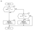
図3は、短絡判定器14がスイッチング素子1の短絡判定を行なう際に実行する処理手順の一例を示すフローチャートである。このフローチャートは、スイッチング素子1のターンオン動作中において、予め定められた条件が成立する毎(たとえば予め定められた周期毎)に繰り返し実行される。なお、短絡判定器14の処理は、ソフトウェア処理によって実現されてもよいし、専用のハードウェア(電子回路)の処理で実現されてもよい。
Figure 3 is a flowchart showing an example of a processing procedure executed by the
短絡判定器14は、第1比較装置U1の出力信号S1がハイ状態である時に第2比較装置U2の出力信号S2がロー状態からハイ状態に変化したか否かを判定する(ステップS10)。The short-
出力信号S1がハイ状態である時に出力信号S2がロー状態からハイ状態に変化した場合(ステップS10においてYES)、すなわち、コンデンサ電圧が基準値VQRよりも大きい時にゲート電圧が基準値VQRに達した場合、短絡判定器14は、スイッチング素子1が短絡状態であると判定してハイ信号を指令部2に出力する(ステップS12)。If the output signal S2 changes from a low state to a high state while the output signal S1 is in a high state (YES in step S10), i.e., if the gate voltage reaches the reference value VQR when the capacitor voltage is greater than the reference value VQR, the short-
一方、ステップS10においてNOと判定された場合、短絡判定器14は、第2比較装置U2の出力信号S2がロー状態である時に第1比較装置U1の出力信号S1がハイ状態からロー状態に変化したか否かを判定する(ステップS14)。On the other hand, if the result of the judgment in step S10 is NO, the short-
出力信号S2がロー状態である時に出力信号S1がハイ状態からロー状態に変化した場合(ステップS14においてYES)、すなわち、ゲート電圧が基準値VR以下である時にコンデンサ電圧が基準値VQRよりも大きい値から基準値VQRに低下した場合、短絡判定器14は、スイッチング素子1が通常状態でありミラー期間に突入したと判定してロー信号を指令部2にする(ステップS16)。If the output signal S1 changes from a high state to a low state while the output signal S2 is in a low state (YES in step S14), that is, if the capacitor voltage drops from a value greater than the reference value VQR to the reference value VQR while the gate voltage is equal to or less than the reference value VR, the short-
なお、指令部2は、短絡判定器14からハイ信号(スイッチング素子1が短絡状態であることを示す信号)を受けた場合、上述のオフ指令(スイッチング素子15をオン状態にし、スイッチング素子5をオフ状態にし、スイッチング素子6をオン状態にするための指令)を各スイッチング素子5,6,15に出力する。これにより、スイッチング素子1の短絡状態を解消することができる。
When the
さらに、本実施の形態による駆動装置100においては、コンデンサ4の容量Cbが、下記の関係式(2)を満たすように設計される。
Furthermore, in the
|Voff-Von|×Ci≧|Vc-Von|×Cb …(2)
上記の関係式(2)において、「Ci」はスイッチング素子1の入力容量(ゲートソース間容量とゲートドレイン間容量とを合計した全体の容量)を表わし、「Vc」はコンデンサ充電電圧(コンデンサ電圧の初期値)を表わす。なお、負バイアス電位Voff、駆動電圧Von、コンデンサ4の容量Cbは、上述したとおりである。
|Voff-Von|×Ci≧|Vc-Von|×Cb…(2)
In the above relational expression (2), "Ci" represents the input capacitance of the switching element 1 (the total capacitance obtained by adding up the gate-source capacitance and the gate-drain capacitance), and "Vc" represents the capacitor charging voltage (capacitor voltage The negative bias potential Voff, the drive voltage Von, and the capacitance Cb of the
関係式(2)の左辺は、スイッチング素子1のゲート電圧が、負バイアス電位Voffから駆動電圧Vonに上昇するために必要な電荷量に相当する。
The left side of the relational equation (2) corresponds to the amount of charge required for the gate voltage of the
関係式(2)の右辺は、コンデンサ電圧が初期値Vcから駆動電圧Vonに低下するまでにコンデンサ4が放出する電荷量に相当する。
The right side of equation (2) corresponds to the amount of charge released by
仮に上記の関係式(2)を満たさない場合、ゲート電圧が駆動電圧Vonよりも高い電圧になるため、スイッチング素子1内の酸化膜の寿命低下を招く可能性がある。If the above relationship (2) is not satisfied, the gate voltage will be higher than the drive voltage Von, which may result in a shortened lifespan of the oxide film in the
これに対し、本実施の形態においては、上記の関係式(2)を満たす。これにより、スイッチング素子1のスイッチング動作中にコンデンサ電圧が駆動電圧Vonに低下し、ダイオード8が導通する状態となる。そのため、スイッチング素子1の定常オン状態のゲート電圧を駆動電圧Von(電圧源7の出力電圧)に安定させることができる。その結果、スイッチング素子1内の酸化膜の寿命低下を抑制することができる。In contrast, in the present embodiment, the above relational expression (2) is satisfied. As a result, the capacitor voltage drops to the drive voltage Von during the switching operation of the
以上のように、本実施の形態1による駆動装置100は、電圧源3(第1電圧源)と、スイッチング素子15と、スイッチング素子15を介して電圧源3と並列に接続されるコンデンサ4と、コンデンサ4と電力用のスイッチング素子1のゲート端子との間に設けられたスイッチング素子5,6(切替装置)と、コンデンサ4の電圧と基準値VQRとの比較結果を示す信号S1を出力する第1比較装置U1と、スイッチング素子1のゲート電圧と基準値VRとの比較結果を示す信号S2を出力する第2比較装置U2と、第1比較装置U1の出力信号S1と第2比較装置U2の出力信号S2とを用いてスイッチング素子1が短絡状態であるか否かを判定する短絡判定器14とを備える。As described above, the driving
この構成によれば、コンデンサ4の電圧と基準値VQRとの比較結果(第1比較装置U1の出力信号S1)と、スイッチング素子1のゲート電圧と基準値VRとの比較結果(第2比較装置U2の出力信号S2)とを用いて、スイッチング素子1の短絡状態を判定する。そのため、積分器が不要となり回路の簡略化ができる。
According to this configuration, the short-circuit state of the
実施の形態2.
図4は、本実施の形態2による駆動装置100Aを有する半導体装置DAの一例を示す図である。図4に示す駆動装置100Aは、上述の図1に示す駆動装置100に対して、負バイアス電位Voffを出力する電圧源9を削除するとともに、スイッチング素子6をオフ抵抗20に置き換えたものである。駆動装置100Aのその他の構成は、上述の駆動装置100の構成と同じであるため、ここでの詳細な説明は繰返さない。
Fig. 4 is a diagram showing an example of a semiconductor device DA having a driving
この駆動装置100Aにおいては、スイッチング素子1をオフ状態にする場合、指令部2は、スイッチング素子5をオフ状態にする。これにより、駆動装置100Aの出力端子17,18間の電圧は、ゲート抵抗16およびオフ抵抗20によって0Vへ低下する。そのため、スイッチング素子1のゲート電圧がしきい電圧を下回り、スイッチング素子1がオフ状態となる。In this
このように、駆動装置100の構成を簡素化した駆動装置100Aを採用するようにしてもよい。In this way, it is possible to adopt a
実施の形態3.
上述の実施の形態1では、スイッチング素子1のゲート電荷量とゲート電圧との関係(図2参照)を利用してスイッチング素子1の短絡判定を行なう例について説明した。
In the above-described first embodiment, an example has been described in which a short circuit determination of the
これに対し、本実施の形態3では、スイッチング素子1のゲート電荷量とゲート電流との関係を利用してスイッチング素子1の短絡判定を行なう。In contrast, in this
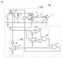
図5は、本実施の形態3による駆動装置100Bを有する半導体装置DBの一例を示す図である。図5に示す駆動装置100Bは、上述の図1に示す駆動装置100に対して、第1比較装置U1および第2比較装置U2を、それぞれ第1比較装置U1Bおよび第2比較装置U2Bに置き換えたものである。駆動装置100Bのその他の構成は、上述の駆動装置100の構成と同じであるため、ここでの詳細な説明は繰返さない。
Figure 5 is a diagram showing an example of a semiconductor device DB having a driving
第1比較装置U1Bは、比較部10aおよび電圧源11aと、比較部10bおよび電圧源11bと、論理回路60とを備える。電圧源11aは、基準値Vrq1に対応する電圧を比較部10aに出力する。比較部10aは、コンデンサ電圧と電圧源11aが出力する電圧との比較結果を論理回路60に出力する。電圧源11bは、基準値Vrq2に対応する電圧を比較部10bに出力する。比較部10bは、コンデンサ電圧と電圧源11bが出力する電圧との比較結果を論理回路60に出力する。論理回路60は、比較部10a,10bの出力の論理積を取ることで、ゲート電荷量が基準値Vrq1から基準値Vrq2までの範囲内にあることを検出することができる。論理回路60は検出結果を短絡判定器14に出力する。The first comparison device U1B includes a
第2比較装置U2Bは、微分器30と、比較部31と、電圧源32とを備える。微分器30は、コンデンサ4と比較部31との間に設けられ、コンデンサ電圧を微分した値を比較部31に出力する。なお、微分器30の出力(コンデンサ電圧の微分値)は、スイッチング素子1のゲート電流(駆動装置100Bからスイッチング素子1のゲートに流れる電流)に相当する。電圧源32は、基準値Vriに対応する電圧を比較部31に出力する。比較部31は、微分器30の出力(ゲート電流に相当する値)と電圧源32が出力する電圧と比較することで、ゲート電流が基準値Vri未満であることを検出することができる。比較部31は、比較結果を短絡判定器14に出力する。The second comparison device U2B includes a
図5に示す駆動装置100Bにおいても、積分器を使用することなくスイッチング素子1の短絡検出が可能となり、設計の自由度が向上する。In the
図6は、スイッチング素子1のターンオン動作時における、ゲート電荷量とゲート電流との関係の一例を示す図である。図6において、スイッチング素子1の通常時の関係が破線L5で表わされ、スイッチング素子1のアーム短絡時の関係が実線L6で表わされる。
Figure 6 is a diagram showing an example of the relationship between the gate charge and the gate current during the turn-on operation of the
通常時は、上述したミラー期間の存在により、破線L5に示すように、ゲート電流の変化率がごく緩やかになる期間(ゲート電流が電流値Imでほぼ一定となる期間)が発生する。一方、アーム短絡時には、ミラー期間がないため、実線L6に示すように、ゲート電流はそのまま単調に低下する。Under normal circumstances, due to the existence of the mirror period described above, there is a period during which the rate of change of the gate current is very gradual (a period during which the gate current is almost constant at the current value Im), as shown by the dashed line L5. On the other hand, when the arm is short-circuited, there is no mirror period, so the gate current continues to decrease monotonically, as shown by the solid line L6.
破線L5と実線L6との違いを判定できるように、ゲート電流の基準値Vri、ゲート電荷量の基準値Vrq1,Vrq2で囲まれた範囲が図6に示す斜線部分となるように電圧源11a,11b,32の各出力電圧を設定することによって、スイッチング素子1の短絡判定を行なうことができる。In order to be able to determine the difference between the dashed line L5 and the solid line L6, the output voltages of the
以上のように、図5に示す駆動装置100Bにおいては、コンデンサ電圧を微分することでゲート電流値を求め、このゲート電流を用いてスイッチング素子1の短絡判定を行なうことができる。そのため、駆動装置100Bにおいても、積分器を使用することなくスイッチング素子1の短絡判定を行なうことができる。As described above, in the
実施の形態4.
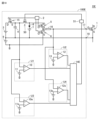
図7は、本実施の形態4による駆動装置100Cを有する半導体装置DCの一例を示す図である。図7に示す駆動装置100Cは、上述の図1に示す駆動装置100に対して、比較部10,12の入力部分にそれぞれフィルタ40,41を追加したものである。駆動装置100Cのその他の構成は、上述の駆動装置100の構成と同じであるため、ここでの詳細な説明は繰返さない。
Fig. 7 is a diagram showing an example of a semiconductor device DC having a driving
比較部10,12は、回路外部からの放射ノイズなど、ノイズによって誤動作する可能性がある。そのため、比較部10,12の入力部分にそれぞれフィルタ40,41を挿入することで、誤動作の発生しにくい構成とすることができる。The
また、図7には図1に示す駆動装置100を元に変形した例を示したが、他の駆動装置100A,100Bにおける比較部または微分器の入力部分にフィルタを挿入することで同様の効果を得ることができる。
Although Figure 7 shows an example of a modification based on the
実施の形態5.
上述の実施の形態1~4では、いずれにおいてもミラー期間の有無を判定することによって、スイッチング素子1の短絡状態を検出する。
In any of the above-described first to fourth embodiments, the short-circuit state of the
これに対し、本実施の形態5では、ミラー期間を検出した場合に、駆動装置100の出力電圧を減少させることによって、スイッチング素子1のスイッチング速度が必要以上に高くなることを防ぎ、ドレイン電圧の時間変化率を減少させる。In contrast, in this
図8は、本実施の形態5による駆動装置100Dを有する半導体装置DDの一例を示す図である。図8に示す駆動装置100Dは、上述の図1に示す駆動装置100に対して、スイッチング素子50および制御部51を追加するとともに、短絡判定器14の出力を制御部51に入力するようにしたものである。駆動装置100Dのその他の構成は、上述の駆動装置100の構成と同じであるため、ここでの詳細な説明は繰返さない。
Figure 8 is a diagram showing an example of a semiconductor device DD having a
コンデンサ4は、MOSFETであるスイッチング素子50を介して、スイッチング素子5に接続される。制御部51は、短絡判定器14からロー信号を受けた場合(すなわちミラー期間への突入が検出された場合)に、スイッチング素子50をオフ状態にしてコンデンサ4からスイッチング素子5への電荷の供給を切断する。これにより、ミラー期間への突入が検出された場合に、駆動装置100Dの出力電圧は電圧源7から出力される駆動電圧Vonに切り替えられる。そのため、その後のスイッチング素子1のスイッチング速度を抑えることができ、ノイズの原因となる主電圧の変化速度(単位時間あたりの変化量)を抑制することができる。The
図9は、スイッチング素子1のターンオン動作時における、スイッチング素子1のゲート電荷量とゲート電圧との関係の一例を示す図である。図9においては、基準値VRよりも高いミラー電圧となる電流値をスイッチングした場合の関係が実線L7で示され、基準値VRよりも低いミラー電圧となる電流値をスイッチングした場合の関係が破線L8で示される。
Figure 9 is a diagram showing an example of the relationship between the gate charge and gate voltage of switching
基準値VRよりも高いミラー電圧となる電流値をスイッチングした場合、実線L7に示すように、ゲート電圧が基準値VRよりも低くかつゲート電荷量が基準値QRよりも高くなる領域は存在しないため、スイッチング速度は低下せず、ターンオン損失を増加させることはない。When switching a current value that results in a mirror voltage higher than the reference value VR, as shown by the solid line L7, there is no region where the gate voltage is lower than the reference value VR and the gate charge amount is higher than the reference value QR, so the switching speed does not decrease and the turn-on loss does not increase.
一方、基準値VRよりも低いミラー電圧となる電流値をスイッチングした場合、破線L8に示すように、ゲート電圧が基準値VRよりも低くかつゲート電荷量が基準値QRよりも高くなる領域が存在する。この領域が検出された場合、短絡判定器14は、ミラー期間に突入したと判定し、ロー信号を制御部51に出力する。制御部51は、短絡判定器14からロー信号を受けると、スイッチング素子50をターンオフする。これにより、駆動装置100Dの出力電圧は、コンデンサ4の両端電圧から電圧源7の駆動電圧Vonへ低下するため、スイッチング素子1の主電圧の変化速度(単位時間あたりの変化量)を抑制することができる。On the other hand, when a current value that results in a mirror voltage lower than the reference value VR is switched, as shown by the dashed line L8, there is a region in which the gate voltage is lower than the reference value VR and the gate charge amount is higher than the reference value QR. When this region is detected, the short-
実施の形態6.
図10は、本実施の形態6による駆動装置100Eを有する半導体装置DEの一例を示す図である。図10に示す駆動装置100Eは、上述の図8に示す駆動装置100Dに対して、第3比較装置U3および第4比較装置U4を追加し、短絡判定器14を短絡判定器14Eに変更したものである。駆動装置100Eのその他の構成は、上述の駆動装置100Dの構成と同じであるため、ここでの詳細な説明は繰返さない。
Fig. 10 is a diagram showing an example of a semiconductor device DE having a
上述の実施の形態5では、基準値VRよりも低いミラー電流となるスイッチングでは、ミラー期間が終了してから短絡判定器14がハイ信号を出力してしまい、スイッチング素子1の主電圧の変化率の抑制が不十分となる条件が発生する可能性がある。In the above-mentioned
図11は、スイッチング素子1のターンオン動作時における、スイッチング素子1のゲート電荷量とゲート電圧との関係の一例を示す図である。図11においては、基準値VRよりも低くかつ基準値VR2よりも高いミラー電圧となる電流値をスイッチングした場合の関係が実線L9で示され、基準値VR,VR2よりも低いミラー電圧となる電流値をスイッチングした場合の関係が破線L10で示される。
Figure 11 is a diagram showing an example of the relationship between the gate charge and gate voltage of switching
図11に示す例において、ゲート電荷量の基準値QRおよびゲート電圧の基準値VRでミラー期間を判定する場合、電流の小さい破線L10の波形において、ゲート電圧が基準値VRよりも低くかつゲート電荷量が基準値QRよりも高くなるタイミング(すなわちミラー期間の検出タイミング)が、ミラー期間が終了した後になってしまう。In the example shown in Figure 11, when the mirror period is determined using the reference value QR of the gate charge and the reference value VR of the gate voltage, in the waveform of the dashed line L10, which has a small current, the timing at which the gate voltage becomes lower than the reference value VR and the gate charge becomes higher than the reference value QR (i.e., the detection timing of the mirror period) occurs after the mirror period has ended.
そこで、本実施の形態6においては、第1比較装置U1および第2比較装置U2に加えて、第3比較装置U3および第4比較装置U4を備える。Therefore, in this
第3比較装置U3は、比較部10eと電圧源11eとを備える。電圧源11eは、基準値VQRとは異なる基準値(ゲート電荷量が基準値QRよりも低い値QR2となる時のゲート電圧の値)を比較部10eに出力する。比較部10eは、コンデンサ電圧を電圧源11が出力する電圧との比較結果を示す信号S3を短絡判定器14Eに出力する。The third comparison device U3 includes a comparison unit 10e and a
第4比較装置U4は、比較部12eと電圧源13eとを備える。電圧源13eは、基準値VRよりも低い基準値VR2の電圧を比較部12eに出力する。比較部12eは、スイッチング素子1のゲート電圧と、電圧源13eが出力する電圧との比較結果を示す信号S4を短絡判定器14Eに出力する。The fourth comparison device U4 includes a
短絡判定器14Eは、第1比較装置U1の出力信号S1、第2比較装置U2の出力信号S2、第3比較装置U3の出力信号S3、および第4比較装置U4の出力信号S4を用いて、スイッチング素子1のミラー期間を検出する。The
制御部51は、短絡判定器14Eがスイッチング素子1のミラー期間を検出した場合に、スイッチング素子50をターンオフする。
The
このように、実施の形態6においては、第3比較装置U3および第4比較装置U4を追加で備えることで、電流の大きさの異なる条件においても適切にミラー期間を検出して駆動装置100Dの出力電圧を低下させることができる。そのため、電流の大きさの異なる条件においてもスイッチング素子1の主電圧の変化速度(単位時間あたりの変化量)を適切に抑制することができる。In this way, in the sixth embodiment, by additionally providing the third comparison device U3 and the fourth comparison device U4, it is possible to appropriately detect the mirror period and reduce the output voltage of the
実施の形態7.
本実施の形態7は、上述した実施の形態1~6による半導体装置D~DEのいずれかを電力変換装置に適用したものである。以下、実施の形態7として、三相のインバータに本開示を適用した場合について説明する。
In the seventh embodiment, any one of the semiconductor devices D to DE according to the first to sixth embodiments is applied to a power conversion device. Hereinafter, as the seventh embodiment, a case in which the present disclosure is applied to a three-phase inverter will be described.
図12は、本実施の形態7による電力変換装置を適用した電力変換システムの構成を示すブロック図である。
Figure 12 is a block diagram showing the configuration of a power conversion system to which a power conversion device according to this
図12に示す電力変換システムは、電源1000と、電力変換装置2000と、負荷3000とを備える。電源1000は、直流電源であり、電力変換装置2000に直流電力を供給する。電源1000は種々のもので構成することが可能であり、例えば、直流系統、太陽電池、蓄電池で構成することができるし、交流系統に接続された整流回路やAC/DCコンバータで構成することとしてもよい。また、電源1000を、直流系統から出力される直流電力を負荷3000が使用可能な電力に変換するDC/DCコンバータによって構成することとしてもよい。The power conversion system shown in FIG. 12 includes a
電力変換装置2000は、電源1000と負荷3000との間に接続された三相のインバータであり、電源1000から供給された直流電力を交流電力に変換し、負荷3000に交流電力を供給する。電力変換装置2000は、図12に示すように、直流電力を交流電力に変換して出力する主変換回路2010と、主変換回路2010を制御する制御信号を主変換回路2010に出力する制御回路2030とを備えている。The
負荷3000は、電力変換装置2000から供給された交流電力によって駆動される三相の電動機である。なお、負荷3000は、各種電気機器に搭載された電動機であり、例えば、ハイブリッド自動車や電気自動車、鉄道車両、エレベーター、もしくは、空調機器向けの電動機として用いられる。The
以下、電力変換装置2000の詳細を説明する。主変換回路2010は、スイッチング素子を備えており(図示せず)、スイッチング素子がスイッチングすることによって、電源1000から供給される直流電力を交流電力に変換し、負荷3000に供給する。主変換回路2010の具体的な回路構成は種々のものがあるが、本実施の形態にかかる主変換回路2010は2レベルの三相フルブリッジ回路であり、6つのスイッチング素子とそれぞれのスイッチング素子に逆並列された6つの還流ダイオードから構成することができる。主変換回路2010は、各スイッチング素子および各スイッチング素子を駆動する駆動装置を有する半導体装置2020を備える。半導体装置2020に備えられる各スイッチング素子および各駆動装置は、上述した実施の形態1~6による半導体装置D~DEのいずれかが有するスイッチング素子1および駆動装置である。6つのスイッチング素子は2つのスイッチング素子ごとに直列接続され上下アームを構成し、各上下アームはフルブリッジ回路の各相(U相、V相、W相)を構成する。そして、各上下アームの出力端子、すなわち主変換回路2010の3つの出力端子は、負荷3000に接続される。The
制御回路2030は、負荷3000に所望の電力が供給されるよう主変換回路2010のスイッチング素子を制御する。具体的には、負荷3000に供給すべき電力に基づいて主変換回路2010の各スイッチング素子がオン状態となるべき時間(オン時間)を算出する。例えば、出力すべき電圧に応じてスイッチング素子のオン時間を変調するPWM制御によって主変換回路2010を制御することができる。そして、各時点においてオン状態となるべきスイッチング素子にはオン信号を、オフ状態となるべきスイッチング素子にはオフ信号が出力されるよう、主変換回路2010が備える駆動回路に制御指令(制御信号)を出力する。駆動回路は、この制御信号に従い、各スイッチング素子の制御電極にオン信号又はオフ信号を駆動信号として出力する。The
本実施の形態7による電力変換装置では、主変換回路2010を構成する半導体装置2020として実施の形態1~6のいずれかにかかる半導体装置を適用するため、実施の形態1~6と同様、電力用のスイッチング素子の短絡状態を、積分器を使用することなく簡素な回路で検出することができる。In the power conversion device according to the seventh embodiment, a semiconductor device according to any one of the first to sixth embodiments is applied as the
本実施の形態7では、2レベルの三相インバータに本開示を適用する例を説明したが、本開示は、これに限られるものではなく、種々の電力変換装置に適用することができる。本実施の形態7では、2レベルの電力変換装置としたが3レベルやマルチレベルの電力変換装置であっても構わないし、単相負荷に電力を供給する場合には単相のインバータに本開示を適用しても構わない。また、直流負荷等に電力を供給する場合にはDC/DCコンバータやAC/DCコンバータに本開示を適用することも可能である。In the seventh embodiment, an example of applying the present disclosure to a two-level three-phase inverter has been described, but the present disclosure is not limited to this and can be applied to various power conversion devices. In the seventh embodiment, a two-level power conversion device is described, but a three-level or multi-level power conversion device may also be used, and the present disclosure may be applied to a single-phase inverter when supplying power to a single-phase load. In addition, the present disclosure can also be applied to a DC/DC converter or an AC/DC converter when supplying power to a DC load or the like.
また、本開示を適用した電力変換装置は、上述した負荷が電動機の場合に限定されるものではなく、例えば、放電加工機やレーザー加工機、又は誘導加熱調理器や非接触給電システムの電源装置として用いることもでき、さらには太陽光発電システムや蓄電システム等のパワーコンディショナーとして用いることも可能である。 Furthermore, the power conversion device to which the present disclosure is applied is not limited to the case where the above-mentioned load is an electric motor, but can also be used, for example, as a power supply device for an electric discharge machine, a laser processing machine, an induction heating cooker, or a non-contact power supply system, and can even be used as a power conditioner for a solar power generation system, a power storage system, etc.
今回開示された実施の形態はすべての点で例示であって制限的なものではないと考えられるべきである。本開示の範囲は上記した説明ではなくて請求の範囲によって示され、請求の範囲と均等の意味および範囲内でのすべての変更が含まれることが意図される。The embodiments disclosed herein should be considered to be illustrative and not restrictive in all respects. The scope of the present disclosure is indicated by the claims, not the above description, and is intended to include all modifications within the meaning and scope of the claims.
1,5,6,15,50 スイッチング素子、2 指令部、3,7,9,11,11a,11b,11e,13,13e,32 電圧源、4 コンデンサ、8 ダイオード、10,10a,10b,10e,12,12e,31 比較部、14,14E 短絡判定器、16 ゲート抵抗、17,18 出力端子、20 オフ抵抗、30 微分器、40,41 フィルタ、51 制御部、60 論理回路、100,100A,100B,100C,100D,100E 駆動装置、1000 電源、2000 電力変換装置、2010 主変換回路、2020,D,DA,DB,DC,DD,DE 半導体装置、2030 制御回路、3000 負荷、U1,U1B 第1比較装置、U2,U2B 第2比較装置、U3 第3比較装置、U4 第4比較装置。1, 5, 6, 15, 50 Switching element, 2 Command unit, 3, 7, 9, 11, 11a, 11b, 11e, 13, 13e, 32 Voltage source, 4 Capacitor, 8 Diode, 10, 10a, 10b, 10e, 12, 12e, 31 Comparison unit, 14, 14E Short circuit determination unit, 16 Gate resistor, 17, 18 Output terminal, 20 OFF resistor, 30 Differentiator, 40, 41 Filter, 51 Control unit, 60 Logic circuit, 100, 100A, 100B, 100C, 100D, 100E Drive unit, 1000 Power supply, 2000 Power conversion unit, 2010 Main conversion circuit, 2020, D, DA, DB, DC, DD, DE Semiconductor device, 2030 Control circuit, 3000 Load, U1, U1B first comparison device, U2, U2B second comparison device, U3 third comparison device, U4 fourth comparison device.
Claims (10)
第1電圧源と、
スイッチング素子と、
前記スイッチング素子を介して前記第1電圧源と並列に接続されるコンデンサと、
前記コンデンサと前記半導体素子の前記ゲート端子との間に設けられ、前記ゲート端子に印加される電圧を切替可能に構成される切替装置と、
前記コンデンサの電圧と第1基準値との比較結果を示す信号を出力する第1比較装置と、
前記ゲート端子の電圧または前記コンデンサの電圧を微分した値と第2基準値との比較結果を示す信号を出力する第2比較装置と、
前記第1比較装置の出力信号と前記第2比較装置の出力信号とを用いて前記半導体素子が短絡状態であるか否かを判定する判定器と、
を備える、半導体素子の駆動装置。 A drive device for a power semiconductor element having a gate terminal, comprising:
A first voltage source;
A switching element;
a capacitor connected in parallel with the first voltage source via the switching element;
a switching device provided between the capacitor and the gate terminal of the semiconductor element, the switching device being configured to be able to switch a voltage applied to the gate terminal;
a first comparator that outputs a signal indicating a result of comparing the voltage of the capacitor with a first reference value;
a second comparator that outputs a signal indicating a result of comparing the voltage of the gate terminal or the voltage of the capacitor with a second reference value;
a determiner that determines whether or not the semiconductor element is in a short-circuit state using an output signal of the first comparison device and an output signal of the second comparison device;
A semiconductor element driving device comprising:
前記コンデンサの電圧が前記第1基準値以下である場合にロー状態を示す信号を出力し、
前記コンデンサの電圧が前記第1基準値よりも大きい場合にハイ状態を示す信号を出力し、
前記第2比較装置は、
前記ゲート端子の電圧または前記コンデンサの電圧を微分した値が前記第2基準値以下である場合にロー状態を示す信号を出力し、
前記ゲート端子の電圧または前記コンデンサの電圧を微分した値が前記第2基準値よりも大きい場合にハイ状態を示す信号を出力し、
前記判定器は、
前記第1比較装置の出力信号が前記ハイ状態である時に前記第2比較装置の出力信号が前記ロー状態から前記ハイ状態に変化した場合、前記半導体素子が短絡状態であると判定し、
前記第2比較装置の出力信号が前記ロー状態である時に前記第1比較装置の出力信号が前記ハイ状態から前記ロー状態に変化した場合、前記半導体素子が短絡状態ではないと判定する、請求項1に記載の半導体素子の駆動装置。 The first comparison device
outputting a signal indicating a low state when the voltage of the capacitor is equal to or lower than the first reference value;
outputting a signal indicating a high state when the voltage of the capacitor is greater than the first reference value;
The second comparison device
outputting a signal indicating a low state when a value obtained by differentiating the voltage of the gate terminal or the voltage of the capacitor is equal to or less than the second reference value;
outputting a signal indicating a high state when a value obtained by differentiating the voltage of the gate terminal or the voltage of the capacitor is greater than the second reference value;
The determiner is
determining that the semiconductor device is in a short-circuit state when the output signal of the second comparator changes from the low state to the high state while the output signal of the first comparator is in the high state;
2. The semiconductor element driving device according to claim 1, further comprising: a driving circuit for driving a semiconductor element, the driving circuit for driving a semiconductor element being determined to be not in a short-circuit state when the output signal of the first comparing device changes from the high state to the low state while the output signal of the second comparing device is in the low state.
前記切替装置は、前記第1電圧源および前記第2電圧源と並列に接続され、前記ゲート端子に印加される電圧を、前記第1電圧源または前記コンデンサからの正電圧と、前記第2電圧源からの負電圧との間で切替可能に構成される、請求項1または2に記載の半導体素子の駆動装置。 a second voltage source connected in series with the first voltage source;
3. The semiconductor element driving device of claim 1, wherein the switching device is connected in parallel with the first voltage source and the second voltage source and is configured to be able to switch the voltage applied to the gate terminal between a positive voltage from the first voltage source or the capacitor and a negative voltage from the second voltage source.
前記コンデンサと前記出力端子との間に設けられ、前記判定器の出力に応じて前記コンデンサと前記出力端子を切り離すように動作する切り離し装置と、
前記切り離し装置およびダイオードを介して前記コンデンサと並列に接続されるとともに前記ダイオードを介して前記出力端子に接続され、前記コンデンサの電圧よりも低い電圧を出力する安定化用の電圧源と、
をさらに備える、請求項1~3のいずれか1項に記載の半導体素子の駆動装置。 an output terminal connectable to the semiconductor element;
a disconnection device provided between the capacitor and the output terminal, the disconnection device operating to disconnect the capacitor from the output terminal in response to an output of the determiner;
a stabilizing voltage source connected in parallel to the capacitor via the disconnecting device and a diode and connected to the output terminal via the diode, the stabilizing voltage source outputting a voltage lower than a voltage of the capacitor;
The semiconductor element driving device according to any one of claims 1 to 3, further comprising:
前記ゲート端子の電圧または前記コンデンサの電圧を微分した値と、前記第2基準値とは異なる基準値との比較結果を示す信号を出力する第4比較装置とをさらに備え、
前記判定器は、前記第1比較装置の出力信号、前記第2比較装置の出力信号、前記第3比較装置の出力信号、および前記第4比較装置の出力信号を用いて前記半導体素子のミラー期間を検出し、
前記切り離し装置は、前記判定器によって前記ミラー期間が検出されたことに応じて前記コンデンサと前記出力端子とを切り離すように動作する、請求項4に記載の半導体素子の駆動装置。 a third comparator that outputs a signal indicating a result of comparing the voltage of the capacitor with a reference value different from the first reference value;
a fourth comparator that outputs a signal indicating a result of comparing a value obtained by differentiating the voltage of the gate terminal or the voltage of the capacitor with a reference value different from the second reference value;
the determiner detects a mirror period of the semiconductor element using the output signal of the first comparing device, the output signal of the second comparing device, the output signal of the third comparing device, and the output signal of the fourth comparing device;
5. The semiconductor element drive device according to claim 4, wherein the disconnection device operates to disconnect the capacitor from the output terminal in response to the Miller period being detected by the determiner.
前記コンデンサの電圧の微分値を出力する微分器と、
前記微分器の出力と前記第2基準値とを比較する比較器と、
を備える、請求項1~5のいずれか1項に記載の半導体素子の駆動装置。 The second comparison device
a differentiator that outputs a differential value of the voltage of the capacitor;
a comparator for comparing the output of the differentiator with the second reference value;
The semiconductor element driving device according to any one of claims 1 to 5, comprising:
前記コンデンサの容量Cbが、
Cb≦{|Voff-Von|/|Vc-Von|×Ci}
の関係式を満たす、請求項1~6のいずれか1項に記載の半導体素子の駆動装置。 When the voltage of the gate terminal when the semiconductor element is in an on-state is denoted as Von, the voltage of the gate terminal when the semiconductor element is in an off-state is denoted as Voff, the input capacitance of the semiconductor element is denoted as Ci, the charging voltage of the capacitor is denoted as Vc, and the capacitance of the capacitor is denoted as Cb,
The capacitance Cb of the capacitor is
Cb≦{|Voff-Von|/|Vc-Von|×Ci}
7. The semiconductor element driving device according to claim 1, which satisfies the following relational expression.
前記主変換回路を制御する制御信号を前記主変換回路に出力する制御回路と、
を備えた電力変換装置。 A main conversion circuit having the driving device and a semiconductor element according to any one of claims 1 to 8, which converts input power and outputs the converted power;
a control circuit that outputs a control signal for controlling the main conversion circuit to the main conversion circuit;
A power conversion device comprising:
Applications Claiming Priority (1)
| Application Number | Priority Date | Filing Date | Title |
|---|---|---|---|
| PCT/JP2020/033793 WO2022049772A1 (en) | 2020-09-07 | 2020-09-07 | Semiconductor element driving device, semiconductor device, and power conversion device |
Publications (2)
| Publication Number | Publication Date |
|---|---|
| JPWO2022049772A1 JPWO2022049772A1 (en) | 2022-03-10 |
| JP7523552B2 true JP7523552B2 (en) | 2024-07-26 |
Family
ID=80490893
Family Applications (1)
| Application Number | Title | Priority Date | Filing Date |
|---|---|---|---|
| JP2022546858A Active JP7523552B2 (en) | 2020-09-07 | 2020-09-07 | Semiconductor element driving device, semiconductor device, and power conversion device |
Country Status (5)
| Country | Link |
|---|---|
| US (1) | US12206401B2 (en) |
| JP (1) | JP7523552B2 (en) |
| CN (1) | CN116491039B (en) |
| DE (1) | DE112020007591T5 (en) |
| WO (1) | WO2022049772A1 (en) |
Families Citing this family (3)
| Publication number | Priority date | Publication date | Assignee | Title |
|---|---|---|---|---|
| CN117378144A (en) * | 2021-05-25 | 2024-01-09 | 三菱电机株式会社 | Semiconductor element driving method and driving device, and power conversion device |
| US12609227B2 (en) * | 2022-12-20 | 2026-04-21 | Metamagnetics, Inc. | Temperature stable magnetostatic wave RF devices and related techniques |
| KR102860088B1 (en) * | 2023-08-17 | 2025-09-15 | 한화솔루션 주식회사 | Power conversion apparatus and control method thereof |
Citations (3)
| Publication number | Priority date | Publication date | Assignee | Title |
|---|---|---|---|---|
| JP2015053749A (en) | 2013-09-05 | 2015-03-19 | 三菱電機株式会社 | Driving circuit for power semiconductor element |
| JP2018098938A (en) | 2016-12-14 | 2018-06-21 | 三菱電機株式会社 | Drive system and power conversion device |
| WO2019021590A1 (en) | 2017-07-28 | 2019-01-31 | 三菱電機株式会社 | Drive circuit for power semiconductor element |
Family Cites Families (11)
| Publication number | Priority date | Publication date | Assignee | Title |
|---|---|---|---|---|
| EP0354435B1 (en) * | 1988-08-12 | 1995-12-20 | Hitachi, Ltd. | A drive circuit for an insulated gate transistor; and its use in a switching circuit, a current switching apparatus and an induction motor system |
| JP4223331B2 (en) * | 2003-06-13 | 2009-02-12 | 株式会社日立製作所 | Protection device for power control semiconductor element and power conversion device including the same |
| JP4804142B2 (en) | 2005-12-21 | 2011-11-02 | 東洋電機製造株式会社 | High-speed gate drive circuit |
| JP2009225506A (en) * | 2008-03-13 | 2009-10-01 | Toshiba Corp | Power converter |
| CN102160271B (en) * | 2008-09-22 | 2013-11-20 | 富士通株式会社 | Control method for power control circuit, power supply unit, power supply system, and power controller control method |
| JP6300964B1 (en) * | 2017-01-13 | 2018-03-28 | 三菱電機株式会社 | Power converter |
| JP6264491B1 (en) * | 2017-05-11 | 2018-01-24 | 富士電機株式会社 | Short-circuit detection device and device |
| US11050418B2 (en) * | 2019-01-11 | 2021-06-29 | Infineon Technologies Ag | Gate level triggered desaturation blanking |
| US11519954B2 (en) * | 2019-08-27 | 2022-12-06 | Analog Devices International Unlimited Company | Apparatus and method to achieve fast-fault detection on power semiconductor devices |
| JP7530385B2 (en) * | 2019-12-12 | 2024-08-07 | ローム株式会社 | Gate drive circuit for switching circuit and control circuit for switching power supply |
| WO2022265597A1 (en) * | 2021-06-14 | 2022-12-22 | Istanbul Teknik Universitesi | A short circuit protection system for battery packs |
-
2020
- 2020-09-07 WO PCT/JP2020/033793 patent/WO2022049772A1/en not_active Ceased
- 2020-09-07 DE DE112020007591.5T patent/DE112020007591T5/en active Pending
- 2020-09-07 JP JP2022546858A patent/JP7523552B2/en active Active
- 2020-09-07 CN CN202080103745.4A patent/CN116491039B/en active Active
- 2020-09-07 US US18/015,720 patent/US12206401B2/en active Active
Patent Citations (3)
| Publication number | Priority date | Publication date | Assignee | Title |
|---|---|---|---|---|
| JP2015053749A (en) | 2013-09-05 | 2015-03-19 | 三菱電機株式会社 | Driving circuit for power semiconductor element |
| JP2018098938A (en) | 2016-12-14 | 2018-06-21 | 三菱電機株式会社 | Drive system and power conversion device |
| WO2019021590A1 (en) | 2017-07-28 | 2019-01-31 | 三菱電機株式会社 | Drive circuit for power semiconductor element |
Also Published As
| Publication number | Publication date |
|---|---|
| CN116491039B (en) | 2025-06-27 |
| CN116491039A (en) | 2023-07-25 |
| JPWO2022049772A1 (en) | 2022-03-10 |
| US12206401B2 (en) | 2025-01-21 |
| DE112020007591T5 (en) | 2023-06-22 |
| WO2022049772A1 (en) | 2022-03-10 |
| US20230261654A1 (en) | 2023-08-17 |
Similar Documents
| Publication | Publication Date | Title |
|---|---|---|
| US10038438B2 (en) | Power semiconductor element driving circuit | |
| US7777437B2 (en) | Switching control system and motor driving system | |
| JP7523552B2 (en) | Semiconductor element driving device, semiconductor device, and power conversion device | |
| JP2018182818A (en) | Switching element drive device | |
| JP6988670B2 (en) | Drive circuit, power module and power conversion system | |
| CN105896940B (en) | Power inverter | |
| US11728802B2 (en) | Drive circuit | |
| JP7471426B2 (en) | DRIVE CONTROL CIRCUIT FOR POWER SEMICONDUCTOR DEVICE, POWER SEMICONDUCTOR MODULE, AND POWER CONVERSION DEVICE | |
| CN111971884A (en) | Gate driving circuit and gate driving method | |
| JPH0923664A (en) | Inverter device | |
| CN110911229A (en) | Inductive coil drive circuit with protection function | |
| US11404953B2 (en) | Drive circuit for power semiconductor element and power semiconductor module employing the same | |
| CN115694447B (en) | Short-circuit protection for bidirectional switches | |
| CN112039505A (en) | Method for operating an electrical circuit, electrical circuit and motor vehicle | |
| CN115298943A (en) | Semiconductor drive device, semiconductor device, and power conversion device | |
| CN113056864B (en) | power conversion device | |
| JP4151163B2 (en) | MOS transistor drive circuit | |
| US20250364986A1 (en) | Programmable gate voltage for on resistance control of power module | |
| US20240258901A1 (en) | Gate drive circuit and power conversion device | |
| US20250226815A1 (en) | Drive circuit and control method for drive circuit | |
| US20250364984A1 (en) | Programmable gate voltage for on resistance control of power module | |
| US20250274056A1 (en) | Method of operating an inverter circuit, inverter arrangement and drive unit | |
| WO2023157185A1 (en) | Gate drive circuit and power conversion device | |
| CN118353337A (en) | Gate drive with phase slew rate control and over-current protection | |
| CN116470895A (en) | Components of solid state contactors and three-phase solid state contactors |
Legal Events
| Date | Code | Title | Description |
|---|---|---|---|
| A621 | Written request for application examination |
Free format text: JAPANESE INTERMEDIATE CODE: A621 Effective date: 20230202 |
|
| A131 | Notification of reasons for refusal |
Free format text: JAPANESE INTERMEDIATE CODE: A131 Effective date: 20240227 |
|
| A521 | Request for written amendment filed |
Free format text: JAPANESE INTERMEDIATE CODE: A523 Effective date: 20240410 |
|
| TRDD | Decision of grant or rejection written | ||
| A01 | Written decision to grant a patent or to grant a registration (utility model) |
Free format text: JAPANESE INTERMEDIATE CODE: A01 Effective date: 20240618 |
|
| A61 | First payment of annual fees (during grant procedure) |
Free format text: JAPANESE INTERMEDIATE CODE: A61 Effective date: 20240716 |
|
| R150 | Certificate of patent or registration of utility model |
Ref document number: 7523552 Country of ref document: JP Free format text: JAPANESE INTERMEDIATE CODE: R150 |