JP7463173B2 - 画像形成装置 - Google Patents
画像形成装置 Download PDFInfo
- Publication number
- JP7463173B2 JP7463173B2 JP2020067875A JP2020067875A JP7463173B2 JP 7463173 B2 JP7463173 B2 JP 7463173B2 JP 2020067875 A JP2020067875 A JP 2020067875A JP 2020067875 A JP2020067875 A JP 2020067875A JP 7463173 B2 JP7463173 B2 JP 7463173B2
- Authority
- JP
- Japan
- Prior art keywords
- recording material
- image
- secondary transfer
- voltage
- image forming
- Prior art date
- Legal status (The legal status is an assumption and is not a legal conclusion. Google has not performed a legal analysis and makes no representation as to the accuracy of the status listed.)
- Active
Links
- 238000012546 transfer Methods 0.000 claims description 236
- 239000000463 material Substances 0.000 claims description 165
- 238000001514 detection method Methods 0.000 claims description 34
- 238000012360 testing method Methods 0.000 claims description 21
- 239000003086 colorant Substances 0.000 claims description 4
- 230000003287 optical effect Effects 0.000 claims 2
- 238000009751 slip forming Methods 0.000 claims 1
- 238000000034 method Methods 0.000 description 38
- 230000008569 process Effects 0.000 description 35
- 230000032258 transport Effects 0.000 description 30
- 239000000123 paper Substances 0.000 description 18
- 238000004364 calculation method Methods 0.000 description 17
- 230000003595 spectral effect Effects 0.000 description 16
- 230000015572 biosynthetic process Effects 0.000 description 15
- 230000008859 change Effects 0.000 description 12
- 238000010586 diagram Methods 0.000 description 10
- 238000012545 processing Methods 0.000 description 10
- 230000004044 response Effects 0.000 description 7
- 229920001971 elastomer Polymers 0.000 description 6
- 239000010410 layer Substances 0.000 description 6
- 238000011144 upstream manufacturing Methods 0.000 description 6
- 238000012937 correction Methods 0.000 description 5
- 230000006870 function Effects 0.000 description 5
- 239000005060 rubber Substances 0.000 description 5
- 239000002344 surface layer Substances 0.000 description 5
- 230000000007 visual effect Effects 0.000 description 4
- 229910052745 lead Inorganic materials 0.000 description 3
- 239000002245 particle Substances 0.000 description 3
- 229920005989 resin Polymers 0.000 description 3
- 239000011347 resin Substances 0.000 description 3
- 230000002159 abnormal effect Effects 0.000 description 2
- 238000010521 absorption reaction Methods 0.000 description 2
- 238000004737 colorimetric analysis Methods 0.000 description 2
- 230000000694 effects Effects 0.000 description 2
- 230000005684 electric field Effects 0.000 description 2
- 230000007613 environmental effect Effects 0.000 description 2
- 239000007787 solid Substances 0.000 description 2
- 239000004642 Polyimide Substances 0.000 description 1
- 229920006311 Urethane elastomer Polymers 0.000 description 1
- 239000002216 antistatic agent Substances 0.000 description 1
- 229920005549 butyl rubber Polymers 0.000 description 1
- 239000006229 carbon black Substances 0.000 description 1
- 238000006243 chemical reaction Methods 0.000 description 1
- 239000006258 conductive agent Substances 0.000 description 1
- 230000001186 cumulative effect Effects 0.000 description 1
- 230000007547 defect Effects 0.000 description 1
- 239000013013 elastic material Substances 0.000 description 1
- 239000000806 elastomer Substances 0.000 description 1
- 238000005516 engineering process Methods 0.000 description 1
- 239000003822 epoxy resin Substances 0.000 description 1
- 239000004744 fabric Substances 0.000 description 1
- -1 fluororesin Substances 0.000 description 1
- 229920001821 foam rubber Polymers 0.000 description 1
- 238000005286 illumination Methods 0.000 description 1
- 238000003384 imaging method Methods 0.000 description 1
- 239000004973 liquid crystal related substance Substances 0.000 description 1
- 230000007774 longterm Effects 0.000 description 1
- 230000014759 maintenance of location Effects 0.000 description 1
- 238000005259 measurement Methods 0.000 description 1
- 239000002184 metal Substances 0.000 description 1
- 229910052751 metal Inorganic materials 0.000 description 1
- 239000002985 plastic film Substances 0.000 description 1
- 229920006255 plastic film Polymers 0.000 description 1
- 229920000515 polycarbonate Polymers 0.000 description 1
- 239000004417 polycarbonate Substances 0.000 description 1
- 229920000647 polyepoxide Polymers 0.000 description 1
- 229920000728 polyester Polymers 0.000 description 1
- 229920001721 polyimide Polymers 0.000 description 1
- 229920002635 polyurethane Polymers 0.000 description 1
- 239000004814 polyurethane Substances 0.000 description 1
- 239000000843 powder Substances 0.000 description 1
- 238000003825 pressing Methods 0.000 description 1
- 229920002379 silicone rubber Polymers 0.000 description 1
- 239000004945 silicone rubber Substances 0.000 description 1
- 230000003068 static effect Effects 0.000 description 1
- 230000001360 synchronised effect Effects 0.000 description 1
Images


Classifications
-
- G—PHYSICS
- G03—PHOTOGRAPHY; CINEMATOGRAPHY; ANALOGOUS TECHNIQUES USING WAVES OTHER THAN OPTICAL WAVES; ELECTROGRAPHY; HOLOGRAPHY
- G03G—ELECTROGRAPHY; ELECTROPHOTOGRAPHY; MAGNETOGRAPHY
- G03G15/00—Apparatus for electrographic processes using a charge pattern
- G03G15/14—Apparatus for electrographic processes using a charge pattern for transferring a pattern to a second base
- G03G15/16—Apparatus for electrographic processes using a charge pattern for transferring a pattern to a second base of a toner pattern, e.g. a powder pattern, e.g. magnetic transfer
- G03G15/1605—Apparatus for electrographic processes using a charge pattern for transferring a pattern to a second base of a toner pattern, e.g. a powder pattern, e.g. magnetic transfer using at least one intermediate support
-
- G—PHYSICS
- G03—PHOTOGRAPHY; CINEMATOGRAPHY; ANALOGOUS TECHNIQUES USING WAVES OTHER THAN OPTICAL WAVES; ELECTROGRAPHY; HOLOGRAPHY
- G03G—ELECTROGRAPHY; ELECTROPHOTOGRAPHY; MAGNETOGRAPHY
- G03G15/00—Apparatus for electrographic processes using a charge pattern
- G03G15/50—Machine control of apparatus for electrographic processes using a charge pattern, e.g. regulating differents parts of the machine, multimode copiers, microprocessor control
- G03G15/5054—Machine control of apparatus for electrographic processes using a charge pattern, e.g. regulating differents parts of the machine, multimode copiers, microprocessor control by measuring the characteristics of an intermediate image carrying member or the characteristics of an image on an intermediate image carrying member, e.g. intermediate transfer belt or drum, conveyor belt
- G03G15/5058—Machine control of apparatus for electrographic processes using a charge pattern, e.g. regulating differents parts of the machine, multimode copiers, microprocessor control by measuring the characteristics of an intermediate image carrying member or the characteristics of an image on an intermediate image carrying member, e.g. intermediate transfer belt or drum, conveyor belt using a test patch
-
- G—PHYSICS
- G03—PHOTOGRAPHY; CINEMATOGRAPHY; ANALOGOUS TECHNIQUES USING WAVES OTHER THAN OPTICAL WAVES; ELECTROGRAPHY; HOLOGRAPHY
- G03G—ELECTROGRAPHY; ELECTROPHOTOGRAPHY; MAGNETOGRAPHY
- G03G15/00—Apparatus for electrographic processes using a charge pattern
- G03G15/14—Apparatus for electrographic processes using a charge pattern for transferring a pattern to a second base
- G03G15/16—Apparatus for electrographic processes using a charge pattern for transferring a pattern to a second base of a toner pattern, e.g. a powder pattern, e.g. magnetic transfer
- G03G15/1665—Apparatus for electrographic processes using a charge pattern for transferring a pattern to a second base of a toner pattern, e.g. a powder pattern, e.g. magnetic transfer by introducing the second base in the nip formed by the recording member and at least one transfer member, e.g. in combination with bias or heat
- G03G15/167—Apparatus for electrographic processes using a charge pattern for transferring a pattern to a second base of a toner pattern, e.g. a powder pattern, e.g. magnetic transfer by introducing the second base in the nip formed by the recording member and at least one transfer member, e.g. in combination with bias or heat at least one of the recording member or the transfer member being rotatable during the transfer
- G03G15/1675—Apparatus for electrographic processes using a charge pattern for transferring a pattern to a second base of a toner pattern, e.g. a powder pattern, e.g. magnetic transfer by introducing the second base in the nip formed by the recording member and at least one transfer member, e.g. in combination with bias or heat at least one of the recording member or the transfer member being rotatable during the transfer with means for controlling the bias applied in the transfer nip
-
- G—PHYSICS
- G03—PHOTOGRAPHY; CINEMATOGRAPHY; ANALOGOUS TECHNIQUES USING WAVES OTHER THAN OPTICAL WAVES; ELECTROGRAPHY; HOLOGRAPHY
- G03G—ELECTROGRAPHY; ELECTROPHOTOGRAPHY; MAGNETOGRAPHY
- G03G15/00—Apparatus for electrographic processes using a charge pattern
- G03G15/50—Machine control of apparatus for electrographic processes using a charge pattern, e.g. regulating differents parts of the machine, multimode copiers, microprocessor control
- G03G15/5004—Power supply control, e.g. power-saving mode, automatic power turn-off
-
- G—PHYSICS
- G03—PHOTOGRAPHY; CINEMATOGRAPHY; ANALOGOUS TECHNIQUES USING WAVES OTHER THAN OPTICAL WAVES; ELECTROGRAPHY; HOLOGRAPHY
- G03G—ELECTROGRAPHY; ELECTROPHOTOGRAPHY; MAGNETOGRAPHY
- G03G15/00—Apparatus for electrographic processes using a charge pattern
- G03G15/50—Machine control of apparatus for electrographic processes using a charge pattern, e.g. regulating differents parts of the machine, multimode copiers, microprocessor control
- G03G15/5016—User-machine interface; Display panels; Control console
-
- G—PHYSICS
- G03—PHOTOGRAPHY; CINEMATOGRAPHY; ANALOGOUS TECHNIQUES USING WAVES OTHER THAN OPTICAL WAVES; ELECTROGRAPHY; HOLOGRAPHY
- G03G—ELECTROGRAPHY; ELECTROPHOTOGRAPHY; MAGNETOGRAPHY
- G03G15/00—Apparatus for electrographic processes using a charge pattern
- G03G15/70—Detecting malfunctions relating to paper handling, e.g. jams
Description
<画像形成装置>
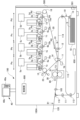
以下、図面を参照して本発明の実施形態を説明する。まず、本実施形態の画像形成装置の構成について、図1を用いて説明する。図1に示す画像形成装置100は、電子写真方式のタンデム型のフルカラープリンタである。画像形成装置100は、それぞれイエロー、マゼンタ、シアン、ブラックの画像を形成する画像形成部Pa、Pb、Pc、Pdを有する。画像形成装置100は、装置本体100Aに接続された原稿読取装置(不図示)又は装置本体100Aに対し通信可能に接続されたパーソナルコンピュータ等の外部機器(不図示)からの画像情報に応じてトナー像を記録材Sに形成する。記録材Sとしては、普通紙、厚紙、ラフ紙、凹凸紙、コート紙等の用紙、プラスチックフィルム、布など、といった様々な種類のシート材が挙げられる。
また、図1に示すように、画像形成装置100は制御部600を備えている。制御部600について、図1を参照しながら図2を用いて説明する。なお、制御部600には図示した以外にも、例えば一次転写電源75a~75d、一転電圧検出センサや一転電流検出センサ、また搬送経路(113、114)において記録材Sを搬送する各種ローラを駆動する各種モータなどの各種機器が接続されている。しかし、ここでは発明の本旨でないので、それらの図示及び説明を省略している。
そこで、制御部600は二転ATVC(Auto Transfer Voltage Control)制御を実行して、二次転写電圧を設定する。二転ATVC制御は、二次転写部T2を記録材Sが通過していないときに、二次転写部T2に目標電流を流すことが可能な電圧を基準電圧として設定する制御である。この基準電圧は、環境(例えば温湿度)の変動や長期使用による中間転写ベルト20や二次転写外ローラ11の電気抵抗の変化に応じて変わることから、制御部600は二転ATVC制御を実行して基準電圧を適宜に更新する。基準電圧は、メモリ602に記憶されている。制御部600は、例えば電源投入後の前回転時や、画像形成した記録材Sの累計枚数が所定枚数(例えば1000枚)を超えた後の紙間などに、二転ATVC制御を実行する。
ところで、記録材Sが例えば吸湿しやすい紙であるような場合には、記録材Sの種類が同じであっても、記録材Sの電気抵抗は吸湿状態によってつまりは記録材Sに含まれる水分量によって異なり得る。そのため、上記のように記録材Sの種類に応じた分担電圧を考慮した二次転写電圧を印加したにも関わらず、二次転写部T2に流れる電流が目標電流から外れ、中間転写ベルト20から記録材Sへの最適な二次転写が行えない虞がある。
図1に示すように、画像形成装置100として、装置本体100A内にカラーセンサ80(又はイメージスキャナ)が設けられた装置がある(図1参照)。その場合、制御部600は、出力モードの実行に伴い、カラーセンサ80(又はイメージスキャナ)の検出結果に基づいて二次転写電圧が自動的に設定(自動設定タイプ)される。以下、説明する。
b.等色関数x(λ)、y(λ)、z(λ)と標準光分光分布SD50(λ)を用意する。なお、等色関数はJIS Z8701で規定される。他方、SD50(λ)はJIS Z8720で規定され、補助標準イルミナントD50とも呼ばれる。
c.分光反射率R(λ)、等色関数x(λ),y(λ),z(λ)及び標準光分光分布SD50(λ)を波長毎に乗算する。
R(λ)×SD50(λ)×x(λ)
R(λ)×SD50(λ)×y(λ)
R(λ)×SD50(λ)×z(λ)
d.(c)の積を波長領域全体に亘って積算する。
Σ{R(λ)×SD50(λ)×x(λ)}
Σ{R(λ)×SD50(λ)×y(λ)}
Σ{R(λ)×SD50(λ)×z(λ)}
e.等色関数y(λ)と標準光分光分布SD50(λ)との積の積算値を求める。
Σ{SD50(λ)×y(λ)}
f.XYZ色空間における座標を算出する。
X=100×Σ{SD50(λ)×y(λ)}/Σ{R(λ)×SD50(λ)×x(λ)}
Y=100×Σ{SD50(λ)×y(λ)}/Σ{R(λ)×SD50(λ)×y(λ)}
Z=100×Σ{SD50(λ)×y(λ)}/Σ{R(λ)×SD50(λ)×z(λ)}
g.(f)で得られたXYZ座標をL*a*b*色空間に変換する。
L*=116×(Y/Yn)^(1/3)-16
a*=500{(X/Xn)^(1/3)-(Y/Yn)^(1/3)}
b*=200{(Y/Yn)^(1/3)-(Z/Zn)^(1/3)}
(X/Xn)^(1/3) → 7.78(X/Xn)^(1/3)+16/116
(Y/Yn)^(1/3) → 7.78(Y/Yn)^(1/3)+16/116
(Z/Zn)^(1/3) → 7.78(Z/Zn)^(1/3)+16/116
記録材とパッチ画像との色差=((記録材(L)-パッチ画像(L))^2+(記録材(a)-パッチ画像(a))^2+(記録材(b)-パッチ画像(b))^2)^0.2 ・・・ 式1
なお、画像形成装置100として、上記したカラーセンサ80の代わりにイメージスキャナが定着装置30の下流に設けられた装置がある。その場合、制御部600は、出力モードの実行に伴い、イメージスキャナの検出結果に基づいて二次転写電圧が自動的に設定される。イメージスキャナとしては、例えばCISタイプやCCDタイプのイメージスキャナが用いられ、例えばレッド、グリーン、ブルーに対応したフィルタを通して、調整用チャートに形成されたパッチ画像の光強度を検出可能である。また、イメージスキャナは、検出した光強度に基づき、上述したカラーセンサ80と同様に、パッチ画像の画像濃度と色度値(L*a*b*)を演算し得る。そして、制御部600(図2参照)はイメージスキャナから、グレーとブラックのパッチ画像に関しては画像濃度を取得し、ブルーのパッチ画像に関しては色度値(L*a*b*)を取得する。以降の処理についても、上述したカラーセンサ80と同様であることから、説明を省略する。
Claims (5)
- 像担持体にトナー像を形成する画像形成部と、
前記像担持体からトナー像が転写される中間転写体と、
前記中間転写体から記録材にトナー像を転写する転写部材と、
前記転写部材に電圧を印加する電源と、
前記転写部材に印可する転写電圧を調整するためのテストチャートであって、前記転写部材に異なる電圧を印加して複数のテストトナー像を前記中間転写体から複数の記録材に転写することで形成されるテストチャートを出力するモードを実行するように構成された制御部と、を備え、
前記制御部は、前記モード実行中にジャムが発生した場合は、前記ジャムの解消後に前記モードを自動的に再開可能に構成され、
前記制御部は、前記モード実行中において、前記テストチャートを出力する前に、前記テストチャート上に形成される複数のテストトナー像と同一条件で形成された複数のテストトナー像を記録材に出力することなく、前記テストチャートを出力するように構成され、前記ジャムが発生して前記モードを自動的に再開する場合は、前記ジャムにより排出されない前記複数の記録材の枚数に関わらず、前記複数の記録材の一枚目から出力するように構成されている、
ことを特徴とする画像形成装置。 - 記録材に転写されたトナーを定着する定着装置と、前記定着装置により記録材に定着された前記トナーに光を照射したときの反射光を検知する光センサと、を備え、前記制御部は、前記記録材に定着された前記複数のテストトナー像を前記光センサで検知したときの検知結果に基づいて、前記転写電圧を調整する、
ことを特徴とする請求項1記載の画像形成装置。 - 画面を表示する表示部を備え、前記制御部は、前記モード時において、前記転写電圧の設定を調整する調整値をユーザ入力させる画面を前記表示部に表示させるように構成され、入力された前記調整値に基づいて、前記転写電圧を設定するように構成されている、
ことを特徴とする請求項1記載の画像形成装置。 - 画像情報に基づいて複数の記録材に連続してトナー画像を形成する画像形成ジョブを実行中において、前記画像形成ジョブの二枚目の記録材でジャムが発生した場合は、前記複数の記録材の二枚目の記録材から前記画像形成ジョブを再開するように構成されている、
ことを特徴とする請求項1ないし3のいずれか1項に記載の画像形成装置。 - 前記複数のテストトナー像は、異なる色のトナーを重畳して形成された第1トナー像と、単色のトナーで形成された第2トナー像を含み、前記モードにおいて、前記制御部は、前記転写部材に異なる電圧を印加して、前記第1トナー像及び前記第2トナー像を前記複数の記録材に転写して前記テストチャートを形成する、
ことを特徴とする請求項1ないし4のいずれか1項に記載の画像形成装置。
Priority Applications (3)
| Application Number | Priority Date | Filing Date | Title |
|---|---|---|---|
| JP2020067875A JP7463173B2 (ja) | 2020-04-03 | 2020-04-03 | 画像形成装置 |
| US17/218,575 US11249422B2 (en) | 2020-04-03 | 2021-03-31 | Image forming apparatus |
| US17/582,772 US20220146968A1 (en) | 2020-04-03 | 2022-01-24 | Image forming apparatus |
Applications Claiming Priority (1)
| Application Number | Priority Date | Filing Date | Title |
|---|---|---|---|
| JP2020067875A JP7463173B2 (ja) | 2020-04-03 | 2020-04-03 | 画像形成装置 |
Publications (3)
| Publication Number | Publication Date |
|---|---|
| JP2021162824A JP2021162824A (ja) | 2021-10-11 |
| JP2021162824A5 JP2021162824A5 (ja) | 2023-03-27 |
| JP7463173B2 true JP7463173B2 (ja) | 2024-04-08 |
Family
ID=77922037
Family Applications (1)
| Application Number | Title | Priority Date | Filing Date |
|---|---|---|---|
| JP2020067875A Active JP7463173B2 (ja) | 2020-04-03 | 2020-04-03 | 画像形成装置 |
Country Status (2)
| Country | Link |
|---|---|
| US (2) | US11249422B2 (ja) |
| JP (1) | JP7463173B2 (ja) |
Citations (4)
| Publication number | Priority date | Publication date | Assignee | Title |
|---|---|---|---|---|
| JP2010072235A (ja) | 2008-09-17 | 2010-04-02 | Konica Minolta Business Technologies Inc | 画像形成装置 |
| JP2013037185A (ja) | 2011-08-08 | 2013-02-21 | Fuji Xerox Co Ltd | 画像形成装置及び画像形成システム |
| JP2013083861A (ja) | 2011-10-12 | 2013-05-09 | Canon Inc | 画像形成装置 |
| JP2019099291A (ja) | 2017-11-29 | 2019-06-24 | キヤノン株式会社 | 画像形成システム |
Family Cites Families (5)
| Publication number | Priority date | Publication date | Assignee | Title |
|---|---|---|---|---|
| JP2004280003A (ja) | 2003-03-19 | 2004-10-07 | Fuji Xerox Co Ltd | 画像形成装置、画像形成条件決定方法、プログラム |
| JP2005132049A (ja) | 2003-10-31 | 2005-05-26 | Canon Inc | 色度補正方法及びカラー画像形成装置 |
| JP6084007B2 (ja) * | 2011-12-22 | 2017-02-22 | キヤノン株式会社 | 画像形成装置、その方法およびプログラム |
| JP6628540B2 (ja) | 2015-10-06 | 2020-01-08 | キヤノン株式会社 | 画像形成装置 |
| JP7458862B2 (ja) * | 2020-04-03 | 2024-04-01 | キヤノン株式会社 | 画像形成装置 |
-
2020
- 2020-04-03 JP JP2020067875A patent/JP7463173B2/ja active Active
-
2021
- 2021-03-31 US US17/218,575 patent/US11249422B2/en active Active
-
2022
- 2022-01-24 US US17/582,772 patent/US20220146968A1/en not_active Abandoned
Patent Citations (4)
| Publication number | Priority date | Publication date | Assignee | Title |
|---|---|---|---|---|
| JP2010072235A (ja) | 2008-09-17 | 2010-04-02 | Konica Minolta Business Technologies Inc | 画像形成装置 |
| JP2013037185A (ja) | 2011-08-08 | 2013-02-21 | Fuji Xerox Co Ltd | 画像形成装置及び画像形成システム |
| JP2013083861A (ja) | 2011-10-12 | 2013-05-09 | Canon Inc | 画像形成装置 |
| JP2019099291A (ja) | 2017-11-29 | 2019-06-24 | キヤノン株式会社 | 画像形成システム |
Also Published As
| Publication number | Publication date |
|---|---|
| US20210311418A1 (en) | 2021-10-07 |
| US11249422B2 (en) | 2022-02-15 |
| JP2021162824A (ja) | 2021-10-11 |
| US20220146968A1 (en) | 2022-05-12 |
Similar Documents
| Publication | Publication Date | Title |
|---|---|---|
| JP6628540B2 (ja) | 画像形成装置 | |
| US8843003B2 (en) | Image forming apparatus, image forming system, and image forming method | |
| JP7458862B2 (ja) | 画像形成装置 | |
| CN111665702B (zh) | 图像形成装置 | |
| US11195068B2 (en) | Image forming apparatus | |
| US8983355B2 (en) | Image forming apparatus and image forming method | |
| US11308369B2 (en) | Image forming apparatus with mode for setting transfer voltage | |
| WO2021002410A1 (ja) | 画像形成装置 | |
| US20220308505A1 (en) | Image forming apparatus | |
| US20220197192A1 (en) | Image forming apparatus | |
| US20200050133A1 (en) | Image forming apparatus | |
| JP4820687B2 (ja) | カラー画像形成装置 | |
| JP7463173B2 (ja) | 画像形成装置 | |
| US11829088B2 (en) | Image forming apparatus using double-sided test chart | |
| JP2001083853A (ja) | 画像形成装置 | |
| JP4820686B2 (ja) | カラー画像形成装置 | |
| JP6135089B2 (ja) | 画像形成装置 | |
| US11726419B2 (en) | Image forming apparatus | |
| JP2000267458A (ja) | 画像形成装置 | |
| US10996591B2 (en) | Image forming apparatus | |
| JP2010181666A (ja) | カラー画像形成装置 | |
| US20200089146A1 (en) | Image forming apparatus | |
| JP2023118624A (ja) | 画像形成装置 | |
| JP2000231234A (ja) | 画像形成装置 | |
| JP2006018008A (ja) | 画像形成装置 |
Legal Events
| Date | Code | Title | Description |
|---|---|---|---|
| A521 | Request for written amendment filed |
Free format text: JAPANESE INTERMEDIATE CODE: A523 Effective date: 20230316 |
|
| A621 | Written request for application examination |
Free format text: JAPANESE INTERMEDIATE CODE: A621 Effective date: 20230316 |
|
| A977 | Report on retrieval |
Free format text: JAPANESE INTERMEDIATE CODE: A971007 Effective date: 20231206 |
|
| A131 | Notification of reasons for refusal |
Free format text: JAPANESE INTERMEDIATE CODE: A131 Effective date: 20231212 |
|
| A521 | Request for written amendment filed |
Free format text: JAPANESE INTERMEDIATE CODE: A523 Effective date: 20240207 |
|
| TRDD | Decision of grant or rejection written | ||
| A01 | Written decision to grant a patent or to grant a registration (utility model) |
Free format text: JAPANESE INTERMEDIATE CODE: A01 Effective date: 20240227 |
|
| A61 | First payment of annual fees (during grant procedure) |
Free format text: JAPANESE INTERMEDIATE CODE: A61 Effective date: 20240327 |
|
| R150 | Certificate of patent or registration of utility model |
Ref document number: 7463173 Country of ref document: JP Free format text: JAPANESE INTERMEDIATE CODE: R150 |