特許法第30条第2項適用 〔刊行物名〕 international ELECTRON DEVICES meeting 2018 TECHNICAL DIGEST, 312-315 発行年月日 平成30年12月1日 〔集会名〕 2018 IEEE International Electron Devices Meeting 開催日 平成30年12月1日-5日
以下に、本発明の実施の形態を説明する。ただし、本発明の一形態は、以下の説明に限定されず、本発明の趣旨およびその範囲から逸脱することなくその形態および詳細を様々に変更し得ることは、当業者であれば容易に理解される。したがって、本発明の一形態は、以下に示す実施の形態の記載内容に限定して解釈されるものではない。
なお本明細書等において、「第1」、「第2」、「第3」という序数詞は、構成要素の混同を避けるために付したものである。従って、構成要素の数を限定するものではない。また、構成要素の順序を限定するものではない。また例えば、本明細書等の実施の形態の一において「第1」に言及された構成要素が、他の実施の形態、あるいは特許請求の範囲において「第2」に言及された構成要素とすることもありうる。また例えば、本明細書等の実施の形態の一において「第1」に言及された構成要素を、他の実施の形態、あるいは特許請求の範囲において省略することもありうる。
図面において、同一の要素または同様な機能を有する要素、同一の材質の要素、あるいは同時に形成される要素等には同一の符号を付す場合があり、その繰り返しの説明は省略する場合がある。
本明細書において、例えば、電源電位VDDを、電位VDD、VDD等と省略して記載する場合がある。これは、他の構成要素(例えば、信号、電圧、回路、素子、電極、配線等)についても同様である。
また、複数の要素に同じ符号を用いる場合、特に、それらを区別する必要があるときには、符号に“_1”、”_2”、”[n]”、”[m,n]”等の識別用の符号を付記して記載する場合がある。例えば、2番目の配線GLを配線GL[2]と記載する。
(実施の形態1)
本発明の一態様である半導体装置、および半導体装置の動作方法の構成例について、図1乃至図5を参照して説明する。
なお半導体装置は半導体特性を利用した装置であり、半導体素子(トランジスタ、ダイオード、フォトダイオード等)を含む回路、同回路を有する装置である。本実施の形態で説明する半導体装置は、極小オフ電流のトランジスタを利用した記憶装置として機能する半導体装置として機能させることができる。
図1(A)は本実施の形態で説明する半導体装置のブロック図である。図1(A)に示す半導体装置10は、周辺回路20およびメモリセルアレイ30を有する。
周辺回路20は、ロウドライバ21およびカラムドライバ22を有する。ロウドライバ21およびカラムドライバ22は、単に駆動回路またはドライバという場合がある。
ロウドライバ21は、ワード線WLにメモリセルアレイ30を駆動するための信号を出力する機能を有する回路である。具体的にロウドライバ21は、ワード線WL(図1(A)ではWL_1およびWL_Nを図示。Nは2以上の自然数)にワード信号を伝える機能を有する。ロウドライバ21は、ワード線側駆動回路という場合がある。なおロウドライバ21は、指定されたアドレスに応じたワード線WLを選択するためのデコーダ回路、およびバッファ回路等を含む。なおワード線WLは、単に配線と呼ぶ場合がある。
カラムドライバ22は、ビット線BLにメモリセルアレイ30を駆動するための信号を出力する機能を有する回路である。具体的にカラムドライバ22は、ビット線BL(図1(A)ではBL_1およびBL_2)にデータ信号を伝える機能を有する。カラムドライバ22は、ビット線側駆動回路という場合がある。なおカラムドライバ22は、センスアンプ、プリチャージ回路、指定されたアドレスに応じたビット線を選択するためのデコーダ回路等を含む。なおビット線BLは、単に配線と呼ぶ場合がある。なお図面において、ビット線BLは、視認性を高めるため、太線あるいは太い点線等で図示する場合がある。
ビット線BLに与えられるデータ信号は、メモリセルに書き込まれる信号、またはメモリセルから読み出される信号に相当する。データ信号は、データ1又はデータ0に対応するハイレベル又はローレベルの電位を有する二値の信号として説明する。なおデータ信号は、3値以上の多値でもよい。ハイレベルの電位はVDD、ローレベルの電位はVSS、あるいはグラウンド電位(GND)である。ビット線BLに与えられる信号としては、データ信号の他、データを読み出すためのプリチャージ電位等がある。プリチャージ電位はVDD/2とすることができる。
メモリセルアレイ30は、複数、例えばN層(Nは2以上の自然数)の素子層34_1乃至34_Nを有する。素子層34_1は、1以上のメモリセル31_1を有する。メモリセル31_1は、トランジスタ32_1およびキャパシタ33_1を有する。素子層34_Nは、1以上のメモリセル31_Nを有する。メモリセル31_Nは、トランジスタ32_Nおよびキャパシタ33_Nを有する。なおキャパシタは、容量素子と呼ぶ場合がある。なお素子層は、キャパシタやトランジスタなどの素子が設けられる層であり、導電体、半導体、絶縁体等の部材で構成される層である。
トランジスタ32_1乃至32_Nは、ワード線WL_1乃至WL_Nに与えられるワード信号に応じてオンまたはオフが制御されるスイッチとして機能する。トランジスタ32_1乃至32_Nは、それぞれ、ソース又はドレインの一方が、ビット線BLのいずれか一(図中、BL_1)に接続される。
トランジスタ32_1乃至32_Nとして、チャネル形成領域に酸化物半導体を有するトランジスタ(以下、OSトランジスタという)で構成されることが好ましい。本発明の一態様の構成では、OSトランジスタを有するメモリセルを用いる構成とすることで、オフ時にソースとドレイン間を流れるリーク電流(以下、オフ電流)が極めて低い特性を利用して、所望の電圧に応じた電荷をソース又はドレインの他方にあるキャパシタ33_1乃至33_Nに保持させることができる。つまり、メモリセル31_1乃至31_Nにおいて、一旦書き込んだデータを長時間保持することができる。そのため、データリフレッシュの頻度を下げ、低消費電力化を図ることができる。
加えてOSトランジスタを用いたメモリセル31_1乃至31_Nでは、電荷の充電又は放電することによってデータの書き換えおよび読み出しが可能となるため、実質的に無制限回のデータの書き込みおよび読み出しが可能である。OSトランジスタを用いたメモリセル31_1乃至31_Nは、磁気メモリあるいは抵抗変化型メモリなどのように原子レベルでの構造変化を伴わないため、書き換え耐性に優れている。またOSトランジスタを用いたメモリセル31_1乃至31_Nは、フラッシュメモリのように繰り返し書き換え動作を行っても電子捕獲中心の増加による不安定性が認められない。
またOSトランジスタを用いたメモリセル31_1乃至31_Nは、チャネル形成領域にシリコンを含むトランジスタ(以下、Siトランジスタ)を有するシリコン基板上などに自由に配置可能であるため、集積化を容易に行うことができる。またOSトランジスタは、Siトランジスタと同様の製造装置を用いて作製することが可能であるため、低コストで作製可能である。
またOSトランジスタは、ゲート電極、ソース電極およびドレイン電極に加えて、バックゲート電極を含むと、4端子の半導体素子とすることができる。OSトランジスタは、ゲート電極またはバックゲート電極に与える電圧に応じて、ソースとドレインとの間を流れる信号の入出力が独立制御可能な電気回路網で構成することができる。そのため、LSIと同一思考で回路設計を行うことができる。加えてOSトランジスタは、高温環境下において、Siトランジスタよりも優れた電気特性を有する。具体的には、125℃以上150℃以下といった高温下においてもオン電流とオフ電流の比が大きいため、良好なスイッチング動作を行うことができる。
なお図1(A)に示すメモリセルは、OSトランジスタをメモリに用いたDOSRAM(Dynamic Oxide Semiconductor Random Access Memory)と呼ぶことができる。一つのトランジスタ、及び一つの容量で構成することができるため、メモリの高密度化を実現できる。また、OSトランジスタを用いることで、データの保持期間を長くすることができる。キャパシタ33_1乃至33_Nは、電極となる導電体の間に絶縁体を挟んだ構成となる。なお電極を構成する導電体としては、金属の他、導電性を付与した半導体層などを用いることができる。また詳細は後述するが、キャパシタ33_1乃至33_Nをトランジスタ32_1乃至32_Nの上方または下方の重なる位置に配置する他、トランジスタ32_1乃至32_Nを構成する半導体層あるいは電極等の一部をキャパシタ33_1乃至33_Nの一方の電極として用いることができる。
図1(A)で説明した各構成において、本発明の一態様にある素子層34_1乃至34_Nについて説明するため、図1(B)に図示する模式図を用いて説明する。図1(B)に示す模式図は、図1(A)で説明した各構成の配置を説明するため、x軸、y軸、z軸方向を規定した斜視図に対応する。なお理解を容易にするため、明細書中、x軸方向を奥行き方向、y軸方向を水平方向、z軸方向を垂直方向と呼ぶ場合がある。
図1(B)に図示するように素子層34_1乃至34_Nは、N層で積層して設けられる。メモリセル31_1乃至31_Nを有する素子層34_1乃至34_Nは、それぞれシリコン基板11に設けられたカラムドライバ22と重なる領域を有する。図1(B)に図示するように素子層34_1は、シリコン基板11と素子層34_Nとの間に設けられるともいえる。
また素子層34_1が有するメモリセル31_1のトランジスタと、素子層34_Nが有するメモリセル31_Nのトランジスタと、は、垂直方向に設けられたビット線BLを介して接続される。またビット線BLは、シリコン基板11に設けられたカラムドライバ22に接続される。
ビット線BL_1は、メモリセル31_1が有するトランジスタの半導体層およびメモリセル31_Nが有するトランジスタの半導体層に接して設けられる。あるいはビット線BL_1は、メモリセル31_1が有するトランジスタの半導体層のソースまたはドレインとして機能する領域、およびメモリセル31_Nが有するトランジスタの半導体層のソースまたはドレインとして機能する領域、に接して設けられる。あるいはビット線BL_1は、メモリセル31_1が有するトランジスタの半導体層のソースまたはドレインとして機能する領域と接して設けられる導電体、およびメモリセル31_Nが有するトランジスタの半導体層のソースまたはドレインとして機能する領域と接して設けられる導電体、に接して設けられる。つまりビット線BLは、メモリセル31_1が有するトランジスタのソース又はドレインの一方と、メモリセル31_Nが有するトランジスタのソース又はドレインの一方と、カラムドライバ22と、を垂直方向で電気的にするための配線であるといえる。
なおビット線BLは、カラムドライバ22が設けられるシリコン基板11の面に垂直方向または概略垂直方向に延びて設けられるということができる。つまり図1(B)に図示するようにビット線BLは、メモリセル31_1が有するトランジスタおよびメモリセル31_Nが有するトランジスタに接続され、且つ前記シリコン基板の表面(xy平面)に対して垂直方向または概略垂直方向’(z方向)に設けられる。なお「概略垂直」とは、85度以上95度以下の角度で配置されている状態をいう。
なおシリコン基板11に設けられたロウドライバ21と、素子層34_1乃至素子層34_Nの奥行き方向に延びて設けられるワード線WLとは、素子層34_1乃至素子層34_Nにおけるメモリセル31_1乃至31_Nが設けられていない領域、例えば素子層34_1乃至素子層34_Nの外周部における開口部を介して接続する構成とすればよい。シリコン基板11に設けられたロウドライバ21と、各素子層に設けられたワード線WLと、の接続は、素子層34_1乃至素子層34_Nの上層に設けられる配線を介して行ってもよい。
本発明の一形態は、各素子層に設けられるトランジスタとして、オフ電流が極めて低いOSトランジスタを用いる。そのため、メモリセルに保持するデータのリフレッシュ頻度を低減することができ、低消費電力化が図られた半導体装置とすることができる。OSトランジスタは、積層して設けることができ、垂直方向に繰り返し同じ製造工程を用いて作製することができ、製造コストの低減を図ることができる。また本発明の一形態は、メモリセルを構成するトランジスタを平面方向でなく、垂直方向に配置してメモリ密度の向上を図ることができ、装置の小型化を図ることができる。またOSトランジスタは、高温環境下においてもSiトランジスタと比べて電気特性の変動が小さいため、積層且つ集積化した際のトランジスタの電気特性の変動が小さく信頼性に優れた記憶装置として機能する半導体装置とすることができる。また本発明の一態様は、メモリセルアレイから延びて設けられるビット線を垂直方向に設けることで、メモリセルアレイとカラムドライバとのビット線の長さを短くできる。そのため、ビット線の寄生容量を大幅に削減できるため、メモリセルに保持するデータ信号を多値化しても電位を読み出すことができる。
図2では、図1(A)および図1(B)を用いて説明した半導体装置10の垂直方向(z軸方向)に平行な面の断面の模式図について示す。
図2に図示するように半導体装置10は、各層の素子層に設けられたメモリセル31_1乃至31_Nと、シリコン基板11に設けられるカラムドライバ22と、を最短距離である垂直方向に設けられるビット線BLを介して接続する構成とすることができる。ビット線BLを平面方向に配置する構成と比べて、ビット線BLの本数が増えるものの、1本のビット線に接続されるメモリセル31_1乃至31_Nの数を少なくすることができるため、ビット線BLの寄生容量を小さくできる。そのため、メモリセル31_1乃至31_Nが有するキャパシタ33_1乃至33_Nの容量を小さくしても、電荷の移動に伴うビット線BLの電位を変動させることができる。
またメモリセル31_1乃至31_Nが有するキャパシタ33_1乃至33_Nの容量を小さくすることができるため、キャパシタ33_1乃至33_Nをトランジスタ32_1乃至32_Nと同じ層に設けることができる。キャパシタ33_1乃至33_Nをトランジスタ32_1乃至32_Nと同じ層に設ける構成とすることで、一層毎の素子層34_1乃至34_Nを薄くすることができる。そのため、半導体装置10の小型化を図ることができる。
なおメモリセル31_1乃至31_Nが有するキャパシタ33_1乃至33_Nは、トランジスタ32_1乃至32_Nと同じ層に設ける構成でもよいが、他の構成でもよい。例えば、図3(A)に示す模式図では、素子層34_1乃至34_Nが有するメモリセル31のキャパシタ33Aがトランジスタ32に対して、垂直方向で上方に設けられる構成を表している。当該構成とすることで、容量を大きくすることができるため、読み出されるデータの信頼性、データの保持時間の向上を図ることができる。加えて図3(A)の構成ではトランジスタ32の上方に固定電位に一方の電極が接続されたキャパシタ33Aの電極を配置することができるため、外部からのノイズの影響を抑制することができる。
また図3(B)に示す模式図は、素子層34_1乃至34_Nが有するメモリセル31のキャパシタ33Bがトランジスタ32に対して、垂直方向で下方に設けられる構成を表している。当該構成とすることで、容量を大きくすることができるため、読み出されるデータの信頼性、データの保持時間の向上を図ることができる。加えて図3(B)の構成ではトランジスタ32と、カラムドライバ22と、の間に固定電位に一方の電極が接続されたキャパシタ33Bの電極を配置することができるため、カラムドライバ22のノイズのメモリセル31への影響を抑制することができる。
図4は、図1(A)で説明した、素子層34_1乃至34_Nを有するメモリセルアレイ30の回路構成例と、当該メモリセルに接続されるカラムドライバ22の具体的な回路構成例と、について説明する回路図である。
図4にはメモリセルアレイ30として素子層34_1乃至34_Nを図示している。図4では、ビット線BL_Aに接続されたメモリセルとしてメモリセル31_N_Aを図示している。メモリセル31_N_Aは、ゲートがワード線WL_Aに接続されたトランジスタ32Aとキャパシタ33を有している。また図4では、ビット線BL_Bに接続されたメモリセルとしてメモリセル31_N_Bを図示している。メモリセル31_N_Bは、ゲートがワード線WL_Bに接続されたトランジスタ32Bとキャパシタ33を有している。各素子層のキャパシタ33は、固定電位、例えばグラウンド電位が与えられる配線VLに接続される。
また図4には、カラムドライバ22が有する回路として、シリコン基板側にあるプリチャージ回路22_1、センスアンプ22_2、選択スイッチ22_3、書き込み読み出し回路29を示している。プリチャージ回路22_1およびセンスアンプ22_2を構成するトランジスタは、Siトランジスタを用いる。選択スイッチ22_3についてもSiトランジスタを用いることができる。
プリチャージ回路22_1は、nチャネル型のトランジスタ24_1乃至24_3で構成される。プリチャージ回路22_1は、プリチャージ線PCLに与えられるプリチャージ信号に応じて、ビット線BL_Aおよびビット線BL_BをVDDとVSSの間の電位VDD/2に相当する中間電位VPCにプリチャージするための回路である。
センスアンプ22_2は、配線VHHまたは配線VLLに接続された、pチャネル型のトランジスタ25_1、25_2およびnチャネル型のトランジスタ25_3、25_4で構成される。配線VHHまたは配線VLLは、VDD又はVSSを与える機能を有する配線である。トランジスタ25_1乃至25_4は、インバータループを構成するトランジスタである。センスアンプ22_2は、ワード線WL_A、WL_Bをハイレベルとしてメモリセル31_N_A、31_N_Bを選択することで変化するビット線BL_Aおよびビット線BL_Bの電位を高電源電位VDDまたは低電源電位VSSにする。ビット線BL_Aおよびビット線BL_Bの電位は、書き込み読み出し回路29を介して外部に出力することができる。ビット線BL_Aおよびビット線BL_Bは、ビット線対に相当する。
また図5では、図4に示す回路図の動作を説明するためのタイミングチャートを示す。図5に示すタイミングチャートにおいて、期間T1は初期化の動作、期間T2は書き込みの動作、期間T3は非アクセス時の動作、期間T4は読み出しの動作を説明する期間に対応する。なお図5の説明では、選択スイッチ22_3が有するスイッチ23_A、23_Bの説明を省略するが、書き込みの動作、および読み出しの動作時において、適宜オンとなるよう選択される。
図5において、波形間に付された矢印は、動作の理解を容易にするためのものである。信号線のうち、配線PCLの高レベル(Hレベル)はVDDである。WLの高レベルはVHM(>VDD)であるが、VDDとしてもよい。
期間T1では、配線VPC、配線VHHおよび配線VLLはVDD/2とされる。ビット線BL_Aはプリチャージされ、VDD/2とする。ビット線BL_Aのプリチャージはプリチャージ回路22_1によって行われる。配線PCLを高レベル(Hレベル)にすることで、ビット線BL_A(あるいはビット線BL_B)のプリチャージと電位の平滑化が行われる。
期間T2では、書き込みアクセスがあると、ビット線BL_A(あるいはビット線BL_B)をプリチャージ状態から浮遊状態にする。これは配線PCLをHレベルからLレベルにすることで行われる。ワード線WL_AをHレベルにする。WL_Aが選択された後、VHHはVDDとされ、VLLはGNDとされる。トランジスタ32Aがオンになることで、ビット線BL_AにデータDA1が書き込まれる。ワード線WL_AをLレベルにした後、ビット線BL_A(あるいはビット線BL_B)のプリチャージ動作を開始し、これらをVDD/2にプリチャージしている。
期間T3では、配線PCLはHレベルであり、ワード線WL_AはLレベルである。VPC、VHHおよびVLLはVDD/2である。ビット線対およびローカルビット線対はVDD/2にプリチャージされている。VHH、VLLをVDD/2にしておくことで、センスアンプ22_2のリーク電流を低減することができる。
期間T4では、読み出しアクセスがあると、ビット線BL_A(あるいはビット線BL_B)をプリチャージ状態から浮遊状態にする。次に、ワード線WL_AをHレベルにして、トランジスタ32Aをオンにする。ビット線BL_Aには、データDA1が書き込まれることとなる。ワード線WL_AをHレベルした後、VHHをVDDにし、かつVLLをGNDにし、センスアンプ22_2を差動増幅回路として機能させ、ビット線BL_AのデータDA1を増幅する。ビット線BL_AのデータDA1は書き込み読み出し回路29によって読み出される。
本発明の一形態の半導体装置は、各素子層に設けられるトランジスタとして、オフ電流が極めて低いOSトランジスタを用いる。OSトランジスタは、Siトランジスタが設けられるシリコン基板上に積層して設けることができる。そのため、垂直方向に繰り返し同じ製造工程を用いて作製することができ、製造コストの低減を図ることができる。また本発明の一形態は、メモリセルを構成するトランジスタを平面方向でなく、垂直方向に配置してメモリ密度の向上を図ることができ、装置の小型化を図ることができる。
(実施の形態2)
本発明の一態様である半導体装置の構成例について、図6乃至図10を参照して説明する。実施の形態1と同じ符号を付した構成については、実施の形態1の説明を援用し、説明を省略する場合がある。
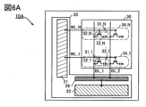
図6(A)には、半導体装置10Aのブロック図を示す。
周辺回路20は、ロウドライバ21、カラムドライバ22および切り替え回路が設けられる素子層26を有する。切り替え回路は、単に駆動回路という場合がある。切り替え回路は、メモリセルと、カラムドライバと、の間の導通状態を制御する機能を有するトランジスタを有する。
切り替え回路が設けられる素子層26は、カラムドライバ22をビット線BLに選択的に接続する機能を有する。切り替え回路は、カラムドライバ22から出力される選択信号に応じて、所定のビット線とカラムドライバ22のセンスアンプなどの駆動回路とを接続するマルチプレクサとしての機能を有する。切り替え回路は、切り替え回路で選択されたビット線BLにメモリセルアレイ30を駆動するための信号を出力する機能を有する回路である。
図6(A)の半導体装置において、切り替え回路が設けられる素子層26は、垂直方向において、カラムドライバ22に接続されたビット線BLの本数を低減し、データの書き込み時間の短縮、読み出し精度の向上を図ることができる。
また切り替え回路を構成するトランジスタは、OSトランジスタであることが好ましい。OSトランジスタを用いた切り替え回路を有する素子層26は、Siトランジスタを用いた回路上などに自由に配置可能であるため、集積化を容易に行うことができる。またOSトランジスタは、Siトランジスタと同様の製造装置を用いて作製することが可能であるため、低コストで作製可能である。
図6(A)で説明した各構成において、本発明の一態様にある素子層34_1乃至34_Nおよび切り替え回路を有する素子層26について説明するため、図6(B)に図示する模式図を用いて説明する。図6(B)に示す模式図は、図6(A)で説明した各構成の配置を説明するため、x軸、y軸、z軸方向を規定した斜視図に対応する。
図6(B)に図示するように半導体装置10Aにおいて、切り替え回路を構成するトランジスタが設けられる素子層26がV層(Vは1以上の自然数)、素子層34_1乃至素子層34_NがN層あり、合計(N+V)層のOSトランジスタを有する層がシリコン基板11上に積層して設けられる。素子層34_1乃至素子層34_Nが有するメモリセル31_1乃至31_N、および切り替え回路を構成するトランジスタが設けられる素子層26は、それぞれシリコン基板11に設けられたカラムドライバ22と重なる領域を有する。図6(B)に図示するように素子層26は、シリコン基板11と素子層34_1との間に設けられるともいえる。また図6(B)に図示するように素子層34_1は、シリコン基板11と素子層34_Nとの間に設けられるともいえる。
また素子層34_1が有するメモリセル31_1のトランジスタと、素子層34_Nが有するメモリセル31_Nのトランジスタと、は、垂直方向に設けられたビット線BLを介して接続される。またビット線BLは、切り替え回路を構成するトランジスタが設けられる素子層26に接続される。素子層26は、シリコン基板11に設けられたカラムドライバ22に接続される。
ビット線BL_1は、メモリセル31_1が有するトランジスタの半導体層に接して設けられる。あるいはビット線BL_1は、メモリセル31_1が有するトランジスタの半導体層のソースまたはドレインとして機能する領域に接して設けられる。あるいはビット線BL_1は、メモリセル31_1が有するトランジスタの半導体層のソースまたはドレインとして機能する領域と接して設けられる導電体に接して設けられる。つまりビット線BLは、メモリセル31_1が有するトランジスタのソース又はドレインの一方と、メモリセル31_Nが有するトランジスタのソース又はドレインの一方と、素子層26と、を垂直方向で電気的にするための配線であるといえる。
本発明の一形態は、各素子層に設けられるトランジスタとして、オフ電流が極めて低いOSトランジスタを用いる。そのため、メモリセルに保持するデータのリフレッシュ頻度を低減することができ、低消費電力化が図られた半導体装置とすることができる。OSトランジスタは、積層して設けることができ、垂直方向に繰り返し同じ製造工程を用いて作製することができ、製造コストの低減を図ることができる。また本発明の一形態は、メモリセルを構成するトランジスタを平面方向でなく、垂直方向に配置してメモリ密度の向上を図ることができ、装置の小型化を図ることができる。またOSトランジスタは、高温環境下においてもSiトランジスタと比べて電気特性の変動が小さいため、積層且つ集積化した際のトランジスタの電気特性の変動が小さく信頼性に優れた記憶装置として機能する半導体装置とすることができる。
加えて本発明の一形態は切り替え回路を有する素子層を備えている。切り替え回路は、カラムドライバが有するセンスアンプに接続されたビット線BLの本数を低減することができる。そのため、ビット線BLの負荷を低減することができる。切り替え回路は、垂直方向において、カラムドライバに接続されたビット線BLの本数を低減し、データの書き込み時間の短縮、読み出し精度の向上を図ることができる。また、不要なビット線を充放電することを避けることができ、低消費電力化が図られた半導体装置とすることができる。センスアンプ等の回路の直上にメモリセルを配置することが可能なため、半導体装置の小型化を図ることができる。またメモリセルが有するキャパシタの容量を小さくしても動作させることが可能となる。また本発明の一態様は、メモリセルアレイから延びて設けられるビット線を垂直方向に設けることで、メモリセルアレイとカラムドライバとのビット線の長さを短くできる。そのため、ビット線の寄生容量を大幅に削減できるため、メモリセルに保持するデータ信号の多値化しても電位を読み出すことができる。
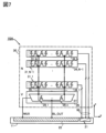
図7では、図6(A)および図6(B)を用いて説明した半導体装置10Aの垂直方向(z軸方向)に平行な面の断面の模式図について示す。
図7に図示するように半導体装置10Aは、各層の素子層に設けられたメモリセル31_1乃至31_Nと、素子層26と、シリコン基板11に設けられるカラムドライバ22と、を最短距離である垂直方向に設けられるビット線BLを介して接続する構成とすることができる。切り替え回路27を有する素子層26の数が増えるものの、カラムドライバ22が有するセンスアンプに接続されたビット線BLの本数を低減することができる。そのため、ビット線BLの負荷を低減することができる。
また図7に図示するように切り替え回路27が有するトランジスタ28_1乃至28_n(nは2以上の自然数)は、カラムドライバ22から出力される選択信号MUXに応じて選択されたビット線BLの電位を信号BL_OUTとしてカラムドライバ22に出力することができる。なお図7に示す半導体装置10Aは、ユニット30_1として表すことができる。
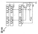
図8には、メモリセルアレイ30として素子層34_1乃至34_Nの他、トランジスタ28_a、28_bを有する素子層26を加えた回路図を図示している。図8に図示するトランジスタ28_a、28_bを有する素子層26上には、素子層34_1乃至34_Nが設けられ、ビット線BL_AおよびBL_Bが垂直方向に設けられる。つまり周辺回路の一部を構成する切り替え回路を有する素子層は、素子層34_1乃至34_Nと同様に積層して設けることができる。ビット線BL_AおよびBL_Bは、トランジスタ28_a、28_bのソース又はドレインの一方に接続される。
また図8には、カラムドライバ22が有する回路として、シリコン基板側にあるプリチャージ回路22_1、センスアンプ22_2、スイッチ回路22_3、および書き込み読み出し回路29を示している。プリチャージ回路22_1およびセンスアンプ22_2を構成するトランジスタは、Siトランジスタを用いる。選択スイッチ22_3についてもSiトランジスタを用いることができる。トランジスタ28_a、28_bのソース又はドレインの他方は、プリチャージ回路22_1およびセンスアンプ22_2を構成するトランジスタに接続される。また図8では、スイッチ回路22_3が有するスイッチ回路23_Aに接続される配線に接続される素子層34_1乃至34_N、および素子層26を表すブロックの他、スイッチ回路22_3が有するスイッチ回路23_Bに接続される配線に接続される素子層34_1乃至34_N、および素子層26を表すブロックを図示している。
切り替え回路を有する素子層26では、ビット線BL_AまたはBL_Bを選択して、プリチャージ回路22_1およびセンスアンプ22_2に接続される一対の配線の一方、およびスイッチ23_Aに接続される。またもう一対の切り替え回路を有する素子層26でも、ビット線BLを選択して、プリチャージ回路22_1およびセンスアンプ22_2に接続される一対の配線の他方、およびスイッチ23_Bに接続される。選択されたビット線に接続された、メモリセルのワード線をハイレベルとして選択することでプリチャージされたビット線の電位が変化し、当該変化に応じてプリチャージ回路22_1およびセンスアンプ22_2に接続された一対の配線の電位が高電源電位VDDまたは低電源電位VSSとなる。当該電位は、スイッチ回路22_3および書き込み読み出し回路29を介して外部に出力することができる。
図8に図示するように半導体装置10Aは、切り替え回路を有する素子層26の数が増えるものの、複数のビット線BLのいずれか一を選択して、カラムドライバ22に接続することができる。そのため、少ない本数のビット線BLをセンスアンプ22_2に接続する構成とすることができ、ビット線BLの負荷を低減することができる。
なお図7で図示した半導体装置10Aにおけるユニット30_1は、垂直方向に積層して設ける構成とすることができる。図9には、図7で説明したユニット30_1をM段(ユニット30_1乃至30_M、Mは2以上)積層した構成の半導体装置10Aを図示する。図9は、半導体装置の垂直方向(z軸方向)に平行な面の断面の模式図に相当する。つまり図9に示す半導体装置10Aの構成は、図7で図示した素子層の積層を、合計M×(N+V)層とした構成である。
図9に図示するように半導体装置10Aは、ユニット30_1乃至30_Mにおいて、それぞれ切り替え回路27_1乃至27_Mを備える。切り替え回路27_1乃至27_Mは、選択信号MUXが入力されることで信号BL_OUTを出力する。信号BL_OUTが出力される複数の配線のいずれか一は、選択信号SELで切り替え可能なスイッチ回路98で選択され、ビット線BLとは異なる配線GBLを介してカラムドライバ22に接続される。なおスイッチ回路98は、切り替え回路27_1乃至27_Mを構成するOSトランジスタを用いることができる。
当該構成とすることで、ユニット30_1乃至30_Mそれぞれの素子層34_1乃至34_Nの積層数を削減することができる。そのため、ユニット30_1乃至30_Mそれぞれのビット線BLの長さを短くすることができ、ビット線BLの負荷を低減することができる。なお図面において、配線GBLは、視認性を高めるため、太線あるいは太い点線等で図示する場合がある。配線GBLは、グローバルビット線と呼ぶ場合がある。
なお図9に示す配線GBLは、OSトランジスタを有する素子層を作製した後に、設けることが可能である。例えば、図10(A)に図示する断面図の模式図のように、OSトランジスタを有する素子層を作製し、各素子層を取り囲む封止層70Aの外周に開口を設けて、当該開口に配線GBLを設けることができる。あるいは、図10(A)に図示する断面図の模式図のように、OSトランジスタを有する素子層を作製し、各素子層を一括して取り囲む封止層70Bの外周に開口を設けて、当該開口に配線GBLを設けることができる。なお配線GBLを備えた各素子層の詳細については、実施の形態3で詳述する。
本発明の一形態の半導体装置は、各素子層に設けられるトランジスタとして、オフ電流が極めて低いOSトランジスタを用いる。OSトランジスタは、Siトランジスタが設けられるシリコン基板上に積層して設けることができる。そのため、垂直方向に繰り返し同じ製造工程を用いて作製することができ、製造コストの低減を図ることができる。また本発明の一形態は、メモリセルを構成するトランジスタを平面方向でなく、垂直方向に配置してメモリ密度の向上を図ることができ、装置の小型化を図ることができる。
加えて本発明の一形態は、切り替え回路を有する素子層を備えている。切り替え回路は、垂直方向において、カラムドライバに接続されたビット線BLの本数を低減し、データの書き込み時間の短縮、読み出し精度の向上を図ることができる。また、不要なビット線を充放電することを避けることができ、低消費電力化が図られた半導体装置とすることができる。
(実施の形態3)
本発明の一態様である半導体装置の構成例について、図11乃至図24を参照して説明する。実施の形態1と同じ符号を付した構成については、実施の形態1の説明を援用し、説明を省略する場合がある。
図11(A)には、半導体装置10Bのブロック図を示す。
周辺回路20は、ロウドライバ21と、カラムドライバ22と、制御回路が設けられる素子層40と、を有する。制御回路は、OSトランジスタで構成されるセンスアンプとして機能する回路を有する。
制御回路が設けられる素子層40は、OSトランジスタで構成されるセンスアンプとして機能する回路を有する。OSトランジスタで構成されるセンスアンプは、各メモリセルへのデータ信号の書き込みまたは読み出しの他、メモリセル31_1乃至31_Nを含むユニット50_1乃至50_Mを選択するための切り替え回路として機能する。素子層40には、カラムドライバ22からOSトランジスタで構成されるセンスアンプを駆動するための制御信号WE,RE,MUXが与えられる。センスアンプとして機能する回路は、メモリセルへのデータ信号の読み出しまたは書き込みを制御するためのトランジスタを有するため、制御回路という場合がある。
図11(A)の半導体装置において、制御回路は、増幅器として機能させることができる。当該構成にすることで、読み出し時にビット線BLのわずかな電位差を増幅して、Siトランジスタを用いたセンスアンプを駆動することができる。
また制御回路を構成するトランジスタは、OSトランジスタであることが好ましい。OSトランジスタを用いた制御回路を有する素子層40は、Siトランジスタを用いた回路上などに自由に配置可能であるため、集積化を容易に行うことができる。またOSトランジスタは、Siトランジスタと同様の製造装置を用いて作製することが可能であるため、低コストで作製可能である。
図11(A)で説明した各構成において、本発明の一態様にある素子層34_1乃至34_Nおよび制御回路を有する素子層40について説明するため、図11(B)に図示する模式図を用いて説明する。図11(B)に示す模式図は、図11(A)で説明した各構成の配置を説明するため、x軸、y軸、z軸方向を規定した斜視図に対応する。
図11(B)に図示するように半導体装置10Bにおいて、制御回路を構成するトランジスタが設けられる素子層40がV層(Vは1以上の自然数)、素子層34_1乃至素子層34_NがN層あり、合計(N+V)層のOSトランジスタを有する層がシリコン基板11上に積層して設けられる。素子層34_1乃至素子層34_Nが有するメモリセル31_1乃至31_N、および制御回路を構成するトランジスタが設けられる素子層40は、それぞれシリコン基板11に設けられたカラムドライバ22と重なる領域を有する。図11(B)に図示するように素子層40は、シリコン基板11と素子層34_1との間に設けられるともいえる。また図11(B)に図示するように素子層34_1は、シリコン基板11と素子層34_Nとの間に設けられるともいえる。
また素子層34_1が有するメモリセル31_1のトランジスタと、素子層34_Nが有するメモリセル31_Nのトランジスタと、は、垂直方向に設けられたビット線BLを介して接続される。またビット線BLは、制御回路を構成するトランジスタが設けられる素子層40に接続される。素子層40は、ビット線BLとは別に設けられた配線GBL(図示せず)を介して、シリコン基板11に設けられたカラムドライバ22に接続される。なお図面において、配線GBLは、視認性を高めるため、太線あるいは太い点線等で図示する場合がある。
ビット線BL_1は、メモリセル31_1が有するトランジスタの半導体層に接して設けられる。あるいはビット線BL_1は、メモリセル31_1が有するトランジスタの半導体層のソースまたはドレインとして機能する領域に接して設けられる。あるいはビット線BL_1は、メモリセル31_1が有するトランジスタの半導体層のソースまたはドレインとして機能する領域と接して設けられる導電体に接して設けられる。つまりビット線BLは、メモリセル31_1が有するトランジスタのソースまたはドレインの一方と、メモリセル31_Nが有するトランジスタのソースまたはドレインの一方と、素子層40と、を垂直方向で電気的にするための配線であるといえる。
半導体装置10Bは、1種類のメモリセルを有しているが、2種類以上のメモリセルを有していてもよい。図12(A)は、半導体装置10Cの構成例を示すブロック図であり、半導体装置10Bの変形例である。半導体装置10Cは、メモリセルアレイ30にメモリセル31の他、メモリセル31と異なる構成であるメモリセル51が設けられる点が半導体装置10Bと異なる。半導体装置10Cは、1以上のメモリセル51により構成されている素子層54を有する。
半導体装置10Cにおいて、素子層54は素子層34_i(iは1以上N-1以下の整数)と素子層34_i+1との間に設けることができる。なお、素子層54は2層以上設けられていてもよい。半導体装置10Cが素子層54を2層以上有する場合、例えば第1の素子層54と第2の素子層との間には素子層34が設けられていてもよいし、設けられていなくてもよい。
半導体装置10Cでは、ロウドライバ21はワード線WL2を介してメモリセル51と電気的に接続されている。半導体装置10Cが有するロウドライバ21は、ワード線WLの他、ワード線WL2にメモリセルアレイ30を駆動するための信号を出力する機能を有する。具体的にロウドライバ21は、ワード線WLだけでなく、ワード線WL2にワード信号を伝える機能を有する。なお、ワード線WL2にワード信号を伝える機能を有するロウドライバを、ワード線WLにワード信号を伝える機能を有するロウドライバとは別に設けてもよい。また、ワード線WL2は、単に配線と呼ぶ場合がある。
図12(B)は、メモリセル51の構成例を示す回路図である。メモリセル51は、トランジスタ55と、トランジスタ56と、容量素子57と、を有する。
トランジスタ55のソースまたはドレインの一方は、トランジスタ56のゲートと電気的に接続されている。トランジスタ56のゲートは、容量素子57の一方の電極と電気的に接続されている。トランジスタ55のソースまたはドレインの他方、およびトランジスタ56のソースまたはドレインの一方は、配線BLと電気的に接続されている。トランジスタ56のソースまたはドレインの他方は、配線SLと電気的に接続されている。容量素子57の他方の電極は、配線CALと電気的に接続されている。ここで、トランジスタ55のソースまたはドレインの一方と、トランジスタ56のゲートと、容量素子57の一方の電極と、が電気的に接続されるノードをノードNとする。
配線CALは、容量素子57の他方の電極に所定の電位を印加するための配線としての機能を有する。メモリセル51からデータを読み出す際の配線CALの電位を、メモリセル51にデータを書き込む際、およびメモリセル51にデータを保持している最中の配線CALの電位と異ならせる。これにより、メモリセル51からデータを読み出す際のトランジスタ56の見かけのしきい値電圧を、メモリセル51にデータを書き込む際、およびメモリセル51にデータを保持している最中のトランジスタ56の見かけのしきい値電圧と異ならせることができる。
メモリセル51が図12(B)に示す構成である場合、メモリセル51にデータを書き込む際、およびメモリセル51にデータを保持している最中は、メモリセル51に書き込まれたデータによらず、配線SLと配線BLとの間に電流が流れない。一方、メモリセル51からデータを読み出す際は、配線SLと配線BLとの間に、メモリセル51に保持されたデータに対応する電流が流れる。
トランジスタ55は、OSトランジスタとすることが好ましい。前述のように、OSトランジスタはオフ電流が極めて低い。よって、メモリセル51に書き込まれたデータに対応する電荷を、ノードNに長時間保持させることができる。つまり、メモリセル51において、一旦書き込んだデータを長時間保持することができる。そのため、データリフレッシュの頻度を下げ、本発明の一態様の半導体装置の消費電力を低減させることができる。
またOSトランジスタを用いたメモリセル51は、シリコン基板上などに自由に配置可能であるため、集積化を容易に行うことができる。なお、メモリセル51の集積化の観点から、トランジスタ56をOSトランジスタとすることが好ましい。
トランジスタ55は、バックゲート電極を有することが好ましい。バックゲート電極に印加する電位を制御することで、トランジスタ55のしきい値電圧を制御することができる。これにより、例えばトランジスタ55のオン電流を大きくし、オフ電流を小さくすることができる。なお、トランジスタ56がOSトランジスタである場合は、トランジスタ56にもバックゲート電極を設けることが好ましい。
図12(B)に示す構成のメモリセル51は、OSトランジスタをメモリに用いたNOSRAM(Nonvolatile Oxide Semiconductor RAM)と呼ぶことができる。NOSRAMは、非破壊読み出しを行うことができるという特徴を有する。一方、メモリセル31に適用することができるDOSRAMは、保持されたデータを読み出す際は破壊読み出しを行う。
半導体装置10Cの動作について説明する。カラムドライバ22からメモリセルアレイ30に書き込まれるデータは、メモリセル31に保持される。メモリセル31に保持されたデータのうち、読み出し頻度が高いデータは、メモリセル31からメモリセル51に書き移す。前述のように、NOSRAMであるメモリセル51は非破壊読み出しを行うことができるので、データリフレッシュの頻度を下げることができる。よって、本発明の一態様の半導体装置の消費電力を低減させることができる。
また、ノードNの電位は、メモリセル51に書き込まれたデータだけでなく、配線CALの電位に応じて変動する。このため、メモリセル51にデータを書き込んだ後、配線CALの電位を調整することにより、メモリセル51に保持されたデータを補正することができる。例えば、メモリセル51に保持されたデータを補正する場合、メモリセル51からデータを読み出す際の配線CALの電位を、メモリセル51に保持されたデータを補正しない場合にメモリセル51からデータを読み出す際の配線CALの電位と異ならせることができる。よって、例えばメモリセルに書き込まれたデータが画像データである場合、半導体装置10Cは画像処理を行うことができる。したがって、半導体装置10Cは、例えば画像エンジンとすることができる。
なお、半導体装置10Cにおいて、iはN/2、またはその近傍の値とすることが好ましい。これにより、例えばメモリセル51からメモリセル31_1までの配線距離、またはメモリセル51からメモリセル31_Nまでの配線距離を短くすることができる。これにより、メモリセル51から例えばメモリセル31_1、またはメモリセル31_Nにデータを書き移す際の、配線BL等の配線抵抗によるデータ電位の低下を抑制することができる。
図13は、半導体装置10Dの構成例を示すブロック図であり、半導体装置10Cの変形例である。半導体装置10Dの構成は、素子層34_1の前、つまり素子層34_1と素子層40との間に素子層54が設けられている点が、半導体装置10Cの構成と異なる。
半導体装置10Dは、センスアンプ等が設けられる素子層40と、素子層54と、の間の配線距離が短いという特徴を有する。これにより、メモリセル51の配線抵抗の増加に起因する動作のし難さを解消することが可能となり、メモリセル51の動作の制御を行いやすくなる。なお、素子層34_Nの後、つまり例えば素子層34_Nの上に素子層54を設けてもよい。
図14は、図12(A)に示す半導体装置10Cの各構成の配置を説明するため、x軸、y軸、z軸方向を規定した斜視図である。また、図15は、図13に示す半導体装置10Dの各構成の配置を説明するため、x軸、y軸、z軸方向を規定した斜視図である。
図14に示す構成の半導体装置10C、および図15に示す構成の半導体装置10Dにおいて、制御回路を構成するトランジスタが設けられる素子層40がでV層、素子層34_1乃至素子層34_NがN層、素子層54が1層あり、合計(N+V+1)層のOSトランジスタを有する層がシリコン基板11上に積層して設けられる。素子層54が有するメモリセル51は、シリコン基板11に設けられたカラムドライバ22と重なる領域を有する。なお、素子層54は2層以上設けてもよい。例えば、素子層54をH層(Hは1以上の整数)設けてもよい。半導体装置10Cに素子層54をH層設ける場合、半導体装置10Cには、合計(N+V+H)層のOSトランジスタを有する層が設けられる。
図16は、半導体装置10Eの構成例を説明する、x軸、y軸、z軸方向を規定した斜視図である。半導体装置10Eでは、DOSRAMを有することができる素子層34_iと素子層34_i+1との間に、センスアンプを有する素子層40を設けることができる。また、素子層34_iと素子層40との間、素子層40と素子層34_i+1との間にそれぞれNOSRAMを有することができる素子層541を設けることができる。つまり、2つの素子層34の間に素子層40および素子層54を設けることができる。なお、半導体装置10Eでは、素子層54を1層だけ設けてもよいし、3層以上設けてもよい。
本発明の一形態は、各素子層に設けられるトランジスタとして、オフ電流が極めて低いOSトランジスタを用いる。そのため、メモリセルに保持するデータのリフレッシュ頻度を低減することができ、低消費電力化が図られた半導体装置とすることができる。OSトランジスタは、積層して設けることができ、垂直方向に繰り返し同じ製造工程を用いて作製することができ、製造コストの低減を図ることができる。また本発明の一形態は、メモリセルを構成するトランジスタを平面方向でなく、垂直方向に配置してメモリ密度の向上を図ることができ、装置の小型化を図ることができる。またOSトランジスタは、高温環境下においてもSiトランジスタと比べて電気特性の変動が小さいため、積層且つ集積化した際のトランジスタの電気特性の変動が小さく信頼性に優れた記憶装置として機能する半導体装置とすることができる。
加えて本発明の一形態は制御回路を有する素子層を備えている。制御回路は、増幅器として機能させることができる。当該構成にすることで、読み出し時にビット線BLのわずかな電位差を増幅して、Siトランジスタを用いたセンスアンプを駆動することができる。Siトランジスタを用いたセンスアンプ等の回路を小型化できるため、半導体装置の小型化を図ることができる。またメモリセルが有するキャパシタの容量を小さくしても動作させることが可能となる。また本発明の一態様は、メモリセルアレイから延びて設けられるビット線を垂直方向に設けることで、メモリセルアレイとカラムドライバとのビット線の長さを短くできる。そのため、ビット線の寄生容量を大幅に削減できるため、メモリセルに保持するデータ信号の多値化しても電位を読み出すことができる。また本発明の一態様は、メモリセルに保持されたデータを電流として読み出すことができるため、多値化してもデータの読み出しを容易に行うことができる。
図17では、図11(A)および図11(B)を用いて説明した半導体装置10Bの垂直方向(z軸方向)に平行な面の断面の模式図について示す。
図17に図示するように半導体装置10Bは、各層の素子層に設けられたメモリセル31_1乃至31_Nと、素子層40と、シリコン基板11に設けられるカラムドライバ22と、を最短距離である垂直方向に設けられるビット線BLおよび配線GBLを介して接続する構成とすることができる。制御回路を構成するトランジスタを有する素子層40の数が増えるものの、カラムドライバ22に接続する垂直方向に設けられた配線の本数を低減することができる。ビット線BLの負荷が低減されることで、書き込み時間の短縮や、データを読み出しやすくすること、ができる。
また図17に図示するように素子層40が有するトランジスタ41乃至44は、カラムドライバ22から出力される制御信号WE、RE、および選択信号MUXに応じて制御される。各トランジスタは、制御信号および選択信号に応じて、配線GBLを介してビット線BLの電位をカラムドライバ22に出力することができる。なお図17に示す半導体装置10Bは、ユニット50_1として表すことができる。
次いで素子層40が有するOSトランジスタで構成されるセンスアンプとして機能する回路の具体的な構成例について、図18(A)、(B)および図19(A)、(B)を参照して説明する。
図18(A)には、図17で示すユニット50_1に相当するユニット50を示す。図19(A)に示すユニット50において、素子層40Aは、トランジスタ41乃至44を有する。トランジスタ41乃至44はそれぞれOSトランジスタで構成することができ、nチャネル型のトランジスタとして図示している。
トランジスタ41は、メモリセルからデータ信号を読み出す期間において、ビット線BLの電位に応じた電位に配線GBLを増幅するための、ソースフォロワを構成するトランジスタである。トランジスタ42は、ゲートに入力された選択信号MUXに応じて、ソースとドレインとの間のオンまたはオフを制御するスイッチとして機能するトランジスタである。トランジスタ43は、ゲートに入力された書き込み制御信号WEに応じて、ソースとドレインとの間のオンまたはオフを制御するスイッチとして機能するトランジスタである。トランジスタ44は、ゲートに入力された読出し制御信号REに応じて、ソースとドレインとの間のオンまたはオフを制御するスイッチとして機能するトランジスタである。なおトランジスタ44のソース側は、固定電位であるグラウンド電位GNDが与えられる。
なお図18(A)に示す素子層40Aの構成は、図18(B)および図19(A)、(B)に示す変形例を適用可能である。図18(B)の素子層40Bは、トランジスタ43のソースまたはドレインの一方の接続を、配線GBLからトランジスタ41のソースまたはドレインの一方に切り替えた構成である。図19(A)の素子層40Cは、トランジスタ42の機能をカラムドライバ22で行うことで、トランジスタ42を省略した構成に相当する。図19(B)の素子層40Dは、トランジスタ44を省略した構成に相当する。
図20には、図17で説明したユニット50_1を積層した構成の模式図を示す。図17で図示するように、図20に図示する半導体装置10Bは、各素子層に設けられたメモリセル31_1乃至31_Nを有する。図20に図示する半導体装置10Bは、メモリセル31_1乃至31_Nと、素子層40_1乃至40_Mと、を最短距離である垂直方向に設けられるビット線BLを介して接続し、配線GBLを介して素子層40をカラムドライバ22に接続する構成とする。
なお図18で図示した半導体装置10BにおけるM段のユニット50_1乃至50_Mは、垂直方向に積層して設ける構成とすることができる。図18に図示するように半導体装置10Bは、ユニット50_1乃至50_Mにおいて、それぞれOSトランジスタで構成されるセンスアンプとして機能する回路を備える素子層40_1乃至40_Mを有する。つまり図20に示す半導体装置10Bの構成は、図17で図示した素子層の積層を、合計M×(N+V)層とした構成である。
図21には、ユニット50として図14に示す半導体装置10Dを適用した構成の模式図を示す。ユニット50_1乃至ユニット50_Mのそれぞれについて、素子層40と、素子層54と、素子層34_1乃至素子層34_Nとが垂直方向に積層して設けられる。なお、ユニット50として半導体装置10Cおよび半導体装置10Eを適用してもよい。
本発明の一形態は、各素子層に設けられるトランジスタとして、オフ電流が極めて低いOSトランジスタを用いる。そのため、メモリセルに保持するデータのリフレッシュ頻度を低減することができ、低消費電力化が図られた半導体装置とすることができる。OSトランジスタは、積層して設けることができ、垂直方向に繰り返し同じ製造工程を用いて作製することができ、製造コストの低減を図ることができる。また本発明の一形態は、メモリセルを構成するトランジスタを平面方向でなく、垂直方向に配置してメモリ密度の向上を図ることができ、装置の小型化を図ることができる。またOSトランジスタは、高温環境下においてもSiトランジスタと比べて電気特性の変動が小さいため、積層且つ集積化した際のトランジスタの電気特性の変動が小さく信頼性に優れた記憶装置として機能する半導体装置とすることができる。
加えて本発明の一形態は制御回路を有する素子層を備えている。制御回路では、ビット線BLをトランジスタ41のゲートに接続するため、トランジスタ41を増幅器として機能させることができる。当該構成にすることで、読み出し時にビット線BLのわずかな電位差を増幅して、Siトランジスタを用いたセンスアンプを駆動することができる。Siトランジスタを用いたセンスアンプ等の回路を小型化できるため、半導体装置の小型化を図ることができる。またメモリセルが有するキャパシタの容量を小さくしても動作させることが可能となる。
図22には、メモリセルアレイ30として機能する図17で説明した素子層34_1乃至34_Nを図示している以外に、トランジスタ41_a、41_b、42_a、42_b、43_a、43_b、44_a、44_bを有する素子層40を図示している。図22に図示するトランジスタ41_a、41_b、42_a、42_b、43_a、43_b、44_a、44_bを有する素子層40上には、素子層34_1乃至34_Nが設けられ、ビット線BL_AおよびBL_Bが垂直方向に設けられる。つまり周辺回路の一部を構成する切り替え回路を有する素子層は、素子層34_1乃至34_Nと同様に積層して設けることができる。ビット線BL_AおよびBL_Bは、トランジスタ41_a、41_bのゲートに接続される。
また図22において、素子層40が有するトランジスタ42_a、42_b、43_a、43_bは、配線GBL_AおよびGBL_Bと接続される。配線GBL_AおよびGBL_Bは、ビット線BL_AおよびBL_Bと同様に垂直方向に設けられ、カラムドライバ22が有するトランジスタに接続される。また素子層40が有するトランジスタ42_a、42_b、43_a、43_b、44_a、44_bのゲートには、制御信号WE,RE,MUXが与えられる。
また図22には、カラムドライバ22が有する回路として、シリコン基板側にあるプリチャージ回路22_A、プリチャージ回路22_B、センスアンプ22_C、スイッチ回路22_D、スイッチ回路22_Eおよび書き込み読み出し回路29を示している。プリチャージ回路22_A、プリチャージ回路22_Bおよびセンスアンプ22_Cを構成するトランジスタには、Siトランジスタを用いる。スイッチ回路22_D、スイッチ回路22_Eを構成するスイッチ23_A乃至23_DもSiトランジスタを用いることができる。トランジスタ42_a、42_b、43_a、43_bのソースまたはドレインの一方は、プリチャージ回路22_A、プリチャージ回路22_B、センスアンプ22_C、スイッチ回路22_Dを構成するトランジスタに接続される。
プリチャージ回路22_Aは、nチャネル型のトランジスタ24_1乃至24_3で構成される。プリチャージ回路22_Aは、プリチャージ線PCL1に与えられるプリチャージ信号に応じて、ビット線BL_Aおよびビット線BL_BをVDDとVSSの間の電位VDD/2に相当する中間電位VPCにプリチャージするための回路である。
プリチャージ回路22_Bは、nチャネル型のトランジスタ24_4乃至24_6で構成される。プリチャージ回路22_Bは、プリチャージ線PCL2に与えられるプリチャージ信号に応じて、配線GBL_Aおよび配線GBL_BをVDDとVSSの間の電位VDD/2に相当する中間電位VPCにプリチャージするための回路である。
センスアンプ22_Cは、配線VHHまたは配線VLLに接続された、pチャネル型のトランジスタ25_1、25_2およびnチャネル型のトランジスタ25_3、25_4で構成される。配線VHHまたは配線VLLは、VDDまたはVSSを与える機能を有する配線である。トランジスタ25_1乃至25_4は、インバータループを構成するトランジスタである。センスアンプ22_Cは、ワード線WL_A、WL_Bをハイレベルとしてメモリセル31_N_A、31_N_Bを選択することで変化するビット線BL_Aおよびビット線BL_Bの電位に応じて配線GBL_Aおよび配線GBL_Bの電位を高電源電位VDDまたは低電源電位VSSとする。配線GBL_Aおよび配線GBL_Bの電位は、スイッチ回路22_Dおよびスイッチ回路22_E、および書き込み/読出し回路25を介して外部に出力することができる。ビット線BL_Aおよびビット線BL_B、ならびに配線GBL_Aおよび配線GBL_Bは、ビット線対に相当する。書き込み/読出し回路25は、信号EN_dataに応じて、データ信号の書き込みが制御される。
スイッチ回路22_Dは、センスアンプ22_Cと配線GBL_Aおよび配線GBL_Bとの間の導通状態を制御するための回路である。スイッチ回路22_Dは、切り替え信号CSEL1の制御によってオンまたはオフが切り替えられる。スイッチ23_Aおよび23_Bが、nチャネルトランジスタの場合、切り替え信号CSEL1がハイレベルのときスイッチ23_Aおよび23_Bがオン、ローレベルのときスイッチ23_Aおよび23_Bがオフとなる。スイッチ回路22_Eは、書き込み読み出し回路29と、センスアンプ22_Cに接続されるビット線対と、の間の導通状態を制御するための回路である。スイッチ回路22_Dは、切り替え信号CSEL1の制御によってオンまたはオフが切り替えられる。スイッチ23_Cおよび23_Dは、スイッチ23_Aおよび23_Bと同様に、CSEL2の制御によってオンまたはオフを切り替えればよい。
また図23では、図22に示す回路図の動作を説明するためのタイミングチャートを示す。図23に示すタイミングチャートにおいて、期間T11は書き込みの動作、期間T12はビット線BLのプリチャージ動作、期間T13は配線GBLのプリチャージ動作、期間T14はチャージシェアリングの動作、期間T15は読み出し待機の動作、期間T16は読み出しの動作、を説明する期間に対応する。
期間T11は、データ信号を書き込みたいメモリセルが有するトランジスタのゲートに接続されたワード線をハイレベルとする。このとき、制御信号WE,および信号EN_dataをハイレベルとし、データ信号を配線GBLおよびビット線BLを介してメモリセルに書き込む。
期間T12は、ビット線BLをプリチャージするため、制御信号WEをハイレベルとした状態で、プリチャージ線PCL1をハイレベルとする。ビット線BLは、プリチャージ電位にプリチャージされる。期間T12において、センスアンプ22_Cに電源電圧を供給する配線VHHまたは配線VLLは、共にVDD/2として貫通電流による消費電力を抑制することが好ましい。
期間T13は、配線GBLをプリチャージするため、プリチャージ線PCL2をハイレベルとする。配線GBLは、プリチャージ電位にプリチャージされる。期間T13において、配線VHHおよび配線VLLは、共にVDDとすることで、負荷の大きい配線GBLを短時間でプリチャージすることができる。
期間T14は、ビット線BLおよび配線GBLにプリチャージされた電荷を平衡化するためのチャージシェアリングのため、制御信号WLおよび制御信号MUXをハイレベルとする。ビット線BLと配線GBLとが等電位となる。期間T14において、センスアンプ22_Cに電源電圧を供給する配線VHHまたは配線VLLは、共にVDD/2として貫通電流による消費電力を抑制することが好ましい。
期間T15は、制御信号REをハイレベルとする。ビット線BLの電位に応じて、トランジスタ41に電流が流れ、当該電流量に応じて配線GBLの電位が変動する期間である。切り替え信号CSEL1をローレベルとして、配線GBLの電位の変動がセンスアンプ22_Cの影響を受けないようにする。配線VHHまたは配線VLLは、期間T14と同様である。
期間T16は、切り替え信号CSEL1をハイレベルとして、配線GBLの電位の変動をセンスアンプ22_Cに接続されたビット線対で増幅することでメモリセルに書き込まれたデータ信号を読み出す。
なお図17に図示する半導体装置10Bの構成は、図18(B)の素子層40Bの回路構成を採用する場合、図24に図示する回路図のように書き換えることができる。図24では、各ユニットが有する素子層40_1乃至40_Mのトランジスタ42を抜き出して、当該トランジスタ42で構成される切り替え回路49を図示している。つまり素子層40_1乃至40_Mは、当該切り替え回路49で選択された素子層40_1乃至40_Mのいずれか一によって選択されたメモリセル31_1乃至31_Mのいずれか一を選択してデータ信号の書き込みまたは読み出しを行うことができる。
本発明の一形態の半導体装置は、各素子層に設けられるトランジスタとして、オフ電流が極めて低いOSトランジスを用いる。OSトランジスタは、Siトランジスタが設けられるシリコン基板上に積層して設けることができる。そのため、垂直方向に繰り返し同じ製造工程を用いて作製することができ、製造コストの低減を図ることができる。また本発明の一形態は、メモリセルを構成するトランジスタを平面方向でなく、垂直方向に配置してメモリ密度の向上を図ることができ、装置の小型化を図ることができる。
加えて本発明の一形態は、制御回路を有する素子層を備えている。制御回路は、ビット線BLをトランジスタ41のゲートに接続するため、トランジスタ41を増幅器として機能させることができる。当該構成にすることで、読み出し時にビット線BLのわずかな電位差を増幅して、Siトランジスタを用いたセンスアンプを駆動することができる。Siトランジスタを用いたセンスアンプ等の回路を小型化できるため、半導体装置の小型化を図ることができる。またメモリセルが有するキャパシタの容量を小さくしても動作させることが可能となる。
(実施の形態4)
本発明の一態様である半導体装置、および半導体装置の動作方法の構成例について、図25乃至図29を参照して説明する。実施の形態1と同じ符号を付した構成については、実施の形態1の説明を援用し、説明を省略する場合がある。
図25(A)は本実施の形態で説明する半導体装置のブロック図である。図1(A)に示す半導体装置10Fは、周辺回路20およびメモリセルアレイ30を有する。
メモリセルアレイ30は、複数、或いは単層の素子層34を有する。素子層34は、1以上のメモリセル31_1乃至31_N(Nは2以上の自然数)を有する。メモリセル31_1は、トランジスタ32_1およびキャパシタ33_1を有する。メモリセル31_Nは、トランジスタ32_Nおよびキャパシタ33_Nを有する。なおキャパシタは、容量素子と呼ぶ場合がある。なお素子層は、キャパシタやトランジスタなどの素子が設けられる層であり、導電体、半導体、絶縁体等の部材で構成される層である。
図25(A)で説明した各構成において、本発明の一態様にある素子層34について説明するため、図25(B)に図示する模式図を用いて説明する。図25(B)に示す模式図は、図25(A)で説明した各構成の配置を説明するため、x軸、y軸、z軸方向を規定した斜視図に対応する。
図25(B)に図示するようにメモリセル31_1乃至31_Nを有する素子層34は、シリコン基板11に設けられたカラムドライバ22と重なる領域を有する。
素子層34が有するメモリセル31_1のトランジスタは、垂直方向に設けられたビット線BL_1を介してカラムドライバ22と接続される。素子層34が有するメモリセル31_Nのトランジスタは、垂直方向に設けられたビット線BL_Nを介してカラムドライバ22と接続される。ビット線BL_1およびBL_N、ならびにその他のビット線BLは、シリコン基板11に設けられたカラムドライバ22に接続される。
本発明の一形態は、各素子層に設けられるトランジスタとして、オフ電流が極めて低いOSトランジスタを用いる。そのため、メモリセルに保持するデータのリフレッシュ頻度を低減することができ、低消費電力化が図られた半導体装置とすることができる。OSトランジスタは、積層して設けることができ、垂直方向に繰り返し同じ製造工程を用いて作製することができ、製造コストの低減を図ることができる。また本発明の一形態は、メモリセルを構成するトランジスタを平面方向でなく、垂直方向に配置してメモリ密度の向上を図ることができ、装置の小型化を図ることができる。またOSトランジスタは、高温環境下においてもSiトランジスタと比べて電気特性の変動が小さいため、積層且つ集積化した際のトランジスタの電気特性の変動が小さく信頼性に優れた記憶装置として機能する半導体装置とすることができる。また本発明の一態様は、メモリセルアレイから延びて設けられるビット線を垂直方向に設けることで、メモリセルアレイとカラムドライバとのビット線の長さを短くできる。そのため、ビット線の寄生容量を大幅に削減できるため、メモリセルに保持するデータ信号を多値化しても電位を読み出すことができる。
図26では、図25(A)および図25(B)を用いて説明した半導体装置10Fの垂直方向(z軸方向)に平行な面の断面の模式図について示す。
図26に図示するように半導体装置10Fは、素子層34に設けられたメモリセル31_1乃至31_Nと、シリコン基板11に設けられるカラムドライバ22と、を最短距離である垂直方向に設けられるビット線BLを介して接続する構成とすることができる。ビット線を平面方向に配置する構成と比べて、ビット線の本数が増えるものの、1本のビット線に接続されるメモリセルの数を少なくすることができるため、ビット線の寄生容量を小さくできる。そのため、メモリセルが有するキャパシタの容量を小さくしても、電荷の移動に伴うビット線の電位を変動させることができる。
またメモリセル31_1乃至31_Nが有するキャパシタ33_1乃至33_Nの容量を小さくすることができるため、キャパシタ33_1乃至33_Nをトランジスタ32_1乃至32_Nと同じ層に設けることができる。キャパシタ33_1乃至33_Nをトランジスタ32_1乃至32_Nと同じ層に設ける構成とすることで、一層毎の素子層34_1乃至34_Nを薄くすることができる。そのため、半導体装置10Fの小型化を図ることができる。
なおメモリセル31_1乃至31_Nが有するキャパシタ33_1乃至33_Nは、トランジスタ32_1乃至32_Nと同じ層に設ける構成でもよいが、他の構成でもよい。例えば、図27(A)に示す模式図では、素子層34_1乃至34_Nが有するメモリセル31のキャパシタ33Aがトランジスタ32に対して、垂直方向で上方に設けられる構成を表している。当該構成とすることで、容量を大きくすることができるため、読み出されるデータの信頼性、データの保持時間の向上を図ることができる。加えて図27(A)の構成ではトランジスタ32の上方に固定電位に一方の電極が接続されたキャパシタ33Aの電極を配置することができるため、外部からのノイズの影響を抑制することができる。
また図27(B)に示す模式図は、素子層34_1乃至34_Nが有するメモリセル31のキャパシタ33Bがトランジスタ32に対して、垂直方向で下方に設けられる構成を表している。当該構成とすることで、容量を大きくすることができるため、読み出されるデータの信頼性、データの保持時間の向上を図ることができる。加えて図27(B)の構成ではトランジスタ32と、カラムドライバ22と、の間に固定電位に一方の電極が接続されたキャパシタ33Bの電極を配置することができるため、カラムドライバ22のノイズのメモリセル31への影響を抑制することができる。
図28は、図25(A)で説明した、素子層34を有するメモリセルアレイ30の回路構成例と、当該メモリセルに接続されるカラムドライバ22の具体的な回路構成例と、について説明する回路図である。
図28にはメモリセルアレイ30として素子層34を図示している。図28では、ビット線BL_Aに接続されたメモリセルとしてメモリセル31_N_Aを有している。メモリセル31_N_Aは、ゲートがワード線WL_Aに接続されたトランジスタ32Aとキャパシタ33を図示している。また図28では、ビット線BL_Bに接続されたメモリセルとしてメモリセル31_N_Bを有している。メモリセル31_N_Bは、ゲートがワード線WL_Bに接続されたトランジスタ32Bとキャパシタ33を図示している。各素子層のキャパシタ33は、固定電位、例えばグラウンド電位が与えられる配線VLに接続される。
また図28には、カラムドライバ22が有する回路として、シリコン基板側にあるプリチャージ回路22_1、センスアンプ22_2、スイッチ回路22_3、書き込み読み出し回路29を示している。プリチャージ回路22_1およびセンスアンプ22_2を構成するトランジスタは、Siトランジスタを用いる。選択スイッチ22_3についてもSiトランジスタを用いることができる。
また図29では、図28に示す回路図の動作を説明するためのタイミングチャートを示す。図29に示すタイミングチャートにおいて、期間T1は初期化の動作、期間T2は書き込みの動作、期間T3は非アクセス時の動作、期間T4は読み出しの動作を説明する期間に対応する。
本発明の一形態の半導体装置は、各素子層に設けられるトランジスタとして、オフ電流が極めて低いOSトランジスタを用いる。OSトランジスタは、Siトランジスタが設けられるシリコン基板上に積層して設けることができる。そのため、垂直方向に繰り返し同じ製造工程を用いて作製することができ、製造コストの低減を図ることができる。また本発明の一形態は、メモリセルを構成するトランジスタを平面方向でなく、垂直方向に配置してメモリ密度の向上を図ることができ、装置の小型化を図ることができる。
(実施の形態5)
本実施の形態では、上記実施の形態1で説明した半導体装置10に適用可能な回路の変形例について、図30を参照して説明する。
上記説明した素子層34_1乃至34_Nが有するメモリセルにおいて、トランジスタはバックゲート電極がないトップゲート構造またはボトムゲート構造のトランジスタとして図示したが、トランジスタ32の構造はこれに限らない。例えば、図30に図示するように、メモリセル31が有するトランジスタは、バックゲート電極線BGLに接続されたバックゲート電極を有するトランジスタ32としてもよい。図30の構成とすることで、トランジスタ32のしきい値電圧などの電気特性を外部より制御しやすくすることができる。
(実施の形態6)
本実施の形態では、上記実施の形態2で説明した半導体装置10Aに適用可能な回路の変形例について、図31を参照して説明する。
上記説明した素子層26の切り替え回路を構成するトランジスタは、バックゲート電極がないトップゲート構造またはボトムゲート構造のトランジスタとして図示したが、トランジスタの構造はこれに限らない。例えば、図31に図示するように、切り替え回路27を構成するトランジスタは、バックゲート電極線BGLに接続されたバックゲート電極を有するトランジスタ28としてもよい。図31の構成とすることで、トランジスタ28のしきい値電圧などの電気特性を外部より制御しやすくすることができる。
(実施の形態7)
本実施の形態では、上記実施の形態3で説明した半導体装置10Bに適用可能な回路の変形例について、図32を参照して説明する。
上記説明した素子層34_1乃至34_Nが有するメモリセルにおいて、トランジスタはバックゲート電極がないトップゲート構造またはボトムゲート構造のトランジスタとして図示したが、トランジスタ32の構造はこれに限らない。例えば、図32に図示するように、メモリセル31が有するトランジスタは、バックゲート電極線BGLに接続されたバックゲート電極を有するトランジスタ32としてもよい。図32の構成とすることで、トランジスタ32のしきい値電圧などの電気特性を外部より制御しやすくすることができる。
(実施の形態8)
本実施の形態では、上記実施の形態4で説明した半導体装置に適用可能な回路の変形例について、図33を参照して説明する。
上記説明した素子層34が有するメモリセルにおいて、トランジスタはバックゲート電極がないトップゲート構造またはボトムゲート構造のトランジスタとして図示したが、トランジスタ32の構造はこれに限らない。例えば、図33に図示するように、メモリセル31が有するトランジスタは、バックゲート電極線BGLに接続されたバックゲート電極を有するトランジスタ32としてもよい。図33の構成とすることで、トランジスタ32のしきい値電圧などの電気特性を外部より制御しやすくすることができる。
(実施の形態9)
以下では、本発明の一態様に係る記憶装置として機能する半導体装置の一例について説明する。
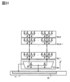
図34は、半導体基板311に設けられた回路を有する素子層411上に、メモリユニット470(メモリユニット470_1乃至メモリユニット470_m:mは2以上の自然数)が積層して設けられた半導体装置の例を示す図である。図34では、素子層411と、素子層411上にメモリユニット470が複数積層されており、複数のメモリユニット470には、それぞれトランジスタ層413(トランジスタ層413_1乃至トランジスタ層413_m)と、各トランジスタ層413上の、複数のメモリデバイス層415(メモリデバイス層415_1乃至メモリデバイス層415_n:nは2以上の自然数)が設けられる例を示している。なお、各メモリユニット470では、トランジスタ層413上にメモリデバイス層415が設けられる例を示しているが、本実施の形態ではこれに限定されない。複数のメモリデバイス層415上にトランジスタ層413を設けてもよいし、トランジスタ層413の上下にメモリデバイス層415が設けられてもよい。
素子層411は、半導体基板311に設けられたトランジスタ300を有し、半導体装置の回路(周辺回路と呼ぶ場合がある)として機能することができる。回路の例としては、カラムドライバ、ロウドライバ、カラムデコーダ、ロウデコーダ、センスアンプ、プリチャージ回路、増幅回路、ワード線ドライバ回路、出力回路、コントロールロジック回路などが挙げられる。
トランジスタ層413は、トランジスタ200Tを有し、各メモリユニット470を制御する回路として機能することができる。メモリデバイス層415は、メモリデバイス420を有する。本実施の形態に示すメモリデバイス420は、トランジスタ200Mと容量素子292を有する。
なお、上記mの値については、特に制限は無いが2以上100以下、好ましくは2以上50以下、さらに好ましくは、2以上10以下である。また、上記nの値については、特に制限は無いが2以上100以下、好ましくは2以上50以下、さらに好ましくは、2以上10以下である。また、上記mとnの積は、4以上256以下、好ましくは4以上128以下、さらに好ましくは4以上64以下である。
また、図34は、メモリユニットに含まれるトランジスタ200T、およびトランジスタ200Mのチャネル長方向の断面図を示す。
図34に示すように、半導体基板311にトランジスタ300が設けられ、トランジスタ300上には、メモリユニット470が有するトランジスタ層413とメモリデバイス層415が設けられ、一つのメモリユニット470内でトランジスタ層413が有するトランジスタ200Tと、メモリデバイス層415が有するメモリデバイス420は、複数の導電体424により電気的に接続され、トランジスタ300と、各メモリユニット470におけるトランジスタ層413が有するトランジスタ200Tは、導電体426により電気的に接続される。また、導電体426は、トランジスタ200Tのソース、ドレイン、ゲートのいずれか一と電気的に接続する導電体428を介して、トランジスタ200Tと電気的に接続することが好ましい。導電体424は、メモリデバイス層415の各層に設けられることが好ましい。また、導電体426は、トランジスタ層413、およびメモリデバイス層415の各層に設けられることが好ましい。
また、詳細は後述するが、導電体424の側面、および導電体426の側面には、水または水素などの不純物や、酸素の透過を抑制する絶縁体を設けることが好ましい。このような絶縁体として、例えば、窒化シリコン、酸化アルミニウム、または窒化酸化シリコンなどを用いればよい。
メモリデバイス420は、トランジスタ200Mと容量素子292を有し、トランジスタ200Mは、トランジスタ層413が有するトランジスタ200Tと同様の構造とすることができる。また、トランジスタ200Tとトランジスタ200Mをまとめてトランジスタ200と称する場合がある。
ここで、トランジスタ200は、チャネルが形成される領域(以下、チャネル形成領域ともいう。)を含む半導体に、酸化物半導体として機能する金属酸化物(以下、酸化物半導体ともいう。)を用いることが好ましい。
酸化物半導体として、例えば、In-M-Zn酸化物(元素Mは、アルミニウム、ガリウム、イットリウム、錫、銅、バナジウム、ベリリウム、ホウ素、チタン、鉄、ニッケル、ゲルマニウム、ジルコニウム、モリブデン、ランタン、セリウム、ネオジム、ハフニウム、タンタル、タングステン、またはマグネシウムなどから選ばれた一種、または複数種)等の金属酸化物を用いるとよい。また、酸化物半導体として、酸化インジウム、In-Ga酸化物、In-Zn酸化物を用いてもよい。なお、インジウムの比率が高い組成の酸化物半導体とすることで、トランジスタのオン電流、または電界効果移動度などを高めることができる。
チャネル形成領域に酸化物半導体を用いたトランジスタ200は、非導通状態において極めてリーク電流が小さいため、低消費電力の半導体装置を提供できる。また、酸化物半導体は、スパッタリング法などを用いて成膜できるため、高集積型の半導体装置を構成するトランジスタ200に用いることができる。
一方、酸化物半導体を用いたトランジスタは、酸化物半導体中の不純物および酸素欠損(VO:oxygen vacancyともいう)によって、その電気特性が変動し、ノーマリーオン特性(ゲート電極に電圧を印加しなくてもチャネルが存在し、トランジスタに電流が流れる特性)となりやすい。
そこで、不純物濃度、および欠陥準位密度が低減された酸化物半導体を用いるとよい。なお、本明細書等において、不純物濃度が低く、欠陥準位密度の低いことを高純度真性または実質的に高純度真性という。
従って、酸化物半導体中の不純物濃度はできる限り低減されていることが好ましい。なお、酸化物半導体中の不純物としては、例えば、水素、窒素、アルカリ金属、アルカリ土類金属、鉄、ニッケル、シリコン等がある。
特に、酸化物半導体に含まれる不純物としての水素は、酸化物半導体中に酸素欠損を形成する場合がある。また、酸素欠損に水素が入った欠陥(以下、VOHと呼ぶ場合がある。)は、キャリアとなる電子を生成する場合がある。さらに、水素の一部が金属原子と結合する酸素と反応し、キャリアとなる電子を生成する場合がある。
従って、水素が多く含まれている酸化物半導体を用いたトランジスタは、ノーマリーオン特性となりやすい。また、酸化物半導体中の水素は、熱、電界などのストレスによって動きやすいため、酸化物半導体に多くの水素が含まれると、トランジスタの信頼性が悪化する恐れもある。
従って、トランジスタ200に用いる酸化物半導体は、水素などの不純物、および酸素欠損が低減された高純度真性な酸化物半導体を用いることが好ましい。
<封止構造>
そこで、外部からの不純物混入を抑制するために、不純物の拡散を抑制する材料(以下、不純物に対するバリア性材料ともいう)を用いて、トランジスタ200を封止するとよい。
なお、本明細書において、バリア性とは、対応する物質の拡散を抑制する機能(透過性が低いともいう)とする。または、対応する物質を、捕獲、および固着する(ゲッタリングともいう)機能とする。
例えば、水素、および酸素に対する拡散を抑制する機能を有する材料として、酸化アルミニウム、酸化ハフニウム、酸化ガリウム、インジウムガリウム亜鉛酸化物、窒化シリコン、または窒化酸化シリコンなどがある。特に、窒化シリコンまたは窒化酸化シリコンは、水素に対するバリア性が高いため、封止する材質として用いることが好ましい。
また、例えば、水素を捕獲、および固着する機能を有する材料として、酸化アルミニウム、酸化ハフニウム、酸化ガリウム、インジウムガリウム亜鉛酸化物、などの金属酸化物がある。
トランジスタ300とトランジスタ200の間には、バリア性を有する層として、絶縁体211、絶縁体212、および絶縁体214が設けられることが好ましい。絶縁体211、絶縁体212、および絶縁体214の少なくとも一つに水素などの不純物の拡散や透過を抑制する材料を用いることで、半導体基板311、トランジスタ300などに含まれる水素や水等の不純物がトランジスタ200に拡散することを抑制できる。また、絶縁体211、絶縁体212、および絶縁体214の少なくとも一つに酸素の透過を抑制する材料を用いることで、トランジスタ200のチャネル、またはトランジスタ層413に含まれる酸素が素子層411に拡散することを抑制できる。例えば、絶縁体211、および絶縁体212として水素や水などの不純物の透過を抑制する材料を用い、絶縁体214として酸素の透過を抑制する材料を用いることが好ましい。また、絶縁体214として水素を吸い取り、吸蔵する特性を有する材料を用いることがさらに好ましい。絶縁体211、および絶縁体212として、例えば、窒化シリコン、窒化酸化シリコンなどの窒化物を用いることができる。絶縁体214として、例えば、酸化アルミニウム、酸化ハフニウム、酸化ガリウム、インジウムガリウム亜鉛酸化物、などの金属酸化物を用いることができる。特に、絶縁体214として、酸化アルミニウムを用いることが好ましい。
また、トランジスタ層413およびメモリデバイス層415の側面、すなわちメモリユニット470の側面には絶縁体287が設けられることが好ましく、メモリユニット470の上面には絶縁体282が設けられることが好ましい。このとき絶縁体282は、絶縁体287と接することが好ましく、絶縁体287は、絶縁体211、絶縁体212、および絶縁体214の少なくとも一つと接することが好ましい。絶縁体287、および絶縁体282として、絶縁体214に用いることができる材料を用いることが好ましい。
また、絶縁体282、および絶縁体287を覆うように絶縁体283、および絶縁体284が設けられることが好ましく、絶縁体283は、絶縁体211、絶縁体212、および絶縁体214の少なくとも一つと接することが好ましい。図34では、絶縁体287が絶縁体214の側面、絶縁体212の側面、および絶縁体211の上面および側面と接し、絶縁体283が絶縁体287の上面および側面、および絶縁体211の上面と接する例を示しているが、本実施の形態はこれに限らない。絶縁体287が絶縁体214の側面、および絶縁体212の上面および側面と接し、絶縁体283が絶縁体287の上面および側面、および絶縁体212の上面と接していてもよい。絶縁体282、および絶縁体287として、絶縁体211、および絶縁体212に用いることができる材料を用いることが好ましい。
上記構造において、絶縁体287、および絶縁体282として酸素の透過を抑制する材料を用いることが好ましい。また、絶縁体287、および絶縁体282として水素を捕獲、および固着する特性を有する材料を用いることがさらに好ましい。トランジスタ200に近接する側に、水素を捕獲、および固着する機能を有する材料を用いることで、トランジスタ200中、またはメモリユニット470中の水素は、絶縁体214、絶縁体287、および絶縁体282に、捕獲、および固着されるため、トランジスタ200中の水素濃度を低減することができる。また、絶縁体283、および絶縁体284として水素や水などの不純物の透過を抑制する材料を用いることが好ましい。
以上のような構造とすることで、メモリユニット470は、絶縁体211、絶縁体212、絶縁体214、絶縁体287、絶縁体282、絶縁体283、および絶縁体284により囲われる。より具体的には、メモリユニット470は、絶縁体214、絶縁体287、および絶縁体282(第1の構造体と表記する場合がある)により囲われ、メモリユニット470、および第1の構造体は、絶縁体211、絶縁体212、絶縁体283、および絶縁体284(第2の構造体と表記する場合がある)により囲われる。また、このようにメモリユニット470を2層以上の複数の構造体により囲う構造を入れ子構造と呼ぶ場合がある。ここで、メモリユニット470が複数の構造体により囲われることを、メモリユニット470が複数の絶縁体により封止されると表記する場合がある。
また、第2の構造体は、第1の構造体を介して、トランジスタ200を封止する。従って、第2の構造体の外方に存在する水素は、第2の構造体により、第2の構造体の内部(トランジスタ200側)への拡散が、抑制される。つまり、第1の構造体は、第2の構造体の内部構造に存在する水素を、効率よく捕獲し、固着することができる。
上記構造として、具体的には、第1の構造体には酸化アルミニウムなどの金属酸化物を用い、第2の構造体には窒化シリコンなどの窒化物を用いることができる。より、具体的には、トランジスタ200と、窒化シリコン膜との間に、酸化アルミニウム膜を配置するとよい。
さらに、構造体に用いる材料は、成膜条件を適宜設定することにより、膜中の水素濃度を低減することができる。
一般的に、CVD法を用いて成膜した膜は、スパッタリング法を用いて成膜した膜よりも、被覆性が高い。一方で、CVD法に用いる化合物ガスは、水素を含む場合が多く、CVD法を用いて成膜した膜は、スパッタリング法を用いて成膜した膜よりも、水素の含有量が多い。
従って、例えば、トランジスタ200と近接する膜に、膜中の水素濃度が低減された膜(具体的にはスパッタリング法を用いて成膜した膜)を用いるとよい。一方で、不純物の拡散を抑制する膜として、被膜性が高い一方で膜中の水素濃度が比較的高い膜(具体的にはCVD法を用いて成膜した膜)を用いる場合、トランジスタ200と、水素濃度が比較的高い一方で被膜性が高い膜との間に、水素を捕獲、および固着する機能を有し、かつ水素濃度が低減された膜を配置するとよい。
つまり、トランジスタ200に近接して配置する膜は、膜中の水素濃度が比較的低い膜を用いるとよい。一方で、膜中の水素濃度が比較的高い膜は、トランジスタ200から遠隔して配置するとよい。
上記構造として、具体的には、トランジスタ200を、CVD法を用いて成膜した窒化シリコンを用いて封止する場合、トランジスタ200と、CVD法を用いて成膜した窒化シリコン膜との間に、スパッタリング法を用いて成膜した酸化アルミニウム膜を配置するとよい。さらに好ましくは、CVD法を用いて成膜した窒化シリコン膜と、スパッタリング法を用いて成膜した酸化アルミニウム膜との間に、スパッタリング法を用いて成膜した窒化シリコン膜を配置するとよい。
なお、CVD法を用いて成膜する場合、水素原子を含まない、または水素原子の含有量が少ない、化合物ガスを用いて成膜することで、成膜した膜に含まれる水素濃度を低減してもよい。
また、各トランジスタ層413とメモリデバイス層415の間、または各メモリデバイス層415の間にも、絶縁体282、および絶縁体214が設けられることが好ましい。また、絶縁体282、および絶縁体214の間に絶縁体296が設けられることが好ましい。絶縁体296は、絶縁体283、および絶縁体284と同様の材料を用いることができる。または、酸化シリコン、酸化窒化シリコンを用いることができる。または、公知の絶縁性材料を用いてもよい。ここで、絶縁体282、絶縁体296、および絶縁体214は、トランジスタ200を構成する要素であってもよい。絶縁体282、絶縁体296、および絶縁体214がトランジスタ200の構成要素を兼ねることで、半導体装置の作製にかかる工程数を削減できるため好ましい。
また、各トランジスタ層413とメモリデバイス層415の間、または各メモリデバイス層415の間に設けられる絶縁体282、絶縁体296、および絶縁体214それぞれの側面は、絶縁体287と接することが好ましい。このような構造とすることで、トランジスタ層413およびメモリデバイス層415は、それぞれ絶縁体282、絶縁体296、絶縁体214、絶縁体287、絶縁体283、および絶縁体284により囲われ、封止される。
また、絶縁体284の周囲には、絶縁体274を設けてもよい。また、絶縁体274、絶縁体284、絶縁体283、および絶縁体211に埋め込むように導電体430を設けてもよい。導電体430は、トランジスタ300、すなわち素子層411に含まれる回路と電気的に接続する。
また、メモリデバイス層415では、容量素子292がトランジスタ200Mと同じ層に形成されているため、メモリデバイス420の高さをトランジスタ200Mと同程度にすることができ、各メモリデバイス層415の高さが過剰に大きくなるのを抑制することができる。これにより、比較的容易に、メモリデバイス層415の数を増やすことができる。例えば、トランジスタ層413、およびメモリデバイス層415からなる積層を100層程度にしてもよい。
<トランジスタ200>
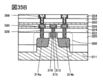
図35(A)を用いて、トランジスタ層413が有するトランジスタ200T、およびメモリデバイス420が有するトランジスタ200Mに用いることができるトランジスタ200について説明する。
図35(A)に示すように、トランジスタ200は、絶縁体216と、導電体205(導電体205a、および導電体205b)と、絶縁体222と、絶縁体224と、酸化物230(酸化物230a、酸化物230b、および酸化物230c)と、導電体242(導電体242a、および導電体242b)と、酸化物243(酸化物243a、および酸化物243b)と、絶縁体272と、絶縁体273と、絶縁体250と、導電体260(導電体260a、および導電体260b)と、を有する。
また、絶縁体216、および導電体205は、絶縁体214上に設けられ、絶縁体273上には絶縁体280、および絶縁体282が設けられる。絶縁体214、絶縁体280、および絶縁体282は、トランジスタ200の一部を構成しているとみなすことができる。
また、本発明の一態様の半導体装置は、トランジスタ200と電気的に接続し、プラグとして機能する導電体240(導電体240a、および導電体240b)を有する。なお、プラグとして機能する導電体240の側面に接して絶縁体241(絶縁体241a、および絶縁体241b)を設けてもよい。また、絶縁体282上、および導電体240上には、導電体240と電気的に接続し、配線として機能する導電体246(導電体246a、および導電体246b)が設けられる。
また、導電体240aおよび導電体240bは、タングステン、銅、またはアルミニウムを主成分とする導電性材料を用いることが好ましい。また、導電体240aおよび導電体240bは積層構造としてもよい。
また、導電体240を積層構造とする場合、水または水素などの不純物、および酸素の透過を抑制する機能を有する導電性材料を用いることが好ましい。例えば、タンタル、窒化タンタル、チタン、窒化チタン、ルテニウム、または酸化ルテニウムなどを用いることが好ましい。また、水または水素などの不純物、および酸素の透過を抑制する機能を有する導電性材料は、単層または積層で用いてもよい。当該導電性材料を用いることで、絶縁体280などから拡散する水または水素などの不純物が、導電体240aおよび導電体240bを通じて酸化物230に混入するのをさらに低減することができる。また、絶縁体280に添加された酸素が導電体240aおよび導電体240bに吸収されるのを防ぐことができる。
また、導電体240の側面に接して設けられる絶縁体241としては、例えば、窒化シリコン、酸化アルミニウム、または窒化酸化シリコンなどを用いればよい。絶縁体241は、絶縁体272、絶縁体273、絶縁体280、および絶縁体282に接して設けられるので、絶縁体280などから水または水素などの不純物が、導電体240aおよび導電体240bを通じて酸化物230に混入するのを抑制することができる。特に、窒化シリコンは水素に対するブロッキング性が高いので好適である。また、絶縁体280に含まれる酸素が導電体240aおよび導電体240bに吸収されるのを防ぐことができる。
導電体246は、タングステン、銅、またはアルミニウムを主成分とする導電性材料を用いることが好ましい。また、当該導電体は、積層構造としてもよく、例えば、チタン又は窒化チタンと上記導電性材料との積層としてもよい。なお、当該導電体は、絶縁体に設けられた開口に埋め込むように形成してもよい。
トランジスタ200において、導電体260は、トランジスタの第1のゲートとして機能し、導電体205は、トランジスタの第2のゲートとして機能する。また、導電体242a、および導電体242bは、ソース電極またはドレイン電極として機能する。
酸化物230は、チャネル形成領域を有する半導体として機能する。
絶縁体250は、第1のゲート絶縁体として機能し、絶縁体222、および絶縁体224は、第2のゲート絶縁体として機能する。
ここで、図35(A)に示すトランジスタ200は、絶縁体280、絶縁体273、絶縁体272、導電体242などに設けた開口部内に、導電体260が、酸化物230cおよび絶縁体250を介して、自己整合的に形成される。
つまり、導電体260は、酸化物230cおよび絶縁体250を介して、絶縁体280などに設けた開口を埋めるように形成されるため、導電体242aと導電体242bの間の領域に、導電体260の位置合わせが不要となる。
ここで、絶縁体280などに設けた開口内に、酸化物230cを設けることが好ましい。従って、絶縁体250、および導電体260は、酸化物230cを介して、酸化物230b、および酸化物230aの積層構造と重畳する領域を有する。当該構造とすることで、酸化物230cと絶縁体250とを連続成膜により形成することが可能となるため、酸化物230と絶縁体250との界面を清浄に保つことができる。従って、界面散乱によるキャリア伝導への影響が小さくなり、トランジスタ200は高いオン電流、および高い周波数特性を得ることができる。
また、図35(A)に示すトランジスタ200は、導電体260の底面、および側面が絶縁体250に接する。また、絶縁体250の底面、および側面は、酸化物230cと接する。
また、トランジスタ200は、図35(A)に示すように、絶縁体282と、酸化物230cとが、直接接する構造となっている。当該構造とすることで、絶縁体280に含まれる酸素の導電体260への拡散を抑制することができる。
従って、絶縁体280に含まれる酸素は、酸化物230cを介して、酸化物230aおよび酸化物230bへ効率よく供給することができるので、酸化物230a中および酸化物230b中の酸素欠損を低減し、トランジスタ200の電気特性および信頼性を向上させることができる。
以下では、本発明の一態様に係るトランジスタ200を有する半導体装置の詳細な構成について説明する。
トランジスタ200は、チャネル形成領域を含む酸化物230(酸化物230a、酸化物230b、および酸化物230c)に、酸化物半導体として機能する金属酸化物(以下、酸化物半導体ともいう)を用いることが好ましい。
例えば、酸化物半導体として機能する金属酸化物は、エネルギーギャップが2eV以上、好ましくは2.5eV以上のものを用いることが好ましい。エネルギーギャップの大きい金属酸化物を用いることで、トランジスタ200の非導通状態におけるリーク電流(オフ電流)を極めて小さくすることができる。このようなトランジスタを用いることで、低消費電力の半導体装置を提供できる。
具体的には、酸化物230として、In-M-Zn酸化物(元素Mは、アルミニウム、ガリウム、イットリウム、錫、銅、バナジウム、ベリリウム、ホウ素、チタン、鉄、ニッケル、ゲルマニウム、ジルコニウム、モリブデン、ランタン、セリウム、ネオジム、ハフニウム、タンタル、タングステン、またはマグネシウムなどから選ばれた一種、または複数種)等の金属酸化物を用いるとよい。特に、元素Mは、アルミニウム、ガリウム、イットリウム、または錫を用いるとよい。また、酸化物230として、In-M酸化物、In-Zn酸化物、またはM-Zn酸化物を用いてもよい。
図35(A)に示すように、酸化物230は、絶縁体224上の酸化物230aと、酸化物230a上の酸化物230bと、酸化物230b上に配置され、少なくとも一部が酸化物230bの上面に接する酸化物230cと、を有することが好ましい。ここで、酸化物230cの側面は、酸化物243a、酸化物243b、導電体242a、導電体242b、絶縁体272、絶縁体273、および絶縁体280に接して設けられていることが好ましい。
つまり、酸化物230は、酸化物230aと、酸化物230a上の酸化物230bと、酸化物230b上の酸化物230cと、を有する。酸化物230b下に酸化物230aを有することで、酸化物230aよりも下方に形成された構造物から、酸化物230bへの不純物の拡散を抑制することができる。また、酸化物230b上に酸化物230cを有することで、酸化物230cよりも上方に形成された構造物から、酸化物230bへの不純物の拡散を抑制することができる。
なお、トランジスタ200では、チャネル形成領域と、その近傍において、酸化物230a、酸化物230b、および酸化物230cの3層を積層する構成について示しているが、本発明はこれに限られるものではない。例えば、酸化物230bの単層、酸化物230bと酸化物230aの2層構造、酸化物230bと酸化物230cの2層構造、または4層以上の積層構造を設ける構成にしてもよい。例えば、酸化物230cを2層構造にして、4層の積層構造を設ける構成にしてもよい。
また、酸化物230は、各金属原子の原子数比が異なる酸化物により、積層構造を有することが好ましい。具体的には、酸化物230aに用いる金属酸化物において、構成元素中の元素Mの原子数比が、酸化物230bに用いる金属酸化物における、構成元素中の元素Mの原子数比より、大きいことが好ましい。また、酸化物230aに用いる金属酸化物において、Inに対する元素Mの原子数比が、酸化物230bに用いる金属酸化物における、Inに対する元素Mの原子数比より大きいことが好ましい。また、酸化物230bに用いる金属酸化物において、元素Mに対するInの原子数比が、酸化物230aに用いる金属酸化物における、元素Mに対するInの原子数比より大きいことが好ましい。また、酸化物230cは、酸化物230aまたは酸化物230bに用いることができる金属酸化物を、用いることができる。
具体的には、酸化物230aとして、In:Ga:Zn=1:3:4[原子数比]もしくはその近傍の組成、または1:1:0.5[原子数比]もしくはその近傍の組成の金属酸化物を用いればよい。
また、酸化物230bとして、In:Ga:Zn=4:2:3[原子数比]もしくはその近傍の組成、または1:1:1[原子数比]もしくはその近傍の組成の金属酸化物を用いればよい。また、酸化物230bとして、In:Ga:Zn=5:1:3[原子数比]もしくはその近傍の組成、またはIn:Ga:Zn=10:1:3[原子数比]もしくはその近傍の組成の金属酸化物を用いてもよい。また、酸化物230bとして、In-Zn酸化物(例えば、In:Zn=2:1[原子数比]もしくはその近傍の組成、In:Zn=5:1[原子数比]もしくはその近傍の組成、またはIn:Zn=10:1[原子数比]もしくはその近傍の組成)を用いてもよい。また、酸化物230bとして、In酸化物を用いてもよい。
また、酸化物230cとして、In:Ga:Zn=1:3:4[原子数比もしくはその近傍の組成]、Ga:Zn=2:1[原子数比]もしくはその近傍の組成、またはGa:Zn=2:5[原子数比]もしくはその近傍の組成の金属酸化物を用いればよい。また、酸化物230cに、酸化物230bに用いることのできる材料を適用し、単層または積層で設けてもよい。例えば、酸化物230cを積層構造とする場合の具体例としては、In:Ga:Zn=4:2:3[原子数比]もしくはその近傍の組成と、In:Ga:Zn=1:3:4[原子数比]もしくはその近傍の組成との積層構造、Ga:Zn=2:1[原子数比]もしくはその近傍の組成と、In:Ga:Zn=4:2:3[原子数比]もしくはその近傍の組成との積層構造、Ga:Zn=2:5[原子数比]もしくはその近傍の組成と、In:Ga:Zn=4:2:3[原子数比]もしくはその近傍の組成との積層構造、酸化ガリウムと、In:Ga:Zn=4:2:3[原子数比]もしくはその近傍の組成との積層構造などが挙げられる。
なお、実施の形態1に示す、メモリセルアレイ30が有するOSトランジスタの構成と、素子層40が有するOSトランジスタの構成と、を異ならせてもよい。例えば、メモリセルアレイ30に設けられるOSトランジスタが有する酸化物230cには、In:Ga:Zn=4:2:3[原子数比]もしくはその近傍の組成の金属酸化物を用い、素子層40に設けられるOSトランジスタが有する酸化物230cには、In:Ga:Zn=5:1:3[原子数比]もしくはその近傍の組成、In:Ga:Zn=10:1:3[原子数比]もしくはその近傍の組成、In:Zn=10:1[原子数比]もしくはその近傍の組成、In:Zn=5:1[原子数比]もしくはその近傍の組成、In:Zn=2:1[原子数比]もしくはその近傍の組成の金属酸化物を用いればよい。
また、酸化物230b、酸化物230cにおいて、膜中のインジウムの比率を高めることで、トランジスタのオン電流、または電界効果移動度などを高めることが出来るため、好適である。また、上述した近傍の組成とは、所望の原子数比の±30%の範囲を含む。
また、酸化物230bは、結晶性を有していてもよい。例えば、後述するCAAC-OS(c-axis aligned crystalline oxide semiconductor)を用いることが好ましい。CAAC-OSなどの結晶性を有する酸化物は、不純物や欠陥(酸素欠損など)が少なく、結晶性の高い、緻密な構造を有している。よって、ソース電極またはドレイン電極による、酸化物230bからの酸素の引き抜きを抑制することができる。また、加熱処理を行っても、酸化物230bから酸素が、引き抜かれることを低減できるので、トランジスタ200は、製造工程における高い温度(所謂サーマルバジェット)に対して安定である。
導電体205は、酸化物230、および導電体260と、重なるように配置する。また、導電体205は、絶縁体216に埋め込まれて設けることが好ましい。
導電体205がゲート電極として機能する場合、導電体205に印加する電位を、導電体260に印加する電位と、連動させず、独立して変化させることで、トランジスタ200のしきい値電圧(Vth)を制御することができる。特に、導電体205に負の電位を印加することにより、トランジスタ200のVthをより大きくし、オフ電流を低減することが可能となる。したがって、導電体205に負の電位を印加したほうが、印加しない場合よりも、導電体260に印加する電位が0Vのときのドレイン電流を小さくすることができる。
なお、導電体205は、図35(A)に示すように、酸化物230の導電体242aおよび導電体242bと重ならない領域の大きさよりも、大きく設けるとよい。ここで図示しないが、導電体205は、酸化物230のチャネル幅方向において酸化物230a、および酸化物230bよりも外側の領域まで延伸していることが好ましい。つまり、酸化物230のチャネル幅方向における側面の外側において、導電体205と、導電体260とは、絶縁体を介して重畳していることが好ましい。導電体205を大きく設けることによって、導電体205形成以降の作製工程のプラズマを用いた処理において、局所的なチャージング(チャージアップと言う)の緩和ができる場合がある。ただし、本発明の一態様はこれに限定されない。導電体205は、少なくとも導電体242aと、導電体242bとの間に位置する酸化物230と重畳すればよい。
また、絶縁体224の底面を基準として、酸化物230aおよび酸化物230bと、導電体260とが、重ならない領域における導電体260の底面の高さは、酸化物230bの底面の高さより低い位置に配置されていることが好ましい。
図示しないが、チャネル幅方向において、ゲートとして機能する導電体260は、チャネル形成領域の酸化物230bの側面および上面を酸化物230cおよび絶縁体250を介して覆う構造とすることにより、導電体260から生じる電界を、酸化物230bに生じるチャネル形成領域全体に作用させやすくなる。従って、トランジスタ200のオン電流を増大させ、周波数特性を向上させることができる。本明細書において、導電体260、および導電体205の電界によって、チャネル形成領域を電気的に取り囲むトランジスタの構造を、surrounded channel(S-channel)構造とよぶ。
また、導電体205aは、水または水素などの不純物および酸素の透過を抑制する導電体が好ましい。例えば、チタン、窒化チタン、タンタル、または窒化タンタルを用いることができる。また、導電体205bは、タングステン、銅、またはアルミニウムを主成分とする導電性材料を用いることが好ましい。なお、導電体205を2層で図示したが、3層以上の多層構造としてもよい。
ここで、酸化物半導体と、酸化物半導体の下層に位置する絶縁体、または導電体と、酸化物半導体の上層に位置する絶縁体、または導電体とを、大気開放を行わずに、異なる膜種を連続成膜することで、不純物(特に、水素、水)の濃度が低減された、実質的に高純度真性である酸化物半導体膜を成膜することができるので好ましい。
絶縁体222、および絶縁体272および絶縁体273の少なくとも一つは、水または水素などの不純物が、基板側から、または、上方からトランジスタ200に混入するのを抑制するバリア絶縁膜として機能することが好ましい。したがって、絶縁体222、絶縁体272、および絶縁体273の少なくとも一つは、水素原子、水素分子、水分子、窒素原子、窒素分子、酸化窒素分子(N2O、NO、NO2など)、銅原子などの不純物の拡散を抑制する機能を有する(上記不純物が透過しにくい)絶縁性材料を用いることが好ましい。または、酸素(例えば、酸素原子、酸素分子などの少なくとも一)の拡散を抑制する機能を有する(上記酸素が透過しにくい)絶縁性材料を用いることが好ましい。
例えば、絶縁体273として、窒化シリコンまたは窒化酸化シリコンなどを用い、絶縁体222および絶縁体272として、酸化アルミニウムまたは酸化ハフニウムなどを用いることが好ましい。
これにより、水または水素などの不純物が絶縁体222を介して、トランジスタ200側に拡散するのを抑制することができる。または、絶縁体224などに含まれる酸素が、絶縁体222を介して基板側に、拡散するのを抑制することができる。
また、水または水素などの不純物が、絶縁体272および絶縁体273を介して配置されている絶縁体280などからトランジスタ200側に拡散するのを抑制することができる。このように、トランジスタ200を、水または水素などの不純物、および酸素の拡散を抑制する機能を有する絶縁体272、および絶縁体273で取り囲む構造とすることが好ましい。
ここで、酸化物230と接する絶縁体224は、加熱により酸素を脱離することが好ましい。本明細書では、加熱により離脱する酸素を過剰酸素と呼ぶことがある。例えば、絶縁体224は、酸化シリコンまたは酸化窒化シリコンなどを適宜用いればよい。酸素を含む絶縁体を酸化物230に接して設けることにより、酸化物230中の酸素欠損を低減し、トランジスタ200の信頼性を向上させることができる。
絶縁体224として、具体的には、加熱により一部の酸素が脱離する酸化物材料を用いることが好ましい。加熱により酸素を脱離する酸化物とは、昇温脱離ガス分析(TDS(Thermal Desorption Spectroscopy)分析)にて、酸素分子の脱離量が1.0×10¹⁸molecules/cm3以上、好ましくは1.0×1019molecules/cm3以上、さらに好ましくは2.0×1019molecules/cm3以上、または3.0×1020molecules/cm3以上である酸化物膜である。なお、上記TDS分析時における膜の表面温度としては100℃以上700℃以下、または100℃以上400℃以下の範囲が好ましい。
絶縁体222は、水または水素などの不純物が、基板側からトランジスタ200に混入するのを抑制するバリア絶縁膜として機能することが好ましい。例えば、絶縁体222は、絶縁体224より水素透過性が低いことが好ましい。絶縁体222、および絶縁体283によって、絶縁体224および酸化物230などを囲むことにより、外方から水または水素などの不純物がトランジスタ200に侵入することを抑制することができる。
さらに、絶縁体222は、酸素(例えば、酸素原子、酸素分子などの少なくとも一)の拡散を抑制する機能を有する(上記酸素が透過しにくい)ことが好ましい。例えば、絶縁体222は、絶縁体224より酸素透過性が低いことが好ましい。絶縁体222が、酸素や不純物の拡散を抑制する機能を有することで、酸化物230が有する酸素が、絶縁体222より下側へ拡散することを低減できるので、好ましい。また、導電体205が、絶縁体224や、酸化物230が有する酸素と反応することを抑制することができる。
絶縁体222は、絶縁性材料であるアルミニウムおよびハフニウムの一方または双方の酸化物を含む絶縁体を用いるとよい。アルミニウムおよびハフニウムの一方または双方の酸化物を含む絶縁体として、酸化アルミニウム、酸化ハフニウム、アルミニウムおよびハフニウムを含む酸化物(ハフニウムアルミネート)などを用いることが好ましい。このような材料を用いて絶縁体222を形成した場合、絶縁体222は、酸化物230からの酸素の放出や、トランジスタ200の周辺部から酸化物230への水素等の不純物の混入を抑制する層として機能する。
または、これらの絶縁体に、例えば、酸化アルミニウム、酸化ビスマス、酸化ゲルマニウム、酸化ニオブ、酸化シリコン、酸化チタン、酸化タングステン、酸化イットリウム、酸化ジルコニウムを添加してもよい。またはこれらの絶縁体を窒化処理してもよい。上記の絶縁体に酸化シリコン、酸化窒化シリコンまたは窒化シリコンを積層して用いてもよい。
また、絶縁体222は、例えば、酸化アルミニウム、酸化ハフニウム、酸化タンタル、酸化ジルコニウム、チタン酸ジルコン酸鉛(PZT)、チタン酸ストロンチウム(SrTiO3)または(Ba,Sr)TiO3(BST)などのいわゆるhigh-k材料を含む絶縁体を単層または積層で用いてもよい。例えば、絶縁体222を積層とする場合、酸化ジルコニウムと、酸化アルミニウムと、酸化ジルコニウムと、が順に形成された3層積層や、酸化ジルコニウムと、酸化アルミニウムと、酸化ジルコニウムと、酸化アルミニウムと、が順に形成された4層積層などを用いれば良い。また、絶縁体222としては、ハフニウムと、ジルコニウムとが含まれる化合物などを用いても良い。半導体装置の微細化、および高集積化が進むと、ゲート絶縁体、および容量素子に用いる誘電体の薄膜化により、トランジスタや容量素子のリーク電流などの問題が生じる場合がある。ゲート絶縁体、および容量素子に用いる誘電体として機能する絶縁体にhigh-k材料を用いることで、物理膜厚を保ちながら、トランジスタ動作時のゲート電位の低減、および容量素子の容量の確保が可能となる。
なお、絶縁体222、および絶縁体224が、2層以上の積層構造を有していてもよい。その場合、同じ材料からなる積層構造に限定されず、異なる材料からなる積層構造でもよい。
また、酸化物230bと、ソース電極またはドレイン電極として機能する導電体242(導電体242aよび導電体242b)と、の間に酸化物243(酸化物243aおよび酸化物243b)を配置してもよい。導電体242と、酸化物230bとが接しない構成となるので、導電体242が、酸化物230bの酸素を吸収することを抑制できる。つまり、導電体242の酸化を防止することで、導電体242の導電率の低下を抑制することができる。従って、酸化物243は、導電体242の酸化を抑制する機能を有することが好ましい。
ソース電極やドレイン電極として機能する導電体242と酸化物230bとの間に酸素の透過を抑制する機能を有する酸化物243を配置することで、導電体242と、酸化物230bとの間の電気抵抗が低減されるので好ましい。このような構成とすることで、トランジスタ200の電気特性およびトランジスタ200の信頼性を向上させることができる。
酸化物243として、アルミニウム、ガリウム、イットリウム、錫、銅、バナジウム、ベリリウム、ホウ素、チタン、鉄、ニッケル、ゲルマニウム、ジルコニウム、モリブデン、ランタン、セリウム、ネオジム、ハフニウム、タンタル、タングステン、またはマグネシウムなどから選ばれた一種、または複数種からなる元素Mを有する金属酸化物を用いてもよい。特に、元素Mは、アルミニウム、ガリウム、イットリウム、または錫を用いるとよい。酸化物243は、酸化物230bよりも元素Mの濃度が高いことが好ましい。また、酸化物243として、酸化ガリウムを用いてもよい。また、酸化物243として、In-M-Zn酸化物等の金属酸化物を用いてもよい。具体的には、酸化物243に用いる金属酸化物において、Inに対する元素Mの原子数比が、酸化物230bに用いる金属酸化物における、Inに対する元素Mの原子数比より大きいことが好ましい。また、酸化物243の膜厚は、0.5nm以上5nm以下が好ましく、より好ましくは、1nm以上3nm以下である。また、酸化物243は、結晶性を有すると好ましい。酸化物243が結晶性を有する場合、酸化物230中の酸素の放出を好適に抑制することが出来る。例えば、酸化物243としては、六方晶などの結晶構造であれば、酸化物230中の酸素の放出を抑制できる場合がある。
なお、酸化物243は必ずしも設けなくてもよい。その場合、導電体242(導電体242a、および導電体242b)と酸化物230とが接することで、酸化物230中の酸素が導電体242へ拡散し、導電体242が酸化する場合がある。導電体242が酸化することで、導電体242の導電率が低下する蓋然性が高い。なお、酸化物230中の酸素が導電体242へ拡散することを、導電体242が酸化物230中の酸素を吸収する、と言い換えることができる。
また、酸化物230中の酸素が導電体242(導電体242a、および導電体242b)へ拡散することで、導電体242aと酸化物230bとの間、および、導電体242bと酸化物230bとの間に異層が形成される場合がある。当該異層は、導電体242よりも酸素を多く含むため、当該異層は絶縁性を有すると推定される。このとき、導電体242と、当該異層と、酸化物230bとの3層構造は、金属-絶縁体-半導体からなる3層構造とみなすことができ、MIS(Metal-Insulator-Semiconductor)構造と呼ぶ、またはMIS構造を主としたダイオード接合構造と呼ぶ場合がある。
なお、上記異層は、導電体242と酸化物230bとの間に形成されることに限られず、例えば、異層が、導電体242と酸化物230cとの間に形成される場合や、導電体242と酸化物230bとの間、および導電体242と酸化物230cとの間に形成される場合がある。
酸化物243上には、ソース電極、およびドレイン電極として機能する導電体242(導電体242a、および導電体242b)が設けられる。導電体242の膜厚は、例えば、1nm以上50nm以下、好ましくは2nm以上25nm以下、とすればよい。
導電体242としては、アルミニウム、クロム、銅、銀、金、白金、タンタル、ニッケル、チタン、モリブデン、タングステン、ハフニウム、バナジウム、ニオブ、マンガン、マグネシウム、ジルコニウム、ベリリウム、インジウム、ルテニウム、イリジウム、ストロンチウム、ランタンから選ばれた金属元素、または上述した金属元素を成分とする合金か、上述した金属元素を組み合わせた合金等を用いることが好ましい。例えば、窒化タンタル、窒化チタン、タングステン、チタンとアルミニウムを含む窒化物、タンタルとアルミニウムを含む窒化物、酸化ルテニウム、窒化ルテニウム、ストロンチウムとルテニウムを含む酸化物、ランタンとニッケルを含む酸化物などを用いることが好ましい。また、窒化タンタル、窒化チタン、チタンとアルミニウムを含む窒化物、タンタルとアルミニウムを含む窒化物、酸化ルテニウム、窒化ルテニウム、ストロンチウムとルテニウムを含む酸化物、ランタンとニッケルを含む酸化物は、酸化しにくい導電性材料、または、酸素を吸収しても導電性を維持する材料であるため、好ましい。
絶縁体272は、導電体242上面に接して設けられており、バリア層として機能することが好ましい。当該構成にすることで、導電体242による、絶縁体280が有する過剰酸素の吸収を抑制することができる。また、導電体242の酸化を抑制することで、トランジスタ200と配線とのコンタクト抵抗の増加を抑制することができる。よって、トランジスタ200に良好な電気特性および信頼性を与えることができる。
従って、絶縁体272は、酸素の拡散を抑制する機能を有することが好ましい。例えば、絶縁体272は、絶縁体280よりも酸素の拡散を抑制する機能を有することが好ましい。絶縁体272としては、例えば、アルミニウムおよびハフニウムの一方または双方の酸化物を含む絶縁体を成膜するとよい。また、絶縁体272としては、例えば、窒化アルミニウムを含む絶縁体を用いればよい。
図35(A)に示すように、絶縁体272は、導電体242bの上面の一部、および導電体242bの側面と接する。また、図示しないが、絶縁体272は、導電体242aの上面の一部、および導電体242aの側面と接する。また、絶縁体272上に絶縁体273が配置されている。このようにすることで、例えば絶縁体280に添加された酸素が、導電体242吸収されることを抑制することができる。
絶縁体250は、ゲート絶縁体として機能する。絶縁体250は、酸化物230cの上面に接して配置することが好ましい。絶縁体250は、酸化シリコン、酸化窒化シリコン、窒化酸化シリコン、窒化シリコン、フッ素を添加した酸化シリコン、炭素を添加した酸化シリコン、炭素および窒素を添加した酸化シリコン、空孔を有する酸化シリコンを用いることができる。特に、酸化シリコン、および酸化窒化シリコンは熱に対し安定であるため好ましい。
絶縁体224と同様に、絶縁体250は、加熱により酸素が放出される絶縁体を用いて形成することが好ましい。加熱により酸素が放出される絶縁体を、絶縁体250として、酸化物230cの上面に接して設けることにより、酸化物230bのチャネル形成領域に効果的に酸素を供給することができる。また、絶縁体224と同様に、絶縁体250中の水または水素などの不純物濃度が低減されていることが好ましい。絶縁体250の膜厚は、1nm以上20nm以下とするのが好ましい。
また、絶縁体250と導電体260との間に金属酸化物を設けてもよい。当該金属酸化物は、絶縁体250から導電体260への酸素拡散を抑制することが好ましい。酸素の拡散を抑制する金属酸化物を設けることで、絶縁体250から導電体260への酸素の拡散が抑制される。つまり、酸化物230へ供給する酸素量の減少を抑制することができる。また、絶縁体250の酸素による導電体260の酸化を抑制することができる。
また、当該金属酸化物は、ゲート絶縁体の一部としての機能を有する場合がある。したがって、絶縁体250に酸化シリコンや酸化窒化シリコンなどを用いる場合、当該金属酸化物は、比誘電率が高いhigh-k材料である金属酸化物を用いることが好ましい。ゲート絶縁体を、絶縁体250と当該金属酸化物との積層構造とすることで、熱に対して安定、かつ比誘電率の高い積層構造とすることができる。したがって、ゲート絶縁体の物理膜厚を保持したまま、トランジスタ動作時に印加するゲート電位の低減化が可能となる。また、ゲート絶縁体として機能する絶縁体の等価酸化膜厚(EOT)の薄膜化が可能となる。
具体的には、ハフニウム、アルミニウム、ガリウム、イットリウム、ジルコニウム、タングステン、チタン、タンタル、ニッケル、ゲルマニウム、または、マグネシウムなどから選ばれた一種、または二種以上が含まれた金属酸化物を用いることができる。特に、アルミニウム、またはハフニウムの一方または双方の酸化物を含む絶縁体である、酸化アルミニウム、酸化ハフニウム、アルミニウムおよびハフニウムを含む酸化物(ハフニウムアルミネート)などを用いることが好ましい。
または、当該金属酸化物は、ゲートの一部としての機能を有する場合がある。この場合は、酸素を含む導電性材料をチャネル形成領域側に設けるとよい。酸素を含む導電性材料をチャネル形成領域側に設けることで、当該導電性材料から離脱した酸素がチャネル形成領域に供給されやすくなる。
特に、ゲートとして機能する導電体として、チャネルが形成される金属酸化物に含まれる金属元素および酸素を含む導電性材料を用いることが好ましい。また、前述した金属元素および窒素を含む導電性材料を用いてもよい。また、インジウム錫酸化物、酸化タングステンを含むインジウム酸化物、酸化タングステンを含むインジウム亜鉛酸化物、酸化チタンを含むインジウム酸化物、酸化チタンを含むインジウム錫酸化物、インジウム亜鉛酸化物、シリコンを添加したインジウム錫酸化物を用いてもよい。また、窒素を含むインジウムガリウム亜鉛酸化物を用いてもよい。このような材料を用いることで、チャネルが形成される金属酸化物に含まれる水素を捕獲することができる場合がある。または、外方の絶縁体などから混入する水素を捕獲することができる場合がある。
導電体260は、図35(A)では2層構造として示しているが、単層構造でもよいし、3層以上の積層構造であってもよい。
導電体260aは、水素原子、水素分子、水分子、窒素原子、窒素分子、酸化窒素分子(N2O、NO、NO2など)、銅原子などの不純物の拡散を抑制する機能を有する導電性材料を用いることが好ましい。または、酸素(例えば、酸素原子、酸素分子などの少なくとも一)の拡散を抑制する機能を有する導電性材料を用いることが好ましい。
また、導電体260aが酸素の拡散を抑制する機能を持つことにより、絶縁体250に含まれる酸素により、導電体260bが酸化して導電率が低下することを抑制することができる。酸素の拡散を抑制する機能を有する導電性材料としては、例えば、タンタル、窒化タンタル、ルテニウム、または酸化ルテニウムなどを用いることが好ましい。
また、導電体260bは、タングステン、銅、またはアルミニウムを主成分とする導電性材料を用いることが好ましい。また、導電体260は、配線としても機能するため、導電性が高い導電体を用いることが好ましい。例えば、タングステン、銅、またはアルミニウムを主成分とする導電性材料を用いることができる。また、導電体260bは積層構造としてもよく、例えば、チタン又は窒化チタンと上記導電性材料との積層構造としてもよい。
<<金属酸化物>>
酸化物230として、酸化物半導体として機能する金属酸化物を用いることが好ましい。以下では、本発明に係る酸化物230に適用可能な金属酸化物について説明する。
金属酸化物は、少なくともインジウムまたは亜鉛を含むことが好ましい。特に、インジウムおよび亜鉛を含むことが好ましい。また、それらに加えて、ガリウム、イットリウム、錫などが含まれていることが好ましい。また、ホウ素、チタン、鉄、ニッケル、ゲルマニウム、ジルコニウム、モリブデン、ランタン、セリウム、ネオジム、ハフニウム、タンタル、タングステン、マグネシウムなどから選ばれた一種、または複数種が含まれていてもよい。
ここでは、金属酸化物が、インジウム、元素Mおよび亜鉛を有するIn-M-Zn酸化物(元素Mは、アルミニウム、ガリウム、イットリウム、錫、銅、バナジウム、ベリリウム、ホウ素、チタン、鉄、ニッケル、ゲルマニウム、ジルコニウム、モリブデン、ランタン、セリウム、ネオジム、ハフニウム、タンタル、タングステン、またはマグネシウムなどから選ばれた一種、または複数種)である場合を考える。特に、元素Mは、アルミニウム、ガリウム、イットリウム、または錫を用いるとよい。
なお、本明細書等において、窒素を有する金属酸化物も金属酸化物(metal oxide)と総称する場合がある。また、窒素を有する金属酸化物を、金属酸窒化物(metal oxynitride)と呼称してもよい。
<トランジスタ300>
図35(B)を用いてトランジスタ300を説明する。トランジスタ300は、半導体基板311上に設けられ、ゲートとして機能する導電体316、ゲート絶縁体として機能する絶縁体315、半導体基板311の一部からなる半導体領域313、およびソース領域またはドレイン領域として機能する低抵抗領域314a、および低抵抗領域314bを有する。トランジスタ300は、pチャネル型、あるいはnチャネル型のいずれでもよい。
ここで、図35(B)に示すトランジスタ300はチャネルが形成される半導体領域313(半導体基板311の一部)が凸形状を有する。また、半導体領域313の側面および上面を、絶縁体315を介して、導電体316が覆うように設けられている。なお、導電体316は仕事関数を調整する材料を用いてもよい。このようなトランジスタ300は半導体基板311の凸部を利用していることからFIN型トランジスタとも呼ばれる。なお、凸部の上部に接して、凸部を形成するためのマスクとして機能する絶縁体を有していてもよい。また、ここでは半導体基板311の一部を加工して凸部を形成する場合を示したが、SOI基板を加工して凸形状を有する半導体膜を形成してもよい。
なお、図35(B)に示すトランジスタ300は一例であり、その構造に限定されず、回路構成や駆動方法に応じて適切なトランジスタを用いればよい。
<メモリデバイス420>
次に、図36(A)を用いて、図34に示すメモリデバイス420について説明する。なお、メモリデバイス420が有するトランジスタ200Mについて、トランジスタ200と重複する説明は省略する。
メモリデバイス420において、トランジスタ200Mの導電体242aは、容量素子292の電極の一方として機能し、絶縁体272、および絶縁体273は、誘電体として機能する。絶縁体272、および絶縁体273を間に挟み、導電体242aと重畳するように導電体290が設けられ、容量素子292の電極の他方として機能する。導電体290は、隣接するメモリデバイス420が有する容量素子292の電極の他方として用いてもよい。または、導電体290は、隣接するメモリデバイス420が有する導電体290と電気的に接続してもよい。
導電体290は、絶縁体272および絶縁体273を間に挟み、導電体242aの上面および導電体242aの側面にも配置される。このとき容量素子292は、導電体242aと導電体290が重畳する面積により得られる容量より大きい容量が得られるため、好ましい。
導電体424は、導電体242bと電気的に接続し、かつ導電体205を介して下層に位置する導電体424と電気的に接続する。
容量素子292の誘電体として、窒化シリコン、窒化酸化シリコン、酸化アルミニウム、および酸化ハフニウムなどを用いることができる。また、これらの材料を積層して用いることができる。容量素子292の誘電体を積層構造とする場合、酸化アルミニウムと窒化シリコンの積層、酸化ハフニウムと酸化シリコンの積層を用いることができる。ここで、積層の上下は限定されない。例えば、酸化アルミニウムの上に窒化シリコンが積層されてもよいし、窒化シリコンの上に酸化アルミニウムが積層されてもよい。
また、容量素子292の誘電体として、上記材料よりも高い誘電率を有する酸化ジルコニウムを用いてもよい。容量素子292の誘電体として、酸化ジルコニウムを単層で用いてもよいし、積層の一部として用いてもよい。例えば、酸化ジルコニウムと酸化アルミニウムの積層を用いることができる。また、容量素子292の誘電体を3層の積層としてもよく、第1の層、および第3の層に酸化ジルコニウムを用い、第1の層および第3の層の間の第2の層に酸化アルミニウムを用いてもよい。
容量素子292の誘電体として高い誘電率を有する酸化ジルコニウムを用いることで、容量素子292がメモリデバイス420に占める面積を削減できる。そのため、メモリデバイス420に必要な面積を削減でき、ビットコストを向上させることができ好ましい。
また、導電体290として、導電体205、導電体242、導電体260、導電体424などに用いることができる材料を用いることができる。
本実施の形態では、導電体424を間に挟み、トランジスタ200Mおよび容量素子292が対称に配置される例を示している。このように一対のトランジスタ200Mおよび容量素子292を配置することにより、トランジスタ200Mと電気的に接続する導電体424の数を減らすことができる。そのため、メモリデバイス420に必要な面積を削減でき、ビットコストを向上させることができ好ましい。
導電体424の側面に絶縁体241が設けられている場合、導電体424は、導電体242bの上面の少なくとも一部と接続する。
導電体424および導電体205を用いることで、メモリユニット470内のトランジスタ200Tとメモリデバイス420を電気的に接続することができる。
<メモリデバイス420の変形例1>
次に、図36(B)を用いて、メモリデバイス420の変形例として、メモリデバイス420Aを説明する。メモリデバイス420Aは、トランジスタ200Mと、トランジスタ200Mと電気的に接続する容量素子292Aを有する。容量素子292Aは、トランジスタ200Mの下方に設けられる。
メモリデバイス420Aでは、導電体242aは、酸化物243a、酸化物230b、酸化物230a、絶縁体224、および絶縁体222に設けられた開口内に配置され、該開口底部で導電体205と電気的に接続する。導電体205は、容量素子292Aと電気的に接続する。
容量素子292Aは、電極の一方として機能する導電体294と、誘電体として機能する絶縁体295と、電極の他方として機能する導電体297を有する。導電体297は、絶縁体295を間に挟み、導電体294と重畳する。また、導電体297は、導電体205と電気的に接続する。
導電体294は、絶縁体296上に設けられた絶縁体298に形成された開口の底部および側面に設けられ、絶縁体295は、絶縁体298、および導電体294を覆うように設けられる。また、導電体297は、絶縁体295が有する凹部に埋め込まれるように設けられる。
また、絶縁体296に埋め込まれるように導電体299が設けられており、導電体299は、導電体294と電気的に接続する。導電体299は、隣接するメモリデバイス420Aの導電体294と電気的に接続してもよい。
導電体297は、絶縁体295を間に挟み、導電体294の上面および導電体294の側面にも配置される。このとき容量素子292Aは、導電体294と導電体297が重畳する面積により得られる容量より大きい容量が得られるため、好ましい。
容量素子292Aの誘電体として機能する絶縁体295として、窒化シリコン、窒化酸化シリコン、酸化アルミニウム、および酸化ハフニウムなどを用いることができる。また、これらの材料を積層して用いることができる。絶縁体295を積層構造とする場合、酸化アルミニウムと窒化シリコンの積層、酸化ハフニウムと酸化シリコンの積層を用いることができる。ここで、積層の上下は限定されない。例えば、酸化アルミニウムの上に窒化シリコンが積層されてもよいし、窒化シリコンの上に酸化アルミニウムが積層されてもよい。
また、絶縁体295として、上記材料よりも高い誘電率を有する酸化ジルコニウムを用いてもよい。絶縁体295として、酸化ジルコニウムを単層で用いてもよいし、積層の一部として用いてもよい。例えば、酸化ジルコニウムと酸化アルミニウムの積層を用いることができる。また、絶縁体295を3層の積層としてもよく、第1の層、および第3の層に酸化ジルコニウムを用い、第1の層および第3の層の間の第2の層に酸化アルミニウムを用いてもよい。
絶縁体295として高い誘電率を有する酸化ジルコニウムを用いることで、容量素子292Aがメモリデバイス420Aに占める面積を削減できる。そのため、メモリデバイス420Aに必要な面積を削減でき、ビットコストを向上させることができ好ましい。
また、導電体297、導電体294、および導電体299として、導電体205、導電体242、導電体260、導電体424などに用いることができる材料を用いることができる。
また、絶縁体298として、絶縁体214、絶縁体216、絶縁体224、および絶縁体280などに用いることができる材料を用いることができる。
<メモリデバイス420の変形例2>
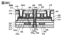
次に、図36(C)を用いて、メモリデバイス420の変形例として、メモリデバイス420Bを説明する。メモリデバイス420Bは、トランジスタ200Mと、トランジスタ200Mと電気的に接続する容量素子292Bを有する。容量素子292Bは、トランジスタ200Mの上方に設けられる。
容量素子292Bは、電極の一方として機能する導電体276と、誘電体として機能する絶縁体277と、電極の他方として機能する導電体278を有する。導電体278は、絶縁体277を間に挟み、導電体276と重畳する。
絶縁体282上に絶縁体275が設けられ、導電体276は、絶縁体275、絶縁体282、絶縁体280、絶縁体273、および絶縁体272に形成された開口の底部および側面に設けられる。絶縁体277は、絶縁体282および導電体276を覆うように設けられる。また、導電体278は、絶縁体277が有する凹部内で導電体276と重畳するように設けられ、少なくともその一部は、絶縁体277を介して絶縁体275上に設けられる。導電体278は、隣接するメモリデバイス420Bが有する容量素子292Bの電極の他方として用いてもよい。または、導電体278は、隣接するメモリデバイス420Bが有する導電体278と電気的に接続してもよい。
導電体278は、絶縁体277を間に挟み、導電体276の上面および導電体276の側面にも配置される。このとき容量素子292Bは、導電体276と導電体278が重畳する面積により得られる容量より大きい容量が得られるため、好ましい。
また、導電体278が有する凹部を埋め込むように絶縁体279を設けてもよい。
容量素子292Bの誘電体として機能する絶縁体277として、窒化シリコン、窒化酸化シリコン、酸化アルミニウム、および酸化ハフニウムなどを用いることができる。また、これらの材料を積層して用いることができる。絶縁体277を積層構造とする場合、酸化アルミニウムと窒化シリコンの積層、酸化ハフニウムと酸化シリコンの積層を用いることができる。ここで、積層の上下は限定されない。例えば、酸化アルミニウムの上に窒化シリコンが積層されてもよいし、窒化シリコンの上に酸化アルミニウムが積層されてもよい。
また、絶縁体277として、上記材料よりも高い誘電率を有する酸化ジルコニウムを用いてもよい。絶縁体277として、酸化ジルコニウムを単層で用いてもよいし、積層の一部として用いてもよい。例えば、酸化ジルコニウムと酸化アルミニウムの積層を用いることができる。また、絶縁体277を3層の積層としてもよく、第1の層、および第3の層に酸化ジルコニウムを用い、第1の層および第3の層の間の第2の層に酸化アルミニウムを用いてもよい。
絶縁体277として高い誘電率を有する酸化ジルコニウムを用いることで、容量素子292Bがメモリデバイス420Bに占める面積を削減できる。そのため、メモリデバイス420Bに必要な面積を削減でき、ビットコストを向上させることができ好ましい。
また、導電体276、および導電体278として、導電体205、導電体242、導電体260、導電体424などに用いることができる材料を用いることができる。
また、絶縁体275、および絶縁体279として、絶縁体214、絶縁体216、絶縁体224、および絶縁体280などに用いることができる材料を用いることができる。
<メモリデバイス420とトランジスタ200Tとの接続>
図34において一点鎖線で囲んだ領域422にて、メモリデバイス420は、導電体424および導電体205を介してトランジスタ200Tのゲートと電気的に接続されているが、本実施の形態はこれに限らない。
図37は、メモリデバイス420が、導電体424、導電体205、導電体246b、および導電体240bを介してトランジスタ200Tのソースおよびドレインの一方として機能する導電体242bと電気的に接続する例を示している。
このように、トランジスタ層413が有する回路の機能に応じてメモリデバイス420とトランジスタ200Tの接続方法を決定することができる。
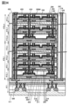
図38は、メモリユニット470がトランジスタ200Tを有するトランジスタ層413と、4層のメモリデバイス層415(メモリデバイス層415_1乃至メモリデバイス層415_4)を有する例を示す。
メモリデバイス層415_1乃至メモリデバイス層415_4は、それぞれ複数のメモリデバイス420を有する。
メモリデバイス420は、導電体424、および導電体205を介して異なるメモリデバイス層415が有するメモリデバイス420、およびトランジスタ層413が有するトランジスタ200Tと電気的に接続する。
メモリユニット470は、絶縁体211、絶縁体212、絶縁体214、絶縁体287、絶縁体282、絶縁体283、および絶縁体284により封止される。絶縁体284の周囲には絶縁体274が設けられる。また、絶縁体274、絶縁体284、絶縁体283、および絶縁体211には導電体430が設けられ、素子層411と電気的に接続する。
また、封止構造の内部には、絶縁体280が設けられる。絶縁体280は、加熱により酸素を放出する機能を有する。または、絶縁体280は、過剰酸素領域を有する。
なお、絶縁体211、絶縁体283、および絶縁体284は、水素に対するブロッキング性が高い機能を有する材料であると好適である。また、絶縁体214、絶縁体282、および絶縁体287は、水素を捕獲、または水素を固着する機能を有する材料であると好適である。
例えば、上記水素に対するブロッキング性が高い機能を有する材料は、窒化シリコン、または窒化酸化シリコンなどが挙げられる。また、上記水素を捕獲、または水素を固着する機能を有する材料は、酸化アルミニウム、酸化ハフニウム、並びにアルミニウムおよびハフニウムを含む酸化物(ハフニウムアルミネート)などが挙げられる。
なお、本明細書において、バリア性とは、対応する物質の拡散を抑制する機能(透過性が低いともいう)とする。または、対応する物質を、捕獲、および固着する(ゲッタリングともいう)機能とする。
なお、絶縁体211、絶縁体212、絶縁体214、絶縁体287、絶縁体282、絶縁体283、および絶縁体284に用いる材料の結晶構造については、特に限定は無いが、非晶質または結晶性を有する構造とすればよい。例えば、水素を捕獲、または水素を固着する機能を有する材料として、非晶質の酸化アルミニウム膜を用いると好適である。非晶質の酸化アルミニウムは、結晶性の高い酸化アルミニウムよりも、水素の捕獲、および固着する量が大きい場合がある。
ここで、絶縁体280中の過剰酸素は、絶縁体280と接する酸化物半導体中の水素の拡散に対し、下記のようなモデルが考えられる。
酸化物半導体中に存在する水素は、酸化物半導体に接する絶縁体280を介して、他の構造体へと拡散する。絶縁体280中の過剰酸素が酸化物半導体中の酸素と反応しOH結合となり、当該水素は絶縁体280中を拡散する。OH結合を有した水素原子は、水素を捕獲、または水素を固着する機能を有する材料(代表的には、絶縁体282)に到達した際に、水素原子は絶縁体282中の原子(例えば、金属原子など)と結合した酸素原子と反応し、絶縁体282中に捕獲、または固着する。一方、OH結合を有していた過剰酸素の酸素原子は、過剰酸素として絶縁体280中に残ると推測される。つまり、当該水素の拡散において、絶縁体280中の過剰酸素が、橋渡し的な役割を担う蓋然性が高い。
上記のモデルを満たすためには、半導体装置の作製プロセスが重要な要素の一つとなる。
一例として、酸化物半導体に、過剰酸素を有する絶縁体280を形成し、その後、絶縁体282を形成する。そのあとに、加熱処理を行うことが好ましい。当該加熱処理は、具体的には、酸素を含む雰囲気、窒素を含む雰囲気、または酸素と窒素の混合雰囲雰囲気にて、350℃以上、好ましくは400℃以上の温度で行う。加熱処理の時間は、1時間以上、好ましくは4時間以上、さらに好ましくは8時間以上とする。
上記の加熱処理によって、酸化物半導体中の水素が、絶縁体280、絶縁体282、および絶縁体287を介して、外方に拡散することができる。つまり、酸化物半導体、および当該酸化物半導体近傍に存在する水素の絶対量を低減することができる。
上記加熱処理のあと、絶縁体283、および絶縁体284を形成する。絶縁体283、および絶縁体284は、水素に対するブロッキング性が高い機能を有する材料であるため、外方に拡散させた水素、または外部に存在する水素を、内部、具体的には、酸化物半導体、または絶縁体280側に入り込むのを抑制することができる。
なお、上記の加熱処理については、絶縁体282を形成したあとに行う構成について、例示したが、これに限定されない。例えば、トランジスタ層413の形成後、またはメモリデバイス層415_1乃至メモリデバイス層415_3の形成後に、それぞれ上記加熱処理を行ってもよい。また、上記加熱処理によって、水素を外方に拡散させる際には、トランジスタ層413の上方または横方向に水素が拡散される。同様に、メモリデバイス層415_1乃至メモリデバイス層415_3形成後に加熱処理をする場合においては、水素は上方または横方向に拡散される。
なお、上記の作製プロセスにおいて、絶縁体211と、絶縁体283と、が接着することで、上述した封止構造が形成される。
以上のように、上記の構造、および上記の作製プロセスとすることで、水素濃度が低減された酸化物半導体を用いた半導体装置を提供することができる。従って、信頼性が良好な半導体装置を提供することができる。また、本発明の一態様により、良好な電気特性を有する半導体装置を提供することができる。
図39(A)乃至図39(C)は、導電体424の配置が図38と異なる例を示す図である。図39(A)は、メモリデバイス420を上面から見たときのレイアウト図を示し、図39(B)は、図39(A)にA1-A2の一点鎖線で示す部位の断面図であり、図39(C)は、図39(A)にB1-B2の一点鎖線で示す部位の断面図である。なお、図39(A)では、図の理解を容易にするため、導電体205の図示を省略する。導電体205を設ける場合、導電体205は、導電体260、および導電体424と重畳する領域を有する。
図39(A)に示すように、導電体424が設けられる開口、すなわち導電体424は、酸化物230a、および酸化物230bと重畳する領域だけでなく、酸化物230a、および酸化物230bの外側にも設けられている。図39(A)では、導電体424が酸化物230a、および酸化物230bのB2側にはみ出すように設けられる例を示しているが、本実施の形態はこれに限定されない。導電体424は酸化物230a、および酸化物230bのB1側にはみ出すように設けられてもよいし、B1側およびB2側の両方ににはみ出すように設けられてもよい。
図39(B)、および図39(C)は、メモリデバイス層415_p-1の上にメモリデバイス層415_pが積層される例を示す(pは、2以上n以下の自然数)。メモリデバイス層415_p-1が有するメモリデバイス420は、導電体424、および導電体205を介して、メモリデバイス層415_pが有するメモリデバイス420と電気的に接続する。
図39(B)では、メモリデバイス層415_p-1において、導電体424は、メモリデバイス層415_p-1の導電体242、およびメモリデバイス層415_pの導電体205と接続する例を示している。ここで、導電体424は、導電体242、酸化物243、酸化物230b、および酸化物230aのB2側の外側でメモリデバイス層415_p-1の導電体205とも接続している。
図39(C)では、導電体424が導電体242、酸化物243、酸化物230b、および酸化物230aのB2側の側面に沿って形成され、絶縁体280、絶縁体273、絶縁体272、絶縁体224、および絶縁体222に形成された開口を介して導電体205と電気的に接続されていることがわかる。ここで、導電体424が導電体242、酸化物243、酸化物230b、および酸化物230aのB2側の側面に沿って設けられる例を図39(B)では点線で示している。また、導電体242、酸化物243、酸化物230b、酸化物230a、絶縁体224、および絶縁体222のB2側の側面と導電体424の間には、絶縁体241が形成される場合がある。
導電体424を導電体242などと重ならない領域にも設けることで、メモリデバイス420は、異なるメモリデバイス層415に設けられたメモリデバイス420と電気的に接続することができる。また、メモリデバイス420は、トランジスタ層413に設けられたトランジスタ200Tとも電気的に接続することができる。
また、導電体424をビット線としたとき、導電体424を導電体242などと重ならない領域にも設けることで、B1-B2方向で隣り合うメモリデバイス420のビット線の距離を拡げることができる。図39(A)に示すように、導電体242上における導電体424同士の間隔は、d1であるが、酸化物230aより下層、すなわち絶縁体224、および絶縁体222に形成された開口内に位置する導電体424同士の間隔はd2となり、d2はd1よりも大きくなる。B1-B2方向で隣り合う導電体424同士の間隔がd1である場合に比べ、一部の間隔をd2とすることで、導電体424の寄生容量を低減することができる。導電体424の寄生容量を低減することで、容量素子292に必要な容量を低減できるため好ましい。
メモリデバイス420では、2つのメモリセルに対して共通のビット線として機能する導電体424を設けている。容量に用いられる誘電体の誘電率や、ビット線間の寄生容量を適宜調整することで、各メモリセルのセルサイズを縮小できる。ここでは、チャネル長を30nm(30nmノードともいう)としたときのメモリセルのセルサイズの見積もり、ビット密度の見積もり、およびビットコストの見積もりについて説明する。なお、以下で説明する図40(A)乃至図40(D)では、図の理解を容易にするため、導電体205の図示を省略する。導電体205を設ける場合、導電体205は、導電体260、および導電体424と重畳する領域を有する。
図40(A)は、容量素子の誘電体として、10nmの厚さの酸化ハフニウムとその上に1nmの酸化シリコンを順に積層し、メモリデバイス420が有する各メモリセルの導電体242、酸化物243、酸化物230a、および酸化物230bの間にはスリットが設けられ、導電体242および該スリットと重畳するようにビット線として機能する導電体424が設けられる例を示す。このようにして得られたメモリセル432をセルAと呼ぶ。
セルAにおけるセルサイズは、45.25F2である。
図40(B)は、容量素子の誘電体として、第1の酸化ジルコニウムと、その上に酸化アルミニウムと、その上に第2の酸化ジルコニウムを順に積層し、メモリデバイス420が有する各メモリセルの導電体242、酸化物243、酸化物230a、および酸化物230bの間にはスリットが設けられ、導電体242および該スリットと重畳するようにビット線として機能する導電体424が設けられる例を示す。このようにして得られたメモリセル433をセルBと呼ぶ。
セルBは、セルAと比較して容量に用いる誘電体の誘電率が高いため、容量素子の面積を縮小できる。よって、セルBでは、セルAと比較して、セルサイズを縮小できる。セルBにおけるセルサイズは、25.53F2である。
セルA、およびセルBは、図34、図36(A)乃至図36(C)、および図37に示すメモリデバイス420、メモリデバイス420A、またはメモリデバイス420Bが有するメモリセルに対応する。
図40(C)は、容量素子の誘電体として、第1の酸化ジルコニウムと、その上に酸化アルミニウムと、その上に第2の酸化ジルコニウムを積層し、メモリデバイス420が有する導電体242、酸化物243、酸化物230a、および酸化物230bを各メモリセルが共有し、導電体242と重畳する一部、および導電体242の外側の一部と重畳するようにビット線として機能する導電体424が設けられる例を示す。このようにして得られたメモリセル434をセルCと呼ぶ。
セルCにおける導電体424の間隔は、導電体242の上方と比較して、酸化物230aより下層において広くなる。そのため、導電体424の寄生容量を低減することができ、容量素子の面積を縮小できる。また、導電体242、酸化物243、酸化物230a、および酸化物230bにスリットを設けない。以上より、セルCでは、セルAおよびセルBと比較して、セルサイズを縮小できる。セルCにおけるセルサイズは、17.20F2である。
図40(D)は、セルCにおいて導電体205および絶縁体216を設けない例を示す。このようなメモリセル435をセルDと呼ぶ。
セルDにおいて導電体205および絶縁体216を設けないことで、メモリデバイス420を薄くすることができる。そのため、メモリデバイス420を有するメモリデバイス層415を薄くすることができ、メモリデバイス層415を複数積層したメモリユニット470の高さを低くすることができる。導電体424および導電体205をビット線とみなしたとき、メモリユニット470内でビット線を短くすることができる。ビット線を短くできるため、ビット線の寄生負荷が低減され、導電体424の寄生容量をさらに低減することができ、容量素子の面積を縮小できる。また、導電体242、酸化物243、酸化物230a、および酸化物230bにスリットを設けない。以上より、セルDでは、セルA、セルB、およびセルCと比較して、セルサイズを縮小できる。セルDにおけるセルサイズは、15.12F2である。
セルC、およびセルDは、図39(A)乃至図39(C)に示すメモリデバイス420が有するメモリセルに対応する。
ここで、セルA乃至セルD、およびセルDにおいて多値化を行ったセルEについてビット密度、およびビットコストCbの見積もりを行った。また、得られた見積もりについて現在市販されているDRAMにおけるビット密度、およびビットコストの予想値と比較した。
本発明の一態様の半導体装置におけるビットコストCbは、数式1を用いて見積もった。
ここで、nはメモリデバイス層の積層数、Pcは共通部分として主に素子層411のパターニング回数、Psはメモリデバイス層415およびトランジスタ層413の1層あたりのパターニング回数、DdはDRAMのビット密度、D3dはメモリデバイス層415の1層のビット密度、PdはDRAMのパターニング回数を示す。ただし、Pdにおいて、スケーリングに伴う増加分を含む。
表1に、市販されているDRAMのビット密度の予想値、および本発明の一態様の半導体装置のビット密度の見積もりを示す。なお、市販されているDRAMは、プロセスノードが18nm、および1Xnmの2種類である。また、本発明の一態様の半導体装置のプロセスノードは30nmとし、セルA乃至セルEにおけるメモリデバイス層の積層数を5層、10層、および20層としてビット密度の見積もりを行った。
表2に、市販されているDRAMのビットコストから、本発明の一態様の半導体装置の相対ビットコストを見積もった結果を示す。なお、ビットコストの比較には、プロセスノードが1XnmのDRAMを用いた。また、本発明の一態様の半導体装置のプロセスノードは30nmとし、セルA乃至セルDにおけるメモリデバイス層の積層数を5層、10層、および20層として見積もりを行った。
本実施の形態に示す構成は、他の実施の形態などに示す構成と適宜組み合わせて用いることができる。
(実施の形態10)
本実施の形態では、上記の実施の形態で説明したOSトランジスタに用いることができる金属酸化物(以下、酸化物半導体ともいう。)について説明する。
金属酸化物は、少なくともインジウムまたは亜鉛を含むことが好ましい。特にインジウムおよび亜鉛を含むことが好ましい。また、それらに加えて、アルミニウム、ガリウム、イットリウム、スズなどが含まれていることが好ましい。また、ホウ素、チタン、鉄、ニッケル、ゲルマニウム、ジルコニウム、モリブデン、ランタン、セリウム、ネオジム、ハフニウム、タンタル、タングステン、マグネシウム、コバルトなどから選ばれた一種、または複数種が含まれていてもよい。
<結晶構造の分類>
まず、酸化物半導体における、結晶構造の分類について、図41(A)を用いて説明を行う。図41(A)は、酸化物半導体、代表的にはIGZO(Inと、Gaと、Znと、を含む金属酸化物)の結晶構造の分類を説明する図である。
図41(A)に示すように、酸化物半導体は、大きく分けて「Amorphous(無定形)」と、「Crystalline(結晶性)」と、「Crystal(結晶)」と、に分類される。また、「Amorphous」の中には、completely amorphousが含まれる。また、「Crystalline」の中には、CAAC(c-axis-aligned crystalline)、nc(nanocrystalline)、及びCAC(cloud-aligned composite)が含まれる。なお、「Crystalline」の分類には、single crystal、poly crystal、及びcompletely amorphousは除かれる。また、「Crystal」の中には、single crystal、及びpoly crystalが含まれる。
なお、図41(A)に示す太枠内の構造は、「Amorphous(無定形)」と、「Crystal(結晶)」との間の中間状態であり、新しい境界領域(New crystalline phase)に属する構造である。すなわち、当該構造は、エネルギー的に不安定な「Amorphous(無定形)」や、「Crystal(結晶)」とは全く異なる構造と言い換えることができる。
なお、膜または基板の結晶構造は、X線回折(XRD:X-Ray Diffraction)スペクトルを用いて評価することができる。ここで、「Crystalline」に分類されるCAAC-IGZO膜のGIXD(Grazing-Incidence XRD)測定で得られるXRDスペクトルを図41(B)に示す(縦軸は強度(Intensity)を任意単位(a.u.)で表している)。なお、GIXD法は、薄膜法またはSeemann-Bohlin法ともいう。以降、図41(B)に示すGIXD測定で得られるXRDスペクトルを、単にXRDスペクトルと記す。なお、図41(B)に示すCAAC-IGZO膜の組成は、In:Ga:Zn=4:2:3[原子数比]近傍である。また、図41(B)に示すCAAC-IGZO膜の厚さは、500nmである。
図41(B)に示すように、CAAC-IGZO膜のXRDスペクトルでは、明確な結晶性を示すピークが検出される。具体的には、CAAC-IGZO膜のXRDスペクトルでは、2θ=31°近傍に、c軸配向を示すピークが検出される。なお、図41(B)に示すように、2θ=31°近傍のピークは、ピーク強度が検出された角度を軸に左右非対称である。
また、膜または基板の結晶構造は、極微電子線回折法(NBED:Nano Beam Electron Diffraction)によって観察される回折パターン(極微電子線回折パターンともいう。)にて評価することができる。CAAC-IGZO膜の回折パターンを、図41(C)に示す。図41(C)は、電子線を基板に対して平行に入射するNBEDによって観察される回折パターンである。なお、図41(C)に示すCAAC-IGZO膜の組成は、In:Ga:Zn=4:2:3[原子数比]近傍である。また、極微電子線回折法では、プローブ径を1nmとして電子線回折が行われる。
図41(C)に示すように、CAAC-IGZO膜の回折パターンでは、c軸配向を示す複数のスポットが観察される。
<<酸化物半導体の構造>>
なお、酸化物半導体は、結晶構造に着目した場合、図41(A)とは異なる分類となる場合がある。例えば、酸化物半導体は、単結晶酸化物半導体と、それ以外の非単結晶酸化物半導体と、に分けられる。非単結晶酸化物半導体としては、例えば、上述のCAAC-OS、及びnc-OSがある。また、非単結晶酸化物半導体には、多結晶酸化物半導体、擬似非晶質酸化物半導体(a-like OS:amorphous-like oxide semiconductor)、非晶質酸化物半導体、などが含まれる。
ここで、上述のCAAC-OS、nc-OS、及びa-like OSの詳細について、説明を行う。
[CAAC-OS]
CAAC-OSは、複数の結晶領域を有し、当該複数の結晶領域はc軸が特定の方向に配向している酸化物半導体である。なお、特定の方向とは、CAAC-OS膜の厚さ方向、CAAC-OS膜の被形成面の法線方向、またはCAAC-OS膜の表面の法線方向である。また、結晶領域とは、原子配列に周期性を有する領域である。なお、原子配列を格子配列とみなすと、結晶領域とは、格子配列の揃った領域でもある。さらに、CAAC-OSは、a-b面方向において複数の結晶領域が連結する領域を有し、当該領域は歪みを有する場合がある。なお、歪みとは、複数の結晶領域が連結する領域において、格子配列の揃った領域と、別の格子配列の揃った領域と、の間で格子配列の向きが変化している箇所を指す。つまり、CAAC-OSは、c軸配向し、a-b面方向には明らかな配向をしていない酸化物半導体である。
なお、上記複数の結晶領域のそれぞれは、1つまたは複数の微小な結晶(最大径が10nm未満である結晶)で構成される。結晶領域が1つの微小な結晶で構成されている場合、当該結晶領域の最大径は10nm未満となる。また、結晶領域が多数の微小な結晶で構成されている場合、当該結晶領域の大きさは、数十nm程度となる場合がある。
また、In-M-Zn酸化物(元素Mは、アルミニウム、ガリウム、イットリウム、スズ、チタンなどから選ばれた一種、または複数種)において、CAAC-OSは、インジウム(In)、及び酸素を有する層(以下、In層)と、元素M、亜鉛(Zn)、及び酸素を有する層(以下、(M,Zn)層)とが積層した、層状の結晶構造(層状構造ともいう)を有する傾向がある。なお、インジウムと元素Mは、互いに置換可能である。よって、(M,Zn)層にはインジウムが含まれる場合がある。また、In層には元素Mが含まれる場合がある。なお、In層にはZnが含まれる場合もある。当該層状構造は、例えば、高分解能TEM像において、格子像として観察される。
CAAC-OS膜に対し、例えば、XRD装置を用いて構造解析を行うと、θ/2θスキャンを用いたOut-of-plane XRD測定では、c軸配向を示すピークが2θ=31°またはその近傍に検出される。なお、c軸配向を示すピークの位置(2θの値)は、CAAC-OSを構成する金属元素の種類、組成などにより変動する場合がある。
また、例えば、CAAC-OS膜の電子線回折パターンにおいて、複数の輝点(スポット)が観測される。なお、あるスポットと別のスポットとは、試料を透過した入射電子線のスポット(ダイレクトスポットともいう。)を対称中心として、点対称の位置に観測される。
上記特定の方向から結晶領域を観察した場合、当該結晶領域内の格子配列は、六方格子を基本とするが、単位格子は正六角形とは限らず、非正六角形である場合がある。また、上記歪みにおいて、五角形、七角形などの格子配列を有する場合がある。なお、CAAC-OSにおいて、歪み近傍においても、明確な結晶粒界(グレインバウンダリー)を確認することはできない。即ち、格子配列の歪みによって、結晶粒界の形成が抑制されていることがわかる。これは、CAAC-OSが、a-b面方向において酸素原子の配列が稠密でないことや、金属原子が置換することで原子間の結合距離が変化することなどによって、歪みを許容することができるためと考えられる。
なお、明確な結晶粒界が確認される結晶構造は、いわゆる多結晶(polycrystal)と呼ばれる。結晶粒界は、再結合中心となり、キャリアが捕獲されトランジスタのオン電流の低下、電界効果移動度の低下などを引き起こす可能性が高い。よって、明確な結晶粒界が確認されないCAAC-OSは、トランジスタの半導体層に好適な結晶構造を有する結晶性の酸化物の一つである。なお、CAAC-OSを構成するには、Znを有する構成が好ましい。例えば、In-Zn酸化物、及びIn-Ga-Zn酸化物は、In酸化物よりも結晶粒界の発生を抑制できるため好適である。
CAAC-OSは、結晶性が高く、明確な結晶粒界が確認されない酸化物半導体である。よって、CAAC-OSは、結晶粒界に起因する電子移動度の低下が起こりにくいといえる。また、酸化物半導体の結晶性は不純物の混入や欠陥の生成などによって低下する場合があるため、CAAC-OSは不純物や欠陥(酸素欠損など)の少ない酸化物半導体ともいえる。従って、CAAC-OSを有する酸化物半導体は、物理的性質が安定する。そのため、CAAC-OSを有する酸化物半導体は熱に強く、信頼性が高い。また、CAAC-OSは、製造工程における高い温度(所謂サーマルバジェット)に対しても安定である。したがって、OSトランジスタにCAAC-OSを用いると、製造工程の自由度を広げることが可能となる。
[nc-OS]
nc-OSは、微小な領域(例えば、1nm以上10nm以下の領域、特に1nm以上3nm以下の領域)において原子配列に周期性を有する。別言すると、nc-OSは、微小な結晶を有する。なお、当該微小な結晶の大きさは、例えば、1nm以上10nm以下、特に1nm以上3nm以下であることから、当該微小な結晶をナノ結晶ともいう。また、nc-OSは、異なるナノ結晶間で結晶方位に規則性が見られない。そのため、膜全体で配向性が見られない。したがって、nc-OSは、分析方法によっては、a-like OSや非晶質酸化物半導体と区別が付かない場合がある。例えば、nc-OS膜に対し、XRD装置を用いて構造解析を行うと、θ/2θスキャンを用いたOut-of-plane XRD測定では、結晶性を示すピークが検出されない。また、nc-OS膜に対し、ナノ結晶よりも大きいプローブ径(例えば50nm以上)の電子線を用いる電子線回折(制限視野電子線回折ともいう。)を行うと、ハローパターンのような回折パターンが観測される。一方、nc-OS膜に対し、ナノ結晶の大きさと近いかナノ結晶より小さいプローブ径(例えば1nm以上30nm以下)の電子線を用いる電子線回折(ナノビーム電子線回折ともいう。)を行うと、ダイレクトスポットを中心とするリング状の領域内に複数のスポットが観測される電子線回折パターンが取得される場合がある。
[a-like OS]
a-like OSは、nc-OSと非晶質酸化物半導体との間の構造を有する酸化物半導体である。a-like OSは、鬆又は低密度領域を有する。即ち、a-like OSは、nc-OS及びCAAC-OSと比べて、結晶性が低い。また、a-like OSは、nc-OS及びCAAC-OSと比べて、膜中の水素濃度が高い。
<<酸化物半導体の構成>>
次に、上述のCAC-OSの詳細について、説明を行う。なお、CAC-OSは材料構成に関する。
[CAC-OS]
CAC-OSとは、例えば、金属酸化物を構成する元素が、0.5nm以上10nm以下、好ましくは、1nm以上3nm以下、またはその近傍のサイズで偏在した材料の一構成である。なお、以下では、金属酸化物において、一つまたは複数の金属元素が偏在し、該金属元素を有する領域が、0.5nm以上10nm以下、好ましくは、1nm以上3nm以下、またはその近傍のサイズで混合した状態をモザイク状、またはパッチ状ともいう。
さらに、CAC-OSとは、第1の領域と、第2の領域と、に材料が分離することでモザイク状となり、当該第1の領域が、膜中に分布した構成(以下、クラウド状ともいう。)である。つまり、CAC-OSは、当該第1の領域と、当該第2の領域とが、混合している構成を有する複合金属酸化物である。
ここで、In-Ga-Zn酸化物におけるCAC-OSを構成する金属元素に対するIn、Ga、およびZnの原子数比のそれぞれを、[In]、[Ga]、および[Zn]と表記する。例えば、In-Ga-Zn酸化物におけるCAC-OSにおいて、第1の領域は、[In]が、CAC-OS膜の組成における[In]よりも大きい領域である。また、第2の領域は、[Ga]が、CAC-OS膜の組成における[Ga]よりも大きい領域である。または、例えば、第1の領域は、[In]が、第2の領域における[In]よりも大きく、且つ、[Ga]が、第2の領域における[Ga]よりも小さい領域である。また、第2の領域は、[Ga]が、第1の領域における[Ga]よりも大きく、且つ、[In]が、第1の領域における[In]よりも小さい領域である。
具体的には、上記第1の領域は、インジウム酸化物、インジウム亜鉛酸化物などが主成分である領域である。また、上記第2の領域は、ガリウム酸化物、ガリウム亜鉛酸化物などが主成分である領域である。つまり、上記第1の領域を、Inを主成分とする領域と言い換えることができる。また、上記第2の領域を、Gaを主成分とする領域と言い換えることができる。
なお、上記第1の領域と、上記第2の領域とは、明確な境界が観察できない場合がある。
例えば、In-Ga-Zn酸化物におけるCAC-OSでは、エネルギー分散型X線分光法(EDX:Energy Dispersive X-ray spectroscopy)を用いて取得したEDXマッピングにより、Inを主成分とする領域(第1の領域)と、Gaを主成分とする領域(第2の領域)とが、偏在し、混合している構造を有することが確認できる。
CAC-OSをトランジスタに用いる場合、第1の領域に起因する導電性と、第2の領域に起因する絶縁性とが、相補的に作用することにより、スイッチングさせる機能(On/Offさせる機能)をCAC-OSに付与することができる。つまり、CAC-OSは、材料の一部では導電性の機能と、材料の一部では絶縁性の機能とを有し、材料の全体では半導体としての機能を有する。導電性の機能と絶縁性の機能とを分離させることで、双方の機能を最大限に高めることができる。よって、CAC-OSをトランジスタに用いることで、高いオン電流(Ion)、高い電界効果移動度(μ)、および良好なスイッチング動作を実現することができる。
酸化物半導体は、多様な構造をとり、それぞれが異なる特性を有する。本発明の一態様の酸化物半導体は、非晶質酸化物半導体、多結晶酸化物半導体、a-like OS、CAC-OS、nc-OS、CAAC-OSのうち、二種以上を有していてもよい。
<酸化物半導体を有するトランジスタ>
続いて、上記酸化物半導体をトランジスタに用いる場合について説明する。
上記酸化物半導体をトランジスタに用いることで、高い電界効果移動度のトランジスタを実現することができる。また、信頼性の高いトランジスタを実現することができる。
トランジスタには、キャリア濃度の低い酸化物半導体を用いることが好ましい。例えば、酸化物半導体のキャリア濃度は1×1017cm-3以下、好ましくは1×1015cm-3以下、さらに好ましくは1×1013cm-3以下、より好ましくは1×1011cm-3以下、さらに好ましくは1×1010cm-3未満であり、1×10⁻⁹cm-3以上である。なお、酸化物半導体膜のキャリア濃度を低くする場合においては、酸化物半導体膜中の不純物濃度を低くし、欠陥準位密度を低くすればよい。本明細書等において、不純物濃度が低く、欠陥準位密度の低いことを高純度真性又は実質的に高純度真性と言う。なお、キャリア濃度の低い酸化物半導体を、高純度真性又は実質的に高純度真性な酸化物半導体を呼ぶ場合がある。
また、高純度真性又は実質的に高純度真性である酸化物半導体膜は、欠陥準位密度が低いため、トラップ準位密度も低くなる場合がある。
また、酸化物半導体のトラップ準位に捕獲された電荷は、消失するまでに要する時間が長く、あたかも固定電荷のように振る舞うことがある。そのため、トラップ準位密度の高い酸化物半導体にチャネル形成領域が形成されるトランジスタは、電気特性が不安定となる場合がある。
従って、トランジスタの電気特性を安定にするためには、酸化物半導体中の不純物濃度を低減することが有効である。また、酸化物半導体中の不純物濃度を低減するためには、近接する膜中の不純物濃度も低減することが好ましい。不純物としては、水素、窒素、アルカリ金属、アルカリ土類金属、鉄、ニッケル、シリコン等がある。
<不純物>
ここで、酸化物半導体中における各不純物の影響について説明する。
酸化物半導体において、第14族元素の一つであるシリコンや炭素が含まれると、酸化物半導体において欠陥準位が形成される。このため、酸化物半導体におけるシリコンや炭素の濃度と、酸化物半導体との界面近傍のシリコンや炭素の濃度(二次イオン質量分析法(SIMS:Secondary Ion Mass Spectrometry)により得られる濃度)を、2×10¹⁸atoms/cm3以下、好ましくは2×1017atoms/cm3以下とする。
また、酸化物半導体にアルカリ金属又はアルカリ土類金属が含まれると、欠陥準位を形成し、キャリアを生成する場合がある。従って、アルカリ金属又はアルカリ土類金属が含まれている酸化物半導体を用いたトランジスタはノーマリーオン特性となりやすい。このため、SIMSにより得られる酸化物半導体中のアルカリ金属又はアルカリ土類金属の濃度を、1×10¹⁸atoms/cm3以下、好ましくは2×1016atoms/cm3以下にする。
また、酸化物半導体において、窒素が含まれると、キャリアである電子が生じ、キャリア濃度が増加し、n型化しやすい。この結果、窒素が含まれている酸化物半導体を半導体に用いたトランジスタはノーマリーオン特性となりやすい。または、酸化物半導体において、窒素が含まれると、トラップ準位が形成される場合がある。この結果、トランジスタの電気特性が不安定となる場合がある。このため、SIMSにより得られる酸化物半導体中の窒素濃度を、5×10¹⁹atoms/cm3未満、好ましくは5×1018atoms/cm3以下、より好ましくは1×1018atoms/cm3以下、さらに好ましくは5×1017atoms/cm3以下にする。
また、酸化物半導体に含まれる水素は、金属原子と結合する酸素と反応して水になるため、酸素欠損を形成する場合がある。該酸素欠損に水素が入ることで、キャリアである電子が生成される場合がある。また、水素の一部が金属原子と結合する酸素と結合して、キャリアである電子を生成することがある。従って、水素が含まれている酸化物半導体を用いたトランジスタはノーマリーオン特性となりやすい。このため、酸化物半導体中の水素はできる限り低減されていることが好ましい。具体的には、酸化物半導体において、SIMSにより得られる水素濃度を、1×10²⁰atoms/cm3未満、好ましくは1×1019atoms/cm3未満、より好ましくは5×1018atoms/cm3未満、さらに好ましくは1×1018atoms/cm3未満にする。
不純物が十分に低減された酸化物半導体をトランジスタのチャネル形成領域に用いることで、安定した電気特性を付与することができる。
なお、本実施の形態は、本明細書で示す他の実施の形態と適宜組み合わせることができる。
(実施の形態11)
本実施の形態では、実施の形態1乃至4に記載の半導体装置10、10A、10B、10Fにおける周辺回路20の詳細について説明する。
図42は、メモリ装置として機能する半導体装置の構成例を示すブロック図である。半導体装置10Eは、周辺回路20、およびメモリセルアレイ30を有する。周辺回路20は、ロウデコーダ71、ワード線ドライバ回路72、カラムドライバ22、出力回路73、コントロールロジック回路74を有する。なおロウデコーダ71およびワード線ドライバ回路72は、実施の形態1等で説明したロウドライバに適用することができる。
カラムドライバ22は、カラムデコーダ81、プリチャージ回路82、増幅回路83、および書き込み回路84を有する。プリチャージ回路82は、配線BLなどをプリチャージする機能を有する。増幅回路83は、配線BLから読み出されたデータ信号を増幅する機能を有する。増幅されたデータ信号は、出力回路73を介して、デジタルのデータ信号RDATAとして半導体装置10Eの外部に出力される。
半導体装置10Eには、外部から電源電圧として低電源電圧(VSS)、周辺回路20用の高電源電圧(VDD)、メモリセルアレイ30用の高電源電圧(VIL)が供給される。
また半導体装置10Eには、制御信号(CE、WE、RE)、アドレス信号ADDR、データ信号WDATAが外部から入力される。アドレス信号ADDRは、ロウデコーダ71およびカラムデコーダ81に入力され、WDATAは書き込み回路84に入力される。
コントロールロジック回路74は、外部からの入力信号(CE、WE、RE)を処理して、ロウデコーダ71、カラムデコーダ81の制御信号を生成する。CEは、チップイネーブル信号であり、WEは、書き込みイネーブル信号であり、REは、読み出しイネーブル信号である。コントロールロジック回路74が処理する信号は、これに限定されるものではなく、必要に応じて、他の制御信号を入力すればよい。例えば不良ビットを判定するための制御信号を入力し、特定のメモリセルのアドレスから読み出されるデータ信号を不良ビットとして特定してもよい。
なお、上述の各回路あるいは各信号は、必要に応じて、適宜、取捨することができる。
一般に、コンピュータなどの半導体装置では、用途に応じて様々な記憶装置(メモリ)が用いられる。図43に、各種の記憶装置を階層ごとに示す。上層に位置する記憶装置ほど速いアクセス速度が求められ、下層に位置する記憶装置ほど大きな記憶容量と高い記録密度が求められる。図43では、最上層から順に、CPUなどの演算処理装置にレジスタとして混載されるメモリ、SRAM(Static Random Access Memory)、DRAM(Dynamic Random Access Memory)、3D NANDメモリを示している。
CPUなどの演算処理装置にレジスタとして混載されるメモリは、演算結果の一時保存などに用いられるため、演算処理装置からのアクセス頻度が高い。よって、記憶容量よりも速い動作速度が求められる。また、レジスタは演算処理装置の設定情報などを保持する機能も有する。
SRAMは、例えばキャッシュに用いられる。キャッシュは、メインメモリに保持されている情報の一部を複製して保持する機能を有する。使用頻繁が高いデータをキャッシュに複製しておくことで、データへのアクセス速度を高めることができる。
DRAMは、例えばメインメモリに用いられる。メインメモリは、ストレージから読み出されたプログラムやデータを保持する機能を有する。DRAMの記録密度は、おおよそ0.1乃至0.3Gbit/mm2である。
3D NANDメモリは、例えばストレージに用いられる。ストレージは、長期保存が必要なデータや、演算処理装置で使用する各種のプログラムなどを保持する機能を有する。よって、ストレージには動作速度よりも大きな記憶容量と高い記録密度が求められる。ストレージに用いられる記憶装置の記録密度は、おおよそ0.6乃至6.0Gbit/mm2である。
本発明の一態様の記憶装置として機能する半導体装置は、動作速度が速く、長期間のデータ保持が可能である。本発明の一態様の半導体装置は、キャッシュが位置する階層とメインメモリが位置する階層の双方を含む境界領域901に位置する半導体装置として好適に用いることができる。また、本発明の一態様の半導体装置は、メインメモリが位置する階層とストレージが位置する階層の双方を含む境界領域902に位置する半導体装置として好適に用いることができる。
(実施の形態12)
本実施の形態では、上記実施の形態に示す半導体装置などが組み込まれた電子部品および電子機器の消費電力について説明を行う。
図44(A)、(B)に、DRAM及びDOSRAMの消費電力を説明する図を示す。図44(A)はDRAM、DOSRAM1、及びDOSRAM2の消費電力を、図44(B)はDRAM、及びDOSRAM2の消費電力を、それぞれ示す。
なお、図44(A)、(B)は、様々な使用方法を想定し見積もりを行った結果である。なお、図44(A)では、アクティブモード10%(電子機器などの使用状況における、アクティブモードが1日の10%を想定)、スタンバイモード90%と想定した場合の一般的なDRAM、及び本発明の一態様の電子機器(DOSRAM1、DOSRAM2)を想定し見積もりを行なった結果を示している。また、図44(B)では、アクティブモード1%(電子機器などの使用状況における、アクティブモードが1日の1%を想定)、スタンバイモード99%と想定した場合の一般的なDRAM、及び本発明の一態様の電子機器(DOSRAM2)を想定し見積もりを行なった結果を示している。
なお、図44(A)、(B)では、縦軸は消費電力(Power consumption)を任意単位(A.U.)で表している。また、図44(A)では、横軸はをDRAM、DOSRAM1、及びDOSRAM2を示し、図44(B)では、横軸はDRAM、DOSRAM2を示している。
また、図44(A)、(B)において、グラフ中の下段はActive時の消費電力を、中段はStanby時の消費電力を、上段はRefresh時の消費電力を、それぞれ表している。
なお、DOSRAM2とは、スタンバイ時において、DOSRAM1に対しパワーゲーティングを実施することを想定したものである。
図44(A)に示すように、一般的なDRAMに比べて、本発明の一態様の電子機器(DOSRAM1、DOSRAM2)は消費電力量が低いことが分かる。特に、DOSRAM2は、一般的なDRAMと比較し75%の電力削減効果が見積もられる。
また、図44(B)に示すように、アクティブモード1%の場合においては、一般的なDRAMに比べて、本発明の一態様の電子機器(DOSRAM2)は95%の電力削減効果が見積もられる。
以上のように、本発明の一態様により、消費電力量が削減された半導体装置、または電子機器を提供することができる。
本実施の形態は、他の実施の形態などに記載した構成と適宜組み合わせて実施することが可能である。
(実施の形態13)
本実施の形態は、上記実施の形態に示す半導体装置などが組み込まれた電子部品および電子機器の一例を示す。
<電子部品>
まず、半導体装置10等が組み込まれた電子部品の例を、図45(A)および(B)を用いて説明を行う。
図45(A)に電子部品700および電子部品700が実装された基板(実装基板704)の斜視図を示す。図45(A)に示す電子部品700は、モールド711内にシリコン基板11上に素子層34が積層された半導体装置10を有している。図45(A)は、電子部品700の内部を示すために、一部を図に反映していない。電子部品700は、モールド711の外側にランド712を有する。ランド712は電極パッド713と電気的に接続され、電極パッド713は半導体装置10とワイヤ714によって電気的に接続されている。電子部品700は、例えばプリント基板702に実装される。このような電子部品が複数組み合わされて、それぞれがプリント基板702上で電気的に接続されることで実装基板704が完成する。
図45(B)に電子部品730の斜視図を示す。電子部品730は、SiP(System in package)またはMCM(Multi Chip Module)の一例である。電子部品730は、パッケージ基板732(プリント基板)上にインターポーザ731が設けられ、インターポーザ731上に半導体装置735、および複数の記憶装置100が設けられている。
電子部品730では、半導体装置10を広帯域メモリ(HBM:High Bandwidth Memory)として用いる例を示している。また、半導体装置735は、CPU、GPU、FPGAなどの集積回路(半導体装置)を用いることができる。
パッケージ基板732は、セラミック基板、プラスチック基板、またはガラスエポキシ基板などを用いることができる。インターポーザ731は、シリコンインターポーザ、樹脂インターポーザなどを用いることができる。
インターポーザ731は、複数の配線を有し、端子ピッチの異なる複数の集積回路を電気的に接続する機能を有する。複数の配線は、単層または多層で設けられる。また、インターポーザ731は、インターポーザ731上に設けられた集積回路をパッケージ基板732に設けられた電極と電気的に接続する機能を有する。これらのことから、インターポーザを「再配線基板」または「中間基板」と呼ぶ場合がある。また、インターポーザ731に貫通電極を設けて、当該貫通電極を用いて集積回路とパッケージ基板732を電気的に接続する場合もある。また、シリコンインターポーザでは、貫通電極として、TSV(Through Silicon Via)を用いることも出来る。
インターポーザ731としてシリコンインターポーザを用いることが好ましい。シリコンインターポーザでは能動素子を設ける必要が無いため、集積回路よりも低コストで作製することができる。一方で、シリコンインターポーザの配線形成は半導体プロセスで行なうことができるため、樹脂インターポーザでは難しい微細配線の形成が容易である。
HBMでは、広いメモリバンド幅を実現するために多くの配線を接続する必要がある。このため、HBMを実装するインターポーザには、微細かつ高密度の配線形成が求められる。よって、HBMを実装するインターポーザには、シリコンインターポーザを用いることが好ましい。
また、シリコンインターポーザを用いたSiPやMCMなどでは、集積回路とインターポーザ間の膨張係数の違いによる信頼性の低下が生じにくい。また、シリコンインターポーザは表面の平坦性が高いため、シリコンインターポーザ上に設ける集積回路とシリコンインターポーザ間の接続不良が生じにくい。特に、インターポーザ上に複数の集積回路を横に並べて配置する2.5Dパッケージ(2.5次元実装)では、シリコンインターポーザを用いることが好ましい。
また、電子部品730と重ねてヒートシンク(放熱板)を設けてもよい。ヒートシンクを設ける場合は、インターポーザ731上に設ける集積回路の高さを揃えることが好ましい。例えば、本実施の形態に示す電子部品730では、半導体装置10と半導体装置735の高さを揃えることが好ましい。
電子部品730を他の基板に実装するため、パッケージ基板732の底部に電極733を設けてもよい。図45(B)では、電極733を半田ボールで形成する例を示している。パッケージ基板732の底部に半田ボールをマトリクス状に設けることで、BGA(Ball Grid Array)実装を実現できる。また、電極733を導電性のピンで形成してもよい。パッケージ基板732の底部に導電性のピンをマトリクス状に設けることで、PGA(Pin Grid Array)実装を実現できる。
電子部品730は、BGAおよびPGAに限らず様々な実装方法を用いて他の基板に実装することができる。例えば、SPGA(Staggered Pin Grid Array)、LGA(Land Grid Array)、QFP(Quad Flat Package)、QFJ(Quad Flat J-leaded package)、またはQFN(Quad Flat Non-leaded package)などの実装方法を用いることができる。
<電子機器>
次に、上記電子部品を備えた電子機器の例について図46を用いて説明を行う。
ロボット7100は、照度センサ、マイクロフォン、カメラ、スピーカ、ディスプレイ、各種センサ(赤外線センサ、超音波センサ、加速度センサ、ピエゾセンサ、光センサ、ジャイロセンサなど)、および移動機構などを備える。電子部品730はプロセッサなどを有し、これら周辺機器を制御する機能を有する。例えば、電子部品700はセンサで取得されたデータを記憶する機能を有する。
マイクロフォンは、使用者の音声および環境音などの音響信号を検知する機能を有する。また、スピーカは、音声および警告音などのオーディオ信号を発する機能を有する。ロボット7100は、マイクロフォンを介して入力されたオーディオ信号を解析し、必要なオーディオ信号をスピーカから発することができる。ロボット7100において、は、マイクロフォン、およびスピーカを用いて、使用者とコミュニケーションをとることが可能である。
カメラは、ロボット7100の周囲を撮像する機能を有する。また、ロボット7100は、移動機構を用いて移動する機能を有する。ロボット7100は、カメラを用いて周囲の画像を撮像し、画像を解析して移動する際の障害物の有無などを察知することができる。
飛行体7120は、プロペラ、カメラ、およびバッテリなどを有し、自律して飛行する機能を有する。電子部品730はこれら周辺機器を制御する機能を有する。
例えば、カメラで撮影した画像データは、電子部品700に記憶される。電子部品730は、画像データを解析し、移動する際の障害物の有無などを察知することができる。また、電子部品730によってバッテリの蓄電容量の変化から、バッテリ残量を推定することができる。
掃除ロボット7140は、上面に配置されたディスプレイ、側面に配置された複数のカメラ、ブラシ、操作ボタン、各種センサなどを有する。図示されていないが、掃除ロボット7300には、タイヤ、吸い込み口等が備えられている。掃除ロボット7300は自走し、ゴミを検知し、下面に設けられた吸い込み口からゴミを吸引することができる。
例えば、電子部品730は、カメラが撮影した画像を解析し、壁、家具または段差などの障害物の有無を判断することができる。また、画像解析により、配線などブラシに絡まりそうな物体を検知した場合は、ブラシの回転を止めることができる。
自動車7160は、エンジン、タイヤ、ブレーキ、操舵装置、カメラなどを有する。例えば、電子部品730は、ナビゲーション情報、速度、エンジンの状態、ギアの選択状態、ブレーキの使用頻度などのデータに基づいて、自動車7160の走行状態を最適化するための制御を行う。例えば、カメラで撮影した画像データは電子部品700に記憶される。
電子部品700および/または電子部品730は、TV装置7200(テレビジョン受像装置)、スマートフォン7210、PC(パーソナルコンピュータ)7220、7230、ゲーム機7240、ゲーム機7260等に組み込むことができる。
例えば、TV装置7200に内蔵された電子部品730は画像エンジンとして機能させることができる。例えば、電子部品730は、ノイズ除去、解像度アップコンバージョンなどの画像処理を行う。
スマートフォン7210は、携帯情報端末の一例である。スマートフォン7210は、マイクロフォン、カメラ、スピーカ、各種センサ、および表示部を有する。電子部品730によってこれら周辺機器が制御される。
PC7220、PC7230はそれぞれノート型PC、据え置き型PCの例である。PC7230には、キーボード7232、およびモニタ装置7233が無線または有線により接続可能である。ゲーム機7240は携帯型ゲーム機の例である。ゲーム機7260は据え置き型ゲーム機の例である。ゲーム機7260には、無線または有線でコントローラ7262が接続されている。コントローラ7262に、電子部品700および/または電子部品730を組み込むこともできる。
本実施の形態は、他の実施の形態などに記載した構成と適宜組み合わせて実施することが可能である。
(本明細書等の記載に関する付記)
以上の実施の形態、および実施の形態における各構成の説明について、以下に付記する。
各実施の形態に示す構成は、他の実施の形態あるいは実施例に示す構成と適宜組み合わせて、本発明の一態様とすることができる。また、1つの実施の形態の中に、複数の構成例が示される場合は、構成例を適宜組み合わせることが可能である。
なお、ある一つの実施の形態の中で述べる内容(一部の内容でもよい)は、その実施の形態で述べる別の内容(一部の内容でもよい)、および/または、一つ若しくは複数の別の実施の形態で述べる内容(一部の内容でもよい)に対して、適用、組み合わせ、または置き換えなどを行うことが出来る。
なお、実施の形態の中で述べる内容とは、各々の実施の形態において、様々な図を用いて述べる内容、または明細書に記載される文章を用いて述べる内容のことである。
なお、ある一つの実施の形態において述べる図(一部でもよい)は、その図の別の部分、その実施の形態において述べる別の図(一部でもよい)、および/または、一つ若しくは複数の別の実施の形態において述べる図(一部でもよい)に対して、組み合わせることにより、さらに多くの図を構成させることが出来る。
また本明細書等において、ブロック図では、構成要素を機能毎に分類し、互いに独立したブロックとして示している。しかしながら実際の回路等においては、構成要素を機能毎に切り分けることが難しく、一つの回路に複数の機能が係わる場合や、複数の回路にわたって一つの機能が関わる場合があり得る。そのため、ブロック図のブロックは、明細書で説明した構成要素に限定されず、状況に応じて適切に言い換えることができる。
また、図面において、大きさ、層の厚さ、または領域は、説明の便宜上任意の大きさに示したものである。よって、必ずしもそのスケールに限定されない。なお図面は明確性を期すために模式的に示したものであり、図面に示す形状または値などに限定されない。例えば、ノイズによる信号、電圧、若しくは電流のばらつき、または、タイミングのずれによる信号、電圧、若しくは電流のばらつきなどを含むことが可能である。
また、図面等において図示する構成要素の位置関係は、相対的である。従って、図面を参照して構成要素を説明する場合、位置関係を示す「上に」、「下に」等の語句は便宜的に用いられる場合がある。構成要素の位置関係は、本明細書の記載内容に限定されず、状況に応じて適切に言い換えることができる。
本明細書等において、トランジスタの接続関係を説明する際、「ソースまたはドレインの一方」(または第1電極、または第1端子)、「ソースまたはドレインの他方」(または第2電極、または第2端子)という表記を用いる。これは、トランジスタのソースとドレインは、トランジスタの構造または動作条件等によって変わるためである。なおトランジスタのソースとドレインの呼称については、ソース(ドレイン)端子や、ソース(ドレイン)電極等、状況に応じて適切に言い換えることができる。
また、本明細書等において「電極」や「配線」の用語は、これらの構成要素を機能的に限定するものではない。例えば、「電極」は「配線」の一部として用いられることがあり、その逆もまた同様である。さらに、「電極」や「配線」の用語は、複数の「電極」や「配線」が一体となって形成されている場合なども含む。
また、本明細書等において、電圧と電位は、適宜言い換えることができる。電圧は、基準となる電位からの電位差のことであり、例えば基準となる電位をグラウンド電圧(接地電圧)とすると、電圧を電位に言い換えることができる。グラウンド電位は必ずしも0Vを意味するとは限らない。なお電位は相対的なものであり、基準となる電位によっては、配線等に与える電位を変化させる場合がある。
また本明細書等において、ノードは、回路構成やデバイス構造等に応じて、端子、配線、電極、導電層、導電体、不純物領域等と言い換えることが可能である。また、端子、配線等をノードと言い換えることが可能である。
本明細書等において、AとBとが接続されている、とは、AとBとが電気的に接続されているものをいう。ここで、AとBとが電気的に接続されているとは、AとBとの間で対象物(スイッチ、トランジスタ素子、またはダイオード等の素子、あるいは当該素子および配線を含む回路等を指す)が存在する場合にAとBとの電気信号の伝達が可能である接続をいう。なおAとBとが電気的に接続されている場合には、AとBとが直接接続されている場合を含む。ここで、AとBとが直接接続されているとは、上記対象物を介することなく、AとBとの間の配線(または電極)等を介してAとBとの電気信号の伝達が可能である接続をいう。換言すれば、直接接続とは、等価回路で表した際に同じ回路図として見なせる接続をいう。
本明細書等において、スイッチとは、導通状態(オン状態)、または、非導通状態(オフ状態)になり、電流を流すか流さないかを制御する機能を有するものをいう。または、スイッチとは、電流を流す経路を選択して切り替える機能を有するものをいう。
本明細書等において、チャネル長とは、例えば、トランジスタの上面図において、半導体(またはトランジスタがオン状態のときに半導体の中で電流の流れる部分)とゲートとが重なる領域、またはチャネルが形成される領域における、ソースとドレインとの間の距離をいう。
本明細書等において、チャネル幅とは、例えば、半導体(またはトランジスタがオン状態のときに半導体の中で電流の流れる部分)とゲート電極とが重なる領域、またはチャネルが形成される領域における、ソースとドレインとが向かい合っている部分の長さをいう。
なお本明細書等において、「膜」、「層」などの語句は、場合によっては、または、状況に応じて、互いに入れ替えることが可能である。例えば、「導電層」という用語を、「導電膜」という用語に変更することが可能な場合がある。または、例えば、「絶縁膜」という用語を、「絶縁層」という用語に変更することが可能な場合がある。