JP7429686B2 - 半導体装置 - Google Patents
半導体装置 Download PDFInfo
- Publication number
- JP7429686B2 JP7429686B2 JP2021510571A JP2021510571A JP7429686B2 JP 7429686 B2 JP7429686 B2 JP 7429686B2 JP 2021510571 A JP2021510571 A JP 2021510571A JP 2021510571 A JP2021510571 A JP 2021510571A JP 7429686 B2 JP7429686 B2 JP 7429686B2
- Authority
- JP
- Japan
- Prior art keywords
- transistor
- oxide
- insulator
- bit line
- conductor
- Prior art date
- Legal status (The legal status is an assumption and is not a legal conclusion. Google has not performed a legal analysis and makes no representation as to the accuracy of the status listed.)
- Active
Links
- 239000004065 semiconductor Substances 0.000 title claims description 295
- 230000015654 memory Effects 0.000 claims description 166
- 230000006870 function Effects 0.000 claims description 157
- 239000003990 capacitor Substances 0.000 claims description 68
- 229910044991 metal oxide Inorganic materials 0.000 claims description 68
- 150000004706 metal oxides Chemical class 0.000 claims description 58
- 239000000758 substrate Substances 0.000 claims description 58
- XUIMIQQOPSSXEZ-UHFFFAOYSA-N Silicon Chemical compound [Si] XUIMIQQOPSSXEZ-UHFFFAOYSA-N 0.000 claims description 55
- 229910052710 silicon Inorganic materials 0.000 claims description 55
- 239000010703 silicon Substances 0.000 claims description 55
- 238000012937 correction Methods 0.000 claims description 47
- 229910052738 indium Inorganic materials 0.000 claims description 17
- 229910052733 gallium Inorganic materials 0.000 claims description 16
- 229910052725 zinc Inorganic materials 0.000 claims description 7
- 239000012212 insulator Substances 0.000 description 397
- 239000004020 conductor Substances 0.000 description 344
- 239000010410 layer Substances 0.000 description 288
- 210000004027 cell Anatomy 0.000 description 148
- QVGXLLKOCUKJST-UHFFFAOYSA-N atomic oxygen Chemical compound [O] QVGXLLKOCUKJST-UHFFFAOYSA-N 0.000 description 91
- 229910052760 oxygen Inorganic materials 0.000 description 91
- 239000001301 oxygen Substances 0.000 description 91
- 229910052739 hydrogen Inorganic materials 0.000 description 84
- 239000001257 hydrogen Substances 0.000 description 84
- UFHFLCQGNIYNRP-UHFFFAOYSA-N Hydrogen Chemical compound [H][H] UFHFLCQGNIYNRP-UHFFFAOYSA-N 0.000 description 72
- 238000010586 diagram Methods 0.000 description 71
- 239000000463 material Substances 0.000 description 57
- 239000012535 impurity Substances 0.000 description 49
- 239000011701 zinc Substances 0.000 description 45
- TWNQGVIAIRXVLR-UHFFFAOYSA-N oxo(oxoalumanyloxy)alumane Chemical compound O=[Al]O[Al]=O TWNQGVIAIRXVLR-UHFFFAOYSA-N 0.000 description 42
- 229910052581 Si3N4 Inorganic materials 0.000 description 39
- HQVNEWCFYHHQES-UHFFFAOYSA-N silicon nitride Chemical compound N12[Si]34N5[Si]62N3[Si]51N64 HQVNEWCFYHHQES-UHFFFAOYSA-N 0.000 description 39
- 239000000203 mixture Substances 0.000 description 32
- IJGRMHOSHXDMSA-UHFFFAOYSA-N Atomic nitrogen Chemical compound N#N IJGRMHOSHXDMSA-UHFFFAOYSA-N 0.000 description 29
- RVTZCBVAJQQJTK-UHFFFAOYSA-N oxygen(2-);zirconium(4+) Chemical compound [O-2].[O-2].[Zr+4] RVTZCBVAJQQJTK-UHFFFAOYSA-N 0.000 description 28
- 229910001928 zirconium oxide Inorganic materials 0.000 description 28
- 238000009792 diffusion process Methods 0.000 description 27
- 239000013078 crystal Substances 0.000 description 26
- 229910052782 aluminium Inorganic materials 0.000 description 25
- XAGFODPZIPBFFR-UHFFFAOYSA-N aluminium Chemical group [Al] XAGFODPZIPBFFR-UHFFFAOYSA-N 0.000 description 25
- PXHVJJICTQNCMI-UHFFFAOYSA-N Nickel Chemical group [Ni] PXHVJJICTQNCMI-UHFFFAOYSA-N 0.000 description 22
- 230000015572 biosynthetic process Effects 0.000 description 22
- 238000003860 storage Methods 0.000 description 22
- XLYOFNOQVPJJNP-UHFFFAOYSA-N water Substances O XLYOFNOQVPJJNP-UHFFFAOYSA-N 0.000 description 20
- 229910001868 water Inorganic materials 0.000 description 20
- VYPSYNLAJGMNEJ-UHFFFAOYSA-N Silicium dioxide Chemical compound O=[Si]=O VYPSYNLAJGMNEJ-UHFFFAOYSA-N 0.000 description 19
- 125000004429 atom Chemical group 0.000 description 19
- 238000004519 manufacturing process Methods 0.000 description 19
- 229910052735 hafnium Inorganic materials 0.000 description 18
- VBJZVLUMGGDVMO-UHFFFAOYSA-N hafnium atom Chemical compound [Hf] VBJZVLUMGGDVMO-UHFFFAOYSA-N 0.000 description 15
- 229910000449 hafnium oxide Inorganic materials 0.000 description 15
- WIHZLLGSGQNAGK-UHFFFAOYSA-N hafnium(4+);oxygen(2-) Chemical compound [O-2].[O-2].[Hf+4] WIHZLLGSGQNAGK-UHFFFAOYSA-N 0.000 description 15
- 238000010438 heat treatment Methods 0.000 description 15
- 238000000034 method Methods 0.000 description 15
- 229910052814 silicon oxide Inorganic materials 0.000 description 15
- XEEYBQQBJWHFJM-UHFFFAOYSA-N Iron Chemical group [Fe] XEEYBQQBJWHFJM-UHFFFAOYSA-N 0.000 description 14
- APFVFJFRJDLVQX-UHFFFAOYSA-N indium atom Chemical compound [In] APFVFJFRJDLVQX-UHFFFAOYSA-N 0.000 description 14
- 229910052757 nitrogen Inorganic materials 0.000 description 14
- GYHNNYVSQQEPJS-UHFFFAOYSA-N Gallium Chemical group [Ga] GYHNNYVSQQEPJS-UHFFFAOYSA-N 0.000 description 13
- RTAQQCXQSZGOHL-UHFFFAOYSA-N Titanium Chemical group [Ti] RTAQQCXQSZGOHL-UHFFFAOYSA-N 0.000 description 13
- 150000002431 hydrogen Chemical class 0.000 description 13
- 229910052751 metal Inorganic materials 0.000 description 13
- 229910052719 titanium Inorganic materials 0.000 description 13
- 239000010936 titanium Chemical group 0.000 description 13
- WFKWXMTUELFFGS-UHFFFAOYSA-N tungsten Chemical compound [W] WFKWXMTUELFFGS-UHFFFAOYSA-N 0.000 description 13
- 229910052721 tungsten Inorganic materials 0.000 description 13
- 239000010937 tungsten Substances 0.000 description 13
- RYGMFSIKBFXOCR-UHFFFAOYSA-N Copper Chemical group [Cu] RYGMFSIKBFXOCR-UHFFFAOYSA-N 0.000 description 12
- 229910052715 tantalum Inorganic materials 0.000 description 12
- GUVRBAGPIYLISA-UHFFFAOYSA-N tantalum atom Chemical compound [Ta] GUVRBAGPIYLISA-UHFFFAOYSA-N 0.000 description 12
- 230000007547 defect Effects 0.000 description 11
- 229910052759 nickel Inorganic materials 0.000 description 11
- 230000003071 parasitic effect Effects 0.000 description 11
- 230000008569 process Effects 0.000 description 11
- 238000002441 X-ray diffraction Methods 0.000 description 10
- 239000000969 carrier Substances 0.000 description 10
- 239000000470 constituent Substances 0.000 description 10
- 229910052802 copper Inorganic materials 0.000 description 10
- 239000010949 copper Chemical group 0.000 description 10
- 239000002184 metal Substances 0.000 description 10
- 230000002093 peripheral effect Effects 0.000 description 9
- 238000012545 processing Methods 0.000 description 9
- 239000002356 single layer Substances 0.000 description 9
- 229910052727 yttrium Inorganic materials 0.000 description 9
- VWQVUPCCIRVNHF-UHFFFAOYSA-N yttrium atom Chemical group [Y] VWQVUPCCIRVNHF-UHFFFAOYSA-N 0.000 description 9
- CIWBSHSKHKDKBQ-JLAZNSOCSA-N Ascorbic acid Chemical compound OC[C@H](O)[C@H]1OC(=O)C(O)=C1O CIWBSHSKHKDKBQ-JLAZNSOCSA-N 0.000 description 8
- ATJFFYVFTNAWJD-UHFFFAOYSA-N Tin Chemical group [Sn] ATJFFYVFTNAWJD-UHFFFAOYSA-N 0.000 description 8
- XLOMVQKBTHCTTD-UHFFFAOYSA-N Zinc monoxide Chemical compound [Zn]=O XLOMVQKBTHCTTD-UHFFFAOYSA-N 0.000 description 8
- QCWXUUIWCKQGHC-UHFFFAOYSA-N Zirconium Chemical group [Zr] QCWXUUIWCKQGHC-UHFFFAOYSA-N 0.000 description 8
- 230000004888 barrier function Effects 0.000 description 8
- 238000005229 chemical vapour deposition Methods 0.000 description 8
- 229910052746 lanthanum Inorganic materials 0.000 description 8
- FZLIPJUXYLNCLC-UHFFFAOYSA-N lanthanum atom Chemical group [La] FZLIPJUXYLNCLC-UHFFFAOYSA-N 0.000 description 8
- 238000001228 spectrum Methods 0.000 description 8
- 229910052718 tin Inorganic materials 0.000 description 8
- 229910052726 zirconium Inorganic materials 0.000 description 8
- FYYHWMGAXLPEAU-UHFFFAOYSA-N Magnesium Chemical compound [Mg] FYYHWMGAXLPEAU-UHFFFAOYSA-N 0.000 description 7
- MWUXSHHQAYIFBG-UHFFFAOYSA-N Nitric oxide Chemical compound O=[N] MWUXSHHQAYIFBG-UHFFFAOYSA-N 0.000 description 7
- 230000008859 change Effects 0.000 description 7
- 230000007423 decrease Effects 0.000 description 7
- 229910052742 iron Inorganic materials 0.000 description 7
- 229910052749 magnesium Inorganic materials 0.000 description 7
- 239000011777 magnesium Substances 0.000 description 7
- 230000004048 modification Effects 0.000 description 7
- 238000012986 modification Methods 0.000 description 7
- 229910052707 ruthenium Inorganic materials 0.000 description 7
- 238000004544 sputter deposition Methods 0.000 description 7
- ZOKXTWBITQBERF-UHFFFAOYSA-N Molybdenum Chemical group [Mo] ZOKXTWBITQBERF-UHFFFAOYSA-N 0.000 description 6
- NRTOMJZYCJJWKI-UHFFFAOYSA-N Titanium nitride Chemical compound [Ti]#N NRTOMJZYCJJWKI-UHFFFAOYSA-N 0.000 description 6
- 229910052783 alkali metal Inorganic materials 0.000 description 6
- 150000001340 alkali metals Chemical class 0.000 description 6
- 229910052784 alkaline earth metal Inorganic materials 0.000 description 6
- 150000001342 alkaline earth metals Chemical class 0.000 description 6
- 229910052732 germanium Inorganic materials 0.000 description 6
- GNPVGFCGXDBREM-UHFFFAOYSA-N germanium atom Chemical group [Ge] GNPVGFCGXDBREM-UHFFFAOYSA-N 0.000 description 6
- 125000004435 hydrogen atom Chemical group [H]* 0.000 description 6
- 229910052750 molybdenum Inorganic materials 0.000 description 6
- 239000011733 molybdenum Chemical group 0.000 description 6
- 150000004767 nitrides Chemical class 0.000 description 6
- 230000004044 response Effects 0.000 description 6
- ZOXJGFHDIHLPTG-UHFFFAOYSA-N Boron Chemical group [B] ZOXJGFHDIHLPTG-UHFFFAOYSA-N 0.000 description 5
- OKTJSMMVPCPJKN-UHFFFAOYSA-N Carbon Chemical compound [C] OKTJSMMVPCPJKN-UHFFFAOYSA-N 0.000 description 5
- 229910052684 Cerium Inorganic materials 0.000 description 5
- 229910052779 Neodymium Inorganic materials 0.000 description 5
- KJTLSVCANCCWHF-UHFFFAOYSA-N Ruthenium Chemical compound [Ru] KJTLSVCANCCWHF-UHFFFAOYSA-N 0.000 description 5
- 229910052790 beryllium Inorganic materials 0.000 description 5
- ATBAMAFKBVZNFJ-UHFFFAOYSA-N beryllium atom Chemical group [Be] ATBAMAFKBVZNFJ-UHFFFAOYSA-N 0.000 description 5
- 229910052796 boron Inorganic materials 0.000 description 5
- 229910052799 carbon Inorganic materials 0.000 description 5
- ZMIGMASIKSOYAM-UHFFFAOYSA-N cerium Chemical group [Ce][Ce][Ce][Ce][Ce][Ce][Ce][Ce][Ce][Ce][Ce][Ce][Ce][Ce][Ce][Ce][Ce][Ce][Ce][Ce][Ce][Ce][Ce][Ce][Ce][Ce][Ce][Ce][Ce][Ce][Ce][Ce][Ce][Ce][Ce][Ce][Ce][Ce] ZMIGMASIKSOYAM-UHFFFAOYSA-N 0.000 description 5
- 238000004140 cleaning Methods 0.000 description 5
- AJNVQOSZGJRYEI-UHFFFAOYSA-N digallium;oxygen(2-) Chemical compound [O-2].[O-2].[O-2].[Ga+3].[Ga+3] AJNVQOSZGJRYEI-UHFFFAOYSA-N 0.000 description 5
- 230000005669 field effect Effects 0.000 description 5
- 229910001195 gallium oxide Inorganic materials 0.000 description 5
- -1 hafnium aluminate Chemical class 0.000 description 5
- QEFYFXOXNSNQGX-UHFFFAOYSA-N neodymium atom Chemical compound [Nd] QEFYFXOXNSNQGX-UHFFFAOYSA-N 0.000 description 5
- 230000003647 oxidation Effects 0.000 description 5
- 238000007254 oxidation reaction Methods 0.000 description 5
- 125000004430 oxygen atom Chemical group O* 0.000 description 5
- MZLGASXMSKOWSE-UHFFFAOYSA-N tantalum nitride Chemical compound [Ta]#N MZLGASXMSKOWSE-UHFFFAOYSA-N 0.000 description 5
- 229910052720 vanadium Inorganic materials 0.000 description 5
- GPPXJZIENCGNKB-UHFFFAOYSA-N vanadium Chemical group [V]#[V] GPPXJZIENCGNKB-UHFFFAOYSA-N 0.000 description 5
- HCHKCACWOHOZIP-UHFFFAOYSA-N Zinc Chemical compound [Zn] HCHKCACWOHOZIP-UHFFFAOYSA-N 0.000 description 4
- 230000000903 blocking effect Effects 0.000 description 4
- 239000011810 insulating material Substances 0.000 description 4
- 239000002159 nanocrystal Substances 0.000 description 4
- 238000000059 patterning Methods 0.000 description 4
- 230000035699 permeability Effects 0.000 description 4
- 229910001925 ruthenium oxide Inorganic materials 0.000 description 4
- WOCIAKWEIIZHES-UHFFFAOYSA-N ruthenium(iv) oxide Chemical compound O=[Ru]=O WOCIAKWEIIZHES-UHFFFAOYSA-N 0.000 description 4
- 238000001004 secondary ion mass spectrometry Methods 0.000 description 4
- 239000000126 substance Substances 0.000 description 4
- 239000011787 zinc oxide Substances 0.000 description 4
- GWEVSGVZZGPLCZ-UHFFFAOYSA-N Titan oxide Chemical compound O=[Ti]=O GWEVSGVZZGPLCZ-UHFFFAOYSA-N 0.000 description 3
- 238000004458 analytical method Methods 0.000 description 3
- 238000006243 chemical reaction Methods 0.000 description 3
- 239000002131 composite material Substances 0.000 description 3
- 150000001875 compounds Chemical class 0.000 description 3
- 230000008878 coupling Effects 0.000 description 3
- 238000010168 coupling process Methods 0.000 description 3
- 238000005859 coupling reaction Methods 0.000 description 3
- 230000001066 destructive effect Effects 0.000 description 3
- 239000003989 dielectric material Substances 0.000 description 3
- 230000000694 effects Effects 0.000 description 3
- 230000005684 electric field Effects 0.000 description 3
- 229910003437 indium oxide Inorganic materials 0.000 description 3
- PJXISJQVUVHSOJ-UHFFFAOYSA-N indium(iii) oxide Chemical compound [O-2].[O-2].[O-2].[In+3].[In+3] PJXISJQVUVHSOJ-UHFFFAOYSA-N 0.000 description 3
- AMGQUBHHOARCQH-UHFFFAOYSA-N indium;oxotin Chemical compound [In].[Sn]=O AMGQUBHHOARCQH-UHFFFAOYSA-N 0.000 description 3
- 239000011159 matrix material Substances 0.000 description 3
- QGLKJKCYBOYXKC-UHFFFAOYSA-N nonaoxidotritungsten Chemical compound O=[W]1(=O)O[W](=O)(=O)O[W](=O)(=O)O1 QGLKJKCYBOYXKC-UHFFFAOYSA-N 0.000 description 3
- 230000000717 retained effect Effects 0.000 description 3
- 238000007789 sealing Methods 0.000 description 3
- 230000005236 sound signal Effects 0.000 description 3
- 229910052712 strontium Inorganic materials 0.000 description 3
- CIOAGBVUUVVLOB-UHFFFAOYSA-N strontium atom Chemical compound [Sr] CIOAGBVUUVVLOB-UHFFFAOYSA-N 0.000 description 3
- OGIDPMRJRNCKJF-UHFFFAOYSA-N titanium oxide Inorganic materials [Ti]=O OGIDPMRJRNCKJF-UHFFFAOYSA-N 0.000 description 3
- 229910001930 tungsten oxide Inorganic materials 0.000 description 3
- GQPLMRYTRLFLPF-UHFFFAOYSA-N Nitrous Oxide Chemical compound [O-][N+]#N GQPLMRYTRLFLPF-UHFFFAOYSA-N 0.000 description 2
- 239000000956 alloy Substances 0.000 description 2
- 229910045601 alloy Inorganic materials 0.000 description 2
- 230000000295 complement effect Effects 0.000 description 2
- 230000002950 deficient Effects 0.000 description 2
- 238000003795 desorption Methods 0.000 description 2
- 238000007599 discharging Methods 0.000 description 2
- 238000000605 extraction Methods 0.000 description 2
- 239000007789 gas Substances 0.000 description 2
- 238000005247 gettering Methods 0.000 description 2
- 238000010348 incorporation Methods 0.000 description 2
- 229910052451 lead zirconate titanate Inorganic materials 0.000 description 2
- 230000007246 mechanism Effects 0.000 description 2
- 239000010955 niobium Substances 0.000 description 2
- 125000004433 nitrogen atom Chemical group N* 0.000 description 2
- 239000012466 permeate Substances 0.000 description 2
- BASFCYQUMIYNBI-UHFFFAOYSA-N platinum Chemical compound [Pt] BASFCYQUMIYNBI-UHFFFAOYSA-N 0.000 description 2
- 239000011347 resin Substances 0.000 description 2
- 229920005989 resin Polymers 0.000 description 2
- 229910000679 solder Inorganic materials 0.000 description 2
- YVTHLONGBIQYBO-UHFFFAOYSA-N zinc indium(3+) oxygen(2-) Chemical compound [O--].[Zn++].[In+3] YVTHLONGBIQYBO-UHFFFAOYSA-N 0.000 description 2
- 229910019311 (Ba,Sr)TiO Inorganic materials 0.000 description 1
- 210000002925 A-like Anatomy 0.000 description 1
- VYZAMTAEIAYCRO-UHFFFAOYSA-N Chromium Chemical compound [Cr] VYZAMTAEIAYCRO-UHFFFAOYSA-N 0.000 description 1
- 239000004593 Epoxy Substances 0.000 description 1
- PXGOKWXKJXAPGV-UHFFFAOYSA-N Fluorine Chemical compound FF PXGOKWXKJXAPGV-UHFFFAOYSA-N 0.000 description 1
- BQCADISMDOOEFD-UHFFFAOYSA-N Silver Chemical compound [Ag] BQCADISMDOOEFD-UHFFFAOYSA-N 0.000 description 1
- 238000010521 absorption reaction Methods 0.000 description 1
- 230000001133 acceleration Effects 0.000 description 1
- 230000008901 benefit Effects 0.000 description 1
- 230000005540 biological transmission Effects 0.000 description 1
- 229910000416 bismuth oxide Inorganic materials 0.000 description 1
- 229910052800 carbon group element Inorganic materials 0.000 description 1
- 239000000919 ceramic Substances 0.000 description 1
- 229910052804 chromium Inorganic materials 0.000 description 1
- 239000011651 chromium Substances 0.000 description 1
- 239000011248 coating agent Substances 0.000 description 1
- 238000000576 coating method Methods 0.000 description 1
- 238000011109 contamination Methods 0.000 description 1
- PMHQVHHXPFUNSP-UHFFFAOYSA-M copper(1+);methylsulfanylmethane;bromide Chemical compound Br[Cu].CSC PMHQVHHXPFUNSP-UHFFFAOYSA-M 0.000 description 1
- 238000013461 design Methods 0.000 description 1
- TYIXMATWDRGMPF-UHFFFAOYSA-N dibismuth;oxygen(2-) Chemical compound [O-2].[O-2].[O-2].[Bi+3].[Bi+3] TYIXMATWDRGMPF-UHFFFAOYSA-N 0.000 description 1
- 230000005264 electron capture Effects 0.000 description 1
- 230000007613 environmental effect Effects 0.000 description 1
- 229910052731 fluorine Inorganic materials 0.000 description 1
- 239000011737 fluorine Substances 0.000 description 1
- 238000004868 gas analysis Methods 0.000 description 1
- YBMRDBCBODYGJE-UHFFFAOYSA-N germanium oxide Inorganic materials O=[Ge]=O YBMRDBCBODYGJE-UHFFFAOYSA-N 0.000 description 1
- 239000011521 glass Substances 0.000 description 1
- PCHJSUWPFVWCPO-UHFFFAOYSA-N gold Chemical compound [Au] PCHJSUWPFVWCPO-UHFFFAOYSA-N 0.000 description 1
- 229910052737 gold Inorganic materials 0.000 description 1
- 239000010931 gold Substances 0.000 description 1
- 238000010191 image analysis Methods 0.000 description 1
- 238000009413 insulation Methods 0.000 description 1
- 230000010354 integration Effects 0.000 description 1
- 229910052741 iridium Inorganic materials 0.000 description 1
- GKOZUEZYRPOHIO-UHFFFAOYSA-N iridium atom Chemical compound [Ir] GKOZUEZYRPOHIO-UHFFFAOYSA-N 0.000 description 1
- 230000001788 irregular Effects 0.000 description 1
- HFGPZNIAWCZYJU-UHFFFAOYSA-N lead zirconate titanate Chemical compound [O-2].[O-2].[O-2].[O-2].[O-2].[Ti+4].[Zr+4].[Pb+2] HFGPZNIAWCZYJU-UHFFFAOYSA-N 0.000 description 1
- 230000007774 longterm Effects 0.000 description 1
- 230000014759 maintenance of location Effects 0.000 description 1
- WPBNNNQJVZRUHP-UHFFFAOYSA-L manganese(2+);methyl n-[[2-(methoxycarbonylcarbamothioylamino)phenyl]carbamothioyl]carbamate;n-[2-(sulfidocarbothioylamino)ethyl]carbamodithioate Chemical compound [Mn+2].[S-]C(=S)NCCNC([S-])=S.COC(=O)NC(=S)NC1=CC=CC=C1NC(=S)NC(=O)OC WPBNNNQJVZRUHP-UHFFFAOYSA-L 0.000 description 1
- 239000011156 metal matrix composite Substances 0.000 description 1
- 238000002156 mixing Methods 0.000 description 1
- 239000002105 nanoparticle Substances 0.000 description 1
- 229910052758 niobium Inorganic materials 0.000 description 1
- GUCVJGMIXFAOAE-UHFFFAOYSA-N niobium atom Chemical compound [Nb] GUCVJGMIXFAOAE-UHFFFAOYSA-N 0.000 description 1
- 229910000484 niobium oxide Inorganic materials 0.000 description 1
- URLJKFSTXLNXLG-UHFFFAOYSA-N niobium(5+);oxygen(2-) Chemical compound [O-2].[O-2].[O-2].[O-2].[O-2].[Nb+5].[Nb+5] URLJKFSTXLNXLG-UHFFFAOYSA-N 0.000 description 1
- 230000003287 optical effect Effects 0.000 description 1
- 230000001151 other effect Effects 0.000 description 1
- SIWVEOZUMHYXCS-UHFFFAOYSA-N oxo(oxoyttriooxy)yttrium Chemical compound O=[Y]O[Y]=O SIWVEOZUMHYXCS-UHFFFAOYSA-N 0.000 description 1
- PVADDRMAFCOOPC-UHFFFAOYSA-N oxogermanium Chemical compound [Ge]=O PVADDRMAFCOOPC-UHFFFAOYSA-N 0.000 description 1
- BPUBBGLMJRNUCC-UHFFFAOYSA-N oxygen(2-);tantalum(5+) Chemical compound [O-2].[O-2].[O-2].[O-2].[O-2].[Ta+5].[Ta+5] BPUBBGLMJRNUCC-UHFFFAOYSA-N 0.000 description 1
- 238000004806 packaging method and process Methods 0.000 description 1
- 230000000149 penetrating effect Effects 0.000 description 1
- 230000000704 physical effect Effects 0.000 description 1
- 239000011295 pitch Substances 0.000 description 1
- 229910052697 platinum Inorganic materials 0.000 description 1
- 239000000047 product Substances 0.000 description 1
- 230000006798 recombination Effects 0.000 description 1
- 238000005215 recombination Methods 0.000 description 1
- 230000009467 reduction Effects 0.000 description 1
- 238000011160 research Methods 0.000 description 1
- 239000003566 sealing material Substances 0.000 description 1
- 238000004904 shortening Methods 0.000 description 1
- 229910052709 silver Inorganic materials 0.000 description 1
- 239000004332 silver Substances 0.000 description 1
- 238000004611 spectroscopical analysis Methods 0.000 description 1
- 230000003068 static effect Effects 0.000 description 1
- VEALVRVVWBQVSL-UHFFFAOYSA-N strontium titanate Chemical compound [Sr+2].[O-][Ti]([O-])=O VEALVRVVWBQVSL-UHFFFAOYSA-N 0.000 description 1
- 238000006467 substitution reaction Methods 0.000 description 1
- 229910001936 tantalum oxide Inorganic materials 0.000 description 1
- 238000012546 transfer Methods 0.000 description 1
Images


Classifications
-
- G—PHYSICS
- G11—INFORMATION STORAGE
- G11C—STATIC STORES
- G11C11/00—Digital stores characterised by the use of particular electric or magnetic storage elements; Storage elements therefor
- G11C11/21—Digital stores characterised by the use of particular electric or magnetic storage elements; Storage elements therefor using electric elements
- G11C11/34—Digital stores characterised by the use of particular electric or magnetic storage elements; Storage elements therefor using electric elements using semiconductor devices
- G11C11/40—Digital stores characterised by the use of particular electric or magnetic storage elements; Storage elements therefor using electric elements using semiconductor devices using transistors
- G11C11/401—Digital stores characterised by the use of particular electric or magnetic storage elements; Storage elements therefor using electric elements using semiconductor devices using transistors forming cells needing refreshing or charge regeneration, i.e. dynamic cells
- G11C11/4063—Auxiliary circuits, e.g. for addressing, decoding, driving, writing, sensing or timing
- G11C11/407—Auxiliary circuits, e.g. for addressing, decoding, driving, writing, sensing or timing for memory cells of the field-effect type
- G11C11/409—Read-write [R-W] circuits
- G11C11/4097—Bit-line organisation, e.g. bit-line layout, folded bit lines
-
- G—PHYSICS
- G11—INFORMATION STORAGE
- G11C—STATIC STORES
- G11C5/00—Details of stores covered by group G11C11/00
- G11C5/02—Disposition of storage elements, e.g. in the form of a matrix array
- G11C5/025—Geometric lay-out considerations of storage- and peripheral-blocks in a semiconductor storage device
-
- G—PHYSICS
- G11—INFORMATION STORAGE
- G11C—STATIC STORES
- G11C11/00—Digital stores characterised by the use of particular electric or magnetic storage elements; Storage elements therefor
- G11C11/21—Digital stores characterised by the use of particular electric or magnetic storage elements; Storage elements therefor using electric elements
- G11C11/34—Digital stores characterised by the use of particular electric or magnetic storage elements; Storage elements therefor using electric elements using semiconductor devices
- G11C11/40—Digital stores characterised by the use of particular electric or magnetic storage elements; Storage elements therefor using electric elements using semiconductor devices using transistors
- G11C11/401—Digital stores characterised by the use of particular electric or magnetic storage elements; Storage elements therefor using electric elements using semiconductor devices using transistors forming cells needing refreshing or charge regeneration, i.e. dynamic cells
- G11C11/4063—Auxiliary circuits, e.g. for addressing, decoding, driving, writing, sensing or timing
- G11C11/407—Auxiliary circuits, e.g. for addressing, decoding, driving, writing, sensing or timing for memory cells of the field-effect type
- G11C11/409—Read-write [R-W] circuits
- G11C11/4091—Sense or sense/refresh amplifiers, or associated sense circuitry, e.g. for coupled bit-line precharging, equalising or isolating
-
- G—PHYSICS
- G11—INFORMATION STORAGE
- G11C—STATIC STORES
- G11C5/00—Details of stores covered by group G11C11/00
- G11C5/02—Disposition of storage elements, e.g. in the form of a matrix array
-
- G—PHYSICS
- G11—INFORMATION STORAGE
- G11C—STATIC STORES
- G11C5/00—Details of stores covered by group G11C11/00
- G11C5/06—Arrangements for interconnecting storage elements electrically, e.g. by wiring
- G11C5/063—Voltage and signal distribution in integrated semi-conductor memory access lines, e.g. word-line, bit-line, cross-over resistance, propagation delay
-
- G—PHYSICS
- G11—INFORMATION STORAGE
- G11C—STATIC STORES
- G11C7/00—Arrangements for writing information into, or reading information out from, a digital store
- G11C7/06—Sense amplifiers; Associated circuits, e.g. timing or triggering circuits
-
- H—ELECTRICITY
- H01—ELECTRIC ELEMENTS
- H01L—SEMICONDUCTOR DEVICES NOT COVERED BY CLASS H10
- H01L27/00—Devices consisting of a plurality of semiconductor or other solid-state components formed in or on a common substrate
- H01L27/02—Devices consisting of a plurality of semiconductor or other solid-state components formed in or on a common substrate including semiconductor components specially adapted for rectifying, oscillating, amplifying or switching and having potential barriers; including integrated passive circuit elements having potential barriers
- H01L27/12—Devices consisting of a plurality of semiconductor or other solid-state components formed in or on a common substrate including semiconductor components specially adapted for rectifying, oscillating, amplifying or switching and having potential barriers; including integrated passive circuit elements having potential barriers the substrate being other than a semiconductor body, e.g. an insulating body
- H01L27/1214—Devices consisting of a plurality of semiconductor or other solid-state components formed in or on a common substrate including semiconductor components specially adapted for rectifying, oscillating, amplifying or switching and having potential barriers; including integrated passive circuit elements having potential barriers the substrate being other than a semiconductor body, e.g. an insulating body comprising a plurality of TFTs formed on a non-semiconducting substrate, e.g. driving circuits for AMLCDs
- H01L27/1222—Devices consisting of a plurality of semiconductor or other solid-state components formed in or on a common substrate including semiconductor components specially adapted for rectifying, oscillating, amplifying or switching and having potential barriers; including integrated passive circuit elements having potential barriers the substrate being other than a semiconductor body, e.g. an insulating body comprising a plurality of TFTs formed on a non-semiconducting substrate, e.g. driving circuits for AMLCDs with a particular composition, shape or crystalline structure of the active layer
- H01L27/1225—Devices consisting of a plurality of semiconductor or other solid-state components formed in or on a common substrate including semiconductor components specially adapted for rectifying, oscillating, amplifying or switching and having potential barriers; including integrated passive circuit elements having potential barriers the substrate being other than a semiconductor body, e.g. an insulating body comprising a plurality of TFTs formed on a non-semiconducting substrate, e.g. driving circuits for AMLCDs with a particular composition, shape or crystalline structure of the active layer with semiconductor materials not belonging to the group IV of the periodic table, e.g. InGaZnO
-
- H—ELECTRICITY
- H01—ELECTRIC ELEMENTS
- H01L—SEMICONDUCTOR DEVICES NOT COVERED BY CLASS H10
- H01L29/00—Semiconductor devices specially adapted for rectifying, amplifying, oscillating or switching and having potential barriers; Capacitors or resistors having potential barriers, e.g. a PN-junction depletion layer or carrier concentration layer; Details of semiconductor bodies or of electrodes thereof ; Multistep manufacturing processes therefor
- H01L29/66—Types of semiconductor device ; Multistep manufacturing processes therefor
- H01L29/68—Types of semiconductor device ; Multistep manufacturing processes therefor controllable by only the electric current supplied, or only the electric potential applied, to an electrode which does not carry the current to be rectified, amplified or switched
- H01L29/76—Unipolar devices, e.g. field effect transistors
- H01L29/772—Field effect transistors
- H01L29/78—Field effect transistors with field effect produced by an insulated gate
- H01L29/786—Thin film transistors, i.e. transistors with a channel being at least partly a thin film
- H01L29/7869—Thin film transistors, i.e. transistors with a channel being at least partly a thin film having a semiconductor body comprising an oxide semiconductor material, e.g. zinc oxide, copper aluminium oxide, cadmium stannate
-
- H—ELECTRICITY
- H10—SEMICONDUCTOR DEVICES; ELECTRIC SOLID-STATE DEVICES NOT OTHERWISE PROVIDED FOR
- H10B—ELECTRONIC MEMORY DEVICES
- H10B12/00—Dynamic random access memory [DRAM] devices
- H10B12/30—DRAM devices comprising one-transistor - one-capacitor [1T-1C] memory cells
-
- H—ELECTRICITY
- H10—SEMICONDUCTOR DEVICES; ELECTRIC SOLID-STATE DEVICES NOT OTHERWISE PROVIDED FOR
- H10B—ELECTRONIC MEMORY DEVICES
- H10B12/00—Dynamic random access memory [DRAM] devices
- H10B12/50—Peripheral circuit region structures
-
- H—ELECTRICITY
- H10—SEMICONDUCTOR DEVICES; ELECTRIC SOLID-STATE DEVICES NOT OTHERWISE PROVIDED FOR
- H10B—ELECTRONIC MEMORY DEVICES
- H10B12/00—Dynamic random access memory [DRAM] devices
-
- H—ELECTRICITY
- H10—SEMICONDUCTOR DEVICES; ELECTRIC SOLID-STATE DEVICES NOT OTHERWISE PROVIDED FOR
- H10B—ELECTRONIC MEMORY DEVICES
- H10B41/00—Electrically erasable-and-programmable ROM [EEPROM] devices comprising floating gates
- H10B41/70—Electrically erasable-and-programmable ROM [EEPROM] devices comprising floating gates the floating gate being an electrode shared by two or more components
Landscapes
- Engineering & Computer Science (AREA)
- Microelectronics & Electronic Packaging (AREA)
- Computer Hardware Design (AREA)
- Power Engineering (AREA)
- Condensed Matter Physics & Semiconductors (AREA)
- General Physics & Mathematics (AREA)
- Physics & Mathematics (AREA)
- Ceramic Engineering (AREA)
- Chemical & Material Sciences (AREA)
- Crystallography & Structural Chemistry (AREA)
- Semiconductor Memories (AREA)
- Dram (AREA)
- Thin Film Transistor (AREA)
- Metal-Oxide And Bipolar Metal-Oxide Semiconductor Integrated Circuits (AREA)
Description
図2A、図2Bは、半導体装置の構成例を示すブロック図および回路図である。
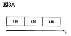
図3A、図3B、図3Cは、半導体装置の動作を説明するための図である。
図4A、図4Bは、半導体装置の構成例を示すフロー図および回路図である。
図5A、図5Bは、半導体装置の構成例を示すフロー図および回路図である。
図6A、図6Bは、半導体装置の構成例を示す回路図である。
図7は、半導体装置の構成例を示すフロー図である。
図8A、図8Bは、半導体装置の構成例を示すフロー図および回路図である。
図9A、図9Bは、半導体装置の構成例を示すフロー図および回路図である。
図10A、図10Bは、半導体装置の構成例を示す模式図である。
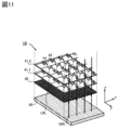
図11は、半導体装置の構成例を示す模式図である。
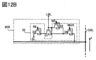
図12A、図12Bは、半導体装置の構成例を示す回路図である。
図13A、図13Bは、半導体装置の構成例を示すブロック図および回路図である。
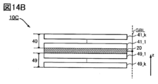
図14A、図14Bは、半導体装置の構成例を示すブロック図である。
図15A、図15B、図15C、図15Dは、半導体装置の構成例を説明するための回路図である。
図16A、図16Bは、半導体装置の構成例を説明するための回路図である。
図17は、半導体装置の構成例を説明するための回路図である。
図18は、半導体装置の構成例を説明するためのタイミングチャートである。
図19A、図19B、図19Cは、半導体装置の構成例を説明するための回路図およびタイミングチャートである。
図20は、半導体装置の構成例を説明するためのタイミングチャートである。
図21は、半導体装置の構成例を示す断面模式図である。
図22A、図22Bは、半導体装置の構成例を示す断面模式図である。
図23A、図23B、図23Cは、半導体装置の構成例を示す断面模式図である。
図24は、半導体装置の構成例を示す断面模式図である。
図25は、半導体装置の構成例を示す断面模式図である。
図26A、図26B、図26Cは、半導体装置の構成例を示す上面図および断面模式図である。
図27A、図27B、図27C、図27Dは、半導体装置の構成例を説明するための上面図である。
図28A、図28B、図28Cは、IGZOの結晶構造の分類を説明する図、石英ガラスのXRDスペクトルを説明する図、結晶性IGZOのXRDスペクトルを説明する図である。
図29は、半導体装置の構成例を説明するブロック図である。
図30は、半導体装置の構成例を示す概念図である。
図31A、図31Bは、電子部品の一例を説明する模式図である。
図32は、電子機器の例を示す図である。
本発明の一態様である半導体装置の構成例について、図1乃至図18を参照して説明する。
以下では、本発明の一態様に係る記憶装置として機能する半導体装置の一例について説明する。
そこで、外部からの不純物混入を抑制するために、不純物の拡散を抑制する材料(以下、不純物に対するバリア性材料ともいう)を用いて、トランジスタ200を封止するとよい。
図22Aを用いて、トランジスタ層413が有するトランジスタ200T、およびメモリデバイス420が有するトランジスタ200Mに用いることができるトランジスタ200について説明する。
酸化物230として、酸化物半導体として機能する金属酸化物を用いることが好ましい。以下では、本発明に係る酸化物230に適用可能な金属酸化物について説明する。
図22Bを用いてトランジスタ300を説明する。トランジスタ300は、半導体基板311上に設けられ、ゲートとして機能する導電体316、ゲート絶縁体として機能する絶縁体315、半導体基板311の一部からなる半導体領域313、およびソース領域またはドレイン領域として機能する低抵抗領域314a、および低抵抗領域314bを有する。トランジスタ300は、pチャネル型、あるいはnチャネル型のいずれでもよい。
次に、図21に示すメモリデバイス420について説明する。なお、メモリデバイス420が有するトランジスタ200Mについて、トランジスタ200と重複する説明は省略する。
次に、図23Bを用いて、メモリデバイス420の変形例として、メモリデバイス420Aを説明する。メモリデバイス420Aは、トランジスタ200Mと、トランジスタ200Mと電気的に接続する容量素子292Aを有する。容量素子292Aは、トランジスタ200Mの下方に設けられる。
次に、図23Cを用いて、メモリデバイス420の変形例として、メモリデバイス420Bを説明する。メモリデバイス420Bは、トランジスタ200Mと、トランジスタ200Mと電気的に接続する容量素子292Bを有する。容量素子292Bは、トランジスタ200Mの上方に設けられる。
図21において一点鎖線で囲んだ領域422にて、メモリデバイス420は、導電体424および導電体205を介してトランジスタ200Tのゲートと電気的に接続されているが、本実施の形態はこれに限らない。


本実施の形態では、上記の実施の形態で説明したOSトランジスタに用いることができる金属酸化物であるCAC-OS(Cloud-Aligned Composite Oxide Semiconductor)、およびCAAC-OS(c-axis Aligned Crystal Oxide Semiconductor)の構成について説明する。
CAC-OSまたはCAC-metal oxideとは、材料の一部では導電性の機能と、材料の一部では絶縁性の機能とを有し、材料の全体では半導体としての機能を有する。なお、CAC-OSまたはCAC-metal oxideを、トランジスタの活性層に用いる場合、導電性の機能は、キャリアとなる電子(またはホール)を流す機能であり、絶縁性の機能は、キャリアとなる電子を流さない機能である。導電性の機能と、絶縁性の機能とを、それぞれ相補的に作用させることで、スイッチングさせる機能(On/Offさせる機能)をCAC-OSまたはCAC-metal oxideに付与することができる。CAC-OSまたはCAC-metal oxideにおいて、それぞれの機能を分離させることで、双方の機能を最大限に高めることができる。
酸化物半導体は、単結晶酸化物半導体と、それ以外の非単結晶酸化物半導体と、に分けられる。非単結晶酸化物半導体としては、例えば、CAAC-OS(c-axis aligned crystalline oxide semiconductor)、多結晶酸化物半導体、nc-OS(nanocrystalline oxide semiconductor)、擬似非晶質酸化物半導体(a-like OS:amorphous-like oxide semiconductor)および非晶質酸化物半導体などがある。
続いて、上記酸化物半導体をトランジスタに用いる場合について説明する。
ここで、酸化物半導体中における各不純物の影響について説明する。
本実施の形態では、実施の形態1に記載の半導体装置10におけるシリコン基板50に設けられたコントロールロジック回路61、行駆動回路62、列駆動回路63および出力回路64について説明する。
本実施の形態は、上記実施の形態に示す半導体装置などが組み込まれた電子部品および電子機器の一例を示す。
まず、半導体装置10等が組み込まれた電子部品の例を、図31Aおよび図31Bを用いて説明を行う。
次に、上記電子部品を備えた電子機器の例について図32を用いて説明を行う。
以上の実施の形態、および実施の形態における各構成の説明について、以下に付記する。
Claims (10)
- シリコン基板をチャネルに用いたトランジスタを複数有する駆動回路と、
金属酸化物をチャネルに用いたトランジスタを複数有する第1トランジスタ層および第2トランジスタ層と、を有し、
前記第1トランジスタ層および前記第2トランジスタ層は、前記シリコン基板上に設けられ、
前記第1トランジスタ層は、第1トランジスタおよび第1キャパシタを有する第1メモリセルを有し、
前記第1トランジスタは、第1ローカルビット線に電気的に接続され、
前記第2トランジスタ層は、ゲートが前記第1ローカルビット線に電気的に接続された第2トランジスタと、前記第2トランジスタに電気的に接続された第1補正回路と、を有し、
前記第1補正回路は、第1グローバルビット線に電気的に接続され、
前記第1補正回路は、前記第2トランジスタのしきい値電圧に応じた電圧を前記第2トランジスタのゲートに保持させる機能を有する、半導体装置。 - シリコン基板をチャネルに用いたトランジスタを複数有する駆動回路と、
複数のトランジスタ層が積層して設けられる素子層と、を有し、
前記素子層は、金属酸化物をチャネルに用いたトランジスタを複数有する第1トランジスタ層および第2トランジスタ層と、を有し、
前記第1トランジスタ層および前記第2トランジスタ層は、前記シリコン基板上に設けられ、
前記第1トランジスタ層は、第1トランジスタおよび第1キャパシタを有する第1メモリセルを有し、
前記第1トランジスタは、第1ローカルビット線に電気的に接続され、
前記第2トランジスタ層は、ゲートが前記第1ローカルビット線に電気的に接続された第2トランジスタと、前記第2トランジスタに電気的に接続された第1補正回路と、を有し、
前記第1補正回路は、第1グローバルビット線に電気的に接続され、
前記第1補正回路は、前記第2トランジスタのしきい値電圧に応じた電圧を前記第2トランジスタのゲートに保持させる機能を有する、半導体装置。 - 請求項1または2において、
前記第1ローカルビット線は、前記シリコン基板の表面に対して垂直方向または概略垂直方向に設けられる、半導体装置。 - 請求項1乃至3のいずれか一において、
前記第1グローバルビット線は、前記第1補正回路と前記駆動回路とを電気的に接続する機能を有する、半導体装置。 - 請求項4において、
前記第1グローバルビット線は、前記シリコン基板の表面に対して垂直方向または概略垂直方向に設けられる、半導体装置。 - 請求項1乃至5のいずれか一において、
前記金属酸化物は、Inと、Gaと、Znと、を含む、半導体装置。 - 請求項1乃至6のいずれか一において、
前記第1補正回路は、第3トランジスタ乃至第5トランジスタを有し、
前記第3トランジスタは、前記第2トランジスタのゲートと、前記第2トランジスタのソースまたはドレインの一方と、の間の導通状態を制御する機能を有し、
前記第4トランジスタは、前記第2トランジスタのソースまたはドレインの他方と、前記第2トランジスタに電流を流すための電位が与えられた配線と、の間の導通状態を制御する機能を有し、
前記第5トランジスタは、前記第2トランジスタのソースまたはドレインの一方と、前記第1グローバルビット線と、の間の導通状態を制御する機能を有する、半導体装置。 - 請求項7において、
前記第1トランジスタは、補正動作を行う期間において、非導通状態にされる、半導体装置。 - 請求項1乃至8のいずれか一において、
第2メモリセルと、第2ローカルビット線と、第2補正回路と、第2グローバルビット線と、第6トランジスタと、第7トランジスタと、第8トランジスタと、を有し、
前記駆動回路は、ビット線対として機能する第1ビット線および第2ビット線に電気的に接続されたセンスアンプを有し、
前記第2メモリセルは、前記第2ローカルビット線に電気的に接続され、
前記第2ローカルビット線は、前記第2補正回路に電気的に接続され、
前記第2補正回路は、前記第2グローバルビット線に電気的に接続され、
前記第6トランジスタは、前記第1ビット線と、前記第1グローバルビット線と、の間の導通状態を制御する機能を有し、
前記第7トランジスタは、前記第2ビット線と、前記第2グローバルビット線と、の間の導通状態を制御する機能を有し、
前記第8トランジスタは、前記第1グローバルビット線と、前記第2グローバルビット線と、の間の導通状態を制御する機能、を有する半導体装置。 - 請求項9において、
前記第6トランジスタ乃至前記第8トランジスタは、金属酸化物をチャネルに用いたトランジスタである、半導体装置。
Priority Applications (1)
| Application Number | Priority Date | Filing Date | Title |
|---|---|---|---|
| JP2024010971A JP2024046762A (ja) | 2019-03-29 | 2024-01-29 | 半導体装置 |
Applications Claiming Priority (9)
| Application Number | Priority Date | Filing Date | Title |
|---|---|---|---|
| JP2019065473 | 2019-03-29 | ||
| JP2019065475 | 2019-03-29 | ||
| JP2019065473 | 2019-03-29 | ||
| JP2019065475 | 2019-03-29 | ||
| JP2019073992 | 2019-04-09 | ||
| JP2019073992 | 2019-04-09 | ||
| JP2019102753 | 2019-05-31 | ||
| JP2019102753 | 2019-05-31 | ||
| PCT/IB2020/052357 WO2020201865A1 (ja) | 2019-03-29 | 2020-03-16 | 半導体装置 |
Related Child Applications (1)
| Application Number | Title | Priority Date | Filing Date |
|---|---|---|---|
| JP2024010971A Division JP2024046762A (ja) | 2019-03-29 | 2024-01-29 | 半導体装置 |
Publications (3)
| Publication Number | Publication Date |
|---|---|
| JPWO2020201865A1 JPWO2020201865A1 (ja) | 2020-10-08 |
| JPWO2020201865A5 JPWO2020201865A5 (ja) | 2023-02-17 |
| JP7429686B2 true JP7429686B2 (ja) | 2024-02-08 |
Family
ID=72666597
Family Applications (2)
| Application Number | Title | Priority Date | Filing Date |
|---|---|---|---|
| JP2021510571A Active JP7429686B2 (ja) | 2019-03-29 | 2020-03-16 | 半導体装置 |
| JP2024010971A Pending JP2024046762A (ja) | 2019-03-29 | 2024-01-29 | 半導体装置 |
Family Applications After (1)
| Application Number | Title | Priority Date | Filing Date |
|---|---|---|---|
| JP2024010971A Pending JP2024046762A (ja) | 2019-03-29 | 2024-01-29 | 半導体装置 |
Country Status (5)
| Country | Link |
|---|---|
| US (1) | US11948626B2 (ja) |
| JP (2) | JP7429686B2 (ja) |
| KR (1) | KR20210142695A (ja) |
| CN (1) | CN113646839A (ja) |
| WO (1) | WO2020201865A1 (ja) |
Families Citing this family (5)
| Publication number | Priority date | Publication date | Assignee | Title |
|---|---|---|---|---|
| WO2023152586A1 (ja) * | 2022-02-10 | 2023-08-17 | 株式会社半導体エネルギー研究所 | 半導体装置、及び半導体装置の作製方法 |
| WO2023156883A1 (ja) * | 2022-02-18 | 2023-08-24 | 株式会社半導体エネルギー研究所 | 半導体装置、及び半導体装置の作製方法 |
| WO2023166374A1 (ja) * | 2022-03-04 | 2023-09-07 | 株式会社半導体エネルギー研究所 | 半導体装置、及び半導体装置の作製方法 |
| US11984165B2 (en) * | 2022-05-24 | 2024-05-14 | Taiwan Semiconductor Manufacturing Company, Ltd. | Memory device with reduced area |
| WO2024047486A1 (ja) * | 2022-09-01 | 2024-03-07 | 株式会社半導体エネルギー研究所 | 記憶装置 |
Citations (2)
| Publication number | Priority date | Publication date | Assignee | Title |
|---|---|---|---|---|
| WO2017055967A1 (en) | 2015-09-30 | 2017-04-06 | Semiconductor Energy Laboratory Co., Ltd. | Semiconductor device and electronic device |
| WO2019003045A1 (ja) | 2017-06-27 | 2019-01-03 | 株式会社半導体エネルギー研究所 | 記憶装置 |
Family Cites Families (17)
| Publication number | Priority date | Publication date | Assignee | Title |
|---|---|---|---|---|
| US5117113A (en) | 1990-07-06 | 1992-05-26 | Thompson And Nielson Electronics Ltd. | Direct reading dosimeter |
| JP3279615B2 (ja) | 1991-04-15 | 2002-04-30 | 株式会社日立製作所 | 半導体装置 |
| JP3248468B2 (ja) | 1997-10-30 | 2002-01-21 | 日本電気株式会社 | 半導体記憶装置 |
| JPH11260054A (ja) | 1998-01-08 | 1999-09-24 | Mitsubishi Electric Corp | ダイナミック型半導体記憶装置 |
| JP4260469B2 (ja) | 2002-12-16 | 2009-04-30 | 株式会社ルネサステクノロジ | 半導体記憶装置 |
| JP5518313B2 (ja) | 2008-08-29 | 2014-06-11 | ピーエスフォー ルクスコ エスエイアールエル | センスアンプ回路及び半導体記憶装置 |
| JP2012256821A (ja) | 2010-09-13 | 2012-12-27 | Semiconductor Energy Lab Co Ltd | 記憶装置 |
| JP2013065638A (ja) * | 2011-09-15 | 2013-04-11 | Elpida Memory Inc | 半導体装置 |
| JP2015041388A (ja) * | 2013-08-20 | 2015-03-02 | 株式会社半導体エネルギー研究所 | 記憶装置、及び半導体装置 |
| US9653611B2 (en) | 2014-03-07 | 2017-05-16 | Semiconductor Energy Laboratory Co., Ltd. | Semiconductor device |
| US10236875B2 (en) * | 2016-04-15 | 2019-03-19 | Semiconductor Energy Laboratory Co., Ltd. | Semiconductor device and method for operating the semiconductor device |
| US10446226B2 (en) | 2016-08-08 | 2019-10-15 | Micron Technology, Inc. | Apparatuses including multi-level memory cells and methods of operation of same |
| US10192871B2 (en) * | 2016-09-23 | 2019-01-29 | Semiconductor Energy Laboratory Co., Ltd. | Semiconductor device |
| US11380688B2 (en) * | 2017-01-27 | 2022-07-05 | Semiconductor Energy Laboratory Co., Ltd. | Capacitor, semiconductor device, and manufacturing method of semiconductor device |
| WO2019048967A1 (ja) | 2017-09-06 | 2019-03-14 | 株式会社半導体エネルギー研究所 | 半導体装置、記憶装置、及び電子機器 |
| JPWO2020245688A1 (ja) * | 2019-06-04 | 2020-12-10 | ||
| JPWO2021234500A1 (ja) * | 2020-05-22 | 2021-11-25 |
-
2020
- 2020-03-16 JP JP2021510571A patent/JP7429686B2/ja active Active
- 2020-03-16 US US17/439,876 patent/US11948626B2/en active Active
- 2020-03-16 KR KR1020217033820A patent/KR20210142695A/ko active Search and Examination
- 2020-03-16 WO PCT/IB2020/052357 patent/WO2020201865A1/ja active Application Filing
- 2020-03-16 CN CN202080025962.6A patent/CN113646839A/zh active Pending
-
2024
- 2024-01-29 JP JP2024010971A patent/JP2024046762A/ja active Pending
Patent Citations (2)
| Publication number | Priority date | Publication date | Assignee | Title |
|---|---|---|---|---|
| WO2017055967A1 (en) | 2015-09-30 | 2017-04-06 | Semiconductor Energy Laboratory Co., Ltd. | Semiconductor device and electronic device |
| WO2019003045A1 (ja) | 2017-06-27 | 2019-01-03 | 株式会社半導体エネルギー研究所 | 記憶装置 |
Also Published As
| Publication number | Publication date |
|---|---|
| US20220180920A1 (en) | 2022-06-09 |
| JPWO2020201865A1 (ja) | 2020-10-08 |
| JP2024046762A (ja) | 2024-04-04 |
| TW202101468A (zh) | 2021-01-01 |
| WO2020201865A1 (ja) | 2020-10-08 |
| US11948626B2 (en) | 2024-04-02 |
| CN113646839A (zh) | 2021-11-12 |
| KR20210142695A (ko) | 2021-11-25 |
Similar Documents
| Publication | Publication Date | Title |
|---|---|---|
| JP7429686B2 (ja) | 半導体装置 | |
| JP7459079B2 (ja) | 半導体装置 | |
| JP7462575B2 (ja) | 半導体装置 | |
| JP7430760B2 (ja) | 記憶装置 | |
| WO2020157553A1 (ja) | 記憶装置 | |
| US11462538B2 (en) | Semiconductor device | |
| CN111373476A (zh) | 存储装置及电子设备 | |
| JP7480113B2 (ja) | 半導体装置および当該半導体装置を有する電気機器 | |
| JP2024036493A (ja) | 半導体装置 | |
| KR20200138305A (ko) | 기억 장치 및 전자 기기 | |
| WO2020170069A1 (ja) | エラー検出機能を有する記憶装置、半導体装置、および、電子機器 | |
| JP7344904B2 (ja) | 半導体装置 | |
| JP7467430B2 (ja) | 記憶装置 |
Legal Events
| Date | Code | Title | Description |
|---|---|---|---|
| A521 | Request for written amendment filed |
Free format text: JAPANESE INTERMEDIATE CODE: A523 Effective date: 20230209 |
|
| A621 | Written request for application examination |
Free format text: JAPANESE INTERMEDIATE CODE: A621 Effective date: 20230209 |
|
| TRDD | Decision of grant or rejection written | ||
| A01 | Written decision to grant a patent or to grant a registration (utility model) |
Free format text: JAPANESE INTERMEDIATE CODE: A01 Effective date: 20240109 |
|
| A61 | First payment of annual fees (during grant procedure) |
Free format text: JAPANESE INTERMEDIATE CODE: A61 Effective date: 20240129 |
|
| R150 | Certificate of patent or registration of utility model |
Ref document number: 7429686 Country of ref document: JP Free format text: JAPANESE INTERMEDIATE CODE: R150 |