JP7429552B2 - 抵抗器及び抵抗器の製造方法 - Google Patents
抵抗器及び抵抗器の製造方法 Download PDFInfo
- Publication number
- JP7429552B2 JP7429552B2 JP2020011196A JP2020011196A JP7429552B2 JP 7429552 B2 JP7429552 B2 JP 7429552B2 JP 2020011196 A JP2020011196 A JP 2020011196A JP 2020011196 A JP2020011196 A JP 2020011196A JP 7429552 B2 JP7429552 B2 JP 7429552B2
- Authority
- JP
- Japan
- Prior art keywords
- resistor
- electrode body
- oxide film
- base material
- electrode
- Prior art date
- Legal status (The legal status is an assumption and is not a legal conclusion. Google has not performed a legal analysis and makes no representation as to the accuracy of the status listed.)
- Active
Links
Images


Classifications
-
- H—ELECTRICITY
- H01—ELECTRIC ELEMENTS
- H01C—RESISTORS
- H01C17/00—Apparatus or processes specially adapted for manufacturing resistors
- H01C17/22—Apparatus or processes specially adapted for manufacturing resistors adapted for trimming
- H01C17/24—Apparatus or processes specially adapted for manufacturing resistors adapted for trimming by removing or adding resistive material
- H01C17/242—Apparatus or processes specially adapted for manufacturing resistors adapted for trimming by removing or adding resistive material by laser
-
- H—ELECTRICITY
- H01—ELECTRIC ELEMENTS
- H01C—RESISTORS
- H01C1/00—Details
- H01C1/02—Housing; Enclosing; Embedding; Filling the housing or enclosure
- H01C1/034—Housing; Enclosing; Embedding; Filling the housing or enclosure the housing or enclosure being formed as coating or mould without outer sheath
-
- H—ELECTRICITY
- H01—ELECTRIC ELEMENTS
- H01C—RESISTORS
- H01C1/00—Details
- H01C1/14—Terminals or tapping points specially adapted for resistors; Arrangements of terminals or tapping points on resistors
-
- H—ELECTRICITY
- H01—ELECTRIC ELEMENTS
- H01C—RESISTORS
- H01C1/00—Details
- H01C1/14—Terminals or tapping points specially adapted for resistors; Arrangements of terminals or tapping points on resistors
- H01C1/142—Terminals or tapping points specially adapted for resistors; Arrangements of terminals or tapping points on resistors the terminals or tapping points being coated on the resistive element
-
- H—ELECTRICITY
- H01—ELECTRIC ELEMENTS
- H01C—RESISTORS
- H01C1/00—Details
- H01C1/14—Terminals or tapping points specially adapted for resistors; Arrangements of terminals or tapping points on resistors
- H01C1/144—Terminals or tapping points specially adapted for resistors; Arrangements of terminals or tapping points on resistors the terminals or tapping points being welded or soldered
-
- H—ELECTRICITY
- H01—ELECTRIC ELEMENTS
- H01C—RESISTORS
- H01C13/00—Resistors not provided for elsewhere
-
- H—ELECTRICITY
- H01—ELECTRIC ELEMENTS
- H01C—RESISTORS
- H01C17/00—Apparatus or processes specially adapted for manufacturing resistors
- H01C17/006—Apparatus or processes specially adapted for manufacturing resistors adapted for manufacturing resistor chips
-
- H—ELECTRICITY
- H01—ELECTRIC ELEMENTS
- H01C—RESISTORS
- H01C17/00—Apparatus or processes specially adapted for manufacturing resistors
- H01C17/28—Apparatus or processes specially adapted for manufacturing resistors adapted for applying terminals
-
- H—ELECTRICITY
- H01—ELECTRIC ELEMENTS
- H01C—RESISTORS
- H01C17/00—Apparatus or processes specially adapted for manufacturing resistors
- H01C17/28—Apparatus or processes specially adapted for manufacturing resistors adapted for applying terminals
- H01C17/281—Apparatus or processes specially adapted for manufacturing resistors adapted for applying terminals by thick film techniques
-
- H—ELECTRICITY
- H01—ELECTRIC ELEMENTS
- H01C—RESISTORS
- H01C7/00—Non-adjustable resistors formed as one or more layers or coatings; Non-adjustable resistors made from powdered conducting material or powdered semi-conducting material with or without insulating material
- H01C7/003—Thick film resistors
Landscapes
- Engineering & Computer Science (AREA)
- Microelectronics & Electronic Packaging (AREA)
- Manufacturing & Machinery (AREA)
- Physics & Mathematics (AREA)
- Optics & Photonics (AREA)
- Plasma & Fusion (AREA)
- Electromagnetism (AREA)
- Details Of Resistors (AREA)
- Non-Adjustable Resistors (AREA)
- Apparatuses And Processes For Manufacturing Resistors (AREA)
Description
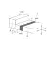
本発明の本実施形態の抵抗器1について、図1、図2を用いて詳細に説明する。図1は、本実施形態の抵抗器1の斜視図である。図2は、本実施形態の抵抗器1を回路基板への実装面側から見た斜視図である。
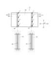
図3は、本実施形態の抵抗器1に形成された酸化膜5(5a)を示す図である。図4は、本実施形態の抵抗器1に形成された酸化膜5(5b)の第1変形例を示す図である。図5は、本実施形態の抵抗器1に形成された酸化膜5(5c)の第2変形例を示す図である。図6は、本実施形態の抵抗器1に形成された酸化膜5(5d)の第3変形例を示す図である。
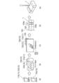
図8は、本実施形態の抵抗器1にトリミングを行う場合の模式図である。図9は、トリミング後の抵抗器1の実装面を示す図である。図10は、トリミング後の抵抗器1の側面図である。
図11は、本実施形態の抵抗器1の変形例を示す図である。本実施形態の抵抗器1の変形例は、第1電極体11の脚部22、第2電極体12の脚部32がなく、抵抗器1の実装面が平坦となっている。一方、回路基板7には電極71,72が配置され、電極71,72は、回路基板7から突出するように配置されている。電極71には第1電極体11が半田(不図示)により実装されており、電極72には第2電極体12が半田(不図示)により実装されている。このとき、抵抗体10は、回路基板7から離間して配置されている。
次に、本実施形態による作用効果について説明する。
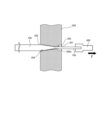
図12は、本実施形態の抵抗器1の製造方法を説明する模式図である。
次に、本実施形態の作用効果について説明する。
10 抵抗体
11 第1電極体
12 第2電極体
13 接合部
14 接合部
5 酸化膜
Claims (6)
- 抵抗体と、前記抵抗体に接続された一対の電極と、を備え、基板に実装した場合に少なくとも前記抵抗体が前記基板から離間して配置される抵抗器であって、
抵抗器の実装面の前記抵抗体と前記電極との境界部位のうち、前記抵抗体及び前記電極の少なくとも一方の表面に、それぞれの材料の酸化による酸化膜を有し、
前記抵抗器の前記実装面において、前記抵抗体及び前記電極の少なくとも一方に形成された前記酸化膜の部位を除き、前記抵抗体の表面が露出している、
抵抗器。 - 請求項1に記載の抵抗器であって、
前記酸化膜は、少なくとも前記抵抗体に形成されている抵抗器。 - 請求項1又は2に記載の抵抗器において、
前記電極は、前記抵抗体に接続する胴体部と、前記基板の方向に突出した脚部と、を有するとともに前記抵抗体と前記胴体部により前記境界部位が形成され、
前記酸化膜は、前記抵抗体と前記胴体部との前記境界部位のうち、少なくとも前記胴体部に形成されている抵抗器。 - 請求項1乃至3のいずれか1項に記載の抵抗器であって、
前記境界部位において、凹部を有し、
前記酸化膜は前記凹部に形成されている抵抗器。 - 請求項3に記載の抵抗器であって、
前記境界部位において、凹部を有し、
前記酸化膜は前記凹部に形成され、前記凹部は、前記胴体部と前記抵抗体の双方に亘って形成されている抵抗器。 - 抵抗体と、前記抵抗体に接続された一対の電極と、を備え、基板に実装した時に少なくとも前記抵抗体が前記基板から離間して配置される抵抗器の製造方法であって、
抵抗器の実装面における前記抵抗体と前記電極との境界部位のうち前記抵抗体及び前記電極の少なくとも一方の表面にレーザを照射して、それぞれの材料の酸化による酸化膜を形成する工程を有し、
前記抵抗器の前記実装面において、前記抵抗体及び前記電極の少なくとも一方に形成された前記酸化膜の部位を除き、前記抵抗体の表面が露出している前記酸化膜を形成する、
抵抗器の製造方法。
Priority Applications (3)
| Application Number | Priority Date | Filing Date | Title |
|---|---|---|---|
| JP2020011196A JP7429552B2 (ja) | 2020-01-27 | 2020-01-27 | 抵抗器及び抵抗器の製造方法 |
| US17/759,506 US12249448B2 (en) | 2020-01-27 | 2020-12-28 | Resistor and manufacturing method of resistor |
| PCT/JP2020/049195 WO2021153152A1 (ja) | 2020-01-27 | 2020-12-28 | 抵抗器、及び抵抗器の製造方法 |
Applications Claiming Priority (1)
| Application Number | Priority Date | Filing Date | Title |
|---|---|---|---|
| JP2020011196A JP7429552B2 (ja) | 2020-01-27 | 2020-01-27 | 抵抗器及び抵抗器の製造方法 |
Publications (2)
| Publication Number | Publication Date |
|---|---|
| JP2021118280A JP2021118280A (ja) | 2021-08-10 |
| JP7429552B2 true JP7429552B2 (ja) | 2024-02-08 |
Family
ID=77078527
Family Applications (1)
| Application Number | Title | Priority Date | Filing Date |
|---|---|---|---|
| JP2020011196A Active JP7429552B2 (ja) | 2020-01-27 | 2020-01-27 | 抵抗器及び抵抗器の製造方法 |
Country Status (3)
| Country | Link |
|---|---|
| US (1) | US12249448B2 (ja) |
| JP (1) | JP7429552B2 (ja) |
| WO (1) | WO2021153152A1 (ja) |
Families Citing this family (2)
| Publication number | Priority date | Publication date | Assignee | Title |
|---|---|---|---|---|
| JP7429552B2 (ja) * | 2020-01-27 | 2024-02-08 | Koa株式会社 | 抵抗器及び抵抗器の製造方法 |
| JP7627591B2 (ja) * | 2021-03-25 | 2025-02-06 | Koa株式会社 | 抵抗器及び抵抗器の製造方法 |
Citations (4)
| Publication number | Priority date | Publication date | Assignee | Title |
|---|---|---|---|---|
| JP2002075714A (ja) | 2000-08-24 | 2002-03-15 | Koa Corp | 低抵抗器及びその製造方法 |
| JP2004071692A (ja) | 2002-08-02 | 2004-03-04 | Koa Corp | 抵抗器 |
| JP2013089664A (ja) | 2011-10-14 | 2013-05-13 | Rohm Co Ltd | チップ抵抗器、チップ抵抗器の実装構造、およびチップ抵抗器の製造方法 |
| JP2015065197A (ja) | 2013-09-24 | 2015-04-09 | コーア株式会社 | ジャンパー素子または電流検出用抵抗素子 |
Family Cites Families (4)
| Publication number | Priority date | Publication date | Assignee | Title |
|---|---|---|---|---|
| JP2009071123A (ja) | 2007-09-14 | 2009-04-02 | Rohm Co Ltd | チップ抵抗器の製造方法 |
| JP5417572B2 (ja) * | 2008-02-22 | 2014-02-19 | ヴィシェイ アドバンスト テクノロジーズ リミテッド | チップ抵抗器とその製造方法 |
| JP5778690B2 (ja) * | 2010-11-22 | 2015-09-16 | Tdk株式会社 | チップサーミスタ及びサーミスタ集合基板 |
| JP7429552B2 (ja) * | 2020-01-27 | 2024-02-08 | Koa株式会社 | 抵抗器及び抵抗器の製造方法 |
-
2020
- 2020-01-27 JP JP2020011196A patent/JP7429552B2/ja active Active
- 2020-12-28 WO PCT/JP2020/049195 patent/WO2021153152A1/ja not_active Ceased
- 2020-12-28 US US17/759,506 patent/US12249448B2/en active Active
Patent Citations (4)
| Publication number | Priority date | Publication date | Assignee | Title |
|---|---|---|---|---|
| JP2002075714A (ja) | 2000-08-24 | 2002-03-15 | Koa Corp | 低抵抗器及びその製造方法 |
| JP2004071692A (ja) | 2002-08-02 | 2004-03-04 | Koa Corp | 抵抗器 |
| JP2013089664A (ja) | 2011-10-14 | 2013-05-13 | Rohm Co Ltd | チップ抵抗器、チップ抵抗器の実装構造、およびチップ抵抗器の製造方法 |
| JP2015065197A (ja) | 2013-09-24 | 2015-04-09 | コーア株式会社 | ジャンパー素子または電流検出用抵抗素子 |
Also Published As
| Publication number | Publication date |
|---|---|
| WO2021153152A1 (ja) | 2021-08-05 |
| US20230040165A1 (en) | 2023-02-09 |
| US12249448B2 (en) | 2025-03-11 |
| JP2021118280A (ja) | 2021-08-10 |
Similar Documents
| Publication | Publication Date | Title |
|---|---|---|
| CN107710349A (zh) | 电阻器及其制造方法 | |
| JP6650409B2 (ja) | 電流検出用抵抗器 | |
| US8368502B2 (en) | Surface-mount current fuse | |
| JP7429552B2 (ja) | 抵抗器及び抵抗器の製造方法 | |
| JPWO1999018584A1 (ja) | 低抵抗抵抗器およびその製造方法 | |
| CN102640233A (zh) | 分流电阻器及其制造方法 | |
| WO2014038372A1 (ja) | 電流検出用抵抗器 | |
| JP2009218552A (ja) | チップ抵抗器およびその製造方法 | |
| WO2018150869A1 (ja) | 電流測定装置および電流検出用抵抗器 | |
| WO2019097925A1 (ja) | シャント抵抗器 | |
| US20200243228A1 (en) | Method for manufacturing resistor | |
| JP2024161111A (ja) | シャント抵抗器 | |
| JP2024144722A (ja) | 抵抗器 | |
| WO2021153153A1 (ja) | 抵抗器の製造方法、及び抵抗器 | |
| CN100481277C (zh) | 分流电阻器及其制造方法 | |
| JP7421416B2 (ja) | 抵抗器 | |
| JP7075297B2 (ja) | シャント装置 | |
| JP2022123429A (ja) | シャント抵抗器と電圧信号検出基板との接続方法、および電流検出装置 | |
| US20100012374A1 (en) | Welding method and welding structure of conductive terminals | |
| JP2019165057A (ja) | シャント抵抗器及びその製造方法 | |
| WO2025100035A1 (ja) | 抵抗器の製造方法 | |
| CN117716452A (zh) | 基板内置用的芯片型电阻器、电阻器内置模块及其制造方法、修剪方法 | |
| JP2004319874A (ja) | チップ抵抗器およびその製造方法 | |
| JP2024094050A (ja) | 固定抵抗器 | |
| JP2013254983A (ja) | チップ抵抗器およびその製造方法 |
Legal Events
| Date | Code | Title | Description |
|---|---|---|---|
| A621 | Written request for application examination |
Free format text: JAPANESE INTERMEDIATE CODE: A621 Effective date: 20221221 |
|
| A131 | Notification of reasons for refusal |
Free format text: JAPANESE INTERMEDIATE CODE: A131 Effective date: 20230711 |
|
| A521 | Request for written amendment filed |
Free format text: JAPANESE INTERMEDIATE CODE: A523 Effective date: 20230908 |
|
| A131 | Notification of reasons for refusal |
Free format text: JAPANESE INTERMEDIATE CODE: A131 Effective date: 20231003 |
|
| A521 | Request for written amendment filed |
Free format text: JAPANESE INTERMEDIATE CODE: A523 Effective date: 20231129 |
|
| TRDD | Decision of grant or rejection written | ||
| A01 | Written decision to grant a patent or to grant a registration (utility model) |
Free format text: JAPANESE INTERMEDIATE CODE: A01 Effective date: 20240123 |
|
| A61 | First payment of annual fees (during grant procedure) |
Free format text: JAPANESE INTERMEDIATE CODE: A61 Effective date: 20240129 |
|
| R150 | Certificate of patent or registration of utility model |
Ref document number: 7429552 Country of ref document: JP Free format text: JAPANESE INTERMEDIATE CODE: R150 |