JP7429552B2 - Resistor and resistor manufacturing method - Google Patents

Resistor and resistor manufacturing method Download PDF

Info

Publication number
JP7429552B2
JP7429552B2 JP2020011196A JP2020011196A JP7429552B2 JP 7429552 B2 JP7429552 B2 JP 7429552B2 JP 2020011196 A JP2020011196 A JP 2020011196A JP 2020011196 A JP2020011196 A JP 2020011196A JP 7429552 B2 JP7429552 B2 JP 7429552B2
Authority
JP
Japan
Prior art keywords
resistor
electrode body
oxide film
base material
electrode
Prior art date
Legal status (The legal status is an assumption and is not a legal conclusion. Google has not performed a legal analysis and makes no representation as to the accuracy of the status listed.)
Active
Application number
JP2020011196A
Other languages
Japanese (ja)
Other versions
JP2021118280A (en
Inventor
航児 江藤
陽平 常盤
玲那 金子
純平 山本
Current Assignee (The listed assignees may be inaccurate. Google has not performed a legal analysis and makes no representation or warranty as to the accuracy of the list.)
Koa Corp
Original Assignee
Koa Corp
Priority date (The priority date is an assumption and is not a legal conclusion. Google has not performed a legal analysis and makes no representation as to the accuracy of the date listed.)
Filing date
Publication date
Application filed by Koa Corp filed Critical Koa Corp
Priority to JP2020011196A priority Critical patent/JP7429552B2/en
Priority to PCT/JP2020/049195 priority patent/WO2021153152A1/en
Priority to US17/759,506 priority patent/US20230040165A1/en
Publication of JP2021118280A publication Critical patent/JP2021118280A/en
Application granted granted Critical
Publication of JP7429552B2 publication Critical patent/JP7429552B2/en
Active legal-status Critical Current
Anticipated expiration legal-status Critical

Links

Images

Classifications

    • HELECTRICITY
    • H01ELECTRIC ELEMENTS
    • H01CRESISTORS
    • H01C17/00Apparatus or processes specially adapted for manufacturing resistors
    • H01C17/22Apparatus or processes specially adapted for manufacturing resistors adapted for trimming
    • H01C17/24Apparatus or processes specially adapted for manufacturing resistors adapted for trimming by removing or adding resistive material
    • H01C17/242Apparatus or processes specially adapted for manufacturing resistors adapted for trimming by removing or adding resistive material by laser
    • HELECTRICITY
    • H01ELECTRIC ELEMENTS
    • H01CRESISTORS
    • H01C1/00Details
    • H01C1/02Housing; Enclosing; Embedding; Filling the housing or enclosure
    • H01C1/034Housing; Enclosing; Embedding; Filling the housing or enclosure the housing or enclosure being formed as coating or mould without outer sheath
    • HELECTRICITY
    • H01ELECTRIC ELEMENTS
    • H01CRESISTORS
    • H01C1/00Details
    • H01C1/14Terminals or tapping points or electrodes specially adapted for resistors; Arrangements of terminals or tapping points or electrodes on resistors
    • HELECTRICITY
    • H01ELECTRIC ELEMENTS
    • H01CRESISTORS
    • H01C1/00Details
    • H01C1/14Terminals or tapping points or electrodes specially adapted for resistors; Arrangements of terminals or tapping points or electrodes on resistors
    • H01C1/142Terminals or tapping points or electrodes specially adapted for resistors; Arrangements of terminals or tapping points or electrodes on resistors the terminals or tapping points being coated on the resistive element
    • HELECTRICITY
    • H01ELECTRIC ELEMENTS
    • H01CRESISTORS
    • H01C1/00Details
    • H01C1/14Terminals or tapping points or electrodes specially adapted for resistors; Arrangements of terminals or tapping points or electrodes on resistors
    • H01C1/144Terminals or tapping points or electrodes specially adapted for resistors; Arrangements of terminals or tapping points or electrodes on resistors the terminals or tapping points being welded or soldered
    • HELECTRICITY
    • H01ELECTRIC ELEMENTS
    • H01CRESISTORS
    • H01C13/00Resistors not provided for elsewhere
    • HELECTRICITY
    • H01ELECTRIC ELEMENTS
    • H01CRESISTORS
    • H01C17/00Apparatus or processes specially adapted for manufacturing resistors
    • H01C17/006Apparatus or processes specially adapted for manufacturing resistors adapted for manufacturing resistor chips
    • HELECTRICITY
    • H01ELECTRIC ELEMENTS
    • H01CRESISTORS
    • H01C17/00Apparatus or processes specially adapted for manufacturing resistors
    • H01C17/28Apparatus or processes specially adapted for manufacturing resistors adapted for applying terminals
    • HELECTRICITY
    • H01ELECTRIC ELEMENTS
    • H01CRESISTORS
    • H01C17/00Apparatus or processes specially adapted for manufacturing resistors
    • H01C17/28Apparatus or processes specially adapted for manufacturing resistors adapted for applying terminals
    • H01C17/281Apparatus or processes specially adapted for manufacturing resistors adapted for applying terminals by thick film techniques
    • HELECTRICITY
    • H01ELECTRIC ELEMENTS
    • H01CRESISTORS
    • H01C7/00Non-adjustable resistors formed as one or more layers or coatings; Non-adjustable resistors made from powdered conducting material or powdered semi-conducting material with or without insulating material
    • H01C7/003Thick film resistors

Landscapes

  • Engineering & Computer Science (AREA)
  • Microelectronics & Electronic Packaging (AREA)
  • Manufacturing & Machinery (AREA)
  • Physics & Mathematics (AREA)
  • Optics & Photonics (AREA)
  • Plasma & Fusion (AREA)
  • Electromagnetism (AREA)
  • Non-Adjustable Resistors (AREA)
  • Details Of Resistors (AREA)
  • Apparatuses And Processes For Manufacturing Resistors (AREA)

Description

本発明は、抵抗器及び抵抗器の製造方法に関する。 The present invention relates to a resistor and a method of manufacturing the resistor.

特許文献1は、電流検出用の抵抗器として、抵抗体の両端面に一対の電極を溶接した抵抗器を開示している。 Patent Document 1 discloses, as a resistor for current detection, a resistor in which a pair of electrodes are welded to both end surfaces of a resistor.

特開2009-071123号公報JP2009-071123A

特許文献1に係るタイプの抵抗器では、抵抗体と基板との間隔が狭くなると、リフロー工程において半田が電極を伝って抵抗体にまで這い上がり、電流の検出精度が低下する虞が顕著となる。もちろん、抵抗体表面を樹脂で覆うことで半田が抵抗体に接触しないようにすることも可能であるが、製造歩留まりの低下及び製造コストの上昇を引き起こす。 In the type of resistor disclosed in Patent Document 1, if the distance between the resistor and the substrate becomes narrow, there is a significant risk that solder will creep up to the resistor through the electrodes during the reflow process, reducing current detection accuracy. . Of course, it is possible to prevent the solder from coming into contact with the resistor by covering the surface of the resistor with resin, but this causes a decrease in manufacturing yield and an increase in manufacturing cost.

そこで本発明は、簡易な構成で抵抗体への半田の這い上がりを阻止可能な抵抗器、及び抵抗器の製造方法を提供することを目的とする。 SUMMARY OF THE INVENTION Therefore, an object of the present invention is to provide a resistor that can prevent solder from creeping up onto a resistor with a simple configuration, and a method for manufacturing the resistor.

本発明の1つの態様によれば、抵抗体と、前記抵抗体に接続された一対の電極と、を備え、基板に実装した場合に少なくとも前記抵抗体が前記基板から離間して配置される抵抗器であって、抵抗器の実装面の前記抵抗体と前記電極との境界部位のうち、前記抵抗体及び前記電極の少なくとも一方の表面に、それぞれの材料の酸化による酸化膜を有し、前記抵抗器の前記実装面において、前記抵抗体及び前記電極の少なくとも一方に形成された前記酸化膜の部位を除き、前記抵抗体の表面が露出している、抵抗器が提供される。
According to one aspect of the present invention, the resistor includes a resistor and a pair of electrodes connected to the resistor, and when mounted on a substrate, at least the resistor is disposed apart from the substrate. The resistor has an oxide film formed by oxidation of each material on a surface of at least one of the resistor and the electrode in a boundary area between the resistor and the electrode on a mounting surface of the resistor, A resistor is provided, in which the surface of the resistor is exposed on the mounting surface of the resistor except for a portion of the oxide film formed on at least one of the resistor and the electrode.

本発明の1つの態様によれば、酸化膜は半田に対する濡れ性が低い。よって、抵抗体と基板との間隔が狭くなっても半田が酸化膜に這い上がりにくくなるので、半田が酸化膜を超えて抵抗体まで這い上がることを阻止できる。したがって、抵抗体を樹脂で覆う場合に比べて、製造歩留まりを高め、且つ製造コストを抑制することができる。 According to one aspect of the present invention, the oxide film has low wettability to solder. Therefore, even if the distance between the resistor and the substrate becomes narrow, it becomes difficult for the solder to creep up onto the oxide film, so that the solder can be prevented from climbing up beyond the oxide film to the resistor. Therefore, compared to the case where the resistor is covered with resin, manufacturing yield can be increased and manufacturing costs can be reduced.

図1は、本実施形態の抵抗器の斜視図である。FIG. 1 is a perspective view of the resistor of this embodiment. 図2は、本実施形態の抵抗器を回路基板への実装面側から見た斜視図である。FIG. 2 is a perspective view of the resistor of this embodiment viewed from the side where it is mounted on a circuit board. 図3は、本実施形態の抵抗器に形成された酸化膜を示す図である。FIG. 3 is a diagram showing an oxide film formed on the resistor of this embodiment. 図4は、本実施形態の抵抗器に形成された酸化膜の第1変形例を示す図である。FIG. 4 is a diagram showing a first modification of the oxide film formed on the resistor of this embodiment. 図5は、本実施形態の抵抗器に形成された酸化膜の第2変形例を示す図である。FIG. 5 is a diagram showing a second modification of the oxide film formed on the resistor of this embodiment. 図6は、本実施形態の抵抗器に形成された酸化膜の第3変形例を示す図である。FIG. 6 is a diagram showing a third modification of the oxide film formed on the resistor of this embodiment. 図7は、本実施形態の抵抗器を半田実装したときの断面写真である。FIG. 7 is a cross-sectional photograph of the resistor of this embodiment when it is soldered-mounted. 図8は、本実施形態の抵抗器にトリミングを行う場合の模式図である。FIG. 8 is a schematic diagram when trimming the resistor of this embodiment. 図9は、トリミング後の抵抗器の実装面を示す図である。FIG. 9 is a diagram showing the mounting surface of the resistor after trimming. 図10は、トリミング後の抵抗器の側面図である。FIG. 10 is a side view of the resistor after trimming. 図11は、本実施形態の抵抗器の変形例を示す図である。FIG. 11 is a diagram showing a modification of the resistor of this embodiment. 図12は、本実施形態の抵抗器の製造方法を説明する模式図である。FIG. 12 is a schematic diagram illustrating the method for manufacturing the resistor of this embodiment. 図13は、図12に示す工程(c)に用いられるダイスを引き抜き方向Fの上流側から見た正面図である。FIG. 13 is a front view of the die used in step (c) shown in FIG. 12, viewed from the upstream side in the drawing direction F. 図14は、図13のB-B線断面図であって、本実施形態の抵抗器の製造方法における形状を加工する工程を説明する模式図である。FIG. 14 is a cross-sectional view taken along the line BB in FIG. 13, and is a schematic diagram illustrating a step of processing the shape in the resistor manufacturing method of this embodiment.

[抵抗器の説明]
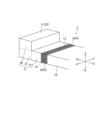
本発明の本実施形態の抵抗器1について、図1、図2を用いて詳細に説明する。図1は、本実施形態の抵抗器1の斜視図である。図2は、本実施形態の抵抗器1を回路基板への実装面側から見た斜視図である。
[Resistor description]
The resistor 1 of this embodiment of the present invention will be explained in detail using FIGS. 1 and 2. FIG. 1 is a perspective view of a resistor 1 of this embodiment. FIG. 2 is a perspective view of the resistor 1 of this embodiment viewed from the side where it is mounted on a circuit board.

抵抗器1は、抵抗体10と、第1電極体11(電極)と、第2電極体12(電極)とを備え、第1電極体11と抵抗体10と第2電極体12とが、この順に接合されたものである。抵抗器1は、図1には示されていない回路基板等に実装される。例えば、抵抗器1は、回路基板のランドパターン上に形成された一対の電極の上に配置される。本実施形態では、抵抗器1は、電流検出用抵抗器(シャント抵抗器)として用いられる。 The resistor 1 includes a resistor 10, a first electrode body 11 (electrode), and a second electrode body 12 (electrode), and the first electrode body 11, the resistor 10, and the second electrode body 12 are They are joined in this order. The resistor 1 is mounted on a circuit board or the like that is not shown in FIG. For example, the resistor 1 is placed on a pair of electrodes formed on a land pattern of a circuit board. In this embodiment, the resistor 1 is used as a current detection resistor (shunt resistor).

なお、本実施形態では、第1電極体11と第2電極体12が並ぶ方向(抵抗器1の長手方向)をX方向(第1電極体11側を+X方向、第2電極体12側を-X方向)とし、抵抗器1の幅方向をY方向(図1の紙面手前側を+Y方向、図1の紙面奥側を-Y方向)とし、抵抗器1の厚み方向をZ方向(回路基板に向かう方向を-Z方向、回路基板から離れる方向を+Z方向)とし、X方向、Y方向、Z方向は互いに直交するものとする。また、抵抗器1の実装面とは、回路基板に抵抗器1を実装する際に抵抗器1が回路基板に対向する面を意味し、第1電極体11、抵抗体10、第2電極体12の回路基板に対向する面を含む。 In this embodiment, the direction in which the first electrode body 11 and the second electrode body 12 are lined up (the longitudinal direction of the resistor 1) is the X direction (the first electrode body 11 side is the +X direction, the second electrode body 12 side is the +X direction). -X direction), the width direction of resistor 1 is the Y direction (the front side of the page in Figure 1 is the +Y direction, the back side of the page in Figure 1 is the -Y direction), and the thickness direction of the resistor 1 is the Z direction (circuit The direction toward the circuit board is the -Z direction, and the direction away from the circuit board is the +Z direction), and the X, Y, and Z directions are orthogonal to each other. In addition, the mounting surface of the resistor 1 means the surface of the resistor 1 facing the circuit board when the resistor 1 is mounted on the circuit board, and includes the first electrode body 11, the resistor body 10, and the second electrode body. It includes a surface facing the 12 circuit boards.

本実施形態においては、抵抗体10は、直方体(又は立方体)形状に形成されている。 In this embodiment, the resistor 10 is formed in the shape of a rectangular parallelepiped (or cube).

抵抗体10は、用途に合わせて低抵抗から高抵抗の材料を用いることが可能である。本実施形態において、抵抗体10は、大電流を精度よく検出する観点から、比抵抗が小さく、且つ抵抗温度係数(TCR)が小さい抵抗体材料であることが好ましい。一例として、銅・マンガン・ニッケル系合金、銅・マンガン・スズ系合金、ニッケル・クロム系合金、銅・ニッケル系合金等を使用することができる。 The resistor 10 can be made of a material having a low resistance to a high resistance depending on the purpose. In this embodiment, the resistor 10 is preferably made of a resistor material that has a low specific resistance and a low temperature coefficient of resistance (TCR) from the viewpoint of accurately detecting large currents. As an example, a copper-manganese-nickel alloy, a copper-manganese-tin alloy, a nickel-chromium alloy, a copper-nickel alloy, etc. can be used.

第1電極体11は、抵抗体10に接合する胴体部21と、胴体部21と一体に形成され回路基板側に延びる脚部22とを備える。また、第2電極体12は、抵抗体10に接合する胴体部31と、胴体部31と一体に形成され回路基板側に延びる脚部32と、を備える。 The first electrode body 11 includes a body portion 21 that is joined to the resistor 10, and leg portions 22 that are formed integrally with the body portion 21 and extend toward the circuit board. Further, the second electrode body 12 includes a body portion 31 that is joined to the resistor 10, and leg portions 32 that are formed integrally with the body portion 31 and extend toward the circuit board side.

第1電極体11(胴体部21、脚部22)及び第2電極体12(胴体部31、脚部32)は、安定した検出精度を確保する観点から、電気伝導性及び熱伝導性の良好な導電性材料であることが好ましい。一例として、第1電極体11及び第2電極体12として、銅、銅系合金等を使用することができる。銅の中では、無酸素銅(C1020)を使用することが好ましい。第1電極体11と第2電極体12とは、互いに同一のものを使用できる。 The first electrode body 11 (body part 21, leg part 22) and the second electrode body 12 (body part 31, leg part 32) have good electrical conductivity and thermal conductivity from the viewpoint of ensuring stable detection accuracy. The material is preferably a conductive material. As an example, copper, a copper-based alloy, or the like can be used for the first electrode body 11 and the second electrode body 12. Among coppers, it is preferable to use oxygen-free copper (C1020). The first electrode body 11 and the second electrode body 12 can be the same.

第1電極体11における胴体部21は、抵抗体10の+X方向の端面と略同形状の端面を有し、この端面において抵抗体10の+X方向の端面と突き合わされた態様で接合している。胴体部21と抵抗体10との境界部位である接合部13では、抵抗体10と胴体部21との境界に段差がなく平坦であり、抵抗体10と胴体部21とは滑らかに連続している。すなわち、接合部13の表面は、抵抗体10と胴体部21との境界全周に亘って平坦(段差がない状態)に形成されている。 The body portion 21 of the first electrode body 11 has an end surface having approximately the same shape as the end surface of the resistor 10 in the +X direction, and is joined to the end surface of the resistor 10 in the +X direction in abutted manner at this end surface. . At the joint 13, which is the boundary between the body 21 and the resistor 10, the boundary between the resistor 10 and the body 21 is flat with no step, and the resistor 10 and the body 21 are smoothly connected. There is. That is, the surface of the joint portion 13 is formed flat (with no level difference) over the entire boundary between the resistor 10 and the body portion 21 .

第2電極体12における胴体部31は、抵抗体10の-X方向の端面と略同形状の端面を有し、この端面において抵抗体10の-X方向の端面と突き合わされた態様で接合している。胴体部31と抵抗体10との境界部位である接合部14では、抵抗体10と胴体部31との境界に段差がなく平坦であり、抵抗体10と胴体部31とは滑らかに連続している。すなわち、接合部14の表面は、抵抗体10と胴体部31との境界全周に亘って平坦(段差がない状態)に形成されている。 The body portion 31 of the second electrode body 12 has an end surface having approximately the same shape as the end surface of the resistor 10 in the -X direction, and is joined to the end surface of the resistor 10 in the -X direction in a butted manner at this end surface. ing. At the joint 14, which is the boundary between the body 31 and the resistor 10, the boundary between the resistor 10 and the body 31 is flat with no step, and the resistor 10 and the body 31 are smoothly connected. There is. That is, the surface of the joint portion 14 is formed to be flat (without a step) over the entire boundary between the resistor 10 and the body portion 31.

脚部22は、抵抗器1の実装面、即ち胴体部21の回路基板側から-Z方向に向けて延出した部材である。脚部22は、胴体部21よりもX方向の長さが短くなっているが、+X方向の側面は胴体部21の+X方向の側面と同一平面を形成している。 The leg portion 22 is a member extending in the −Z direction from the mounting surface of the resistor 1, that is, from the circuit board side of the body portion 21. The leg portions 22 have a shorter length in the X direction than the body portion 21, but the side surfaces in the +X direction form the same plane as the side surfaces of the body portion 21 in the +X direction.

脚部32は、抵抗器1の実装面、即ち胴体部31の回路基板側から-Z方向に向けて延出した部材である。脚部32は、胴体部31よりもX方向の長さが短くなっているが、-X方向の側面は胴体部31の-X方向の側面と同一平面を形成している。 The leg portion 32 is a member extending in the −Z direction from the mounting surface of the resistor 1, that is, from the circuit board side of the body portion 31. The leg portions 32 have a shorter length in the X direction than the body portion 31, but the side surfaces in the −X direction form the same plane as the side surfaces of the body portion 31 in the −X direction.

本実施形態において、抵抗体10と第1電極体11との接合部13、及び抵抗体10と第2電極体12との接合部14の各々は、互いにクラッド接合(固相接合)にて接合している。すなわち、接合面の各々は、抵抗体10と第1電極体11の金属原子が互いに拡散した拡散接合面、抵抗体10と第2電極体12の金属原子が互いに拡散した拡散接合面、となっている。 In this embodiment, each of the bonding portion 13 between the resistor 10 and the first electrode body 11 and the bonding portion 14 between the resistor 10 and the second electrode body 12 are bonded to each other by clad bonding (solid phase bonding). are doing. That is, each of the bonding surfaces becomes a diffusion bonding surface where the metal atoms of the resistor 10 and the first electrode body 11 are diffused into each other, and a diffusion bonding surface where the metal atoms of the resistor 10 and the second electrode body 12 are diffused into each other. ing.

抵抗器1は、脚部22及び脚部32が回路基板側に突出するように回路基板上に実装されることにより、抵抗体10が回路基板から離間した状態で回路基板に実装される。 The resistor 1 is mounted on the circuit board so that the legs 22 and 32 protrude toward the circuit board, so that the resistor 10 is mounted on the circuit board with the resistor 10 spaced apart from the circuit board.

胴体部21において-X方向側に突出した部分は突出部211であり、突出部211が抵抗体10に接合している。同様に、胴体部31において+X方向側に突出した部分は突出部311であり、突出部311が抵抗体10に接合している。 A portion of the body portion 21 that protrudes in the -X direction is a protrusion 211, and the protrusion 211 is joined to the resistor 10. Similarly, a portion of the body portion 31 that protrudes in the +X direction is a protrusion 311 , and the protrusion 311 is joined to the resistor 10 .

抵抗器1の長手方向(X方向)の長さL(図1参照)を一定としたとき、突出部211のX方向の長さ(胴体部21の長さ、図1参照)、又は突出部311のX方向の長さ(胴体部31のX方向の長さ、図1)を任意に調整し、抵抗体10のX方向の長さL0(図1参照)をL0=L-(L1+L2)として調整することができる。したがって、抵抗器1の寸法Lを変更することなく、また脚部22,32の形状を変更することなく、抵抗器1の抵抗値を任意に調整することができる。または、抵抗器1の寸法Lを変更することなく、突出部211,311の突出量を大きくしても、脚部22と脚部32との距離を確保することができるため、ランドパターン間距離を確保しつつ、抵抗器1の設計自由度を高くすることができる。 When the length L in the longitudinal direction (X direction) of the resistor 1 (see FIG. 1) is constant, the length in the X direction of the protruding portion 211 (length of the body portion 21, see FIG. 1) or the protruding portion 311 in the X direction (the length of the body part 31 in the X direction, Fig. 1), and the length L0 of the resistor 10 in the X direction (see Fig. 1) is set to L0 = L - (L1 + L2). It can be adjusted as Therefore, the resistance value of the resistor 1 can be arbitrarily adjusted without changing the dimension L of the resistor 1 or the shape of the legs 22, 32. Alternatively, even if the amount of protrusion of the protrusions 211 and 311 is increased without changing the dimension L of the resistor 1, the distance between the legs 22 and 32 can be secured, so the distance between the land patterns While ensuring this, the degree of freedom in designing the resistor 1 can be increased.

ここで、抵抗体10の長手方向(X方向)における抵抗体10の長さL0と、第1電極体11のX方向の長さL1と、第2電極体12のX方向の長さL2の比は、任意に設定することができる。ただし、TCR(抵抗温度係数[ppm/℃])の増加を抑制しつつ、抵抗値を小さくする観点から、L1:L0:L2=1:2:1、若しくは1:2:1近傍であることが好ましい。 Here, the length L0 of the resistor 10 in the longitudinal direction (X direction) of the resistor 10, the length L1 of the first electrode body 11 in the X direction, and the length L2 of the second electrode body 12 in the X direction. The ratio can be set arbitrarily. However, from the viewpoint of reducing the resistance value while suppressing the increase in TCR (temperature coefficient of resistance [ppm/℃]), L1:L0:L2 should be 1:2:1 or around 1:2:1. is preferred.

更に、放熱性を高めるとともに、抵抗値を小さくする観点から、抵抗器1の長さL(=L1+L0+L2)に対する抵抗体10の長さL0の比率は、50%以下であることが好ましい。 Furthermore, from the viewpoint of improving heat dissipation and reducing the resistance value, the ratio of the length L0 of the resistor 10 to the length L (=L1+L0+L2) of the resistor 1 is preferably 50% or less.

本実施形態において、抵抗器1は、表面に、筋状凹凸15(図1(拡大図)、図2(拡大図))を有する。本実施形態においては、筋状凹凸15は、抵抗器1の+Y方向に対向する側面、及び-Y方向に対向する側面以外の側面においてY方向に沿って延びるように形成されている。 In this embodiment, the resistor 1 has streak-like unevenness 15 (FIG. 1 (enlarged view), FIG. 2 (enlarged view)) on the surface. In the present embodiment, the linear unevenness 15 is formed to extend along the Y direction on the side surface of the resistor 1 other than the side surface facing the +Y direction and the side surface facing the −Y direction.

筋状凹凸15の凹部と凸部による表面粗さは、算術平均粗さ(Ra)で約0.2~0.3μmとすることができる。 The surface roughness due to the concave portions and convex portions of the streak-like unevenness 15 can be approximately 0.2 to 0.3 μm in arithmetic mean roughness (Ra).

本実施形態において、X方向における抵抗器1の長さLは、3.2mm以下になるように形成されている。また、抵抗器1の抵抗値が2mΩ以下になるように調整されている。 In this embodiment, the length L of the resistor 1 in the X direction is formed to be 3.2 mm or less. Further, the resistance value of the resistor 1 is adjusted to be 2 mΩ or less.

本実施形態においては、高密度回路基板に適合させる観点から、X方向における抵抗器1の長さLが、3.2mm以下、Y方向における抵抗器1の長さ(幅)Wが1.6mm以下(製品規格3216サイズ)とすることができる。よって、本実施形態の抵抗器1のサイズとしては、製品規格2012サイズ(L:2,0mm、W:1.2mm)、製品規格1608サイズ(L:1.6mm,W:0.8mm)、製品規格1005サイズ(L:1.0mm、W:0.5mm)にも適用可能である。本実施形態の抵抗器1の長さLは、後述する製造方法における取り扱い性、例えば抵抗器1の基となる抵抗器母材100(図14参照)の破断防止の観点から、上記の製品規格1005サイズ以上のサイズとすることができる。 In this embodiment, from the viewpoint of adapting to a high-density circuit board, the length L of the resistor 1 in the X direction is 3.2 mm or less, and the length (width) W of the resistor 1 in the Y direction is 1.6 mm. The following (product standard 3216 size) can be used. Therefore, the size of the resistor 1 of this embodiment is the product standard 2012 size (L: 2.0 mm, W: 1.2 mm), the product standard 1608 size (L: 1.6 mm, W: 0.8 mm), It is also applicable to product standard 1005 size (L: 1.0 mm, W: 0.5 mm). The length L of the resistor 1 of this embodiment is determined according to the above product standard from the viewpoint of ease of handling in the manufacturing method described later, for example, prevention of breakage of the resistor base material 100 (see FIG. 14) that is the base of the resistor 1. The size can be 1005 size or more.

本実施形態においては、抵抗器1の抵抗値は、小型且つ低抵抗を実現する観点から上記のいずれのサイズにおいても2mΩ以下となるように調整可能であり、例えば0.5mΩ以下となるように調整可能である。ここでの低抵抗とは、一般的な抵抗器(例えば、特開2002-57009号公報のタイプの抵抗器)の寸法から想定される抵抗値よりも低い抵抗値を含む概念である。 In this embodiment, the resistance value of the resistor 1 can be adjusted to be 2 mΩ or less in any of the above sizes, for example, 0.5 mΩ or less, from the viewpoint of achieving small size and low resistance. Adjustable. Low resistance here is a concept that includes a resistance value lower than a resistance value expected from the dimensions of a general resistor (for example, a resistor of the type disclosed in Japanese Patent Application Laid-open No. 2002-57009).

本実施形態において、抵抗器1のY方向に延びる縁辺である角部分Pは、いずれも面取り形状を有している。本実施形態では、角部分Pの曲率半径は、R=0.1mm以下であることが好ましい。 In this embodiment, the corner portions P, which are the edges of the resistor 1 extending in the Y direction, all have a chamfered shape. In this embodiment, the radius of curvature of the corner portion P is preferably R=0.1 mm or less.

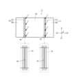
また、図2に示すように、抵抗器1の実装面側(実装面のみならず、抵抗器1のY方向に対向する側面であって実装面に近傍の領域を含む)の接合部13上、及び接合部14上には酸化膜5(5a,5b,5c,5d)が形成されている。これについては図3乃至図6を参照して後述する。 Further, as shown in FIG. 2, on the bonding part 13 on the mounting surface side of the resistor 1 (including not only the mounting surface but also the side surface of the resistor 1 facing in the Y direction and near the mounting surface). , and an oxide film 5 (5a, 5b, 5c, 5d) is formed on the bonding portion 14. This will be described later with reference to FIGS. 3 to 6.

<酸化膜5>
図3は、本実施形態の抵抗器1に形成された酸化膜5(5a)を示す図である。図4は、本実施形態の抵抗器1に形成された酸化膜5(5b)の第1変形例を示す図である。図5は、本実施形態の抵抗器1に形成された酸化膜5(5c)の第2変形例を示す図である。図6は、本実施形態の抵抗器1に形成された酸化膜5(5d)の第3変形例を示す図である。
<Oxide film 5>
FIG. 3 is a diagram showing the oxide film 5 (5a) formed on the resistor 1 of this embodiment. FIG. 4 is a diagram showing a first modification of the oxide film 5 (5b) formed on the resistor 1 of this embodiment. FIG. 5 is a diagram showing a second modification of the oxide film 5 (5c) formed on the resistor 1 of this embodiment. FIG. 6 is a diagram showing a third modification of the oxide film 5 (5d) formed on the resistor 1 of this embodiment.

図3乃至図6に示すように、本実施形態の抵抗器1の実装面側には酸化膜5(5a,5b,5c,5d)が形成されている。酸化膜5(5a,5b,5c,5d)は、抵抗体10、第1電極体11、第2電極体12、のいずれかの実装面側の表面にレーザ照射して加熱することで形成される熱酸化膜である。 As shown in FIGS. 3 to 6, an oxide film 5 (5a, 5b, 5c, 5d) is formed on the mounting surface side of the resistor 1 of this embodiment. The oxide film 5 (5a, 5b, 5c, 5d) is formed by irradiating and heating the mounting surface side of any one of the resistor 10, the first electrode body 11, and the second electrode body 12 with a laser beam. It is a thermal oxide film.

図3では、抵抗器1の実装面側において、抵抗体10と第1電極体11との接合部13から抵抗体10側においてX方向に所定の幅で且つY方向全体に行き渡るように酸化膜5a(5)が形成されている。また図示は省略しているが、抵抗器1の実装面側において、抵抗体10と第2電極体12との接合部14から抵抗体10側においてX方向に所定の幅で且つY方向全体に行き渡るように酸化膜5a(5)が形成されている。 In FIG. 3, on the mounting surface side of the resistor 1, an oxide film is formed from the junction 13 between the resistor 10 and the first electrode body 11 to the resistor 10 side with a predetermined width in the X direction and over the entire Y direction. 5a (5) is formed. Although not shown, on the mounting surface side of the resistor 1, from the joint 14 of the resistor 10 and the second electrode body 12 to the resistor 10 side, a predetermined width in the X direction and the entire Y direction. An oxide film 5a (5) is formed to cover the entire surface.

図4に示す第1変形例では、抵抗器1の実装面側において、抵抗体10と第1電極体11との接合部13から第1電極体11側においてX方向に所定の幅で且つY方向全体に行き渡るように酸化膜5b(5)が形成されている。また図示は省略しているが、抵抗器1の実装面側において、抵抗体10と第2電極体12との接合部14から第2電極体12側においてX方向に所定の幅で且つY方向全体に行き渡るように酸化膜5b(5)が形成されている。 In the first modification shown in FIG. 4, on the mounting surface side of the resistor 1, from the joint 13 between the resistor 10 and the first electrode body 11 to the first electrode body 11 side, a predetermined width in the X direction and Y An oxide film 5b (5) is formed so as to cover the entire direction. Although not shown, on the mounting surface side of the resistor 1, from the joint 14 between the resistor 10 and the second electrode body 12 to the second electrode body 12 side, there is a predetermined width in the X direction and in the Y direction. An oxide film 5b (5) is formed so as to cover the entire surface.

図5に示す第2変形例では、抵抗器1の実装面側において、抵抗体10と第1電極体11との接合部13を覆うようにX方向に所定の幅で且つY方向全体に行き渡るように酸化膜5c(5)が形成されている。また図示は省略しているが、抵抗器1の実装面側において、抵抗体10と第2電極体12との接合部14を覆うようにX方向に所定の幅で且つY方向全体に行き渡るように酸化膜5c(5)が形成されている。 In the second modified example shown in FIG. 5, on the mounting surface side of the resistor 1, it has a predetermined width in the X direction and spreads over the entire Y direction so as to cover the joint 13 between the resistor 10 and the first electrode body 11. An oxide film 5c (5) is formed as shown in FIG. Although not shown in the drawing, on the mounting surface side of the resistor 1, it has a predetermined width in the X direction and extends over the entire Y direction so as to cover the joint 14 between the resistor 10 and the second electrode body 12. An oxide film 5c (5) is formed on.

図6に示す第3変形例における酸化膜5d(5)は、上記の第2変形例の酸化膜5c(5)が抵抗器1の側面(+Y方向に対向する面、及び-Y方向に対向する面)にまで延長したものである。また酸化膜5d(5)は、接合部13、接合部14において全周に亘って形成してもよい。この第3変形例は、図3に示す酸化膜5a(5)、及び図4に示す酸化膜5b(5)にも適用可能である。 The oxide film 5d (5) in the third modification example shown in FIG. It has been extended to the surface of Further, the oxide film 5d(5) may be formed over the entire circumference of the joint portions 13 and 14. This third modification is also applicable to the oxide film 5a (5) shown in FIG. 3 and the oxide film 5b (5) shown in FIG. 4.

このように、酸化膜5(5a,5b,5c,5d)を形成する理由について説明する。 The reason why the oxide film 5 (5a, 5b, 5c, 5d) is formed in this way will be explained.

抵抗器1を回路基板に実装してリフロー工程を行うと、半田が第1電極体11の脚部22、及び第2電極体12の脚部32を伝って、抵抗体10の実装面側にまで這い上がろうとする。しかし、酸化膜5(5a,5b,5c,5d)は、半田に対する濡れ性が低い。よって、抵抗体10と回路基板との間隔が狭く設定されていても半田は酸化膜5(5a,5b,5c,5d)を這い上がりにくくなる。したがって、半田が酸化膜5(5a,5b,5c,5d)を超えて抵抗体10にまで這い上がることを阻止できる。 When the resistor 1 is mounted on a circuit board and a reflow process is performed, the solder flows along the legs 22 of the first electrode body 11 and the legs 32 of the second electrode body 12 and is applied to the mounting surface side of the resistor 10. trying to climb up to However, the oxide film 5 (5a, 5b, 5c, 5d) has low wettability to solder. Therefore, even if the distance between the resistor 10 and the circuit board is set narrow, the solder is difficult to climb up the oxide film 5 (5a, 5b, 5c, 5d). Therefore, it is possible to prevent the solder from creeping up to the resistor 10 beyond the oxide film 5 (5a, 5b, 5c, 5d).

図3のように酸化膜5a(5)を形成することにより、酸化膜5a(5)の脚部22側の縁辺、すなわち第1電極体11の突出部211と接合部13と重なる位置において半田のさらなる這い上がりを阻止できる。また図示は省略するが、酸化膜5a(5)の脚部32側の縁辺、すなわち第2電極体12の突出部311と接合部14と重なる位置で半田のさらなる這い上がりを阻止できる。 By forming the oxide film 5a (5) as shown in FIG. 3, solder is applied to the edge of the oxide film 5a (5) on the leg 22 side, that is, at the position where the protrusion 211 of the first electrode body 11 and the joint 13 overlap. It is possible to prevent the further rise of Further, although not shown, further creeping of the solder can be prevented at the edge of the oxide film 5a (5) on the leg portion 32 side, that is, at the position where the protruding portion 311 of the second electrode body 12 and the joint portion 14 overlap.

図4,5,6のように酸化膜5b,5c,5d(5)を形成することにより、酸化膜5b,5c,5d(5)の脚部22側の縁辺、すなわち第1電極体11の突出部211の脚部22側において-X方向の途中まで移動した位置で半田のさらなる這い上がりを阻止できる。また図示は省略するが、酸化膜5b,5c,5d(5)の脚部32側の縁辺、すなわち脚部32の付け根となる位置から胴体部31において+X方向の途中まで移動した位置で半田のさらなる這い上がりを阻止できる。 By forming the oxide films 5b, 5c, and 5d (5) as shown in FIGS. Further creeping up of the solder can be prevented at a position moved halfway in the −X direction on the leg portion 22 side of the protruding portion 211. Although not shown in the drawings, solder is applied to the edges of the oxide films 5b, 5c, and 5d (5) on the leg 32 side, that is, at a position that is halfway in the +X direction on the body 31 from the base of the leg 32. Further creep can be prevented.

図3に示した酸化膜5a(5)の配置では、半田の這い上がりが、実装面の第1電極体11の抵抗体10との接合位置(接合部13)、実装面の第2電極体12の抵抗体10との接合位置(接合部14)まで及ぶので、第1電極体11及び第2電極体12のTCRの温度変化を、図4乃至図6の酸化膜5b,5c,5d(5)の配置に比べて、より効果的に相殺することができる。 In the arrangement of the oxide film 5a (5) shown in FIG. 12 to the joining position (junction 14) with the resistor 10, the temperature change of the TCR of the first electrode body 11 and the second electrode body 12 can be controlled by the oxide films 5b, 5c, 5d (of FIGS. 4 to 6). This can be offset more effectively than the arrangement 5).

図7は、本実施形態の抵抗器1を半田実装したときの断面写真である。図7に示す抵抗器1は、上記と同様に抵抗体10の端面と第1電極体11の端面を突き合わせ、抵抗体10の端面と第2電極体12の端面とを突き合わせてクラッド接合により形成したものである。ここで、抵抗器1の実装面側において、第2電極体12と抵抗体10との接合部14を跨ぐ境界部位には酸化膜5(図2等参照)を形成しているが、第1電極体11と抵抗体10との接合部13を跨ぐ境界部位には酸化膜5は形成していない。 FIG. 7 is a cross-sectional photograph of the resistor 1 of this embodiment when it is soldered-mounted. The resistor 1 shown in FIG. 7 is formed by clad bonding by abutting the end surfaces of the resistor 10 and the first electrode body 11 and abutting the end surfaces of the resistor 10 and the second electrode body 12 in the same manner as described above. This is what I did. Here, on the mounting surface side of the resistor 1, an oxide film 5 (see FIG. 2, etc.) is formed at a boundary region spanning the joint 14 between the second electrode body 12 and the resistor 10; The oxide film 5 is not formed at the boundary between the electrode body 11 and the resistor 10 across the joint 13.

そして、リフロー工程により抵抗器1を半田9を介して回路基板7に実装した。その結果、右側の第1電極体11の脚部22に接触した半田9は、当該脚部22を這い上がり、実装面において突出部211を経て抵抗体10にまで這い上がり、抵抗体10に接触した状態となっている。一方、第2電極体12の脚部32に接触した半田9は当該脚部32を這い上がり実装面において突出部311にまで這い上がるものの、酸化膜5に接触する位置で這い上がりが阻止されている。したがって、実際の抵抗器1において、第2電極体12と抵抗体10との接合部14を跨ぐ境界部位、及び第1電極体11と抵抗体10との接合部13を跨ぐ境界部位に酸化膜5をそれぞれ形成することにより、半田9の抵抗体10への這い上がりを阻止可能であることが容易に理解できる。 Then, resistor 1 was mounted on circuit board 7 via solder 9 by a reflow process. As a result, the solder 9 that has come into contact with the leg 22 of the first electrode body 11 on the right side crawls up the leg 22, climbs up to the resistor 10 via the protrusion 211 on the mounting surface, and comes into contact with the resistor 10. The situation is as follows. On the other hand, although the solder 9 that has come into contact with the leg 32 of the second electrode body 12 creeps up the leg 32 and reaches the protrusion 311 on the mounting surface, the solder 9 is prevented from creeping up at the position where it contacts the oxide film 5. There is. Therefore, in the actual resistor 1, an oxide film is formed on the boundary region spanning the joint 14 between the second electrode body 12 and the resistor 10, and the boundary region spanning the joint 13 between the first electrode body 11 and the resistor 10. It can be easily understood that by forming the respective resistors 5, it is possible to prevent the solder 9 from creeping up onto the resistor 10.

<トリミング>
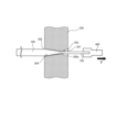
図8は、本実施形態の抵抗器1にトリミングを行う場合の模式図である。図9は、トリミング後の抵抗器1の実装面を示す図である。図10は、トリミング後の抵抗器1の側面図である。
<Trimming>
FIG. 8 is a schematic diagram when trimming the resistor 1 of this embodiment. FIG. 9 is a diagram showing the mounting surface of the resistor 1 after trimming. FIG. 10 is a side view of resistor 1 after trimming.

本実施形態の抵抗器1において、抵抗体10をトリミングすることで抵抗値を調整することができる。トリミングはレーザ光を抵抗体10に照射して抵抗体10の一部を削り取ることにより行われる。また抵抗体10のトリミング箇所には上記の酸化膜5が形成される。よって、トリミング箇所を工夫することで、抵抗値の調整と、半田の這い上がりを阻止する加工とを同時に行うことができる。なお、図3乃至図6に示す酸化膜5を形成する際もレーザ照射を行うが、この場合のレーザ強度はトリミングが発生しない程度に抑制されている。 In the resistor 1 of this embodiment, the resistance value can be adjusted by trimming the resistor 10. Trimming is performed by irradiating the resistor 10 with laser light and scraping off a portion of the resistor 10. Further, the above-mentioned oxide film 5 is formed at the trimming portion of the resistor 10. Therefore, by devising the trimming location, it is possible to adjust the resistance value and perform processing to prevent solder from creeping up at the same time. Note that laser irradiation is also performed when forming the oxide film 5 shown in FIGS. 3 to 6, but the laser intensity in this case is suppressed to such an extent that trimming does not occur.

図8に示すように、抵抗器1の実装面において、接合部13、及び接合部14に対してレーザを照射する。 As shown in FIG. 8, on the mounting surface of the resistor 1, the bonding portions 13 and 14 are irradiated with a laser.

ところで、本実施形態の抵抗器1は、後述のように(図11、図12参照)、抵抗体母材10Aを電極体母材11A,12Aで挟み込んだ状態でクラッド接合(固相接合)した抵抗器母材100をダイス300に挿通して断面積を縮小させつつ断面形状を抵抗器1の断面形状に変形させ、ダイス300に挿通後の抵抗器母材100を切断することで形成される。よって、接合部13(境界部位)及び接合部14(境界部位)は、通常平面(直線)となるが、わずかに蛇行する場合がある。この場合、接合部13及び接合部14のみを狙ってレーザ照射を行うことは困難である。 By the way, in the resistor 1 of this embodiment, as described later (see FIGS. 11 and 12), the resistor base material 10A is sandwiched between the electrode base materials 11A and 12A, and clad bonding (solid phase bonding) is performed. It is formed by inserting the resistor base material 100 through the die 300 to reduce the cross-sectional area and deforming the cross-sectional shape to the cross-sectional shape of the resistor 1, and cutting the resistor base material 100 after being inserted through the die 300. . Therefore, the joint part 13 (boundary part) and the joint part 14 (border part) are usually flat (straight), but may be slightly meandering. In this case, it is difficult to perform laser irradiation targeting only the bonding portions 13 and 14.

そこで、図8の拡大図に示すように、接合部13において抵抗体10及び第1電極体11にレーザが照射され、接合部14において抵抗体10及び第2電極体12にレーザが照射されるようにレーザの照射エリア51(X方向の幅:0.1mm~0.15mm)がそれぞれ設定される。 Therefore, as shown in the enlarged view of FIG. 8, the resistor 10 and the first electrode body 11 are irradiated with the laser at the joint 13, and the resistor 10 and the second electrode 12 are irradiated with the laser at the joint 14. The laser irradiation area 51 (width in the X direction: 0.1 mm to 0.15 mm) is set as follows.

図8の拡大図中の矢印(レーザの照射位置の軌跡)で示すように、レーザは、例えば照射エリア51の-X方向の端部であって平面視で抵抗器1から離間した位置から+Y方向に移動して抵抗器1上を照射して平面視で抵抗器1から離間した位置まで移動する。その後レーザは、+X方向にわずかに移動(移動量はレーザの抵抗器1上のスポット径よりも小さい)して-Y方向に移動して抵抗器1上を照射して平面視で抵抗器1から離間した位置まで移動する。以後同様の動作を繰り返して照射エリア51全体にレーザを照射する。 As shown by the arrow (trajectory of the laser irradiation position) in the enlarged view of FIG. direction, irradiates the resistor 1, and moves to a position separated from the resistor 1 in plan view. After that, the laser moves slightly in the +X direction (the amount of movement is smaller than the spot diameter of the laser spot on resistor 1) and then moves in the -Y direction to irradiate the resistor 1. Move to a position away from. Thereafter, similar operations are repeated to irradiate the entire irradiation area 51 with the laser.

レーザは、その出力が発振直後に過大または過少となるなど安定しない虞があるので、上記のように、平面視で抵抗器1から離間した位置(抵抗器1にレーザが照射されない位置)からレーザの発振を開始して出力が安定したレーザを抵抗器1に照射することが望ましい。また、レーザは照射エリア51の+Y方向(-Y方向)の端部から-Y方向(+Y方向)の端部まで途切れることなく照射することが望ましい。 Since there is a risk that the laser output may be unstable, such as being too high or too low immediately after oscillation, the laser is not irradiated from a position away from resistor 1 in plan view (a position where resistor 1 is not irradiated with the laser), as described above. It is desirable to irradiate the resistor 1 with a laser whose output is stable after starting oscillation. Further, it is desirable that the laser irradiates the irradiation area 51 from the end in the +Y direction (-Y direction) to the end in the -Y direction (+Y direction) without interruption.

また抵抗器1にレーザを照射しているときは、抵抗値が安定しないので、レーザ照射後に抵抗値を測定し、当該抵抗値が所望の抵抗値になるまでレーザ照射と抵抗値の測定を繰り返すことになる。 Also, when the resistor 1 is irradiated with a laser, the resistance value is not stable, so the resistance value is measured after laser irradiation, and the laser irradiation and resistance value measurement are repeated until the resistance value reaches the desired resistance value. It turns out.

上記のように照射エリア51全体にレーザを照射することで、図9、及び図10に示すように、接合部13、及び接合部14に沿って凹部6が形成される。凹部6はY方向に延びるとともにY方向から見た断面形状が略半円形(若しくは矩形、不定形)となる。このように凹部6を形成することで抵抗器1の抵抗値は高抵抗側にシフトする。また上記のように凹部6は照射エリア51の端部から端部まで形成することで、その内壁を中心に熱反応により表面が改質された酸化膜5が形成されるので、リフロー工程の際に半田が抵抗体10にまで這い上がることを阻止できる。よって、一対の酸化膜5間に位置する抵抗体10には、母材の抵抗体10が露出した状態でも、半田が抵抗体10まで這い上がる心配がない。 By irradiating the entire irradiation area 51 with the laser as described above, the recesses 6 are formed along the joints 13 and 14, as shown in FIGS. 9 and 10. The recess 6 extends in the Y direction, and has a substantially semicircular (or rectangular or irregularly shaped) cross-sectional shape when viewed from the Y direction. By forming the recess 6 in this manner, the resistance value of the resistor 1 is shifted to the high resistance side. Furthermore, by forming the recess 6 from end to end of the irradiation area 51 as described above, the oxide film 5 whose surface has been modified by thermal reaction is formed around the inner wall of the recess 6, so that during the reflow process, It is possible to prevent solder from creeping up to the resistor 10. Therefore, there is no fear that the solder will creep up to the resistor 10 located between the pair of oxide films 5 even if the base material resistor 10 is exposed.

<変形例>
図11は、本実施形態の抵抗器1の変形例を示す図である。本実施形態の抵抗器1の変形例は、第1電極体11の脚部22、第2電極体12の脚部32がなく、抵抗器1の実装面が平坦となっている。一方、回路基板7には電極71,72が配置され、電極71,72は、回路基板7から突出するように配置されている。電極71には第1電極体11が半田(不図示)により実装されており、電極72には第2電極体12が半田(不図示)により実装されている。このとき、抵抗体10は、回路基板7から離間して配置されている。
<Modified example>
FIG. 11 is a diagram showing a modification of the resistor 1 of this embodiment. In the modified example of the resistor 1 of this embodiment, the leg portion 22 of the first electrode body 11 and the leg portion 32 of the second electrode body 12 are absent, and the mounting surface of the resistor 1 is flat. On the other hand, electrodes 71 and 72 are arranged on the circuit board 7, and the electrodes 71 and 72 are arranged so as to protrude from the circuit board 7. The first electrode body 11 is mounted on the electrode 71 using solder (not shown), and the second electrode body 12 is mounted on the electrode 72 using solder (not shown). At this time, the resistor 10 is placed apart from the circuit board 7.

上記と同様に抵抗器1の実装面において、例えば接合部13,14を覆うように酸化膜5が配置されている。このため、リフロー工程において、第1電極体11を伝ってきた半田が接合部13に形成された酸化膜5を超えて抵抗体10にまで這い上がること、及び第2電極体12を伝ってきた半田が接合部14に形成された酸化膜5を超えて抵抗体10にまで這い上がることを阻止できる。なお、この変形例においても、上記の凹部6(酸化膜5)を形成してもよい。 Similarly to the above, the oxide film 5 is disposed on the mounting surface of the resistor 1 so as to cover, for example, the joints 13 and 14. Therefore, in the reflow process, the solder that has passed through the first electrode body 11 may creep up to the resistor 10 over the oxide film 5 formed on the joint 13, and the solder that has passed through the second electrode body 12 may creep up to the resistor 10. It is possible to prevent solder from creeping up to the resistor 10 over the oxide film 5 formed on the joint portion 14. Note that in this modification as well, the recess 6 (oxide film 5) described above may be formed.

<本実施形態の効果>
次に、本実施形態による作用効果について説明する。
<Effects of this embodiment>
Next, the effects of this embodiment will be explained.

本実施形態の抵抗器1によれば、抵抗体10と、抵抗体10に接続された一対の電極(第1電極体11、第2電極体12)と、を備え、基板(回路基板)に実装した場合に少なくとも抵抗体10が基板(回路基板)から離間して配置される抵抗器1であって、抵抗器1の実装面(実装面側)の抵抗体10と電極(第1電極体11、第2電極体12)との境界部位(接合部13、接合部14)のうち、抵抗体10及び電極(第1電極体11、第2電極体12)の少なくとも一方に酸化膜5を有する。 According to the resistor 1 of the present embodiment, the resistor 10 includes a resistor 10 and a pair of electrodes (first electrode body 11, second electrode body 12) connected to the resistor 10, and is mounted on a substrate (circuit board). A resistor 1 in which at least the resistor 10 is placed apart from a substrate (circuit board) when mounted, the resistor 10 and the electrode (first electrode body) on the mounting surface (mounting surface side) of the resistor 1 11. An oxide film 5 is formed on at least one of the resistor 10 and the electrode (first electrode body 11, second electrode body 12) among the boundary parts (junction 13, junction 14) with the second electrode body 12). have

上記構成により、抵抗体10と抵抗体10に接続された一対の電極(第1電極体11、第2電極体12)に構成されるので小型且つ低抵抗な抵抗器1が実現できる。また、酸化膜5は半田に対する濡れ性が低い。よって、抵抗体10と基板(回路基板)との間隔が狭くなっても半田が酸化膜5によって這い上がりにくくなるので、半田が酸化膜5を超えて抵抗体10まで這い上がることを阻止できる。したがって、抵抗体10を樹脂で覆う場合に比べて、製造歩留まりを高め、且つ製造コストを抑制することができる。 With the above configuration, it is possible to realize a small and low-resistance resistor 1 since it is configured with the resistor 10 and a pair of electrodes (first electrode body 11, second electrode body 12) connected to the resistor 10. Further, the oxide film 5 has low wettability to solder. Therefore, even if the distance between the resistor 10 and the substrate (circuit board) becomes narrow, the solder is difficult to creep up due to the oxide film 5, so that the solder can be prevented from creeping up beyond the oxide film 5 to the resistor 10. Therefore, compared to the case where the resistor 10 is covered with resin, manufacturing yield can be increased and manufacturing costs can be suppressed.

本実施形態において、酸化膜5は、少なくとも抵抗体10に形成されている(図3、図5参照)。これにより、半田の這い上がりが電極(第1電極体11、第2電極体12)と抵抗体10との接合位置(接合部13、接合部14)まで及ぶので、電極(第1電極体11、第2電極体12)のTCRの温度変化を、効果的に相殺することができる。 In this embodiment, the oxide film 5 is formed at least on the resistor 10 (see FIGS. 3 and 5). As a result, the solder creeps up to the joint positions (joint parts 13, 14) between the electrodes (first electrode body 11, second electrode body 12) and the resistor 10, so that , the temperature change in the TCR of the second electrode body 12) can be effectively offset.

本実施形態において、抵抗体10の表面は、酸化膜5が形成された部位を除き母材の抵抗体が露出している。すなわち、酸化膜5が電極(第1電極体11、第2電極体12)に形成されている場合(図4など)において、抵抗体10の表面は母材の抵抗体である金属材が露出している。これにより、抵抗体10の表面、特には抵抗体10の実装面、さらには例えば抵抗体10の側面の実装面側を樹脂で覆うことなく抵抗体10への半田の這い上がりを阻止できる。 In this embodiment, on the surface of the resistor 10, the base material resistor is exposed except for the portion where the oxide film 5 is formed. That is, when the oxide film 5 is formed on the electrodes (first electrode body 11, second electrode body 12) (as shown in FIG. 4, etc.), the surface of the resistor 10 is such that the metal material that is the base material resistor is exposed. are doing. Thereby, it is possible to prevent solder from creeping up onto the resistor 10 without covering the surface of the resistor 10, particularly the mounting surface of the resistor 10, and further, for example, the mounting surface side of the side surface of the resistor 10 with resin.

本実施形態において、電極(第1電極体11、第2電極体12)は、抵抗体10に接続する胴体部21,31と、基板(回路基板)の方向に突出した脚部22,32と、を有するとともに抵抗体10と胴体部21,31(突出部211、311)により境界部位(接合部13、接合部14)が形成され、酸化膜5は、抵抗体10と胴体部21,31(突出部211、311)との境界部位(接合部13、接合部14)のうち、少なくとも胴体部21,31(図4参照)に形成されている。これにより、脚部22,32と半田との接合を確保しつつ抵抗体10への半田の這い上がりを阻止できる。 In this embodiment, the electrodes (first electrode body 11, second electrode body 12) have body parts 21 and 31 connected to the resistor 10, and leg parts 22 and 32 that protrude toward the board (circuit board). , and a boundary region (junction 13, junction 14) is formed between the resistor 10 and the body parts 21, 31 (projections 211, 311), and the oxide film 5 is formed between the resistor 10 and the body parts 21, 31. (Protrusion parts 211, 311) Among the boundary parts (joint part 13, joint part 14), it is formed at least in body parts 21, 31 (see FIG. 4). This makes it possible to prevent the solder from creeping up onto the resistor 10 while ensuring the connection between the legs 22 and 32 and the solder.

本実施形態において、境界部位(接合部13、接合部14)において、凹部6を有し、酸化膜5は凹部6、または凹部6の内壁を中心とする凹部6周辺に形成されている。これにより、抵抗値の調整と、半田の這い上がりを阻止する加工とを同時に行うことができる。 In this embodiment, a recess 6 is provided at the boundary site (joint part 13, joint part 14), and the oxide film 5 is formed in the recess 6 or around the recess 6 centering on the inner wall of the recess 6. This allows adjustment of the resistance value and processing to prevent solder from creeping up at the same time.

本実施形態において、境界部位(接合部13、接合部14)において、凹部6を有し、酸化膜5は凹部6、又は凹部6の内壁を中心とする凹部6周辺に形成され、凹部6は、胴体部21,31(突出部211、311)と抵抗体10の双方に亘って形成されている。これにより、抵抗値の調整と、半田の這い上がりを阻止する加工とを同時に且つ安定的に行うことができる。 In this embodiment, a recess 6 is provided at the boundary site (junction 13, joint 14), and the oxide film 5 is formed in the recess 6 or around the recess 6 centered on the inner wall of the recess 6. , are formed over both the body parts 21 and 31 (protrusions 211 and 311) and the resistor 10. Thereby, adjustment of the resistance value and processing for preventing solder from creeping up can be performed simultaneously and stably.

本実施形態の抵抗器1の製造方法は、抵抗体10と、抵抗体10に接続された一対の電極(第1電極体11、第2電極体12)と、を備え、基板(回路基板)に実装した時に少なくとも抵抗体10が基板(回路基板)から離間して配置される抵抗器1の製造方法であって、抵抗器1の実装面側の抵抗体10と電極(第1電極体11、第2電極体12)との境界部位(接合部13、接合部14)にレーザを照射することで、抵抗体10及び電極(第1電極体11、第2電極体12)の少なくとも一方に酸化膜5を形成する。 The method for manufacturing the resistor 1 of this embodiment includes a resistor 10 and a pair of electrodes (first electrode body 11, second electrode body 12) connected to the resistor 10, and a substrate (circuit board). A method for manufacturing a resistor 1 in which at least the resistor 10 is placed apart from a substrate (circuit board) when mounted on the resistor 1, the resistor 10 and the electrode (first electrode body 11 , second electrode body 12) by irradiating the laser to the boundary region (joint part 13, joint part 14) to at least one of the resistor 10 and the electrodes (first electrode body 11, second electrode body 12). An oxide film 5 is formed.

上記方法により、抵抗体10と抵抗体10に接続された一対の電極(第1電極体11、第2電極体12)に構成されるので小型且つ低抵抗な抵抗器1が実現できる。また、酸化膜5は半田に対する濡れ性が低い。よって、抵抗体10と基板(回路基板)との間隔が狭くなっても半田が酸化膜5に這い上がりにくくなるので、半田が酸化膜5を超えて抵抗体10まで這い上がることを阻止できる。したがって、抵抗体10を樹脂で覆う場合に比べて、製造歩留まりを高め、且つ製造コストを抑制することができる。 By the above method, it is possible to realize a resistor 1 that is small and has low resistance because it is configured with the resistor 10 and a pair of electrodes (first electrode body 11, second electrode body 12) connected to the resistor 10. Further, the oxide film 5 has low wettability to solder. Therefore, even if the distance between the resistor 10 and the substrate (circuit board) becomes narrower, the solder is less likely to creep up onto the oxide film 5, and the solder can be prevented from creeping up beyond the oxide film 5 to the resistor 10. Therefore, compared to the case where the resistor 10 is covered with resin, manufacturing yield can be increased and manufacturing costs can be suppressed.

その他、本実施形態の抵抗器1は、以下のような構成・作用・効果を有する。 In addition, the resistor 1 of this embodiment has the following configuration, function, and effect.

本実施形態の抵抗器1によれば、抵抗体10と、抵抗体10に接続された一対の電極(第1電極体11、第2電極体12)と、を備えた抵抗器1であって、抵抗体10の端面と、電極の端面(第1電極体11、第2電極体12)とが、突き合わせて接合され、電極(第1電極体11、第2電極体12)は、胴体部21,31と胴体部21,31から実装面に突出した脚部22,32と、を含み、抵抗器1の長辺の長さ寸法(L)は、3.2mm以下であり、抵抗値は2mΩ以下である。 According to the resistor 1 of the present embodiment, the resistor 1 includes a resistor 10 and a pair of electrodes (first electrode body 11, second electrode body 12) connected to the resistor 10. , the end face of the resistor 10 and the end face of the electrode (first electrode body 11, second electrode body 12) are butted and joined, and the electrode (first electrode body 11, second electrode body 12) is connected to the body part. 21, 31 and legs 22, 32 protruding from the body parts 21, 31 to the mounting surface, the length dimension (L) of the long side of the resistor 1 is 3.2 mm or less, and the resistance value is It is 2 mΩ or less.

上記構成により、抵抗体10と抵抗体10に接続された一対の電極(第1電極体11、第2電極体12)により胴体部21,31から実装面に突出した脚部22,32が構成され、検出端子からの引き出しが脚部22,32間で行えるため、小型の抵抗器1が実現できる。また、抵抗体10の両端に電極(第1電極体11、第2電極体12)が接合された形態であり、抵抗体10の(X方向の)寸法は抵抗器1の(X方向の)寸法よりも小さくなるので、抵抗体10の下面に一対の電極を接合したタイプの抵抗器よりも低抵抗な抵抗器1を実現できる。以上より、小型化(長辺寸法3.2mm以下、3216サイズ以下)を実現しつつ従来にはないさらなる低抵抗(2mΩ以下)を実現可能な抵抗器1となる。 With the above configuration, the leg portions 22, 32 protruding from the body portions 21, 31 to the mounting surface are configured by the resistor 10 and a pair of electrodes (first electrode body 11, second electrode body 12) connected to the resistor 10. Since the detection terminal can be drawn out between the legs 22 and 32, a small resistor 1 can be realized. Further, electrodes (first electrode body 11, second electrode body 12) are connected to both ends of the resistor 10, and the dimensions (in the X direction) of the resistor 10 are the same as those of the resistor 1 (in the X direction). Since the size of the resistor 1 is smaller than that of the resistor 10, it is possible to realize a resistor 1 having a lower resistance than a resistor of a type in which a pair of electrodes are bonded to the lower surface of the resistor 10. As described above, the resistor 1 can realize a lower resistance than ever before (2 mΩ or less) while realizing miniaturization (long side dimension 3.2 mm or less, 3216 size or less).

なお、抵抗体と電極体とを電子ビームなどにより溶接して形成された抵抗器であれば、このサイズでは抵抗値に当該溶接によるビードの影響を考慮する必要があるが、本実施形態の抵抗器1は、後述のように、抵抗体10と第1電極体11、及び抵抗体10と第2電極体12とがそれぞれ拡散接合により接合可能であるため、このように小型に設計しても抵抗値等の特性を安定させることができる。 Note that if the resistor is formed by welding the resistor and electrode body using an electron beam or the like, it is necessary to take into account the effect of the bead caused by the welding on the resistance value for this size, but the resistor of this embodiment As described later, the resistor 10 and the first electrode body 11 and the resistor 10 and the second electrode body 12 can be joined by diffusion bonding, so even if the device 1 is designed to be small in size, Characteristics such as resistance value can be stabilized.

本実施形態において、抵抗器1の実装面のうち、抵抗体10と胴体部21,31との境界部位(接合部13,14)は平坦である。電子ビームなどの溶接による溶接ビードを有していないことにより、抵抗体10と胴体部21,31との境界が明確になり、良否判断を容易に行うことができる。また、抵抗器1をシャント抵抗器として用いた場合、抵抗体10と胴体部21,31との境界(接合部13,14)で段差が生じることにより発生する電流の検出精度の低下を抑制できる。更に、抵抗値、熱特性の安定性を向上させることができる。 In this embodiment, among the mounting surfaces of the resistor 1, the boundary parts (joint parts 13, 14) between the resistor 10 and the body parts 21, 31 are flat. Since there is no weld bead formed by welding with an electron beam or the like, the boundary between the resistor 10 and the body portions 21 and 31 becomes clear, making it easy to judge whether the resistor is good or bad. Furthermore, when the resistor 1 is used as a shunt resistor, it is possible to suppress a decrease in current detection accuracy caused by a step at the boundary between the resistor 10 and the body parts 21 and 31 (joint parts 13 and 14). . Furthermore, resistance value and stability of thermal characteristics can be improved.

本実施形態において、抵抗体10と胴体部21,31とは固相接合により接合されている。これにより、抵抗体10と第1電極体11、及び抵抗体10と第2電極体12とが互いに強固に接合されるため、良好な電気的特性が得られる。また、抵抗器1では、抵抗体10と第1電極体11、及び抵抗体10と第2電極体12との接合には電子ビームなどによる溶接が用いられていないため、接合部13,14には溶接ビード(凹凸形状の溶接痕)がない。したがって、抵抗器1の表面にワイヤーボンディング等を施す場合にボンディング性を損なうことがない。 In this embodiment, the resistor 10 and the body portions 21, 31 are joined by solid phase joining. Thereby, the resistor 10 and the first electrode body 11 and the resistor 10 and the second electrode body 12 are firmly joined to each other, so that good electrical characteristics can be obtained. In addition, in the resistor 1, welding using an electron beam or the like is not used to join the resistor 10 and the first electrode body 11, and the resistor 10 and the second electrode body 12, so that the joints 13 and 14 are There are no weld beads (uneven weld marks). Therefore, when wire bonding or the like is performed on the surface of the resistor 1, the bonding performance is not impaired.

本実施形態において、胴体部21,31は、抵抗体側に突出した突出部211,311を有する。これにより、抵抗器1の長手方向(X方向)の長さ(L)を一定としたとき、突出部211のX方向の長さ(胴体部21の長さL1)、又は突出部311のX方向の長さ(胴体部31のX方向の長さL2)を任意に調整し、抵抗体10のX方向の長さ(L0)をL0=L-(L1+L2)として調整することができる。したがって、脚部22,32の形状を変更することなく、抵抗器1の抵抗値を任意に調整することができる。 In this embodiment, the body parts 21 and 31 have protrusions 211 and 311 that protrude toward the resistor side. As a result, when the length (L) of the resistor 1 in the longitudinal direction (X direction) is constant, the length of the protrusion 211 in the X direction (length L1 of the body part 21) or the length of the protrusion 311 in the The length in the X direction (the length L2 of the body portion 31 in the X direction) can be arbitrarily adjusted, and the length (L0) of the resistor 10 in the X direction can be adjusted as L0=L−(L1+L2). Therefore, the resistance value of the resistor 1 can be adjusted arbitrarily without changing the shape of the legs 22, 32.

本実施形態において、抵抗器1の抵抗体10及び電極(第1電極体11、第2電極体12)の並び方向(X方向)における脚部22,32の実装面側の端部は、面取り形状となっている。 In this embodiment, the ends of the legs 22 and 32 on the mounting surface side in the direction in which the resistor 10 and electrodes (first electrode body 11, second electrode body 12) of the resistor 1 are arranged (X direction) are chamfered. It has a shape.

従来の抵抗器では、面取りされていない角部分において電流密度が大となり、エレクトロマイグレーションと呼ばれる現象が発生したり、同様にして角部分に熱応力が集中したりすることにより、抵抗器の欠損が発生しやすくなっていた。また、このエレクトロマイグレーションは、回路サイズが微小化するにつれて無視できない影響を及ぼすため、抵抗器が小型になるほど、エレクトロマイグレーションが顕著化することが懸念されていた。 In conventional resistors, the current density is high at the corners that are not chamfered, causing a phenomenon called electromigration, and thermal stress is similarly concentrated at the corners, resulting in resistor failure. It was becoming more likely to occur. In addition, this electromigration has a non-negligible effect as the circuit size becomes smaller, so there has been a concern that the smaller the resistor, the more prominent the electromigration becomes.

これに対して、抵抗器1は、角部分Pが面取りされていることにより、角部分Pにおける電流密度の偏りが緩和される。これにより、エレクトロマイグレーションの発生を抑制することができる。また、同様にして、熱応力集中が緩和できるため、ヒートサイクル耐性を向上することができる。 On the other hand, since the corner portions P of the resistor 1 are chamfered, the bias in current density at the corner portions P is alleviated. Thereby, the occurrence of electromigration can be suppressed. Further, in the same way, thermal stress concentration can be alleviated, so that heat cycle resistance can be improved.

本実施形態において、抵抗器1の抵抗体10及び電極(第1電極体11、第2電極体12)の並び方向(X方向)及び抵抗器1の実装方向に垂直な方向(Z方向)を幅方向(Y方向)とし、抵抗体10の表面、及び/又は、電極(第1電極体11、第2電極体12)の表面には幅方向(Y方向)に沿って延びる筋状の凹凸面(筋状凹凸15)が形成されている。これにより、抵抗器1の表面積を大きくして放熱性を高めることができ、また電極(第1電極体11、第2電極体12)に形成した場合は抵抗器1を回路基板に固定する半田の接合強度を高めることができる。 In this embodiment, the direction in which the resistor 10 and electrodes (first electrode body 11, second electrode body 12) of the resistor 1 are arranged (X direction) and the direction perpendicular to the mounting direction of the resistor 1 (Z direction) are In the width direction (Y direction), the surface of the resistor 10 and/or the surface of the electrodes (first electrode body 11, second electrode body 12) has streak-like unevenness extending along the width direction (Y direction). A surface (stripe unevenness 15) is formed. As a result, the surface area of the resistor 1 can be increased to improve heat dissipation, and when formed on the electrodes (first electrode body 11, second electrode body 12), the solder that fixes the resistor 1 to the circuit board can be used. It is possible to increase the bonding strength of

本実施形態において、抵抗体10は、直方体(又は立方体)に形成されている。抵抗体10が直方体(又は立方体)であると、抵抗体10の端面と略同形状に形成され、抵抗体10の端面に接合された第1電極体11及び第2電極体12から抵抗体10を流れる電流の経路が直線的になるため抵抗値を安定にすることができる。また、抵抗器1では、抵抗体10が第1電極体11と第2電極体12の間に接合されているため、抵抗体10の体積を必要最小限にして抵抗値を調整することが可能である。 In this embodiment, the resistor 10 is formed into a rectangular parallelepiped (or cube). When the resistor 10 is a rectangular parallelepiped (or cube), the resistor 10 is formed in substantially the same shape as the end surface of the resistor 10, and the resistor 10 is The resistance value can be stabilized because the path of current flowing through it becomes linear. In addition, in the resistor 1, since the resistor 10 is joined between the first electrode body 11 and the second electrode body 12, it is possible to adjust the resistance value by minimizing the volume of the resistor 10. It is.

[抵抗器の製造方法の説明]
図12は、本実施形態の抵抗器1の製造方法を説明する模式図である。
[Explanation of resistor manufacturing method]
FIG. 12 is a schematic diagram illustrating a method for manufacturing the resistor 1 of this embodiment.

本実施形態の抵抗器1の製造方法は、材料を準備する工程(a)と、材料を接合する工程(b)と、形状を加工する工程(c)と、個々の抵抗器1に切断(個片化)する工程(d)と、レーザを用いて抵抗器1の抵抗値を調整する工程(e)とを備える。 The method for manufacturing the resistor 1 of this embodiment includes a step (a) of preparing materials, a step (b) of joining the materials, a step (c) of processing the shape, and a step (c) of cutting the resistors 1 into individual resistors 1. the step (d) of dividing the resistor 1 into individual pieces) and the step (e) of adjusting the resistance value of the resistor 1 using a laser.

材料を準備する工程(a)では、抵抗体10の母材となる抵抗体母材10Aと、第1電極体11の母材である電極体母材11Aと、第2電極体12の母材である電極体母材11A,12Aを準備する。抵抗体母材10Aと、電極体母材11A,12Aは平角状の長尺の線材である。本実施形態では、抵抗器1のサイズ、抵抗値及び加工性の観点から、抵抗体母材10A(抵抗体10)の材料として銅・マンガン系合金を使用し、電極体母材11A,12A(第1電極体11、第2電極体12)の材料として無酸素銅(C1020)を使用することが好ましい。 In the step (a) of preparing materials, a resistor base material 10A that is the base material of the resistor 10, an electrode base material 11A that is the base material of the first electrode body 11, and a base material of the second electrode body 12 are prepared. Electrode body base materials 11A and 12A are prepared. The resistor base material 10A and the electrode base materials 11A and 12A are rectangular long wire rods. In this embodiment, from the viewpoint of the size, resistance value, and workability of the resistor 1, a copper-manganese alloy is used as the material of the resistor base material 10A (resistor 10), and the electrode body base materials 11A, 12A ( It is preferable to use oxygen-free copper (C1020) as the material for the first electrode body 11 and the second electrode body 12).

材料を接合する工程(b)では、電極体母材11Aと抵抗体母材10Aと電極体母材12Aとを、この順で重ね、重ね方向に圧力を加えて接合して抵抗器母材100を形成する。 In the step (b) of joining the materials, the electrode body base material 11A, the resistor base material 10A, and the electrode body base material 12A are stacked in this order and joined by applying pressure in the stacking direction to form the resistor base material 100. form.

すなわち、工程(b)では、いわゆる異種金属材料間におけるクラッド接合(固相接合)が行われる。クラッド接合された電極体母材11Aと抵抗体母材10Aとの接合面、及び電極体母材12Aと抵抗体母材10Aとの接合面は、双方の金属原子が互いに拡散した拡散接合面となっている。 That is, in step (b), so-called clad bonding (solid-phase bonding) between dissimilar metal materials is performed. The bonding surface between the clad-bonded electrode body base material 11A and the resistor base material 10A, and the bonding surface between the electrode body base material 12A and the resistor base material 10A are diffusion bonded surfaces in which metal atoms of both materials are diffused into each other. It has become.

これにより、従来のような電子ビームによる溶接等を行うことなく、抵抗体母材10Aと電極体母材11Aとの接合面、及び抵抗体母材10Aと電極体母材12Aとの接合面を互いに強固に接合することができる。また、抵抗体母材10A(抵抗体10)と電極体母材11A(第1電極体11)との接合面及び抵抗体母材10A(抵抗体10)と電極体母材12A(第2電極体12)との接合面において、良好な電気的特性が得られる。 As a result, the bonding surface between the resistor base material 10A and the electrode body base material 11A, and the joint surface between the resistor base material 10A and the electrode body base material 12A can be bonded without performing welding using an electron beam as in conventional methods. They can be firmly bonded to each other. Also, the bonding surface between the resistor base material 10A (resistor 10) and the electrode base material 11A (first electrode body 11), and the joint surface between the resistor base material 10A (resistor 10) and the electrode body base material 12A (second electrode Good electrical characteristics can be obtained at the interface with the body 12).

図13は、図12に示す工程(c)に用いられるダイス300を引き抜き方向Fの上流側から見た正面図である。図14は、図13のB-B線断面図であって、本実施形態の抵抗器1の製造方法における形状を加工する工程を説明する模式図である。工程(c)では、クラッド接合によって得られた抵抗器母材100をダイス300に通過させる。本実施形態の抵抗器1を製造するにあたっては、一例として、図13に示すダイス300を用いることができる。 FIG. 13 is a front view of the die 300 used in step (c) shown in FIG. 12, viewed from the upstream side in the drawing direction F. FIG. 14 is a cross-sectional view taken along the line BB in FIG. 13, and is a schematic diagram illustrating a step of processing the shape in the method for manufacturing the resistor 1 of this embodiment. In step (c), the resistor base material 100 obtained by clad bonding is passed through a die 300. In manufacturing the resistor 1 of this embodiment, a die 300 shown in FIG. 13 can be used as an example.

ダイス300には、開口部301が形成されている。開口部301は、抵抗器母材100が挿入可能な寸法に設定された入口開口302と、抵抗器母材100の外形寸法よりも小さい寸法に設定された出口開口303と、入口開口302から出口開口303に向けてテーパ状に形成された挿通部304とを有する。本実施形態においては、開口部301は、角部分が面取り形状に加工された矩形に形成されている。 An opening 301 is formed in the die 300. The opening 301 includes an inlet opening 302 set to a size that allows the resistor base material 100 to be inserted, an outlet opening 303 set to a size smaller than the external dimensions of the resistor base material 100, and an exit from the inlet opening 302. The insertion portion 304 is tapered toward the opening 303. In this embodiment, the opening 301 is formed in a rectangular shape with chamfered corners.

このような形状のダイス300に抵抗器母材100を通過させることにより、抵抗器母材100を全方向から圧縮変形させることができる。これにより抵抗器母材100の断面形状はダイス300(出口開口303)の外形に倣った形状となる。 By passing the resistor base material 100 through the die 300 having such a shape, the resistor base material 100 can be compressively deformed from all directions. As a result, the cross-sectional shape of the resistor base material 100 follows the outer shape of the die 300 (exit opening 303).

また、本実施形態では、工程(c)において、抵抗器母材100をダイス300に通過させる際、抵抗器母材100をつかみ具400によって引き抜く、引き抜き工法が適用される。 Furthermore, in the present embodiment, a drawing method is applied in which the resistor base material 100 is pulled out using the grip 400 when the resistor base material 100 is passed through the die 300 in step (c).

工程(c)では、開口部301のサイズを異ならせた複数のダイス300を用意して、これら複数のダイス300を段階的に通過させる引き抜き加工を施してもよい。 In step (c), a plurality of dies 300 having openings 301 of different sizes may be prepared, and a drawing process may be performed in which the dies 300 are passed through the plurality of dies 300 in stages.

また、工程(c)では、ダイス300の開口部301の形状を変更することにより、本実施形態の抵抗器1を製造することができる。 Furthermore, in step (c), the resistor 1 of this embodiment can be manufactured by changing the shape of the opening 301 of the die 300.

抵抗器1を製造するにあたっては、一例として、開口部301(入口開口302、出口開口303)の一の辺における一部に、開口中央に向けて矩形に突出した形状の突出部300aを有するダイス300を適用する。抵抗器母材100には、矩形形状の出口開口303に設けられた突出形状により、引き抜き方向に連続する矩形溝105が形成される。 In manufacturing the resistor 1, for example, a die is used which has a protrusion 300a in a rectangular shape protruding toward the center of the opening on a part of one side of the opening 301 (inlet opening 302, outlet opening 303). Apply 300. A rectangular groove 105 that is continuous in the drawing direction is formed in the resistor base material 100 by a protruding shape provided in the rectangular outlet opening 303 .

抵抗器母材100を個々に切断した際に、この矩形溝105は、抵抗体10と第1電極体11の胴体部21と脚部22、第2電極体12の胴体部31と脚部32によって囲まれる凹部を構成する。 When the resistor base material 100 is individually cut, the rectangular grooves 105 are formed in the body part 21 and the leg part 22 of the resistor 10 and the first electrode body 11, and in the body part 31 and the leg part 32 of the second electrode body 12. constitutes a recess surrounded by.

図12に戻り、工程(c)に続く工程(d)では、設計されたY方向の長さWになるように、抵抗器母材100から抵抗器1を切り出す。また、本実施形態では、工程(d)において、抵抗器母材100において矩形溝105が形成された面100aから反対面100bに向けて切断することが好ましい。これにより、金属のバリ(Burr)は抵抗器1の上面から上方に向けて延びる形に形成され、脚部22,32において-Z方向(図1、図2)に延びるバリ(回路基板に向けて延びるバリ)が発生することはない。これにより、抵抗器1の回路基板への実装を確実に行うことができる。 Returning to FIG. 12, in step (d) following step (c), resistor 1 is cut out from resistor base material 100 to have the designed length W in the Y direction. Further, in the present embodiment, in step (d), it is preferable that the resistor base material 100 is cut from the surface 100a where the rectangular groove 105 is formed toward the opposite surface 100b. As a result, a metal burr is formed extending upward from the top surface of the resistor 1, and a burr extending in the -Z direction (FIGS. 1 and 2) on the legs 22 and 32 is formed toward the circuit board. No burrs (extending burrs) will occur. Thereby, the resistor 1 can be reliably mounted on the circuit board.

以上の工程を経ることにより、抵抗器母材100から個片の抵抗器1を得ることができる。更に、工程(e)では、レーザ照射により抵抗体10のトリミングを行って抵抗器1の抵抗値を所望の抵抗値に設定する。トリミングの詳細については上記の通りである(図8乃至図10参照)。なお、図1、2に示す、角部分Pはダイス300の開口部301の形状に倣って形成され、筋状凹凸15は抵抗器母材100がダイス300の内壁(出口開口303)に圧接した状態で摺動するときに抵抗器母材100の長さ方向に形成される筋状の摺動痕である。 By going through the above steps, individual pieces of resistor 1 can be obtained from resistor base material 100. Further, in step (e), the resistor 10 is trimmed by laser irradiation to set the resistance value of the resistor 1 to a desired resistance value. The details of trimming are as described above (see FIGS. 8 to 10). Note that the corner portion P shown in FIGS. 1 and 2 is formed following the shape of the opening 301 of the die 300, and the striped unevenness 15 is formed when the resistor base material 100 is pressed against the inner wall (exit opening 303) of the die 300. This is a streak-like sliding trace formed in the length direction of the resistor base material 100 when the resistor base material 100 is slid in the state.

<本実施形態のダイス300を用いた抵抗器1の製造方法の効果>
次に、本実施形態の作用効果について説明する。
<Effects of the method for manufacturing the resistor 1 using the dice 300 of this embodiment>
Next, the effects of this embodiment will be explained.

本実施形態のダイス300を用いた抵抗器1の製造方法によれば、電極体母材11Aと抵抗体母材10Aと電極体母材12Aとを並列に重ねて圧力を加えて、クラッド接合(固相接合)により一体化した構造(すなわち並接クラッド構造)の抵抗器母材100(抵抗器1)が得られる。これにより、電子ビームによる溶接等を用いること無く、抵抗体母材10A(抵抗体10)と電極体母材11A(第1電極体11)の接合強度、及び抵抗体母材10A(抵抗体10)と電極体母材12A(第2電極体12)の接合強度を高めることができる。 According to the method for manufacturing the resistor 1 using the dice 300 of this embodiment, the electrode body base material 11A, the resistor base material 10A, and the electrode body base material 12A are stacked in parallel and pressure is applied to clad bond ( A resistor base material 100 (resistor 1) having an integrated structure (that is, a parallel clad structure) is obtained by solid phase bonding. As a result, the bonding strength between the resistor base material 10A (resistor 10) and the electrode base material 11A (first electrode body 11) and the resistor base material 10A (resistor 10) can be improved without using electron beam welding or the like. ) and the electrode body base material 12A (second electrode body 12) can be increased in bonding strength.

また、本実施形態の上記製造方法によれば、抵抗器母材100をダイス300に通して全方向から圧縮することにより、抵抗器母材100の外形状を成型することができる。このため、抵抗器母材100が形成された後は、工程(d)を経るだけで個別の抵抗器1を製造できる。したがって、抵抗器1の製造によって生じる個体差を抑えることができる。また、これに加えて、抵抗器母材100をダイス300に通すことにより、抵抗体10と第1電極体11との接合強度、及び抵抗体10と第2電極体12との接合強度を更に高めることができる。 Further, according to the manufacturing method of the present embodiment, the outer shape of the resistor base material 100 can be molded by passing the resistor base material 100 through the die 300 and compressing it from all directions. Therefore, after the resistor base material 100 is formed, individual resistors 1 can be manufactured by simply going through step (d). Therefore, individual differences caused by manufacturing the resistor 1 can be suppressed. In addition, by passing the resistor base material 100 through the die 300, the bond strength between the resistor 10 and the first electrode body 11 and the bond strength between the resistor 10 and the second electrode body 12 are further increased. can be increased.

抵抗器母材100を全方向から圧縮する方法としては、例えば、抵抗器母材100が方形であれば、抵抗器母材100を厚み方向(Z)から加圧する一対のローラによって第1段の圧接を施して、その後、幅方向(Y)から加圧する一対のローラによって第2段の圧接を施す方法がある。 As a method for compressing the resistor base material 100 from all directions, for example, if the resistor base material 100 is square, the resistor base material 100 is compressed in the first stage by a pair of rollers that press the resistor base material 100 from the thickness direction (Z). There is a method in which pressure is applied and then a second stage of pressure is applied using a pair of rollers that apply pressure from the width direction (Y).

しかし、この方法では、第1段の圧接工程において、抵抗器母材100は、厚み方向(Z)に圧縮されるものの、幅方向(Y)には膨張してしまう。また、続く第2段の圧接工程において、抵抗器母材100は、幅方向(Y)に圧縮されるものの、厚み方向(Z)には膨張してしまう。この結果、寸法精度が低下し、個々の抵抗器のばらつきや抵抗器への電力印加時の温度分布のばらつき等が大きくなってしまう。 However, in this method, although the resistor base material 100 is compressed in the thickness direction (Z) in the first stage pressure welding step, it expands in the width direction (Y). Further, in the subsequent second stage pressure welding process, the resistor base material 100 is compressed in the width direction (Y), but expands in the thickness direction (Z). As a result, dimensional accuracy decreases, and variations in individual resistors, variations in temperature distribution when power is applied to the resistors, etc. increase.

これに対して、本実施形態の上記製造方法によれば、抵抗器母材100をダイス300に通過させる引き抜き工程を行うことにより、抵抗器母材100を長さ方向(X)及び厚み方向(Z)に一様に圧縮できる。 On the other hand, according to the manufacturing method of the present embodiment, the resistor base material 100 is drawn in the length direction (X) and the thickness direction ( Z) can be uniformly compressed.

このため、ローラを用いて一方向からの圧縮と他方向からの圧縮とを繰り返すことで得られた抵抗器母材に比べて、抵抗器母材100は、電気的に有利な接合界面が形成されると考えられる。したがって、完成品としての抵抗器1の特性差を抑えることができる。 Therefore, compared to a resistor base material obtained by repeating compression from one direction and compression from the other direction using a roller, the resistor base material 100 forms an electrically advantageous bonding interface. It is thought that it will be done. Therefore, differences in characteristics of the resistor 1 as a finished product can be suppressed.

本実施形態の上記製造方法では、特に、開口部301の異なる複数のダイス300を段階的に用いて、抵抗器母材100のサイズを段階的に小さくなるように圧縮成型することにより、抵抗器母材100やダイス300への負荷を低減しつつ、抵抗器母材100を長さ方向(X)及び厚み方向(Z)に一様に圧縮できる。これにより、完成品としての抵抗器1の特性のバラツキを抑えることができる。 In the above manufacturing method of the present embodiment, in particular, a plurality of dies 300 having different openings 301 are used in stages to compress and mold the resistor base material 100 so that the size of the resistor base material 100 is gradually reduced. The resistor base material 100 can be compressed uniformly in the length direction (X) and thickness direction (Z) while reducing the load on the base material 100 and the die 300. Thereby, variations in the characteristics of the resistor 1 as a finished product can be suppressed.

また、本実施形態の上記製造方法では、抵抗器母材100をダイス300に通す工程(c)において、引き抜き工程が適用されることにより、押し出し工法に比べて完成品の精度が高められる。この製造方法を用いることにより、抵抗器1としての特性の安定化を実現できる。 Further, in the above manufacturing method of the present embodiment, in the step (c) of passing the resistor base material 100 through the die 300, a drawing step is applied, so that the accuracy of the finished product is improved compared to the extrusion method. By using this manufacturing method, the characteristics of the resistor 1 can be stabilized.

特に、ダイス300の開口部301の、少なくとも出口開口303は曲線により連続して形成されている。これにより、抵抗器母材100が開口を通過する際に抵抗器母材100に印加される応力を緩和することができ、抵抗器母材100やダイス300への負荷を低減することができる。これにより、完成品としての抵抗器1の特性のバラツキを抑えることができる。 In particular, at least the exit opening 303 of the opening 301 of the die 300 is continuously formed in a curved line. Thereby, the stress applied to the resistor base material 100 when the resistor base material 100 passes through the opening can be relaxed, and the load on the resistor base material 100 and the dice 300 can be reduced. Thereby, variations in the characteristics of the resistor 1 as a finished product can be suppressed.

これに加え、少なくとも出口開口303は曲線により連続して形成されているので、ダイス300を通過して得られた抵抗器1の角部分P(縁辺)は面取りされることになる。これにより、角部分Pにおいて抵抗器1に生じるエレクトロマイグレーションを抑制することができる。また、抵抗器1のヒートサイクル耐性を高めることができる。 In addition, since at least the outlet opening 303 is formed continuously in a curved line, the corner portion P (edge) of the resistor 1 obtained by passing through the die 300 is chamfered. Thereby, electromigration occurring in the resistor 1 at the corner portion P can be suppressed. Moreover, the heat cycle resistance of the resistor 1 can be improved.

また、本実施形態の上記製造方法によれば、第1電極体11と抵抗体10と第2電極体12とが互いに拡散接合(固相接合)により接合されているため、溶接ビードがない。従来の電子ビームなどの溶接による接合では、抵抗器が小型化されるにつれて溶接ビードが抵抗値特性に無視できない影響を与えることがあった。しかし、本実施形態の上記製造方法によって得られた抵抗器1には、その懸念がない。 Further, according to the manufacturing method of the present embodiment, the first electrode body 11, the resistor 10, and the second electrode body 12 are bonded to each other by diffusion bonding (solid phase bonding), so there is no weld bead. In conventional joining by electron beam welding or the like, as resistors become smaller, weld beads sometimes have a non-negligible effect on resistance characteristics. However, the resistor 1 obtained by the above-described manufacturing method of this embodiment does not have this concern.

このように、本実施形態の上記製造方法は、抵抗体母材10A及び電極体母材11A,12Aをクラッド接合(固相接合)して得られる抵抗器母材100をダイス300に通して成型するため、例えば電子ビームによる溶接を用いなくとも材料間の接合強度を高めることが可能であり、高い寸法精度を確保することができるため、小型の抵抗器1の製造に好適である。 As described above, in the above manufacturing method of the present embodiment, the resistor base material 100 obtained by clad bonding (solid phase bonding) the resistor base material 10A and the electrode body base materials 11A and 12A is passed through the die 300 and molded. Therefore, it is possible to increase the bonding strength between materials without using, for example, welding with an electron beam, and high dimensional accuracy can be ensured, so that it is suitable for manufacturing a small resistor 1.

抵抗器1を製造するにあたって、工程(d)では、抵抗器母材100において矩形溝105が形成された面100aから反対面100bに向けて切断することが好ましい。これにより、切断によって生じるバリの、実装面側での形成を阻止できる。 In manufacturing the resistor 1, in step (d), it is preferable to cut the resistor base material 100 from the surface 100a where the rectangular groove 105 is formed toward the opposite surface 100b. This can prevent burrs caused by cutting from forming on the mounting surface side.

また、本実施形態の上記製造方法において、形状を加工する工程(c)の前段に、クラッド接合された抵抗器母材100のサイズをダイス300に挿通可能なサイズに調整する工程が含まれていてもよい。 Further, in the above manufacturing method of the present embodiment, a step of adjusting the size of the clad-bonded resistor base material 100 to a size that can be inserted into the die 300 is included before the step (c) of processing the shape. You can.

また、本実施形態の上記製造方法において、酸化膜5の形成にレーザ照射を用いるとしたが、金属表面を改質させた酸化膜5が形成できればレーザに限定するものではなく、例えば酸化剤を供給することにより酸化膜5を形成してもよい。 Further, in the above manufacturing method of the present embodiment, laser irradiation is used to form the oxide film 5, but it is not limited to laser irradiation as long as the oxide film 5 with a modified metal surface can be formed. The oxide film 5 may be formed by supplying the oxide.

以上、本発明の実施形態について説明したが、上記実施形態は本発明の適用例の一部を示したに過ぎず、本発明の技術的範囲を上記実施形態の具体的構成に限定する趣旨ではない。例えば、本実施形態では抵抗器母材100をダイス300に通して個片化した抵抗器1について説明したが、ダイス300を通すことなく抵抗体と電極体とをクラッド接合した抵抗器や、プレス加工により成型された抵抗器にも適用できる。 Although the embodiments of the present invention have been described above, the above embodiments merely show a part of the application examples of the present invention, and are not intended to limit the technical scope of the present invention to the specific configurations of the above embodiments. do not have. For example, in the present embodiment, the resistor 1 was described in which the resistor base material 100 was passed through the die 300 to separate it into individual pieces. It can also be applied to resistors formed by processing.

1 抵抗器
10 抵抗体
11 第1電極体
12 第2電極体
13 接合部
14 接合部
5 酸化膜
1 Resistor 10 Resistor 11 First electrode body 12 Second electrode body 13 Joint part 14 Joint part 5 Oxide film

Claims (6)

抵抗体と、前記抵抗体に接続された一対の電極と、を備え、基板に実装した場合に少なくとも前記抵抗体が前記基板から離間して配置される抵抗器であって、
抵抗器の実装面の前記抵抗体と前記電極との境界部位のうち、前記抵抗体及び前記電極の少なくとも一方の表面に、それぞれの材料の酸化による酸化膜を有し、
前記抵抗器の前記実装面において、前記抵抗体及び前記電極の少なくとも一方に形成された前記酸化膜の部位を除き、前記抵抗体の表面が露出している、
抵抗器。
A resistor comprising a resistor and a pair of electrodes connected to the resistor, wherein at least the resistor is disposed apart from the substrate when mounted on a substrate,
Of the boundary portion between the resistor and the electrode on the mounting surface of the resistor, at least one surface of the resistor and the electrode has an oxide film formed by oxidation of the respective materials ;
On the mounting surface of the resistor, the surface of the resistor is exposed except for a portion of the oxide film formed on at least one of the resistor and the electrode;
Resistor.
請求項1に記載の抵抗器であって、
前記酸化膜は、少なくとも前記抵抗体に形成されている抵抗器。
The resistor according to claim 1,
The oxide film is formed at least on the resistor.
請求項1又は2に記載の抵抗器において、
前記電極は、前記抵抗体に接続する胴体部と、前記基板の方向に突出した脚部と、を有するとともに前記抵抗体と前記胴体部により前記境界部位が形成され、
前記酸化膜は、前記抵抗体と前記胴体部との前記境界部位のうち、少なくとも前記胴体部に形成されている抵抗器。
The resistor according to claim 1 or 2,
The electrode has a body portion connected to the resistor, and leg portions protruding in the direction of the substrate, and the boundary portion is formed by the resistor and the body portion,
The oxide film is formed on at least the body part of the boundary area between the resistor and the body part.
請求項1乃至3のいずれか1項に記載の抵抗器であって、
前記境界部位において、凹部を有し、
前記酸化膜は前記凹部に形成されている抵抗器。
The resistor according to any one of claims 1 to 3,
having a recess in the boundary region;
The oxide film is formed in the recess.
請求項3に記載の抵抗器であって、
前記境界部位において、凹部を有し、
前記酸化膜は前記凹部に形成され、前記凹部は、前記胴体部と前記抵抗体の双方に亘って形成されている抵抗器。
4. The resistor according to claim 3,
having a recess in the boundary region;
The oxide film is formed in the recess, and the recess is formed over both the body portion and the resistor.
抵抗体と、前記抵抗体に接続された一対の電極と、を備え、基板に実装した時に少なくとも前記抵抗体が前記基板から離間して配置される抵抗器の製造方法であって、
抵抗器の実装面における前記抵抗体と前記電極との境界部位のうち前記抵抗体及び前記電極の少なくとも一方の表面にレーザを照射して、それぞれの材料の酸化による酸化膜を形成する工程を有し、
前記抵抗器の前記実装面において、前記抵抗体及び前記電極の少なくとも一方に形成された前記酸化膜の部位を除き、前記抵抗体の表面が露出している前記酸化膜を形成する、
抵抗器の製造方法。
A method for manufacturing a resistor, comprising a resistor and a pair of electrodes connected to the resistor, wherein at least the resistor is placed apart from the substrate when mounted on a substrate,
The method includes the step of irradiating the surface of at least one of the resistor and the electrode with a laser among the boundary areas between the resistor and the electrode on the mounting surface of the resistor to form an oxide film by oxidizing the respective materials. death,
forming the oxide film on the mounting surface of the resistor so that the surface of the resistor is exposed except for a portion of the oxide film formed on at least one of the resistor and the electrode;
Method of manufacturing resistors.
JP2020011196A 2020-01-27 2020-01-27 Resistor and resistor manufacturing method Active JP7429552B2 (en)

Priority Applications (3)

Application Number Priority Date Filing Date Title
JP2020011196A JP7429552B2 (en) 2020-01-27 2020-01-27 Resistor and resistor manufacturing method
PCT/JP2020/049195 WO2021153152A1 (en) 2020-01-27 2020-12-28 Resistor and method for producing resistor
US17/759,506 US20230040165A1 (en) 2020-01-27 2020-12-28 Resistor and manufacturing method of resistor

Applications Claiming Priority (1)

Application Number Priority Date Filing Date Title
JP2020011196A JP7429552B2 (en) 2020-01-27 2020-01-27 Resistor and resistor manufacturing method

Publications (2)

Publication Number Publication Date
JP2021118280A JP2021118280A (en) 2021-08-10
JP7429552B2 true JP7429552B2 (en) 2024-02-08

Family

ID=77078527

Family Applications (1)

Application Number Title Priority Date Filing Date
JP2020011196A Active JP7429552B2 (en) 2020-01-27 2020-01-27 Resistor and resistor manufacturing method

Country Status (3)

Country Link
US (1) US20230040165A1 (en)
JP (1) JP7429552B2 (en)
WO (1) WO2021153152A1 (en)

Citations (4)

* Cited by examiner, † Cited by third party
Publication number Priority date Publication date Assignee Title
JP2002075714A (en) 2000-08-24 2002-03-15 Koa Corp Low resistor and its manufacturing method
JP2004071692A (en) 2002-08-02 2004-03-04 Koa Corp Resistor
JP2013089664A (en) 2011-10-14 2013-05-13 Rohm Co Ltd Chip resistor, mounting structure of chip resistor, and manufacturing method of chip resistor
JP2015065197A (en) 2013-09-24 2015-04-09 コーア株式会社 Jumper element or resistance element for current detection

Patent Citations (4)

* Cited by examiner, † Cited by third party
Publication number Priority date Publication date Assignee Title
JP2002075714A (en) 2000-08-24 2002-03-15 Koa Corp Low resistor and its manufacturing method
JP2004071692A (en) 2002-08-02 2004-03-04 Koa Corp Resistor
JP2013089664A (en) 2011-10-14 2013-05-13 Rohm Co Ltd Chip resistor, mounting structure of chip resistor, and manufacturing method of chip resistor
JP2015065197A (en) 2013-09-24 2015-04-09 コーア株式会社 Jumper element or resistance element for current detection

Also Published As

Publication number Publication date
US20230040165A1 (en) 2023-02-09
JP2021118280A (en) 2021-08-10
WO2021153152A1 (en) 2021-08-05

Similar Documents

Publication Publication Date Title
WO2016204038A1 (en) Resistor and method for manufacturing same
JP6650409B2 (en) Current detection resistor
US9625494B2 (en) Current detection resistor
US20090015365A1 (en) Surface-mount current fuse
JP2009218552A (en) Chip resistor and method of manufacturing the same
JP2000114009A (en) Resistor, its mounting method, and its manufacture
JP7429552B2 (en) Resistor and resistor manufacturing method
WO2021153151A1 (en) Resistor
US20200243228A1 (en) Method for manufacturing resistor
WO2021153153A1 (en) Manufacturing method for resistor, and resistor
US8871049B2 (en) Method of manufacturing resistor
JP7421416B2 (en) Resistor
WO2019097925A1 (en) Shunt resistor
JP4128106B2 (en) Shunt resistor and manufacturing method thereof
WO2021153138A1 (en) Resistor manufacturing method and resistor
JP2005108900A (en) Low resistor and its manufacturing method
JP2005108900A5 (en)
JP4729211B2 (en) Surface mount resistor and manufacturing method thereof
WO2023286552A1 (en) Chip-type resistor for integration in substrate, module having integrated resistor, method for producing module having integrated resistor, and trimming method
JP2024021437A (en) Resistor and manufacturing method of resistor
JP2000133501A (en) Resistor
US20100012374A1 (en) Welding method and welding structure of conductive terminals
JP2003022901A (en) Chip type resistor, its manufacturing method and resistor
JP2004319874A (en) Chip resistor and its manufacturing method
JP2013254983A (en) Chip resistor and manufacturing method of the same

Legal Events

Date Code Title Description
A621 Written request for application examination

Free format text: JAPANESE INTERMEDIATE CODE: A621

Effective date: 20221221

A131 Notification of reasons for refusal

Free format text: JAPANESE INTERMEDIATE CODE: A131

Effective date: 20230711

A521 Request for written amendment filed

Free format text: JAPANESE INTERMEDIATE CODE: A523

Effective date: 20230908

A131 Notification of reasons for refusal

Free format text: JAPANESE INTERMEDIATE CODE: A131

Effective date: 20231003

A521 Request for written amendment filed

Free format text: JAPANESE INTERMEDIATE CODE: A523

Effective date: 20231129

TRDD Decision of grant or rejection written
A01 Written decision to grant a patent or to grant a registration (utility model)

Free format text: JAPANESE INTERMEDIATE CODE: A01

Effective date: 20240123

A61 First payment of annual fees (during grant procedure)

Free format text: JAPANESE INTERMEDIATE CODE: A61

Effective date: 20240129

R150 Certificate of patent or registration of utility model

Ref document number: 7429552

Country of ref document: JP

Free format text: JAPANESE INTERMEDIATE CODE: R150