JP7403386B2 - 半導体装置 - Google Patents
半導体装置 Download PDFInfo
- Publication number
- JP7403386B2 JP7403386B2 JP2020092235A JP2020092235A JP7403386B2 JP 7403386 B2 JP7403386 B2 JP 7403386B2 JP 2020092235 A JP2020092235 A JP 2020092235A JP 2020092235 A JP2020092235 A JP 2020092235A JP 7403386 B2 JP7403386 B2 JP 7403386B2
- Authority
- JP
- Japan
- Prior art keywords
- layer
- type
- region
- semiconductor layer
- diode
- Prior art date
- Legal status (The legal status is an assumption and is not a legal conclusion. Google has not performed a legal analysis and makes no representation as to the accuracy of the status listed.)
- Active
Links
- 239000004065 semiconductor Substances 0.000 title claims description 312
- 239000000758 substrate Substances 0.000 claims description 93
- 230000007547 defect Effects 0.000 claims description 38
- 239000013078 crystal Substances 0.000 claims description 35
- 239000010410 layer Substances 0.000 description 454
- 239000012535 impurity Substances 0.000 description 78
- 238000011084 recovery Methods 0.000 description 27
- 150000002500 ions Chemical class 0.000 description 25
- 229910052751 metal Inorganic materials 0.000 description 24
- 239000002184 metal Substances 0.000 description 24
- 238000009825 accumulation Methods 0.000 description 20
- 230000004888 barrier function Effects 0.000 description 17
- 238000000034 method Methods 0.000 description 17
- OAICVXFJPJFONN-UHFFFAOYSA-N Phosphorus Chemical compound [P] OAICVXFJPJFONN-UHFFFAOYSA-N 0.000 description 16
- 230000015556 catabolic process Effects 0.000 description 16
- 238000004519 manufacturing process Methods 0.000 description 16
- 229910052698 phosphorus Inorganic materials 0.000 description 16
- 239000011574 phosphorus Substances 0.000 description 16
- 239000011229 interlayer Substances 0.000 description 15
- 230000036961 partial effect Effects 0.000 description 12
- 230000000052 comparative effect Effects 0.000 description 11
- 238000009826 distribution Methods 0.000 description 11
- ZOXJGFHDIHLPTG-UHFFFAOYSA-N Boron Chemical compound [B] ZOXJGFHDIHLPTG-UHFFFAOYSA-N 0.000 description 9
- 229910000676 Si alloy Inorganic materials 0.000 description 9
- 229910052796 boron Inorganic materials 0.000 description 9
- 238000010586 diagram Methods 0.000 description 8
- 230000036413 temperature sense Effects 0.000 description 8
- 239000000969 carrier Substances 0.000 description 7
- 238000007747 plating Methods 0.000 description 7
- CSDREXVUYHZDNP-UHFFFAOYSA-N alumanylidynesilicon Chemical compound [Al].[Si] CSDREXVUYHZDNP-UHFFFAOYSA-N 0.000 description 6
- 229910052782 aluminium Inorganic materials 0.000 description 6
- XAGFODPZIPBFFR-UHFFFAOYSA-N aluminium Chemical compound [Al] XAGFODPZIPBFFR-UHFFFAOYSA-N 0.000 description 6
- 238000002513 implantation Methods 0.000 description 6
- 238000005468 ion implantation Methods 0.000 description 6
- 238000005240 physical vapour deposition Methods 0.000 description 6
- 239000010936 titanium Substances 0.000 description 6
- 238000000137 annealing Methods 0.000 description 5
- 229910052785 arsenic Inorganic materials 0.000 description 5
- RQNWIZPPADIBDY-UHFFFAOYSA-N arsenic atom Chemical compound [As] RQNWIZPPADIBDY-UHFFFAOYSA-N 0.000 description 5
- 238000000151 deposition Methods 0.000 description 5
- 229910000838 Al alloy Inorganic materials 0.000 description 4
- 229910000990 Ni alloy Inorganic materials 0.000 description 4
- 238000007772 electroless plating Methods 0.000 description 4
- 238000009713 electroplating Methods 0.000 description 4
- 230000004048 modification Effects 0.000 description 4
- 238000012986 modification Methods 0.000 description 4
- 230000002441 reversible effect Effects 0.000 description 4
- PXHVJJICTQNCMI-UHFFFAOYSA-N Nickel Chemical compound [Ni] PXHVJJICTQNCMI-UHFFFAOYSA-N 0.000 description 3
- RTAQQCXQSZGOHL-UHFFFAOYSA-N Titanium Chemical compound [Ti] RTAQQCXQSZGOHL-UHFFFAOYSA-N 0.000 description 3
- 230000001133 acceleration Effects 0.000 description 3
- 238000005229 chemical vapour deposition Methods 0.000 description 3
- 238000010438 heat treatment Methods 0.000 description 3
- 230000006872 improvement Effects 0.000 description 3
- 239000011295 pitch Substances 0.000 description 3
- 230000008569 process Effects 0.000 description 3
- 230000002829 reductive effect Effects 0.000 description 3
- 229910052719 titanium Inorganic materials 0.000 description 3
- 229910021364 Al-Si alloy Inorganic materials 0.000 description 2
- 229910004298 SiO 2 Inorganic materials 0.000 description 2
- NRTOMJZYCJJWKI-UHFFFAOYSA-N Titanium nitride Chemical compound [Ti]#N NRTOMJZYCJJWKI-UHFFFAOYSA-N 0.000 description 2
- 238000001994 activation Methods 0.000 description 2
- 230000005684 electric field Effects 0.000 description 2
- 238000005530 etching Methods 0.000 description 2
- 229910052734 helium Inorganic materials 0.000 description 2
- 239000001307 helium Substances 0.000 description 2
- SWQJXJOGLNCZEY-UHFFFAOYSA-N helium atom Chemical compound [He] SWQJXJOGLNCZEY-UHFFFAOYSA-N 0.000 description 2
- 239000001257 hydrogen Substances 0.000 description 2
- 229910052739 hydrogen Inorganic materials 0.000 description 2
- 125000004435 hydrogen atom Chemical class [H]* 0.000 description 2
- 238000005224 laser annealing Methods 0.000 description 2
- 230000000670 limiting effect Effects 0.000 description 2
- 239000011159 matrix material Substances 0.000 description 2
- 238000004088 simulation Methods 0.000 description 2
- 238000004544 sputter deposition Methods 0.000 description 2
- WFKWXMTUELFFGS-UHFFFAOYSA-N tungsten Chemical compound [W] WFKWXMTUELFFGS-UHFFFAOYSA-N 0.000 description 2
- 229910052721 tungsten Inorganic materials 0.000 description 2
- 239000010937 tungsten Substances 0.000 description 2
- 238000007740 vapor deposition Methods 0.000 description 2
- 239000004642 Polyimide Substances 0.000 description 1
- 229910052581 Si3N4 Inorganic materials 0.000 description 1
- XUIMIQQOPSSXEZ-UHFFFAOYSA-N Silicon Chemical compound [Si] XUIMIQQOPSSXEZ-UHFFFAOYSA-N 0.000 description 1
- 229910001069 Ti alloy Inorganic materials 0.000 description 1
- 229910008484 TiSi Inorganic materials 0.000 description 1
- 239000006096 absorbing agent Substances 0.000 description 1
- 230000003213 activating effect Effects 0.000 description 1
- 230000004913 activation Effects 0.000 description 1
- QVGXLLKOCUKJST-UHFFFAOYSA-N atomic oxygen Chemical compound [O] QVGXLLKOCUKJST-UHFFFAOYSA-N 0.000 description 1
- 230000008859 change Effects 0.000 description 1
- 239000011248 coating agent Substances 0.000 description 1
- 238000000576 coating method Methods 0.000 description 1
- 239000004020 conductor Substances 0.000 description 1
- 238000009792 diffusion process Methods 0.000 description 1
- 238000000227 grinding Methods 0.000 description 1
- -1 helium or hydrogen Chemical class 0.000 description 1
- 239000007943 implant Substances 0.000 description 1
- 238000002347 injection Methods 0.000 description 1
- 239000007924 injection Substances 0.000 description 1
- 238000010030 laminating Methods 0.000 description 1
- 230000000873 masking effect Effects 0.000 description 1
- 150000002739 metals Chemical class 0.000 description 1
- 229910052759 nickel Inorganic materials 0.000 description 1
- 239000001301 oxygen Substances 0.000 description 1
- 229910052760 oxygen Inorganic materials 0.000 description 1
- 230000000149 penetrating effect Effects 0.000 description 1
- 238000000206 photolithography Methods 0.000 description 1
- 229910021420 polycrystalline silicon Inorganic materials 0.000 description 1
- 229920001721 polyimide Polymers 0.000 description 1
- 229920005591 polysilicon Polymers 0.000 description 1
- 230000001681 protective effect Effects 0.000 description 1
- 230000009467 reduction Effects 0.000 description 1
- 239000010703 silicon Substances 0.000 description 1
- HQVNEWCFYHHQES-UHFFFAOYSA-N silicon nitride Chemical compound N12[Si]34N5[Si]62N3[Si]51N64 HQVNEWCFYHHQES-UHFFFAOYSA-N 0.000 description 1
Images


Classifications
-
- H—ELECTRICITY
- H01—ELECTRIC ELEMENTS
- H01L—SEMICONDUCTOR DEVICES NOT COVERED BY CLASS H10
- H01L29/00—Semiconductor devices adapted for rectifying, amplifying, oscillating or switching, or capacitors or resistors with at least one potential-jump barrier or surface barrier, e.g. PN junction depletion layer or carrier concentration layer; Details of semiconductor bodies or of electrodes thereof ; Multistep manufacturing processes therefor
- H01L29/66—Types of semiconductor device ; Multistep manufacturing processes therefor
- H01L29/86—Types of semiconductor device ; Multistep manufacturing processes therefor controllable only by variation of the electric current supplied, or only the electric potential applied, to one or more of the electrodes carrying the current to be rectified, amplified, oscillated or switched
- H01L29/861—Diodes
-
- H—ELECTRICITY
- H01—ELECTRIC ELEMENTS
- H01L—SEMICONDUCTOR DEVICES NOT COVERED BY CLASS H10
- H01L29/00—Semiconductor devices adapted for rectifying, amplifying, oscillating or switching, or capacitors or resistors with at least one potential-jump barrier or surface barrier, e.g. PN junction depletion layer or carrier concentration layer; Details of semiconductor bodies or of electrodes thereof ; Multistep manufacturing processes therefor
- H01L29/02—Semiconductor bodies ; Multistep manufacturing processes therefor
- H01L29/30—Semiconductor bodies ; Multistep manufacturing processes therefor characterised by physical imperfections; having polished or roughened surface
- H01L29/32—Semiconductor bodies ; Multistep manufacturing processes therefor characterised by physical imperfections; having polished or roughened surface the imperfections being within the semiconductor body
-
- H—ELECTRICITY
- H01—ELECTRIC ELEMENTS
- H01L—SEMICONDUCTOR DEVICES NOT COVERED BY CLASS H10
- H01L27/00—Devices consisting of a plurality of semiconductor or other solid-state components formed in or on a common substrate
- H01L27/02—Devices consisting of a plurality of semiconductor or other solid-state components formed in or on a common substrate including semiconductor components specially adapted for rectifying, oscillating, amplifying or switching and having at least one potential-jump barrier or surface barrier; including integrated passive circuit elements with at least one potential-jump barrier or surface barrier
- H01L27/04—Devices consisting of a plurality of semiconductor or other solid-state components formed in or on a common substrate including semiconductor components specially adapted for rectifying, oscillating, amplifying or switching and having at least one potential-jump barrier or surface barrier; including integrated passive circuit elements with at least one potential-jump barrier or surface barrier the substrate being a semiconductor body
- H01L27/06—Devices consisting of a plurality of semiconductor or other solid-state components formed in or on a common substrate including semiconductor components specially adapted for rectifying, oscillating, amplifying or switching and having at least one potential-jump barrier or surface barrier; including integrated passive circuit elements with at least one potential-jump barrier or surface barrier the substrate being a semiconductor body including a plurality of individual components in a non-repetitive configuration
- H01L27/0611—Devices consisting of a plurality of semiconductor or other solid-state components formed in or on a common substrate including semiconductor components specially adapted for rectifying, oscillating, amplifying or switching and having at least one potential-jump barrier or surface barrier; including integrated passive circuit elements with at least one potential-jump barrier or surface barrier the substrate being a semiconductor body including a plurality of individual components in a non-repetitive configuration integrated circuits having a two-dimensional layout of components without a common active region
- H01L27/0617—Devices consisting of a plurality of semiconductor or other solid-state components formed in or on a common substrate including semiconductor components specially adapted for rectifying, oscillating, amplifying or switching and having at least one potential-jump barrier or surface barrier; including integrated passive circuit elements with at least one potential-jump barrier or surface barrier the substrate being a semiconductor body including a plurality of individual components in a non-repetitive configuration integrated circuits having a two-dimensional layout of components without a common active region comprising components of the field-effect type
- H01L27/0629—Devices consisting of a plurality of semiconductor or other solid-state components formed in or on a common substrate including semiconductor components specially adapted for rectifying, oscillating, amplifying or switching and having at least one potential-jump barrier or surface barrier; including integrated passive circuit elements with at least one potential-jump barrier or surface barrier the substrate being a semiconductor body including a plurality of individual components in a non-repetitive configuration integrated circuits having a two-dimensional layout of components without a common active region comprising components of the field-effect type in combination with diodes, or resistors, or capacitors
-
- H—ELECTRICITY
- H01—ELECTRIC ELEMENTS
- H01L—SEMICONDUCTOR DEVICES NOT COVERED BY CLASS H10
- H01L27/00—Devices consisting of a plurality of semiconductor or other solid-state components formed in or on a common substrate
- H01L27/02—Devices consisting of a plurality of semiconductor or other solid-state components formed in or on a common substrate including semiconductor components specially adapted for rectifying, oscillating, amplifying or switching and having at least one potential-jump barrier or surface barrier; including integrated passive circuit elements with at least one potential-jump barrier or surface barrier
- H01L27/04—Devices consisting of a plurality of semiconductor or other solid-state components formed in or on a common substrate including semiconductor components specially adapted for rectifying, oscillating, amplifying or switching and having at least one potential-jump barrier or surface barrier; including integrated passive circuit elements with at least one potential-jump barrier or surface barrier the substrate being a semiconductor body
- H01L27/06—Devices consisting of a plurality of semiconductor or other solid-state components formed in or on a common substrate including semiconductor components specially adapted for rectifying, oscillating, amplifying or switching and having at least one potential-jump barrier or surface barrier; including integrated passive circuit elements with at least one potential-jump barrier or surface barrier the substrate being a semiconductor body including a plurality of individual components in a non-repetitive configuration
- H01L27/0611—Devices consisting of a plurality of semiconductor or other solid-state components formed in or on a common substrate including semiconductor components specially adapted for rectifying, oscillating, amplifying or switching and having at least one potential-jump barrier or surface barrier; including integrated passive circuit elements with at least one potential-jump barrier or surface barrier the substrate being a semiconductor body including a plurality of individual components in a non-repetitive configuration integrated circuits having a two-dimensional layout of components without a common active region
- H01L27/0641—Devices consisting of a plurality of semiconductor or other solid-state components formed in or on a common substrate including semiconductor components specially adapted for rectifying, oscillating, amplifying or switching and having at least one potential-jump barrier or surface barrier; including integrated passive circuit elements with at least one potential-jump barrier or surface barrier the substrate being a semiconductor body including a plurality of individual components in a non-repetitive configuration integrated circuits having a two-dimensional layout of components without a common active region without components of the field effect type
- H01L27/0676—Devices consisting of a plurality of semiconductor or other solid-state components formed in or on a common substrate including semiconductor components specially adapted for rectifying, oscillating, amplifying or switching and having at least one potential-jump barrier or surface barrier; including integrated passive circuit elements with at least one potential-jump barrier or surface barrier the substrate being a semiconductor body including a plurality of individual components in a non-repetitive configuration integrated circuits having a two-dimensional layout of components without a common active region without components of the field effect type comprising combinations of diodes, or capacitors or resistors
-
- H—ELECTRICITY
- H01—ELECTRIC ELEMENTS
- H01L—SEMICONDUCTOR DEVICES NOT COVERED BY CLASS H10
- H01L27/00—Devices consisting of a plurality of semiconductor or other solid-state components formed in or on a common substrate
- H01L27/02—Devices consisting of a plurality of semiconductor or other solid-state components formed in or on a common substrate including semiconductor components specially adapted for rectifying, oscillating, amplifying or switching and having at least one potential-jump barrier or surface barrier; including integrated passive circuit elements with at least one potential-jump barrier or surface barrier
- H01L27/04—Devices consisting of a plurality of semiconductor or other solid-state components formed in or on a common substrate including semiconductor components specially adapted for rectifying, oscillating, amplifying or switching and having at least one potential-jump barrier or surface barrier; including integrated passive circuit elements with at least one potential-jump barrier or surface barrier the substrate being a semiconductor body
- H01L27/06—Devices consisting of a plurality of semiconductor or other solid-state components formed in or on a common substrate including semiconductor components specially adapted for rectifying, oscillating, amplifying or switching and having at least one potential-jump barrier or surface barrier; including integrated passive circuit elements with at least one potential-jump barrier or surface barrier the substrate being a semiconductor body including a plurality of individual components in a non-repetitive configuration
- H01L27/07—Devices consisting of a plurality of semiconductor or other solid-state components formed in or on a common substrate including semiconductor components specially adapted for rectifying, oscillating, amplifying or switching and having at least one potential-jump barrier or surface barrier; including integrated passive circuit elements with at least one potential-jump barrier or surface barrier the substrate being a semiconductor body including a plurality of individual components in a non-repetitive configuration the components having an active region in common
- H01L27/0705—Devices consisting of a plurality of semiconductor or other solid-state components formed in or on a common substrate including semiconductor components specially adapted for rectifying, oscillating, amplifying or switching and having at least one potential-jump barrier or surface barrier; including integrated passive circuit elements with at least one potential-jump barrier or surface barrier the substrate being a semiconductor body including a plurality of individual components in a non-repetitive configuration the components having an active region in common comprising components of the field effect type
- H01L27/0727—Devices consisting of a plurality of semiconductor or other solid-state components formed in or on a common substrate including semiconductor components specially adapted for rectifying, oscillating, amplifying or switching and having at least one potential-jump barrier or surface barrier; including integrated passive circuit elements with at least one potential-jump barrier or surface barrier the substrate being a semiconductor body including a plurality of individual components in a non-repetitive configuration the components having an active region in common comprising components of the field effect type in combination with diodes, or capacitors or resistors
-
- H—ELECTRICITY
- H01—ELECTRIC ELEMENTS
- H01L—SEMICONDUCTOR DEVICES NOT COVERED BY CLASS H10
- H01L29/00—Semiconductor devices adapted for rectifying, amplifying, oscillating or switching, or capacitors or resistors with at least one potential-jump barrier or surface barrier, e.g. PN junction depletion layer or carrier concentration layer; Details of semiconductor bodies or of electrodes thereof ; Multistep manufacturing processes therefor
- H01L29/02—Semiconductor bodies ; Multistep manufacturing processes therefor
- H01L29/04—Semiconductor bodies ; Multistep manufacturing processes therefor characterised by their crystalline structure, e.g. polycrystalline, cubic or particular orientation of crystalline planes
- H01L29/045—Semiconductor bodies ; Multistep manufacturing processes therefor characterised by their crystalline structure, e.g. polycrystalline, cubic or particular orientation of crystalline planes by their particular orientation of crystalline planes
-
- H—ELECTRICITY
- H01—ELECTRIC ELEMENTS
- H01L—SEMICONDUCTOR DEVICES NOT COVERED BY CLASS H10
- H01L29/00—Semiconductor devices adapted for rectifying, amplifying, oscillating or switching, or capacitors or resistors with at least one potential-jump barrier or surface barrier, e.g. PN junction depletion layer or carrier concentration layer; Details of semiconductor bodies or of electrodes thereof ; Multistep manufacturing processes therefor
- H01L29/02—Semiconductor bodies ; Multistep manufacturing processes therefor
- H01L29/06—Semiconductor bodies ; Multistep manufacturing processes therefor characterised by their shape; characterised by the shapes, relative sizes, or dispositions of the semiconductor regions ; characterised by the concentration or distribution of impurities within semiconductor regions
- H01L29/0684—Semiconductor bodies ; Multistep manufacturing processes therefor characterised by their shape; characterised by the shapes, relative sizes, or dispositions of the semiconductor regions ; characterised by the concentration or distribution of impurities within semiconductor regions characterised by the shape, relative sizes or dispositions of the semiconductor regions or junctions between the regions
- H01L29/0692—Surface layout
- H01L29/0696—Surface layout of cellular field-effect devices, e.g. multicellular DMOS transistors or IGBTs
-
- H—ELECTRICITY
- H01—ELECTRIC ELEMENTS
- H01L—SEMICONDUCTOR DEVICES NOT COVERED BY CLASS H10
- H01L29/00—Semiconductor devices adapted for rectifying, amplifying, oscillating or switching, or capacitors or resistors with at least one potential-jump barrier or surface barrier, e.g. PN junction depletion layer or carrier concentration layer; Details of semiconductor bodies or of electrodes thereof ; Multistep manufacturing processes therefor
- H01L29/66—Types of semiconductor device ; Multistep manufacturing processes therefor
- H01L29/66007—Multistep manufacturing processes
- H01L29/66075—Multistep manufacturing processes of devices having semiconductor bodies comprising group 14 or group 13/15 materials
- H01L29/66083—Multistep manufacturing processes of devices having semiconductor bodies comprising group 14 or group 13/15 materials the devices being controllable only by variation of the electric current supplied or the electric potential applied, to one or more of the electrodes carrying the current to be rectified, amplified, oscillated or switched, e.g. two-terminal devices
- H01L29/6609—Diodes
- H01L29/66136—PN junction diodes
-
- H—ELECTRICITY
- H01—ELECTRIC ELEMENTS
- H01L—SEMICONDUCTOR DEVICES NOT COVERED BY CLASS H10
- H01L29/00—Semiconductor devices adapted for rectifying, amplifying, oscillating or switching, or capacitors or resistors with at least one potential-jump barrier or surface barrier, e.g. PN junction depletion layer or carrier concentration layer; Details of semiconductor bodies or of electrodes thereof ; Multistep manufacturing processes therefor
- H01L29/66—Types of semiconductor device ; Multistep manufacturing processes therefor
- H01L29/66007—Multistep manufacturing processes
- H01L29/66075—Multistep manufacturing processes of devices having semiconductor bodies comprising group 14 or group 13/15 materials
- H01L29/66227—Multistep manufacturing processes of devices having semiconductor bodies comprising group 14 or group 13/15 materials the devices being controllable only by the electric current supplied or the electric potential applied, to an electrode which does not carry the current to be rectified, amplified or switched, e.g. three-terminal devices
- H01L29/66234—Bipolar junction transistors [BJT]
- H01L29/66325—Bipolar junction transistors [BJT] controlled by field-effect, e.g. insulated gate bipolar transistors [IGBT]
- H01L29/66333—Vertical insulated gate bipolar transistors
- H01L29/66348—Vertical insulated gate bipolar transistors with a recessed gate
-
- H—ELECTRICITY
- H01—ELECTRIC ELEMENTS
- H01L—SEMICONDUCTOR DEVICES NOT COVERED BY CLASS H10
- H01L29/00—Semiconductor devices adapted for rectifying, amplifying, oscillating or switching, or capacitors or resistors with at least one potential-jump barrier or surface barrier, e.g. PN junction depletion layer or carrier concentration layer; Details of semiconductor bodies or of electrodes thereof ; Multistep manufacturing processes therefor
- H01L29/66—Types of semiconductor device ; Multistep manufacturing processes therefor
- H01L29/68—Types of semiconductor device ; Multistep manufacturing processes therefor controllable by only the electric current supplied, or only the electric potential applied, to an electrode which does not carry the current to be rectified, amplified or switched
- H01L29/70—Bipolar devices
- H01L29/72—Transistor-type devices, i.e. able to continuously respond to applied control signals
- H01L29/739—Transistor-type devices, i.e. able to continuously respond to applied control signals controlled by field-effect, e.g. bipolar static induction transistors [BSIT]
- H01L29/7393—Insulated gate bipolar mode transistors, i.e. IGBT; IGT; COMFET
- H01L29/7395—Vertical transistors, e.g. vertical IGBT
- H01L29/7396—Vertical transistors, e.g. vertical IGBT with a non planar surface, e.g. with a non planar gate or with a trench or recess or pillar in the surface of the emitter, base or collector region for improving current density or short circuiting the emitter and base regions
- H01L29/7397—Vertical transistors, e.g. vertical IGBT with a non planar surface, e.g. with a non planar gate or with a trench or recess or pillar in the surface of the emitter, base or collector region for improving current density or short circuiting the emitter and base regions and a gate structure lying on a slanted or vertical surface or formed in a groove, e.g. trench gate IGBT
-
- H—ELECTRICITY
- H01—ELECTRIC ELEMENTS
- H01L—SEMICONDUCTOR DEVICES NOT COVERED BY CLASS H10
- H01L29/00—Semiconductor devices adapted for rectifying, amplifying, oscillating or switching, or capacitors or resistors with at least one potential-jump barrier or surface barrier, e.g. PN junction depletion layer or carrier concentration layer; Details of semiconductor bodies or of electrodes thereof ; Multistep manufacturing processes therefor
- H01L29/66—Types of semiconductor device ; Multistep manufacturing processes therefor
- H01L29/68—Types of semiconductor device ; Multistep manufacturing processes therefor controllable by only the electric current supplied, or only the electric potential applied, to an electrode which does not carry the current to be rectified, amplified or switched
- H01L29/70—Bipolar devices
- H01L29/72—Transistor-type devices, i.e. able to continuously respond to applied control signals
- H01L29/739—Transistor-type devices, i.e. able to continuously respond to applied control signals controlled by field-effect, e.g. bipolar static induction transistors [BSIT]
- H01L29/7393—Insulated gate bipolar mode transistors, i.e. IGBT; IGT; COMFET
- H01L29/7395—Vertical transistors, e.g. vertical IGBT
- H01L29/7398—Vertical transistors, e.g. vertical IGBT with both emitter and collector contacts in the same substrate side
-
- H—ELECTRICITY
- H01—ELECTRIC ELEMENTS
- H01L—SEMICONDUCTOR DEVICES NOT COVERED BY CLASS H10
- H01L29/00—Semiconductor devices adapted for rectifying, amplifying, oscillating or switching, or capacitors or resistors with at least one potential-jump barrier or surface barrier, e.g. PN junction depletion layer or carrier concentration layer; Details of semiconductor bodies or of electrodes thereof ; Multistep manufacturing processes therefor
- H01L29/66—Types of semiconductor device ; Multistep manufacturing processes therefor
- H01L29/86—Types of semiconductor device ; Multistep manufacturing processes therefor controllable only by variation of the electric current supplied, or only the electric potential applied, to one or more of the electrodes carrying the current to be rectified, amplified, oscillated or switched
- H01L29/861—Diodes
- H01L29/8613—Mesa PN junction diodes
-
- H—ELECTRICITY
- H01—ELECTRIC ELEMENTS
- H01L—SEMICONDUCTOR DEVICES NOT COVERED BY CLASS H10
- H01L29/00—Semiconductor devices adapted for rectifying, amplifying, oscillating or switching, or capacitors or resistors with at least one potential-jump barrier or surface barrier, e.g. PN junction depletion layer or carrier concentration layer; Details of semiconductor bodies or of electrodes thereof ; Multistep manufacturing processes therefor
- H01L29/02—Semiconductor bodies ; Multistep manufacturing processes therefor
- H01L29/06—Semiconductor bodies ; Multistep manufacturing processes therefor characterised by their shape; characterised by the shapes, relative sizes, or dispositions of the semiconductor regions ; characterised by the concentration or distribution of impurities within semiconductor regions
- H01L29/0603—Semiconductor bodies ; Multistep manufacturing processes therefor characterised by their shape; characterised by the shapes, relative sizes, or dispositions of the semiconductor regions ; characterised by the concentration or distribution of impurities within semiconductor regions characterised by particular constructional design considerations, e.g. for preventing surface leakage, for controlling electric field concentration or for internal isolations regions
- H01L29/0607—Semiconductor bodies ; Multistep manufacturing processes therefor characterised by their shape; characterised by the shapes, relative sizes, or dispositions of the semiconductor regions ; characterised by the concentration or distribution of impurities within semiconductor regions characterised by particular constructional design considerations, e.g. for preventing surface leakage, for controlling electric field concentration or for internal isolations regions for preventing surface leakage or controlling electric field concentration
- H01L29/0611—Semiconductor bodies ; Multistep manufacturing processes therefor characterised by their shape; characterised by the shapes, relative sizes, or dispositions of the semiconductor regions ; characterised by the concentration or distribution of impurities within semiconductor regions characterised by particular constructional design considerations, e.g. for preventing surface leakage, for controlling electric field concentration or for internal isolations regions for preventing surface leakage or controlling electric field concentration for increasing or controlling the breakdown voltage of reverse biased devices
- H01L29/0615—Semiconductor bodies ; Multistep manufacturing processes therefor characterised by their shape; characterised by the shapes, relative sizes, or dispositions of the semiconductor regions ; characterised by the concentration or distribution of impurities within semiconductor regions characterised by particular constructional design considerations, e.g. for preventing surface leakage, for controlling electric field concentration or for internal isolations regions for preventing surface leakage or controlling electric field concentration for increasing or controlling the breakdown voltage of reverse biased devices by the doping profile or the shape or the arrangement of the PN junction, or with supplementary regions, e.g. junction termination extension [JTE]
- H01L29/0619—Semiconductor bodies ; Multistep manufacturing processes therefor characterised by their shape; characterised by the shapes, relative sizes, or dispositions of the semiconductor regions ; characterised by the concentration or distribution of impurities within semiconductor regions characterised by particular constructional design considerations, e.g. for preventing surface leakage, for controlling electric field concentration or for internal isolations regions for preventing surface leakage or controlling electric field concentration for increasing or controlling the breakdown voltage of reverse biased devices by the doping profile or the shape or the arrangement of the PN junction, or with supplementary regions, e.g. junction termination extension [JTE] with a supplementary region doped oppositely to or in rectifying contact with the semiconductor containing or contacting region, e.g. guard rings with PN or Schottky junction
-
- H—ELECTRICITY
- H01—ELECTRIC ELEMENTS
- H01L—SEMICONDUCTOR DEVICES NOT COVERED BY CLASS H10
- H01L29/00—Semiconductor devices adapted for rectifying, amplifying, oscillating or switching, or capacitors or resistors with at least one potential-jump barrier or surface barrier, e.g. PN junction depletion layer or carrier concentration layer; Details of semiconductor bodies or of electrodes thereof ; Multistep manufacturing processes therefor
- H01L29/40—Electrodes ; Multistep manufacturing processes therefor
- H01L29/402—Field plates
- H01L29/407—Recessed field plates, e.g. trench field plates, buried field plates
Description
以下の説明において、n型およびp型は半導体の導電型を示し、本開示においては、第1導電型をp型、第2導電型をn型として説明するが、第1導電型をn型、第2導電型をp型としてもよい。また、n-型は不純物濃度がn型よりも低濃度であることを示し、n+型は不純物濃度がn型よりも高濃度であることを示す。同様に、p-型は不純物濃度がp型よりも低濃度であることを示し、p+型は不純物濃度がp型よりも高濃度であることを示す。
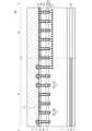
図1は、実施の形態1に係るRC-IGBT(Reverse Conducting Insulated Gate Bipolar Transistor :逆導通IGBT)である半導体装置100を示す平面図である。また、図2は、実施の形態1の他の構成のRC-IGBTである半導体装置101を示す平面図である。図1に示す半導体装置100は、IGBT領域10とダイオード領域20とがストライプ状に並んで設けられたものであり、単に「ストライプ型」と呼んでよい。図2に示す半導体装置101は、ダイオード領域20が縦方向と横方向に複数設けられ、ダイオード領域20の周囲にIGBT領域10が設けられたものであり、単に「アイランド型」と呼んでよい。
図1において、半導体装置100は、1つの半導体装置内にIGBT領域10とダイオード領域20とを備えている。IGBT領域10およびダイオード領域20は、半導体装置100の一端側から他端側に延伸し、IGBT領域10およびダイオード領域20の延伸方向と直交する方向に交互にストライプ状に設けられている。図1では、IGBT領域10を3個、ダイオード領域を2個で示し、全てのダイオード領域20がIGBT領域10で挟まれた構成で示しているが、IGBT領域10とダイオード領域20の数はこれに限るものでなく、IGBT領域10の数は3個以上でも3個以下でもよく、ダイオード領域20の数も2個以上でも2個以下でもよい。また、図1のIGBT領域10とダイオード領域20の場所を入れ替えた構成であってもよく、全てのIGBT領域10がダイオード領域20に挟まれた構成であってもよい。また、IGBT領域10とダイオード領域20とがそれぞれ1つずつ互いに隣り合って設けられた構成であってもよい。
図2において、半導体装置101は、1つの半導体装置内にIGBT領域10とダイオード領域20とを備えている。ダイオード領域20は、半導体装置内に平面視で縦方向および横方向にそれぞれ複数並んで配置されており、ダイオード領域20は周囲をIGBT領域10に取り囲まれている。つまり、IGBT領域10内に複数のダイオード領域20がアイランド状に設けられている。図2では、ダイオード領域20は紙面左右方向に4列、紙面上下方向に2行のマトリクス状に設けた構成で示しているが、ダイオード領域20の個数および配置はこれに限るものではなく、IGBT領域10内に1つまたは複数のダイオード領域20が点在して設けられ、それぞれのダイオード領域20が周囲をIGBT領域10に囲まれた構成であればよい。
図3は、図1に示した半導体装置100または図2に示した半導体装置101におけるG-G線での矢示方向断面図であり、IGBT領域10とダイオード領域20の境界部分の構成を示している。
<部分平面構成>
図8は、図1に示した半導体装置100または図2に示した半導体装置101におけるIGBT領域10の破線で囲った領域82を拡大して示す部分平面図である。図8に示すように、IGBT領域10には、アクティブトレンチゲート11とダミートレンチゲート12とがストライプ状に設けられている。半導体装置100では、アクティブトレンチゲート11およびダミートレンチゲート12は、IGBT領域10の長手方向に延伸しておりIGBT領域10の長手方向がアクティブトレンチゲート11およびダミートレンチゲート12の長手方向となっている。一方、半導体装置101では、IGBT領域10に長手方向と短手方向の区別が特段にないが、紙面左右方向をアクティブトレンチゲート11およびダミートレンチゲート12の長手方向としてもよく、紙面上下方向をアクティブトレンチゲート11およびダミートレンチゲート12の長手方向としてもよい。
図9は図8におけるA-A線での矢示方向断面図である。図9に示すIGBT領域10の断面構成は、図3に示したIGBT領域10の断面構成と基本的には同じであり、同一の構成については同一の符号を付し、重複する説明は省略するが、図9は、IGBT領域10とダイオード領域20の境界部分の断面構成ではないため、IGBT領域10にはライフタイム制御層LTの張り出し部は設けられていない。
<部分平面構成>
図11は、図1に示した半導体装置100または図2に示した半導体装置101におけるダイオード領域20の破線で囲った領域83を拡大して示す部分平面図である。図11に示すように、ダイオード領域20には、ダイオードトレンチゲート21が、半導体装置100または半導体装置101の第1主面に沿ってセル領域であるダイオード領域20の一端側から対向する他端側に向かって延伸している。ダイオードトレンチゲート21は、ダイオード領域20の半導体基板に形成されたトレンチ内にダイオードトレンチ絶縁膜21bを介してダイオードトレンチ電極21aが設けられることで構成される。ダイオードトレンチ電極21aはダイオードトレンチ絶縁膜21bを介してn-型ドリフト層1に対向している。隣接する2つのダイオードトレンチゲート21の間には、p+型コンタクト層24およびp型アノード層25が設けられている。
図12は図11におけるC-C線での矢示方向断面図である。図12に示すダイオード領域20の断面構成は、図3に示したダイオード領域20の断面構成と同じであり、同一の構成については同一の符号を付し、重複する説明は省略する。
図14は、図1に示した半導体装置100または図2に示した半導体装置101におけるE-E線での矢示方向断面図であり、IGBT領域10と終端領域30の境界部分の構成を示している。
図16は実施の形態1の変形例に係る半導体装置におけるIGBT領域10とダイオード領域20の境界部分の構成を示す断面図であり、図3に示した断面図に対応している。図16に示す断面構成と図3に示した断面構成との相違点は、IGBT領域10の第2主面側に設けられたp型コレクタ層16が、IGBT領域10とダイオード領域20との境界から距離U1だけダイオード領域20側にはみ出して設けられている点である。このように、p型コレクタ層16をダイオード領域20にはみ出して設けることにより、ダイオード領域20のn+型カソード層26とアクティブトレンチゲート11との距離を大きくすることができ、還流ダイオード動作時にアクティブトレンチゲート11にゲート駆動電圧が印加された場合であっても、IGBT領域10のアクティブトレンチゲート11に隣接して形成されるチャネルからn+型カソード層26に電流が流れるのを抑制することができる。距離U1は、例えば100μmであってよい。なお、RC-IGBTである半導体装置100または半導体装置101の用途によっては、距離U1がゼロまたは100μmより小さい距離であってもよい。
次に、製造工程を順に示す断面図である図18~図28を用いて、RC-IGBTである半導体装置100または半導体装置101の製造方法を説明する。
Claims (3)
- トランジスタとダイオードとが共通の半導体基板に形成された半導体装置であって、
前記半導体基板は、
前記トランジスタが形成されたトランジスタ領域と、
前記ダイオードが形成されたダイオード領域と、を有し、
前記トランジスタ領域は、
前記半導体基板の第2主面側に設けられた第1導電型の第1半導体層と、
前記第1半導体層上に設けられた第2導電型の第2半導体層と、
前記第2半導体層よりも前記半導体基板の第1主面側に設けられた第1導電型の第3半導体層と、
前記第3半導体層上に設けられた第2導電型の第4半導体層と、
前記第4半導体層に電気的に接続された第2電極と、
前記第1半導体層に電気的に接続された第1電極と、を備え、
前記ダイオード領域は、
前記半導体基板の前記第2主面側に設けられた第2導電型の第5半導体層と、
前記第5半導体層上に設けられた前記第2半導体層と、
前記第2半導体層よりも前記半導体基板の前記第1主面側に設けられた前記第3半導体層と、
前記第3半導体層上に設けられた第1導電型の第6半導体層と、
前記第6半導体層に電気的に接続された前記第2電極と、
前記第5半導体層に電気的に接続された前記第1電極と、
前記第1主面側からの前記第3半導体層の厚み方向端と前記第2主面側からの前記第5半導体層の厚み方向端との間の前記第2半導体層の中間位置よりも深い位置まで達する結晶欠陥層で構成されるライフタイム制御層と、を備え、
前記ライフタイム制御層は、
結晶欠陥の密度のピークが形成される深さである結晶欠陥密度最大深さが、前記中間位置よりも深い位置に設定され、前記ダイオード領域と前記トランジスタ領域との境界を跨いで前記ダイオード領域から前記トランジスタ領域に一部に張り出した張り出し部を有し、
前記第3半導体層の前記厚み方向端から前記中間位置までの厚みをt1、
前記中間位置から前記結晶欠陥密度最大深さまでの厚みをt2、とした場合に、
前記張り出し部は、
前記境界からの平面方向の張り出し幅wが、
w>((3×t1)-t2)/2となるように設定される半導体装置。 - トランジスタとダイオードとが共通の半導体基板に形成された半導体装置であって、
前記半導体基板は、
前記トランジスタが形成されたトランジスタ領域と、
前記ダイオードが形成されたダイオード領域と、を有し、
前記トランジスタ領域は、
前記半導体基板の第2主面側に設けられた第1導電型の第1半導体層と、
前記第1半導体層上に設けられた第2導電型の第2半導体層と、
前記第2半導体層よりも前記半導体基板の第1主面側に設けられた第1導電型の第3半導体層と、
前記第3半導体層上に設けられた第2導電型の第4半導体層と、
前記第4半導体層に電気的に接続された第2電極と、
前記第1半導体層に電気的に接続された第1電極と、を備え、
前記ダイオード領域は、
前記半導体基板の前記第2主面側に設けられた第2導電型の第5半導体層と、
前記第5半導体層上に設けられた前記第2半導体層と、
前記第2半導体層よりも前記半導体基板の前記第1主面側に設けられた前記第3半導体層と、
前記第3半導体層上に設けられた第1導電型の第6半導体層と、
前記第6半導体層に電気的に接続された前記第2電極と、
前記第5半導体層に電気的に接続された前記第1電極と、
前記第1主面側からの前記第3半導体層の厚み方向端と前記第2主面側からの前記第5半導体層の厚み方向端との間の前記第2半導体層の中間位置よりも深い位置まで達する結晶欠陥層で構成されるライフタイム制御層と、を備え、
前記半導体基板は、
少なくとも前記ダイオード領域および前記トランジスタ領域が設けられた領域の周囲に終端領域を有し、
前記ライフタイム制御層は、
結晶欠陥の密度のピークが形成される深さである結晶欠陥密度最大深さが、前記中間位置よりも深い位置に設定され、前記ダイオード領域と前記終端領域との境界を跨いで前記ダイオード領域から前記終端領域に一部に張り出した張り出し部を有し、
前記第3半導体層の前記厚み方向端から前記中間位置までの厚みをt1、
前記中間位置から前記結晶欠陥密度最大深さまでの厚みをt2、とした場合に、
前記張り出し部は、
前記境界からの平面方向の張り出し幅wが、
w>((3×t1)-t2)/2となるように設定される半導体装置。 - 前記ライフタイム制御層は、
前記第5半導体層には達しない深さに設定される、請求項1または請求項2記載の半導体装置。
Priority Applications (4)
| Application Number | Priority Date | Filing Date | Title |
|---|---|---|---|
| JP2020092235A JP7403386B2 (ja) | 2020-05-27 | 2020-05-27 | 半導体装置 |
| US17/168,750 US20210376167A1 (en) | 2020-05-27 | 2021-02-05 | Semiconductor device |
| DE102021107989.6A DE102021107989A1 (de) | 2020-05-27 | 2021-03-30 | Halbleitervorrichtung |
| CN202110559128.1A CN113745312A (zh) | 2020-05-27 | 2021-05-21 | 半导体装置 |
Applications Claiming Priority (1)
| Application Number | Priority Date | Filing Date | Title |
|---|---|---|---|
| JP2020092235A JP7403386B2 (ja) | 2020-05-27 | 2020-05-27 | 半導体装置 |
Publications (3)
| Publication Number | Publication Date |
|---|---|
| JP2021190496A JP2021190496A (ja) | 2021-12-13 |
| JP2021190496A5 JP2021190496A5 (ja) | 2022-06-30 |
| JP7403386B2 true JP7403386B2 (ja) | 2023-12-22 |
Family
ID=78509162
Family Applications (1)
| Application Number | Title | Priority Date | Filing Date |
|---|---|---|---|
| JP2020092235A Active JP7403386B2 (ja) | 2020-05-27 | 2020-05-27 | 半導体装置 |
Country Status (4)
| Country | Link |
|---|---|
| US (1) | US20210376167A1 (ja) |
| JP (1) | JP7403386B2 (ja) |
| CN (1) | CN113745312A (ja) |
| DE (1) | DE102021107989A1 (ja) |
Families Citing this family (2)
| Publication number | Priority date | Publication date | Assignee | Title |
|---|---|---|---|---|
| DE102022127527A1 (de) | 2022-10-19 | 2024-04-25 | Infineon Technologies Austria Ag | Rc-igbt und herstellungsverfahren für einen rc-igbt |
| CN117038451B (zh) * | 2023-10-09 | 2024-02-20 | 深圳市锐骏半导体股份有限公司 | 沟槽栅igbt器件、制作方法及仿真方法 |
Citations (4)
| Publication number | Priority date | Publication date | Assignee | Title |
|---|---|---|---|---|
| JP2011216825A (ja) | 2010-04-02 | 2011-10-27 | Toyota Central R&D Labs Inc | 半導体装置 |
| JP2015118991A (ja) | 2013-12-17 | 2015-06-25 | トヨタ自動車株式会社 | 半導体装置 |
| JP2016162950A (ja) | 2015-03-04 | 2016-09-05 | トヨタ自動車株式会社 | 半導体装置 |
| WO2019098270A1 (ja) | 2017-11-15 | 2019-05-23 | 富士電機株式会社 | 半導体装置 |
Family Cites Families (4)
| Publication number | Priority date | Publication date | Assignee | Title |
|---|---|---|---|---|
| JP2011210800A (ja) * | 2010-03-29 | 2011-10-20 | Toyota Motor Corp | 半導体装置 |
| JP6078961B2 (ja) * | 2012-03-19 | 2017-02-15 | 富士電機株式会社 | 半導体装置の製造方法 |
| JP6107767B2 (ja) * | 2013-12-27 | 2017-04-05 | トヨタ自動車株式会社 | 半導体装置とその製造方法 |
| WO2019159391A1 (ja) * | 2018-02-14 | 2019-08-22 | 富士電機株式会社 | 半導体装置 |
-
2020
- 2020-05-27 JP JP2020092235A patent/JP7403386B2/ja active Active
-
2021
- 2021-02-05 US US17/168,750 patent/US20210376167A1/en active Pending
- 2021-03-30 DE DE102021107989.6A patent/DE102021107989A1/de active Pending
- 2021-05-21 CN CN202110559128.1A patent/CN113745312A/zh active Pending
Patent Citations (4)
| Publication number | Priority date | Publication date | Assignee | Title |
|---|---|---|---|---|
| JP2011216825A (ja) | 2010-04-02 | 2011-10-27 | Toyota Central R&D Labs Inc | 半導体装置 |
| JP2015118991A (ja) | 2013-12-17 | 2015-06-25 | トヨタ自動車株式会社 | 半導体装置 |
| JP2016162950A (ja) | 2015-03-04 | 2016-09-05 | トヨタ自動車株式会社 | 半導体装置 |
| WO2019098270A1 (ja) | 2017-11-15 | 2019-05-23 | 富士電機株式会社 | 半導体装置 |
Also Published As
| Publication number | Publication date |
|---|---|
| US20210376167A1 (en) | 2021-12-02 |
| CN113745312A (zh) | 2021-12-03 |
| JP2021190496A (ja) | 2021-12-13 |
| DE102021107989A1 (de) | 2021-12-02 |
Similar Documents
| Publication | Publication Date | Title |
|---|---|---|
| US11276773B2 (en) | Semiconductor device | |
| US11495678B2 (en) | Semiconductor device | |
| US20220084825A1 (en) | Semiconductor device and method of manufacturing semiconductor device | |
| US11456376B2 (en) | Semiconductor device | |
| JP7403386B2 (ja) | 半導体装置 | |
| US20220238513A1 (en) | Semiconductor device and method for manufacturing the same | |
| CN111370481A (zh) | 功率器件及功率器件制备方法 | |
| JP7332543B2 (ja) | 半導体装置 | |
| JP7403401B2 (ja) | 半導体装置 | |
| JP7475265B2 (ja) | 半導体装置及び半導体装置の製造方法 | |
| JP2022056498A (ja) | 半導体装置 | |
| US20240047454A1 (en) | Semiconductor device and method for manufacturing semiconductor device | |
| US20230083162A1 (en) | Semiconductor device | |
| US20230126799A1 (en) | Semiconductor device and method for manufacturing semiconductor device | |
| US20240072043A1 (en) | Semiconductor device and method of manufacturing semiconductor device | |
| JP7486407B2 (ja) | 半導体装置および半導体装置の製造方法 | |
| US20220173094A1 (en) | Semiconductor device and method of manufacturing semiconductor device | |
| JP7486373B2 (ja) | 半導体装置 | |
| CN211350662U (zh) | 功率器件 | |
| CN114725184A (zh) | 半导体装置 | |
| JP2022035157A (ja) | 半導体装置および半導体装置の製造方法 | |
| CN114447097A (zh) | 半导体装置 |
Legal Events
| Date | Code | Title | Description |
|---|---|---|---|
| A521 | Request for written amendment filed |
Free format text: JAPANESE INTERMEDIATE CODE: A523 Effective date: 20220622 |
|
| A621 | Written request for application examination |
Free format text: JAPANESE INTERMEDIATE CODE: A621 Effective date: 20220622 |
|
| A131 | Notification of reasons for refusal |
Free format text: JAPANESE INTERMEDIATE CODE: A131 Effective date: 20230620 |
|
| A977 | Report on retrieval |
Free format text: JAPANESE INTERMEDIATE CODE: A971007 Effective date: 20230622 |
|
| A521 | Request for written amendment filed |
Free format text: JAPANESE INTERMEDIATE CODE: A523 Effective date: 20230801 |
|
| TRDD | Decision of grant or rejection written | ||
| A01 | Written decision to grant a patent or to grant a registration (utility model) |
Free format text: JAPANESE INTERMEDIATE CODE: A01 Effective date: 20231114 |
|
| A61 | First payment of annual fees (during grant procedure) |
Free format text: JAPANESE INTERMEDIATE CODE: A61 Effective date: 20231212 |
|
| R150 | Certificate of patent or registration of utility model |
Ref document number: 7403386 Country of ref document: JP Free format text: JAPANESE INTERMEDIATE CODE: R150 |