JP7365528B2 - Bonded substrate, circuit board and method for manufacturing the same, individual board and method for manufacturing the same - Google Patents
Bonded substrate, circuit board and method for manufacturing the same, individual board and method for manufacturing the same Download PDFInfo
- Publication number
- JP7365528B2 JP7365528B2 JP2023506314A JP2023506314A JP7365528B2 JP 7365528 B2 JP7365528 B2 JP 7365528B2 JP 2023506314 A JP2023506314 A JP 2023506314A JP 2023506314 A JP2023506314 A JP 2023506314A JP 7365528 B2 JP7365528 B2 JP 7365528B2
- Authority
- JP
- Japan
- Prior art keywords
- identification mark
- conductor
- dummy
- circuit board
- bonded substrate
- Prior art date
- Legal status (The legal status is an assumption and is not a legal conclusion. Google has not performed a legal analysis and makes no representation as to the accuracy of the status listed.)
- Active
Links
Images


Classifications
-
- H—ELECTRICITY
- H05—ELECTRIC TECHNIQUES NOT OTHERWISE PROVIDED FOR
- H05K—PRINTED CIRCUITS; CASINGS OR CONSTRUCTIONAL DETAILS OF ELECTRIC APPARATUS; MANUFACTURE OF ASSEMBLAGES OF ELECTRICAL COMPONENTS
- H05K1/00—Printed circuits
- H05K1/02—Details
-
- H—ELECTRICITY
- H05—ELECTRIC TECHNIQUES NOT OTHERWISE PROVIDED FOR
- H05K—PRINTED CIRCUITS; CASINGS OR CONSTRUCTIONAL DETAILS OF ELECTRIC APPARATUS; MANUFACTURE OF ASSEMBLAGES OF ELECTRICAL COMPONENTS
- H05K3/00—Apparatus or processes for manufacturing printed circuits
Description
本開示は、接合基板、回路基板及びその製造方法、並びに、個片基板及びその製造方法に関する。 The present disclosure relates to a bonded substrate, a circuit board, and a manufacturing method thereof, and an individual board and a manufacturing method thereof.
電子デバイスに搭載される個片基板には、絶縁性のセラミック基板が用いられる場合がある。このような個片基板を得るための多数個取り配線基板としては、複数の配線基板領域を縦横に配列するとともに外周部にダミー領域を設け、各配線基板領域の内層に空隙からなる記号パターンを備えるものが知られている(例えば、特許文献1)。このような記号パターンを、超音波探傷装置又はX線等を用いて解析すれば、配線基板領域の配列位置を検知することができる。 Insulating ceramic substrates are sometimes used as individual substrates mounted on electronic devices. A multi-chip wiring board for obtaining such individual boards has a plurality of wiring board areas arranged vertically and horizontally, a dummy area is provided on the outer periphery, and a symbol pattern consisting of voids is formed in the inner layer of each wiring board area. Some devices are known (for example, Patent Document 1). By analyzing such a symbol pattern using an ultrasonic flaw detector, X-rays, or the like, it is possible to detect the arrangement position of the wiring board area.
また、個片基板の材料に用いられるセラミックグリーンシートの一部にレーザ光を照射してバーコード又は二次元コードを描画する工程と、このセラミックグリーンシートを焼成して、複数の基板形成領域を備えるセラミック基板を得る工程と、セラミック基板を分割する工程とを有する製造方法が知られている(例えば、特許文献2及び3)。これによって、成形ロット番号と最終製品とを紐づけることができる。 In addition, there is a step of irradiating a part of the ceramic green sheet used as the material for the individual substrates with a laser beam to draw a barcode or two-dimensional code, and a step of firing the ceramic green sheet to form multiple substrate forming areas. A manufacturing method is known that includes a step of obtaining a ceramic substrate and a step of dividing the ceramic substrate (for example, Patent Documents 2 and 3). This allows the molding lot number and the final product to be linked.
特許文献1~3に記載されるような記号パターン及び二次元コード等の識別マークは、トレーサビリティを図るうえで有用であると考えられる。そこで、本開示は、トレーサビリティに優れる回路基板及びその製造方法を提供する。また、トレーサビリティに優れる接合基板を提供する。また、トレーサビリティに優れる個片基板及びその製造方法を提供する。
Identification marks such as symbol patterns and two-dimensional codes as described in
本開示は、幾つかの側面において[1]~[13]を提供する。
[1]回路形成部とダミー部とを備える回路基板であって、
セラミック板と、前記セラミック板の主面に接合されている複数の導体部と、を備え、
前記複数の導体部は、前記ダミー部に設けられる第1導体部と、前記回路形成部に設けられる第2導体部と、を含み、
前記第1導体部の表面に第1識別マークを有する、回路基板。
[2]前記回路形成部を取り囲む前記ダミー部における前記第1導体部の外縁の一部は、前記セラミック板の前記主面よりも外側にはみ出している、[1]に記載の回路基板。
[3]前記複数の導体部は、前記ダミー部に設けられ、前記第1識別マークを有しない第3導体部を含む、[1]又は[2]に記載の回路基板。
[4]前記第2導体部の表面に第2識別マークを有し、当該第2識別マークは、前記第1識別マークに含まれる第1情報に関連する第2情報を含む、[1]~[3]のいずれか一つに記載の回路基板。
[5]前記第1識別マークは、レーザ孔で構成されるコードを含み、前記レーザ孔は1μm以上の深さを有する、[1]~[4]のいずれか一つに記載の回路基板。
[6]回路形成領域とダミー領域とを含む主面を有するセラミック板と、前記主面を覆うように前記セラミック板に接合される金属板と、を備える接合基板であって、前記金属板は、前記ダミー領域を覆う部分の表面に第3識別マークを有する、接合基板。
[7]前記金属板の外縁の一部は前記セラミック板の前記主面よりも外側にはみ出しており、前記セラミック板の角部は前記金属板よりも外側に突出している、[6]に記載の接合基板。
[8]前記回路形成領域を覆う部分の表面に第4識別マークを有し、当該第4識別マークは、前記第3識別マークに含まれる第3情報に関連する第4情報を含む、[6]又は[7]に記載の接合基板。
[9]前記第3識別マークは、レーザ孔で構成されるコードを含み、前記レーザ孔は3μm以上の深さを有する、[6]~[8]のいずれか一つに記載の接合基板。
[10]第1導体部を有するダミー部と第2導体部を有する回路形成部とを備える回路基板から前記ダミー部を切り離して得られる、前記第2導体部を有する個片基板であって、
前記第2導体部の表面は、前記第1導体部の表面における第1識別マークに含まれる第1情報に関連する第2情報を含む第2識別マークを有する、個片基板。
[11]前記第2識別マークは、レーザ孔で構成されるコードを含み、前記レーザ孔は1μm以上の深さを有する、[10]に記載の個片基板。
[12]前記[6]~[9]のいずれか一つの接合基板に少なくともエッチング処理を施して、前記ダミー領域及び前記回路形成領域に、第1導体部及び第2導体部をそれぞれ形成し、前記第1導体部を含むダミー部と前記第2導体部を含む回路形成部とを有する回路基板を得る工程を有し、
前記第1導体部の表面は、前記第3識別マークに由来する第1識別マークを有する、回路基板の製造方法。
[13]前記[6]~[9]のいずれか一つの接合基板に少なくともエッチング処理を施して、前記ダミー領域及び前記回路形成領域に、第1導体部及び第2導体部をそれぞれ形成し、前記第1導体部を含むダミー部と前記第2導体部を含む回路形成部とを有する回路基板を得る工程と、
前記回路基板から前記ダミー部を切り離し、前記第2導体部を有する個片基板を得る工程と、を有し、
前記第1導体部の表面は、前記第3識別マークに由来する第1識別マークを有する、個片基板の製造方法。The present disclosure provides [1] to [13] in some aspects.
[1] A circuit board comprising a circuit forming part and a dummy part,
comprising a ceramic plate and a plurality of conductor parts joined to the main surface of the ceramic plate,
The plurality of conductor parts include a first conductor part provided in the dummy part and a second conductor part provided in the circuit forming part,
A circuit board having a first identification mark on a surface of the first conductor portion.
[2] The circuit board according to [1], wherein a part of the outer edge of the first conductor part in the dummy part surrounding the circuit forming part protrudes outside the main surface of the ceramic board.
[3] The circuit board according to [1] or [2], wherein the plurality of conductor parts include a third conductor part that is provided in the dummy part and does not have the first identification mark.
[4] A second identification mark is provided on the surface of the second conductor portion, and the second identification mark includes second information related to the first information included in the first identification mark, [1] to The circuit board according to any one of [3].
[5] The circuit board according to any one of [1] to [4], wherein the first identification mark includes a code formed of a laser hole, and the laser hole has a depth of 1 μm or more.
[6] A bonded substrate comprising: a ceramic plate having a main surface including a circuit forming area and a dummy area; and a metal plate bonded to the ceramic plate so as to cover the main surface, the metal plate comprising: , a bonded substrate having a third identification mark on a surface of a portion covering the dummy region;
[7] According to [6], a part of the outer edge of the metal plate protrudes outward from the main surface of the ceramic plate, and a corner of the ceramic plate protrudes outward from the metal plate. bonded substrate.
[8] A fourth identification mark is provided on the surface of the portion covering the circuit formation area, and the fourth identification mark includes fourth information related to the third information included in the third identification mark, [6 ] or the bonded substrate according to [7].
[9] The bonded substrate according to any one of [6] to [8], wherein the third identification mark includes a code formed of a laser hole, and the laser hole has a depth of 3 μm or more.
[10] An individual board having the second conductor portion obtained by separating the dummy portion from a circuit board comprising a dummy portion having the first conductor portion and a circuit forming portion having the second conductor portion,
The surface of the second conductor section has a second identification mark including second information related to the first information included in the first identification mark on the surface of the first conductor section.
[11] The individual substrate according to [10], wherein the second identification mark includes a code formed of a laser hole, and the laser hole has a depth of 1 μm or more.
[12] Performing at least an etching process on the bonded substrate according to any one of [6] to [9] to form a first conductor portion and a second conductor portion in the dummy region and the circuit formation region, respectively; obtaining a circuit board having a dummy part including the first conductor part and a circuit forming part including the second conductor part;
The method for manufacturing a circuit board, wherein the surface of the first conductor portion has a first identification mark derived from the third identification mark.
[13] Performing at least an etching process on the bonded substrate according to any one of [6] to [9] to form a first conductor portion and a second conductor portion in the dummy region and the circuit formation region, respectively; obtaining a circuit board having a dummy part including the first conductor part and a circuit forming part including the second conductor part;
separating the dummy portion from the circuit board to obtain individual boards having the second conductor portion;
A method for manufacturing an individual substrate, wherein a surface of the first conductor portion has a first identification mark derived from the third identification mark.
上記[1]の回路基板は、第1識別マークを有する第1導体部をダミー部に設けることによって、回路形成部に識別マークを設けなくてもトレーサビリティを確保することができる。また、第1導体部の表面に第1識別マークを有するため、回路基板の内部に識別マークが設けられる場合に比べて読み取り精度を高くすることができる。このため、上記回路基板はトレーサビリティに優れる。 In the circuit board of [1] above, by providing the first conductor portion having the first identification mark on the dummy portion, traceability can be ensured without providing the identification mark on the circuit forming portion. Further, since the first identification mark is provided on the surface of the first conductor portion, reading accuracy can be increased compared to a case where the identification mark is provided inside the circuit board. Therefore, the circuit board has excellent traceability.
上記回路基板は[2]の構成を有していてもよい。これによって、第1導体部とセラミック板の主面とがろう材層を介して接合されている場合であっても、ろう材が第1導体部の表面に染み出して第1識別マークが汚染されることを抑制できる。したがって、第1識別マークの読み取り精度を十分に高く維持することができる。 The circuit board may have the configuration [2]. As a result, even if the first conductor part and the main surface of the ceramic plate are bonded via the brazing metal layer, the brazing metal seeps onto the surface of the first conductor part and contaminates the first identification mark. It is possible to prevent this from happening. Therefore, the reading accuracy of the first identification mark can be maintained sufficiently high.
上記回路基板は[3]の構成を有していてもよい。第3導体部を含むことによって、エッチングによって第1導体部及び第2導体部を形成するときに、エッチング速度のばらつきを低減し、回路形成部に設けられる第2導体部の形状の均一性を向上することができる。 The circuit board may have the configuration [3]. By including the third conductor part, when forming the first conductor part and the second conductor part by etching, it is possible to reduce variations in etching speed and improve the uniformity of the shape of the second conductor part provided in the circuit forming part. can be improved.
上記回路基板は[4]の構成を有していてもよい。このような回路基板は、第2導体部の表面に第2識別マークを有するため、回路形成部の内部に識別マークが設けられる場合に比べて読み取り精度を高くすることができる。また、第2識別マークは、第1識別マークに含まれる第1情報に関連する第2情報を含んでいるため、回路基板からダミー部を切り離して得られる回路形成部(個片基板)のトレーサビリティも確保することができる。また、回路基板と、回路基板からダミー部を切り離して得られる回路形成部(個片基板)とを紐づけて管理することができる。したがって、トレーサビリティの範囲を拡張することができる。 The circuit board may have the configuration [4]. Since such a circuit board has the second identification mark on the surface of the second conductor part, it is possible to improve the reading accuracy compared to a case where the identification mark is provided inside the circuit forming part. In addition, since the second identification mark includes second information related to the first information included in the first identification mark, traceability of the circuit forming part (individual board) obtained by separating the dummy part from the circuit board is improved. can also be secured. Further, the circuit board and the circuit forming part (individual board) obtained by separating the dummy part from the circuit board can be linked and managed. Therefore, the range of traceability can be expanded.
上記回路基板は[5]の構成を有していてもよい。これによって、表面処理を行っても、読み取り精度を十分に維持することができる。したがって、トレーサビリティの信頼性を十分に高くすることができる。 The circuit board may have the configuration [5]. Thereby, even if surface treatment is performed, reading accuracy can be maintained sufficiently. Therefore, the reliability of traceability can be made sufficiently high.
上記[6]の接合基板は、金属板の表面に第3識別マークを有することから、トレーサビリティに優れる。また、金属板は、ダミー領域を覆う部分の表面に第3識別マークを有することから、回路形成部となる部分に識別マークを設けなくてもトレーサビリティを確保することができる。 The bonded substrate of [6] above has excellent traceability because it has the third identification mark on the surface of the metal plate. Further, since the metal plate has the third identification mark on the surface of the portion covering the dummy region, traceability can be ensured without providing an identification mark on the portion that will become the circuit forming portion.
上記接合基板は[7]の構成を有していてもよい。金属板の外縁の一部がセラミック板の主面からはみ出していることによって、金属板とセラミック板の主面とがろう材層を介して接合されている場合であっても、ろう材が金属板の表面に染み出して第3識別マークが被覆されることを抑制できる。したがって、第3識別マークの読み取り精度を十分に高く維持することができる。また、セラミック板の角部が露出していることによって、当該角部を用いて位置合わせを行うことができる。このような接合基板、並びに、これから得られる回路基板及び個片基板は、寸法精度に優れる。 The bonded substrate may have the configuration [7]. Because a part of the outer edge of the metal plate protrudes from the main surface of the ceramic plate, even if the main surfaces of the metal plate and the ceramic plate are joined via a brazing material layer, the brazing material may It is possible to prevent the third identification mark from seeping onto the surface of the board and covering it. Therefore, the reading accuracy of the third identification mark can be maintained sufficiently high. Furthermore, since the corners of the ceramic plate are exposed, alignment can be performed using the corners. Such a bonded substrate, as well as circuit boards and individual substrates obtained therefrom, have excellent dimensional accuracy.
上記接合基板は[8]の構成を有していてもよい。これによって、トレーサビリティの範囲を拡張することができる。例えば、エッチングによって、ダミー部と回路形成部とを形成し、これらを切り離した後もトレーサビリティを確保することができる。 The bonded substrate may have the configuration [8]. This allows the range of traceability to be expanded. For example, by forming a dummy part and a circuit forming part by etching, traceability can be ensured even after they are separated.
上記接合基板は[9]の構成を有していてもよい。これによって、接合基板に表面処理及びエッチング処理を施した後であっても、第3識別マークに由来する識別マークの読み取り精度を十分に維持することができる。これによって、トレーサビリティの信頼性を十分に高くすることができる。 The bonded substrate may have the configuration [9]. Thereby, even after surface treatment and etching treatment are performed on the bonded substrate, the reading accuracy of the identification mark derived from the third identification mark can be sufficiently maintained. This makes it possible to sufficiently increase the reliability of traceability.
上記[10]の個片基板は、第2導体部における表面に第2識別マークを有する。このような第2識別マークは、個片基板の内部に識別マークが設けられる場合に比べて読み取り精度を高くすることができる。また、第2識別マークは第1識別マークに含まれる第1情報に関連する第2情報を含むことから、回路基板又はダミー部と、個片基板とを紐づけて管理することが可能となり、トレーサビリティの範囲を拡張することができる。したがって、上記個片基板はトレーサビリティに優れる。 The individual substrate of [10] above has a second identification mark on the surface of the second conductor portion. Such a second identification mark can improve the reading accuracy compared to the case where the identification mark is provided inside the individual substrate. In addition, since the second identification mark includes second information related to the first information included in the first identification mark, it becomes possible to manage the circuit board or dummy part and the individual board by linking them, The scope of traceability can be expanded. Therefore, the individual substrates have excellent traceability.
上記個片基板は[11]の構成を有していてもよい。これによって、読み取り精度を向上してトレーサビリティの信頼性を十分に高くすることができる。 The individual substrate may have the configuration [11]. Thereby, reading accuracy can be improved and traceability reliability can be made sufficiently high.
上記[12]の回路基板の製造方法では、接合基板が金属板の表面に第3識別マークを有し、回路基板が第1導体部の表面に第3識別マークに由来する第1識別マークを有する。このため、接合基板から回路基板までのトレーサビリティを確保することができる。また、第1識別マーク及び第3識別マークは、導体部及び金属板の表面に設けられることから読み取り精度に優れる。したがって、上記回路基板の製造方法は、トレーサビリティに優れる。 In the method for manufacturing a circuit board according to [12] above, the bonded substrate has a third identification mark on the surface of the metal plate, and the circuit board has a first identification mark derived from the third identification mark on the surface of the first conductor portion. have Therefore, traceability from the bonded substrate to the circuit board can be ensured. Further, since the first identification mark and the third identification mark are provided on the surface of the conductor portion and the metal plate, the reading accuracy is excellent. Therefore, the above method for manufacturing a circuit board has excellent traceability.
上記[13]の個片基板の製造方法では、接合基板が金属板の表面に第3識別マークを有し、回路基板が第1導体部の表面に第3識別マークに由来する第1識別マークを有する。このため、接合基板から回路基板までのトレーサビリティを確保することができる。また、第1識別マーク及び第3識別マークは読み取り精度に優れる。したがって、上記個片基板の製造方法は、トレーサビリティに優れる。 In the method for manufacturing an individual board according to [13] above, the bonded substrate has a third identification mark on the surface of the metal plate, and the circuit board has a first identification mark derived from the third identification mark on the surface of the first conductor part. has. Therefore, traceability from the bonded substrate to the circuit board can be ensured. Further, the first identification mark and the third identification mark have excellent reading accuracy. Therefore, the above method for manufacturing individual substrates has excellent traceability.
トレーサビリティに優れる回路基板及びその製造方法を提供することができる。また、トレーサビリティに優れる接合基板を提供することができる。また、トレーサビリティに優れる個片基板及びその製造方法を提供することができる。 A circuit board with excellent traceability and a method for manufacturing the same can be provided. Furthermore, a bonded substrate with excellent traceability can be provided. Further, it is possible to provide an individual substrate with excellent traceability and a method for manufacturing the same.
以下、場合により図面を参照して、本開示の一実施形態について説明する。ただし、以下の実施形態は、本開示を説明するための例示であり、本開示を以下の内容に限定する趣旨ではない。説明において、同一要素又は同一機能を有する要素には同一符号を用い、場合により重複する説明は省略する。また、上下左右等の位置関係は、特に断らない限り、図面に示す位置関係に基づくものとする。各要素の寸法比率は図示の比率に限られるものではない。本明細書に明示される数値範囲の上限値又は下限値は、実施例に示されるいずれかの値に置き換えてもよい。また、個別に記載した上限値及び下限値は任意に組み合わせてもよい。 Hereinafter, one embodiment of the present disclosure will be described with reference to the drawings as the case may be. However, the following embodiments are examples for explaining the present disclosure, and are not intended to limit the present disclosure to the following contents. In the description, the same reference numerals will be used for the same elements or elements having the same function, and redundant description will be omitted in some cases. In addition, the positional relationships such as top, bottom, left, and right are based on the positional relationships shown in the drawings unless otherwise specified. The dimensional ratio of each element is not limited to the illustrated ratio. The upper limit or lower limit of the numerical range specified herein may be replaced with any value shown in the Examples. Moreover, the upper limit value and lower limit value described individually may be combined arbitrarily.
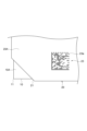
図1は、一実施形態に係る接合基板100の斜視図である。図1の接合基板100は、セラミック板10と、セラミック板10の両方の主面をそれぞれ覆うようにセラミック板10に接合されている一対の金属板20,30と、を備える。一対の金属板20,30は例えば銅板又はアルミニウム板であってよい。接合基板100は、金属板20の表面20Aに、第3識別マーク23を有する。金属板30の表面にも、同様の識別マークを有していてもよいし、有していなくてもよい。表面20Aには、2つの第3識別マーク23が示されているが、その数は限定されず、1つであってもよいし、3つ以上であってもよい。
FIG. 1 is a perspective view of a bonded
第3識別マーク23は、金属板20及び接合基板100を識別可能なものであればよい。例えば、バーコード等の一次元コードであってよく、二次元コードであってもよい。第3識別マーク23は、表面20Aに印刷されたものであってよく、凹凸形状で構成されたものであってもよい。例えば、凹部と模様が組み合わされたものであってもよい。複数ある第3識別マーク23は、互いに同じであってよく、異なっていてもよい。
The
第3識別マーク23は、例えば、カメラ又はビデオ等の撮像装置によって検出可能に構成される。撮像装置は、例えば撮像した画像と予め記録された情報とを照合し、照合結果に基づいて情報を出力する情報処理部を有していてよい。本開示における他の識別マークも同様であってよい。
The
第3識別マーク23は、接合基板100及び後述の回路基板200を識別するために用いられてよい。また、接合基板100を作製する前に、金属板20,30の表面に設けておけば、金属板20,30を識別することができる。第3識別マーク23は何らかの情報と関連付けられたコードであってよい。情報としては、例えば、ロット、製造履歴、製品の種類、用途、品質、及び製造条件に関するものが挙げられる。第3識別マーク23を用いることによって、金属板20,30、接合基板100及びこれから得られる各種生産品のトレーサビリティを向上することができる。例えば、第3識別マーク23を用いて、品質管理及び工程管理を行ってよい。
The
第3識別マーク23は、例えば、以下(a),(b),(c),(d),(e)及び(f)の情報のうち1又は2以上がコード化されたものであってよい。
(a)金属板に関する情報
(b)接合基板の製造情報(製造日、製造条件、及び製造設備等)
(c)接合基板の品質情報
(d)接合基板の表面処理条件
(e)接合基板のエッチング条件
(f)接合基板のシリアル番号The
(a) Information regarding the metal plate (b) Manufacturing information of the bonded substrate (manufacturing date, manufacturing conditions, manufacturing equipment, etc.)
(c) Quality information of the bonded substrate (d) Surface treatment conditions of the bonded substrate (e) Etching conditions of the bonded substrate (f) Serial number of the bonded substrate
図2は、第3識別マーク23の一例を示す図である。第3識別マーク23は、二次元コードであり、複数の凹部23aが所定の規則に従って並んで構成される。第3識別マーク23は、例えばQRコード(登録商標)等の二次元バーコードであってよい。また、例えば凹部23aの深さに関する情報も利用して三次元コードとしてもよい。凹部23aは、レーザ光によって形成されるレーザ孔であってよい。レーザ源としては、例えば、炭酸ガスレーザ及びYAGレーザ等を用いることができる。なお、第3識別マーク23は、凹部23aで構成されるものに限定されない。
FIG. 2 is a diagram showing an example of the
第3識別マーク23を構成する凹部23aの深さは3μm以上であってよく、5μm以上であってもよい。これによって、化学研磨等の表面処理を施した後も、十分な読み取り精度を確保することができる。凹部23aの深さは、50μm以下であってよく、30μm以下であってよく、10μm未満であってもよい。このように深さを小さくすることによって、レーザ孔を形成する時間を短縮するとともに、レーザ孔の形成に伴う異物(ドロス)の発生量を低減することができる。
The depth of the recessed
第3識別マーク23のコードサイズは、平面視で、各辺の長さが1~4mmであってよい。これによって、撮像装置による検知精度を十分に維持しつつ、後述するセラミック板10のダミー領域15を覆う部分の表面に十分に収まるサイズとすることができる。このようなサイズとしつつ情報量を確保する観点から、セル数(一方向に沿って並ぶ凹部23aの最大数)は、5~30であってよく、10~20であってよい。
The code size of the
図3の断面図に示すように、金属板20及び金属板30は、ろう材層52及び53を介して、セラミック板10の主面10A及び主面10Bにそれぞれ接合されている。金属板20及び金属板30の外縁27及び外縁37は、セラミック板10の主面10A及び主面10Bよりも外側にはみ出している。これによって、金属板20の表面20A及び金属板30の表面30Aに、ろう材成分がしみ出すことを抑制できる。したがって、金属板20の表面20Aの第3識別マーク23がろう材成分で覆われることを抑制できる。このような第3識別マーク23は読み取り精度に優れる。また、金属板30の表面30Aに識別マークを設けた場合も、当該識別マークがろう材成分で覆われることを抑制できる。
As shown in the cross-sectional view of FIG. 3,
図3では、ろう材層52,53は、回路基板を作製したときの導体部となる部分に対応する部分にのみ設けられている。すなわち、隣り合うろう材層の間には空隙部がある。変形例では、このような空隙部を設けなくてもよい。 In FIG. 3, brazing material layers 52 and 53 are provided only in portions corresponding to portions that will become conductor portions when the circuit board is manufactured. That is, there are voids between adjacent brazing filler metal layers. In a modified example, such a gap may not be provided.
図4に示すように、セラミック板10の主面10Aは、矩形であり、区画線によって複数に区画されている。主面10Aには、区画線として、第1の方向に沿って延在し且つ等間隔で並ぶ複数の区画線L1と、第1の方向に直交する第2の方向に沿って延在し且つ等間隔で並ぶ複数の区画線L2と、が設けられている。区画線L1と区画線L2とは互いに直交している。
As shown in FIG. 4, the
区画線L1,L2は、例えば、複数の凹みが直線状に並んで構成されていてもよいし、線状に溝が形成されていてもよい。具体的には、レーザ光で形成されるスクライブラインであってよい。レーザ源としては、例えば、炭酸ガスレーザ及びYAGレーザ等が挙げられる。このようなレーザ源からレーザ光を間欠的に照射することによってスクライブラインを形成することができる。なお、区画線L1,L2は、等間隔で並んでいなくてもよく、また、直交するものに限定されない。また、直線状ではなく、曲線状であってもよいし、折れ曲がっていてもよい。図4には、セラミック板10の一方の主面10Aのみに区画線L1,L2が設けられているが、セラミック板10の他方の主面10Bにも、区画線L1,L2が形成されていてもよい。
The partition lines L1 and L2 may be formed by, for example, a plurality of recesses lined up in a straight line, or may have a linear groove formed therein. Specifically, it may be a scribe line formed by laser light. Examples of the laser source include a carbon dioxide laser and a YAG laser. A scribe line can be formed by intermittently irradiating laser light from such a laser source. Note that the partition lines L1 and L2 do not have to be arranged at equal intervals, and are not limited to being perpendicular to each other. Moreover, the shape may not be straight, but may be curved or bent. In FIG. 4, partition lines L1 and L2 are provided only on one
図4に示すように、セラミック板10は、最も外側に配置される2本の区画線L1及び最も外側に配置される2本の区画線L2によって画定される、6個の区画部18を含む回路形成領域16と、回路形成領域16を取り囲むダミー領域15と有する。6個の区画部18には、それぞれ回路となる導体部が形成されてよい。図1の接合基板100における金属板20は、表面20Aのうち、セラミック板10のダミー領域15を覆う部分の表面に第3識別マーク23を有する。すなわち、図1及び図2に示す第3識別マーク23は、セラミック板10のダミー領域15の上方に設けられる。一方、金属板20は、表面20Aのうち、セラミック板10の回路形成領域16を覆う部分の表面に識別マークを有しない。これによって、セラミック板10の回路形成領域16に設けられる、回路となる導体部と主面10Aとの接合状態を検査する際に、識別マークが障害となることを回避できる。したがって、導体部の接合状態の検査精度を十分に高くすることができる。これによって、信頼性に優れる回路基板及び個片基板を得ることができる。
As shown in FIG. 4, the
図1に示すように、接合基板100において、セラミック板10の角部11は、一対の金属板20,30よりも外側に突出している。一対の金属板20,30は、それぞれ4つの角部が面取り加工されている。一対の金属板20,30の面取り部26,36の間から、セラミック板10の角部11が露出している。面取り部26,36の形状は特に限定されず、例えば、C面取り形状であってもよいし、R面取り形状であってもよい。一対の金属板20,30の形状は同じであってよく、異なっていてもよい。
As shown in FIG. 1, in the bonded
セラミック板10の角部11の位置は、接合基板100を平面視したときに、容易に検知することができる。このため、角部11を接合基板100の位置合わせの基準とすることによって、接合基板100の加工を円滑に且つ高精度に行うことができる。その結果、寸法精度に優れる加工品を円滑に製造することができる。
The position of the
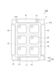
図5及び図6に示す回路基板200からは、セラミック板10を区画線L1,L2に沿って分割することによって、複数の個片基板が得られる。この場合、セラミック板10は、図6示す仮想線VLに沿って切断される。このような回路基板200は、多数個取り回路基板とも称される。回路基板200は、図1の接合基板100を加工して得てもよい。回路基板200は、セラミック板10の回路形成領域16を含む回路形成部216と、セラミック板10のダミー領域15を含むダミー部215とを備える。回路形成部216は、主面10A,10B上に、それぞれ6個の第2導体部42を有している。複数の第2導体部42は、区画部18毎に独立して設けられている。
From the
図5に示すように、回路形成部216を取り囲むダミー部215は、第1導体部41及び第3導体部43を有している。第1導体部41及び第3導体部43は、セラミック板10の矩形の主面10Aの外縁をなす各辺に沿って合計4個設けられている。このうち、主面10A上において互いに対向する2個の第1導体部41は、表面に第1識別マーク21を有する。回路基板200が接合基板100を加工して得られるものである場合、第1識別マーク21は、図1の第3識別マーク23に由来するものであってよい。すなわち、第1識別マーク21と第3識別マーク23は全く同じものであってもよいし、接合基板100から回路基板200を得るための加工プロセスを得ることによって、変色したり変形したりしたものであってもよい。第1識別マーク21及び第3識別マーク23の形状及び機能は同じであってよい。
As shown in FIG. 5, the
第1識別マーク21は、回路基板200を識別可能なものであればよい。例えば、バーコード等の一次元コードであってよく、二次元コードであってもよい。第1識別マーク21は、第1導体部41の表面に印刷されたものであってよく、凹凸形状で構成されたものであってもよい。例えば、凹部と模様が組み合わされたものであってもよい。複数ある第1識別マーク21は、互いに同じであってよく、異なっていてもよい。
The
第1識別マーク21は、回路基板200を識別するために用いられてよい。第1識別マーク21は何らかの情報と関連付けられたコードであってよい。情報としては、例えば、ロット、製造履歴、製品の種類、用途、品質、及び製造条件に関するものが挙げられる。第1識別マーク21を用いることによって、回路基板200のトレーサビリティを向上することができる。第1識別マーク21を用いて、品質管理及び工程管理を行ってよい。
The
第1識別マーク21は、例えば、以下(a),(b),(c)及び(d)の情報のうち1又は2以上がコード化されたものであってよい。
(a)用いた接合基板の情報(金属板の情報)
(b)回路基板の製造情報(製造日、製造条件、及び製造設備等)
(c)回路基板の品質情報
(d)回路基板の分割条件The
(a) Information on the bonded substrate used (information on the metal plate)
(b) Manufacturing information of circuit board (manufacturing date, manufacturing conditions, manufacturing equipment, etc.)
(c) Quality information of the circuit board (d) Conditions for dividing the circuit board
回路基板200の第1識別マーク21は、第1導体部41の表面に設けられるため、読み取りが容易で且つ正確である。第1識別マーク21のコードサイズ及びセル数は、第3識別マーク23と同じであってよい。なお、第1識別マーク21が図2に示す凹部23aのような凹部で構成される場合、当該凹部の深さは1μm以上であってよく、3μm以上であってもよい。第1識別マーク21を構成する凹部の深さは、第3識別マーク23を構成する凹部23aの深さよりも小さくてよい。これは、回路基板200には、接合基板100のような表面処理が施されないためである。第1識別マーク21の凹部の深さは、凹部23aと同様の観点から、50μm以下であってよく、30μm以下であってよく、10μm未満であってもよい。
Since the
第1導体部41は、セラミック板10の主面10A及び主面10Bから外側にはみ出していてよい。このような第1導体部41の表面(上面)に設けられる第1識別マーク21は、ろう材成分に覆われることが抑制される。このような第1識別マーク21は読み取り精度に優れる。
The
ダミー部215に設けられる4個の導体部のうち、互いに対向する残りの2個の第3導体部43は、表面に識別マークを有しない。このように、ダミー部215に識別マークを有しない第3導体部43を設けることの利点は以下のとおりである。回路基板200をエッチングによって得る場合、エッチング速度は、溶解する金属板の露出面積が大きいほど速くなる。このため、第3導体部43を設けない場合、回路基板200の回路形成部216における第2導体部42の各側面のうち、ダミー部215に近接する側面近傍のエッチング速度が大きくなって第2導体部42の側面形状及び厚みのばらつきが生じる。そこで、第3導体部43を設けることによって、ダミー部215に近接する部分と、ダミー部から離れている部分とのエッチング速度の差を小さくすることができる。これによって、回路形成部216における第2導体部42の形状の均一性を向上することができる。すなわち、第3導体部43をダミー部215に設けることによって、第2導体部42の形状のばらつきを低減することができる。なお、第3導体部43の形状は特に限定されない。
Of the four conductor parts provided in the
図7は別の実施形態に係る接合基板110の平面図である。図7の接合基板110は、第3識別マーク23に加えて、6個の第4識別マーク24を金属板20の表面20Aに有する点で、接合基板100と異なっている。接合基板110のその他の構成は、接合基板100と同じであってよい。第4識別マーク24は、セラミック板10の主面10Aにおける回路形成領域16上に設けられる。図4に示すとおり、回路形成領域16は、複数の区画部18を含む。第4識別マーク24は、複数の区画部18のそれぞれの上方に1個ずつ設けられる。
FIG. 7 is a plan view of a bonded
第4識別マーク24の形状及び機能は、第3識別マーク23と同じであってもよいし、異なっていてもよい。第4識別マーク24は、金属板20及び接合基板110を識別可能なものであればよい。例えば、バーコード等の一次元コードであってよく、二次元コードであってもよい。第4識別マーク24は、表面20Aに印刷されたものであってよく、凹凸形状で構成されたものであってもよい。例えば、凹部と模様が組み合わされたものであってもよい。複数ある第4識別マーク24は、互いに同じであってよく、異なっていてもよい。
The shape and function of the
第4識別マーク24は、金属板20の表面20Aのうち、回路形成領域16を覆う部分の表面に設けられる。これによって、エッチング等によって得られた回路基板を区画線L1,L2に沿って分割して個片基板を得た後も、トレーサビリティを確保することができる。
The
接合基板110の第4識別マーク24は、金属板20の表面20Aに設けられるため、読み取りが容易で且つ正確である。第4識別マーク24のコードサイズ及びセル数は、第3識別マーク23と同じであってよい。なお、第4識別マーク24が図2に示す凹部23aのような凹部で構成される場合、当該凹部の深さは3μm以上であってよく、5μm以上であってもよい。第4識別マーク24を構成する凹部の深さは、凹部23aと同様の観点から、50μm以下であってよく、30μm以下であってよく、10μm未満であってもよい。
Since the
変形例では、第4識別マーク24は、接合基板110に表面処理等を施すことによって消失するものであってよい。これによって、回路形成部及び個片基板に識別マークが残存しない回路基板及び個片基板を得ることができる。この場合、第4識別マーク24を構成する凹部の深さは、第3識別マーク23を構成する凹部の深さよりも小さくてよい。また、第4識別マーク24は二次元マークであり、第3識別マーク23は三次元マークであってもよい。
In a modification, the
図8は別の実施形態に係る回路基板210の平面図である。図8の回路基板210は、第1導体部41の表面に第1識別マーク21を有することに加えて、第2導体部42の表面に第2識別マーク22を有する点で、図5及び図6の回路基板200と異なっている。回路基板210のその他の構成は、図5及び図6の回路基板200と同じであってよい。回路基板210は、接合基板110を加工して得てもよい。回路基板210が接合基板110を加工して得られるものである場合、第1識別マーク21及び第2識別マーク22は、図7の第3識別マーク23及び第4識別マーク24に由来するものであってよい。すなわち、第2識別マーク22と第4識別マーク24は全く同じものであってもよいし、接合基板110から回路基板210を得るための加工プロセスを得ることによって、変色したり変形したりしたものであってもよい。
FIG. 8 is a plan view of a
回路基板200,210は、ダミー部215に、第1識別マーク21を有する第1導体部41と、識別マークを有しない第3導体部43とを有するが、これに限定されない。例えば、主面10A上の4個の導体部の全てが第1識別マーク21を有していてもよい。また、セラミック板10の主面10Aの4つの全ての辺に沿って導体部を有することは必須ではない。変形例では、いずれか一つの辺に沿って導体部を有していてよい。別の変形例では、第3導体部43を主面10A上にのみに設け、主面10B上には設けなくてもよい。また、主面10A及び主面10Bに設けられる第2導体部42の形状は、互いに同じであってもよいし、互いに異なっていてもよい。
Although the
回路基板200,210は、セラミック板10の区画線L1,L2に沿って分割され、回路形成部216とダミー部215とが切り離される。回路形成部216は、区画部18単位に分割され、6個の個片基板となる。個片基板は例えばパワーモジュール等の部品として用いられる。回路基板200,210は、セラミック板10の角部11が露出していることから、例えば、分割して個片基板を得る際の位置合わせ精度を向上することができる。なお、回路基板200,210からは、6個の個片基板を得ることができるが、この個数は特に限定されない。例えば、回路形成部に第2導体部42が一つのみ設けられており、回路基板200,210から一つのみの個片基板が得られてもよい。また例えば、回路形成部が区画部18及び第2導体部42を9個(3行×3列)又はそれ以上含んでおり、分割によって9個又はそれ以上の個片基板が得られてもよい。
The
図9に示す個片基板300は、例えば回路基板210を区画線L1,L2に沿って分割して得られたものであってよい。すなわち、回路基板210からダミー部215を切り離して得られたものであってよい。個片基板300は、セラミック板10の区画部18に由来する分割板18a(セラミック板)と、分割板18aを挟むように一対の第2導体部42とを備える。個片基板300は、少なくとも一方の第2導体部42の表面に第2識別マーク22を有する。このような第2識別マーク22は、第2導体部42の表面に設けられるため、個片基板の内部に識別マークが設けられる場合に比べて読み取り精度を高くすることができる。したがって、トレーサビリティに優れる。
The
個片基板300における第2識別マーク22に含まれる第2情報と、ダミー部215の第1導体部41の表面に設けられる第1識別マーク21に含まれる第1情報とは、互いに関連する情報を含んでいてよい。「互いに関連する情報」とは、第1識別マーク21と第2識別マーク22とが同じ回路基板210に属していたことを把握できる情報であればよい。
The second information included in the
例えば、n個の回路基板210がある場合を想定する。1個目の回路基板210が有する第1識別マーク21と第2識別マーク22が、「互いに関連する情報」として共通の固有情報1を含む。k個目の回路基板210が有する第1識別マーク21と第2識別マーク22が、「互いに関連する情報」として共通の固有情報kを含む。固有情報1と固有情報kとが互いに異なっているため、n個の回路基板210を分割して6n個の個片基板300が得られた後も、6n個の個片基板300のそれぞれが、n個の回路基板200のどれに由来するものであるかを把握することができる。ここで、n及びkは、それぞれ1以上の整数であり、n≧kである。
For example, assume that there are
第1識別マーク21と第2識別マーク22とが互いに関連する情報を含むことによって、回路基板210又はダミー部215と、個片基板300とを紐づけて管理することが可能となり、トレーサビリティの範囲を拡張することができる。したがって、個片基板300はトレーサビリティに優れる。
Since the
接合基板110における第4識別マーク24に含まれる第4情報と、第3識別マーク23に含まれる第3情報も、第1情報及び第2情報と同様に、互いに関連する情報を含んでいてよい。すなわち、「互いに関連する情報」とは、第4識別マーク24と第3識別マーク23とが同じ接合基板110に属していたことを把握できる情報であればよい。上述のk個目の回路基板210を得るための接合基板110の第3識別マーク23及び第4識別マーク24に含まれる第3情報及び第4情報は、共通の固有情報kを含んでよい。これによって、接合基板110(金属板20)から個片基板300までのトレーサビリティを確保することができる。
The fourth information included in the
個片基板300における一対の第2導体部42の形状及びサイズは同じであってもよいし異なっていてもよい。第2識別マーク22は、一方の第2導体部42の表面にのみ設けられてもよいし、両方の第2導体部42の表面に設けられてもよい。両方の第2導体部42に識別マークを設ければ、個片基板300の裏表を容易に識別することができる。一方面側の第2導体部42が、パワーモジュール等の電気回路を構成し、他方面側の第2導体部42が放熱部を構成してもよい。個片基板300には例えば半導体素子が実装されてもよい。この場合、実装後も、第2識別マーク22が外部に露出するようにしてもよい。これによって、実装後もトレーサビリティを確保することができる。個片基板300の一例としては、セラミック板が窒化アルミニウム又は窒化ケイ素で構成され、第2導体部42が銅又はアルミニウムで構成されるものが挙げられる。
The shape and size of the pair of
接合基板100,110の製造方法の例を説明する。まず、セラミック板10を準備する。セラミック板10の製造方法は、セラミック基材の主面にレーザ光を照射して主面を複数に区画する区画線L1,L2を形成してセラミック板10を得る工程を有する。区画線L1,L2は、後工程において、回路基板を分割する際の切断線となる。区画線L1,L2は、スクライブラインであってよい。スクライブラインは、例えば、炭酸ガスレーザ及びYAGレーザ等をセラミック基材の表面に照射して形成してよい。
An example of a method for manufacturing the bonded
セラミック基材は、グリーンシートを焼成して得ることができる。グリーンシートは、例えば、無機化合物の粉末、バインダ樹脂、焼結助剤、可塑剤、分散剤、及び溶媒等を含むスラリーを成形して得ることができる。無機化合物の例としては、窒化ケイ素(Si3N4)、窒化アルミニウム(AlN)、炭化ケイ素、及び酸化アルミニウム等が挙げられる。焼結助剤としては、希土類金属、アルカリ土類金属、金属酸化物、フッ化物、塩化物、硝酸塩、及び硫酸塩等が挙げられる。これらは一種のみ用いてもよいし二種以上を併用してもよい。焼結助剤を用いることにより、無機化合物粉末の焼結を促進させることができる。バインダ樹脂の例としては、メチルセルロース、エチルセルロース、ポリビニルアルコール、ポリビニルブチラール、及び(メタ)アクリル系樹脂等が挙げられる。The ceramic base material can be obtained by firing a green sheet. The green sheet can be obtained, for example, by molding a slurry containing an inorganic compound powder, a binder resin, a sintering aid, a plasticizer, a dispersant, a solvent, and the like. Examples of inorganic compounds include silicon nitride (Si 3 N 4 ), aluminum nitride (AlN), silicon carbide, and aluminum oxide. Sintering aids include rare earth metals, alkaline earth metals, metal oxides, fluorides, chlorides, nitrates, sulfates, and the like. These may be used alone or in combination of two or more. By using a sintering aid, sintering of the inorganic compound powder can be promoted. Examples of binder resins include methyl cellulose, ethyl cellulose, polyvinyl alcohol, polyvinyl butyral, and (meth)acrylic resins.
可塑剤の例としては、精製グリセリン、グリセリントリオレート、ジエチレングリコール、ジ-n-ブチルフタレート等のフタル酸系可塑剤、セバシン酸ジ-2-エチルヘキシル等の二塩基酸系可塑剤等が挙げられる。分散剤の例としては、ポリ(メタ)アクリル酸塩、及び(メタ)アクリル酸-マレイン酸塩コポリマーが挙げられる。溶媒としては、エタノール及びトルエン等の有機溶媒が挙げられる。 Examples of plasticizers include purified glycerin, glycerin triolate, diethylene glycol, phthalic acid plasticizers such as di-n-butyl phthalate, and dibasic acid plasticizers such as di-2-ethylhexyl sebacate. Examples of dispersants include poly(meth)acrylates and (meth)acrylic acid-maleate copolymers. Examples of the solvent include organic solvents such as ethanol and toluene.
次に、グリーンシートの脱脂及び焼結を行って、セラミック基材が得られる。脱脂は、例えば、400~800℃で、0.5~20時間加熱して行ってよい。これによって、無機化合物の酸化及び劣化を抑制しつつ、有機物(炭素)の残留量を低減することができる。焼結は、窒素、アルゴン、アンモニア又は水素等の非酸化性ガス雰囲気下、1700~1900℃に加熱して行う。このようにして、得られるセラミック基材を加工することによって、図4に示すようなセラミック板10が得られる。
Next, the green sheet is degreased and sintered to obtain a ceramic base material. Degreasing may be performed, for example, by heating at 400 to 800°C for 0.5 to 20 hours. Thereby, the amount of residual organic matter (carbon) can be reduced while suppressing oxidation and deterioration of inorganic compounds. Sintering is performed by heating to 1700 to 1900° C. in an atmosphere of non-oxidizing gas such as nitrogen, argon, ammonia, or hydrogen. By processing the obtained ceramic base material in this manner, a
次に、セラミック板10の主面10A,10Bを覆うように金属板20,30をそれぞれ接合して接合基板100を得る。金属板20及び金属板30は、ろう材を介して、セラミック板10の一方の主面10A及び他方の主面にそれぞれ接合される。
Next, the
具体的には、まず、セラミック板10の主面10A及び主面10Bに、ロールコーター法、スクリーン印刷法、又は転写法等の方法によってペースト状のろう材を塗布する。ろう材は、例えば、銀及びチタン等の金属成分、有機溶媒、及びバインダ等を含有する。ろう材の粘度は、例えば5~20Pa・sであってよい。ろう材における有機溶媒の含有量は、例えば、5~25質量%、バインダ量の含有量は、例えば、2~15質量%であってよい。
Specifically, first, a paste-like brazing material is applied to the
金属板20は、セラミック板10に接合される前に、表面20Aに第3識別マーク23及び/又は第4識別マーク24を有していてよい。これによって、接合前の金属板20のトレーサビリティを確保することができる。金属板30も、金属板20と同様の識別マークを有していてもよいし、有していなくてもよい。
The
ろう材が塗布されたセラミック板10の主面10A及び主面10Bに、金属板20及び金属板30をそれぞれ貼り合わせる。その後、加熱炉で加熱してセラミック板10と金属板20及び金属板30とを十分に接合させて、接合基板100又は接合基板110を得る。加熱温度は例えば700~900℃であってよい。炉内の雰囲気は窒素等の不活性ガスであってよく、大気圧未満の減圧下で行ってもよいし、真空下で行ってもよい。加熱炉は、複数の接合体を連続的に製造する連続式のものであってもよいし、一つ又は複数の接合体をバッチ式で製造するものであってもよい。加熱は、接合体を積層方向に押圧しながら行ってもよい。
A
本例では、セラミック板10と金属板20,30とを接合する前に、金属板20の表面20Aに第3識別マーク23を設けているが、これに限定されない。変形例では、セラミック板10と金属板20,30とを接合した後に、金属板20の表面20Aに第3識別マーク23及び第4識別マーク24を設けてもよい。これによって、接合の際に、ろう材が金属板20の表面20Aの外縁部にまでしみ出した場合であっても、第3識別マーク23の読み取り精度を十分に高くすることができる。
In this example, the
第3識別マーク23よりも内側にある第4識別マーク24の方がろう材のしみ出しの影響を受け難い。このため、別の変形例では、接合前の金属板20の表面20Aには第4識別マーク24のみを設けておき、接合後に表面20Aに第3識別マーク23を設けてもよい。
The
一実施形態に係る回路基板の製造方法は、接合基板に少なくともエッチング処理を施して、ダミー領域及び回路形成領域に第1導体部及び第2導体部をそれぞれ形成し、第1導体部を含むダミー部及び第2導体部を含む回路形成部を備える回路基板を得る工程を有する。この製造方法では、回路形成領域とダミー領域とを含む主面を有するセラミック板と、当該主面を覆うようにセラミック板に接合される金属板と、を備える接合基板を用いる。そのような接合基板の例として、図1の接合基板100及び図7の接合基板110が挙げられる。以下、接合基板110を用いた場合を例にして説明する。
A method for manufacturing a circuit board according to an embodiment includes performing at least an etching process on a bonded substrate to form a first conductor portion and a second conductor portion in a dummy region and a circuit forming region, respectively, and forming a dummy including a first conductor portion. and a second conductor part. This manufacturing method uses a bonded substrate including a ceramic plate having a main surface including a circuit formation region and a dummy region, and a metal plate bonded to the ceramic plate so as to cover the main surface. Examples of such bonded substrates include bonded
この例では、接合基板110における金属板20,30の一部を除去し、ダミー領域15及び回路形成領域16に、第1導体部41,第3導体部43及び第2導体部42を、それぞれ形成して回路基板210を得る工程を行う。この工程は、例えば、フォトリソグラフィによって行ってよい。具体的には、接合基板110の表面20Aに感光性を有するレジストを印刷する。そして、露光装置を用いて、所定形状を有するレジストパターンを形成する。金属板30の表面30Aにも同様のレジストパターンを形成してよい。レジストはネガ型であってもよいしポジ型であってもよい。不要なレジストは、例えば洗浄によって除去する。
In this example, parts of the
レジストパターンを形成した後、エッチング処理を施して、金属板20及び金属板30のうちレジストパターンに覆われていない部分を除去する。これによって、当該部分にはセラミック板10の主面10A,10Bが露出する。その後、レジストパターンを除去する。これによって、ダミー部215と回路形成部216とを備える図8の回路基板210が得られる。
After forming the resist pattern, an etching process is performed to remove the portions of the
回路基板210は、ダミー部215に設けられる第1導体部41の表面に、第3識別マーク23に由来する第1識別マーク21を有する。このような第1識別マーク21を有することから、トレーサビリティに優れる。また、回路基板210は、第1識別マーク21に加えて、第2導体部42の表面に、第4識別マーク24に由来する第2識別マーク22を有する。このため、回路基板210を区画線L1,L2に沿って分割した後も、トレーサビリティを確保することができる。
The
レジストパターンを形成する前に、接合基板110の金属板20の表面20Aの表面処理を行ってもよい。表面処理としては、薬剤を用いて表面20Aの一部を溶解除去する化学研磨が挙げられる。このような化学研磨によって、例えば、接合基板110を製造する際に表面20Aに付着するカーボン等の異物を除去することができる。また、表面粗さを大きくして、レジストの付着性を向上することができる。このような表面処理を行う場合に備えて、第3識別マーク23及び第4識別マーク24が凹部で構成される場合、当該凹部の深さは、第1識別マーク21及び第2識別マーク22を構成する凹部の深さよりも大きくしてよい。各凹部の深さの範囲は上述のとおりである。これによって、回路基板210における第1識別マーク21及び第2識別マーク22の読み取り精度を十分に高く維持することができる。
Before forming the resist pattern, surface treatment may be performed on the
接合基板110の代わりに接合基板100を用い、回路基板210と同様にして回路基板200を製造してもよい。変形例では、接合基板110における第4識別マーク24を表面処理によって消失させてもよい。これによって、回路形成部216における第2導体部42の表面に識別マークが残存しない回路基板(つまり、回路基板200)を得ることができる。すなわち、接合基板110から第4識別マーク24が消失しつつ第3識別マーク23が残存するような表面処理を行うことによって、接合基板100を作製する。その後、エッチング処理を行うことによって、第3識別マーク23に由来する第1識別マーク21を有する回路基板200を得ることができる。
The
回路基板200,210の第1導体部41、第2導体部42、及び第3導体部43の少なくとも一つの表面にめっき処理を施してもよい。凹部で構成される第1識別マーク21及び第2識別マーク22は、めっき処理後も第1識別マーク21及び第2識別マーク22を用いてトレーサビリティを確保することができる。変形例では、ソルダーレジスト等の保護層で第1導体部41、第2導体部42及び第3導体部43の表面の一部(例えば第1識別マーク21及び第2識別マーク22が設けられている部分)を被覆し、当該表面の他部のみにめっき膜を形成してもよい。
A plating process may be performed on at least one surface of the
一実施形態に係る個片基板の製造方法は、接合基板に少なくともエッチング処理を施して、ダミー領域及び回路形成領域に、第1導体部及び第2導体部をそれぞれ形成し、第1導体部を含むダミー部及び第2導体部を含む回路形成部を有する回路基板を得る工程と、回路基板からダミー部を切り離し、第2導体部を有する個片基板を得る工程と、を有する。回路形成部を有する回路基板を得る工程は、上述の回路基板200,210の製造方法で述べたとおりであってよい。以下、回路基板200,210を用いた場合を例にして説明する。
A method for manufacturing an individual substrate according to an embodiment includes performing at least an etching process on a bonded substrate to form a first conductor portion and a second conductor portion in a dummy region and a circuit formation region, respectively, and forming a first conductor portion in a dummy region and a circuit formation region. The method includes the steps of obtaining a circuit board having a circuit forming section including a dummy section and a second conductor section, and a step of separating the dummy section from the circuit board to obtain an individual board having the second conductor section. The process of obtaining a circuit board having a circuit forming portion may be the same as described in the method for manufacturing the
回路基板200,210を、区画線L1,L2に沿って分割して、回路基板200,210からダミー部215を切り離す。また、回路形成部216を区画部18毎に分割する。これによって、第2導体部42を有する個片基板が得られる。回路基板210を用いれば、図9に示す、第2導体部42の表面に第2識別マーク22を有する個片基板300を得ることができる。このような個片基板300は、第2識別マーク22を読み取ることによって、製造条件に関する情報を遡って調べることができる。例えば、用いられた金属板20、接合基板110、及び回路基板210等のロット番号、製造情報、及び品質情報等を調べることができる。これによって、工程管理及び品質管理等を行うことが可能となるため、上記製造方法はトレーサビリティに優れる。
The
以上、本開示の幾つかの実施形態及びその変形例について説明したが、本開示は上記実施形態及びその変形例に何ら限定されるものではない。例えば、各区画部18に設けられる第2導体部42の形状は同一である必要はなく、区画部18毎に異なる形状を有していてもよい。セラミック板の一方の主面のみが金属板で覆われていてもよい。セラミック板及び金属板の形状は、特に限定されない。例えば、接合基板100,110では、セラミック板10の4つの角部11が金属板20,30の角部よりも外側に突出していたが、一部の角部11のみが金属板20,30の角部よりも突出していてもよい。
Although several embodiments of the present disclosure and modifications thereof have been described above, the present disclosure is not limited to the above embodiments and modifications thereof. For example, the shape of the
各識別マークの数は特に限定されない。例えば、接合基板100及び回路基板200における第3識別マーク23及び第1識別マーク21は、1つであってよく、3つ以上であってもよい。一つの第2導体部42の表面に2個以上の第2識別マーク22が設けられてもよい。ダミー部215は、回路形成部216の周囲以外に設けられてもよい。例えば、セラミック板において隣り合う区画部の間にダミー領域を設け、このダミー領域に第1識別マークを有する導体部を設けてダミー部としてもよい。
The number of each identification mark is not particularly limited. For example, the number of the
第1識別マーク21,第2識別マーク22及び第4識別マーク24は、第3識別マーク23と同様に、複数の凹部が所定の規則に従って並んで構成されていてよい。第1識別マーク21,第2識別マーク22及び第4識別マーク24は、第3識別マーク23と同様に、例えばQRコード(登録商標)等の二次元バーコードであってよい。また、例えば凹部の深さに関する情報も利用して三次元コードとしてもよい。凹部は、レーザ光によって形成されるレーザ孔であってよい。レーザ源としては、例えば、炭酸ガスレーザ及びYAGレーザ等を用いることができる。
Like the
実施例を参照して本開示の内容をより詳細に説明するが、本開示は下記の実施例に限定されるものではない。 The contents of the present disclosure will be described in more detail with reference to Examples, but the present disclosure is not limited to the following Examples.
[二次元コードの形成]
(実施例1)
第1銅板(厚み:0.8mm)、セラミック板(窒化ケイ素板、厚み:0.32mm)及び第2銅板を準備した。第1銅板とセラミック板、及びセラミック板と第2銅板を、それぞれろう材を用いて接合し、第1銅板、セラミック板及び第2銅板がこの順に積層されている接合基板を得た。この接合基板の第1銅板の表面に、レーザ光を照射し、図2に示すような複数のレーザ孔(凹部23a)で構成される二次元コード(第3識別マーク23)を形成した。二次元コードの形成には、市販のレーザーマーカー(株式会社キーエンス製、商品名:MD-X1520)を用いた。二次元コードの概要は、以下のとおりとした。レーザ光の照射条件は、表1に示すとおりとした。
コード種:DMX(ECC200)
コードサイズ:2.2mm×2.2mm
セル数:16×16[Formation of two-dimensional code]
(Example 1)
A first copper plate (thickness: 0.8 mm), a ceramic plate (silicon nitride plate, thickness: 0.32 mm), and a second copper plate were prepared. The first copper plate and the ceramic plate, and the ceramic plate and the second copper plate were each bonded using a brazing material to obtain a bonded substrate in which the first copper plate, the ceramic plate, and the second copper plate were laminated in this order. The surface of the first copper plate of this bonded substrate was irradiated with laser light to form a two-dimensional code (third identification mark 23) composed of a plurality of laser holes (recesses 23a) as shown in FIG. A commercially available laser marker (manufactured by Keyence Corporation, trade name: MD-X1520) was used to form the two-dimensional code. The outline of the two-dimensional code is as follows. The laser light irradiation conditions were as shown in Table 1.
Code type: DMX (ECC200)
Cord size: 2.2mm x 2.2mm
Number of cells: 16x16
(実施例2~12)
レーザ光の照射条件を表1に示すとおりとしたこと以外は、実施例1と同じ手順で第1銅板の表面に二次元コード(第3識別マーク23)を形成した。(Examples 2 to 12)
A two-dimensional code (third identification mark 23) was formed on the surface of the first copper plate in the same manner as in Example 1, except that the laser beam irradiation conditions were as shown in Table 1.
[二次元コードの評価]
各実施例において第1銅板の表面に形成した二次元コードを構成するレーザ孔の深さを測定した。測定には、3D形状測定機(株式会社キーエンス製、型式:VR-3000)を用いた。測定結果は表1の「レーザ孔の深さ(処理前)」に示すとおりであった。固定式コードリーダ(株式会社キーエンス製、型式:SR-2000)を用いて、二次元コードの読み取り可否を評価したところ、いずれの実施例の二次元コードも読み取り可能であった。[Evaluation of two-dimensional code]
In each example, the depth of the laser hole constituting the two-dimensional code formed on the surface of the first copper plate was measured. A 3D shape measuring machine (manufactured by Keyence Corporation, model: VR-3000) was used for the measurement. The measurement results were as shown in "Laser hole depth (before treatment)" in Table 1. When the readability of the two-dimensional code was evaluated using a fixed code reader (manufactured by Keyence Corporation, model: SR-2000), the two-dimensional code of each example was readable.
[接合基板の表面処理]
二次元コードを形成した各実施例の接合基板における第1銅板及び第2銅板の表面処理を行った。具体的には、過酸化水素と硫酸とを含む表面処理剤を用いて、各銅板の表層の一部を溶解し、表面の表面粗さを大きくした。その後、二次元コードを構成するレーザ孔の深さを測定した。測定方法は上述の[二次元コードの評価]と同じ方法とした。測定結果は表1の「レーザ孔の深さ(処理後)」に示すとおりであった。[Surface treatment of bonded substrate]
Surface treatment was performed on the first copper plate and the second copper plate in the bonded substrate of each example on which the two-dimensional code was formed. Specifically, a surface treatment agent containing hydrogen peroxide and sulfuric acid was used to dissolve a portion of the surface layer of each copper plate, thereby increasing the surface roughness of the surface. Thereafter, the depth of the laser holes constituting the two-dimensional code was measured. The measurement method was the same as the above-mentioned [Evaluation of two-dimensional code]. The measurement results were as shown in "Laser hole depth (after treatment)" in Table 1.

表面処理を行った後でも、二次元コードが残存することが確認された。なお、表面処理を行うとレーザ孔の深さが小さくなる傾向にある。したがって、レーザ孔の深さを大きくすることによって、読み取りエラーの発生を抑制し、読み取り精度を高くすることができる。 It was confirmed that the two-dimensional code remained even after surface treatment. Note that when surface treatment is performed, the depth of the laser hole tends to become smaller. Therefore, by increasing the depth of the laser hole, it is possible to suppress the occurrence of reading errors and improve reading accuracy.
本開示によれば、トレーサビリティに優れる回路基板及びその製造方法を提供することができる。また、トレーサビリティに優れる接合基板を提供することができる。また、トレーサビリティに優れる個片基板及びその製造方法を提供することができる。 According to the present disclosure, it is possible to provide a circuit board with excellent traceability and a method for manufacturing the same. Furthermore, a bonded substrate with excellent traceability can be provided. Further, it is possible to provide an individual substrate with excellent traceability and a method for manufacturing the same.
10…セラミック板、10A,10B…主面、11…角部、15…ダミー領域、16…回路形成領域、18…区画部、18a…分割板、20,30…金属板、20A,30A…表面、21…第1識別マーク、22…第2識別マーク、23…第3識別マーク、24…第4識別マーク、23a…凹部、27,37…外縁、41…第1導体部、42…第2導体部、43…第3導体部、52,53…ろう材層、100,110…接合基板、200,210…回路基板、215…ダミー部、216…回路形成部、300…個片基板、L1,L2…区画線,VL…仮想線。
DESCRIPTION OF
Claims (12)
セラミック板と、前記セラミック板の主面に接合されている複数の導体部と、を備え、
前記複数の導体部は、前記ダミー部に設けられる第1導体部と、前記回路形成部に設けられる第2導体部と、を含み、
前記第1導体部の表面に第1識別マークを有し、
前記回路形成部を取り囲む前記ダミー部における前記第1導体部の外縁の一部は、前記セラミック板の前記主面よりも外側にはみ出している、回路基板。 A circuit board comprising a circuit forming part and a dummy part,
comprising a ceramic plate and a plurality of conductor parts joined to the main surface of the ceramic plate,
The plurality of conductor parts include a first conductor part provided in the dummy part and a second conductor part provided in the circuit forming part,
having a first identification mark on the surface of the first conductor part,
In the circuit board, a part of the outer edge of the first conductor part in the dummy part surrounding the circuit forming part protrudes outside the main surface of the ceramic board.
セラミック板と、前記セラミック板の主面に接合されている複数の導体部と、を備え、
前記複数の導体部は、前記ダミー部に設けられる第1導体部と、前記回路形成部に設けられる第2導体部と、を含み、
前記第1導体部の表面に第1識別マークを有し、
前記複数の導体部は、前記ダミー部に設けられ、前記第1識別マークを有しない第3導体部を含む、回路基板。 A circuit board comprising a circuit forming part and a dummy part,
comprising a ceramic plate and a plurality of conductor parts joined to the main surface of the ceramic plate,
The plurality of conductor parts include a first conductor part provided in the dummy part and a second conductor part provided in the circuit forming part,
having a first identification mark on the surface of the first conductor part,
The plurality of conductor parts include a third conductor part provided in the dummy part and not having the first identification mark.
前記金属板は、前記ダミー領域を覆う部分の表面に第3識別マークを有し、
前記金属板の外縁の一部は前記セラミック板の前記主面よりも外側にはみ出しており、
前記セラミック板の角部は前記金属板よりも外側に突出している、接合基板。 A bonded substrate comprising: a ceramic plate having a main surface including a circuit forming area and a dummy area; and a metal plate bonded to the ceramic plate so as to cover the main surface,
The metal plate has a third identification mark on a surface of a portion covering the dummy area,
A part of the outer edge of the metal plate protrudes outside the main surface of the ceramic plate,
In the bonded substrate , a corner portion of the ceramic plate projects further outward than the metal plate .
前記第2導体部の表面は、前記第1導体部の表面における第1識別マークに含まれる第1情報に関連する第2情報を含む第2識別マークを有し、
前記第2識別マークは凹部で構成され、前記第2識別マークはめっき膜で覆われている、個片基板。 An individual board having the second conductor portion obtained by separating the dummy portion from a circuit board comprising a dummy portion having the first conductor portion and a circuit forming portion having the second conductor portion,
The surface of the second conductor part has a second identification mark including second information related to the first information included in the first identification mark on the surface of the first conductor part,
An individual substrate, wherein the second identification mark is formed of a recess , and the second identification mark is covered with a plating film .
前記第1導体部の表面は、前記第3識別マークに由来する第1識別マークを有する、回路基板の製造方法。 A first conductor portion and a second conductor portion are formed in the dummy region and the circuit forming region by at least etching the bonded substrate according to claim 6 or 7, and a dummy portion including the first conductor portion and a second conductor portion are formed in the dummy region and the circuit forming region, respectively. obtaining a circuit board having a circuit forming section including the second conductor section;
The method for manufacturing a circuit board, wherein the surface of the first conductor portion has a first identification mark derived from the third identification mark.
前記回路基板から前記ダミー部を切り離し、前記第2導体部を有する個片基板を得る工程と、を有し、
前記第1導体部の表面は、前記第3識別マークに由来する第1識別マークを有する、個片基板の製造方法。 A first conductor portion and a second conductor portion are formed in the dummy region and the circuit forming region by at least etching the bonded substrate according to claim 6 or 7, and a dummy portion including the first conductor portion and a second conductor portion are formed in the dummy region and the circuit forming region, respectively. obtaining a circuit board having a circuit forming section including the second conductor section;
separating the dummy portion from the circuit board to obtain individual boards having the second conductor portion;
A method for manufacturing an individual substrate, wherein a surface of the first conductor portion has a first identification mark derived from the third identification mark.
Applications Claiming Priority (3)
| Application Number | Priority Date | Filing Date | Title |
|---|---|---|---|
| JP2021121333 | 2021-07-26 | ||
| JP2021121333 | 2021-07-26 | ||
| PCT/JP2022/027620 WO2023008200A1 (en) | 2021-07-26 | 2022-07-13 | Bonded substrate, circuit board and manufacturing method therefor, and individual substrate and manufacturing method therefor |
Publications (3)
| Publication Number | Publication Date |
|---|---|
| JPWO2023008200A1 JPWO2023008200A1 (en) | 2023-02-02 |
| JPWO2023008200A5 JPWO2023008200A5 (en) | 2023-07-05 |
| JP7365528B2 true JP7365528B2 (en) | 2023-10-19 |
Family
ID=85086705
Family Applications (1)
| Application Number | Title | Priority Date | Filing Date |
|---|---|---|---|
| JP2023506314A Active JP7365528B2 (en) | 2021-07-26 | 2022-07-13 | Bonded substrate, circuit board and method for manufacturing the same, individual board and method for manufacturing the same |
Country Status (3)
| Country | Link |
|---|---|
| JP (1) | JP7365528B2 (en) |
| CN (1) | CN117694024A (en) |
| WO (1) | WO2023008200A1 (en) |
Citations (4)
| Publication number | Priority date | Publication date | Assignee | Title |
|---|---|---|---|---|
| JP2007042934A (en) | 2005-08-04 | 2007-02-15 | Juki Corp | Gang printed substrate and production history control method thereof |
| JP2011165727A (en) | 2010-02-05 | 2011-08-25 | Mitsubishi Materials Corp | Method of manufacturing power module substrate, and manufacture intermediate of the same |
| JP2011233648A (en) | 2010-04-26 | 2011-11-17 | Murata Mfg Co Ltd | Circuit-board with mark |
| WO2021020471A1 (en) | 2019-07-31 | 2021-02-04 | デンカ株式会社 | Ceramic substrate and method for manufacturing same, composite substrate and method for manufacturing same, and circuit substrate and method for manufacturing same |
Family Cites Families (2)
| Publication number | Priority date | Publication date | Assignee | Title |
|---|---|---|---|---|
| JP2005210028A (en) | 2004-01-26 | 2005-08-04 | Kyocera Corp | Multi-molded wiring board |
| WO2020179699A1 (en) | 2019-03-01 | 2020-09-10 | デンカ株式会社 | Ceramic green sheet, ceramic substrate, method for producing ceramic green sheet and method for producing ceramic substrate |
-
2022
- 2022-07-13 CN CN202280051810.2A patent/CN117694024A/en active Pending
- 2022-07-13 JP JP2023506314A patent/JP7365528B2/en active Active
- 2022-07-13 WO PCT/JP2022/027620 patent/WO2023008200A1/en active Application Filing
Patent Citations (4)
| Publication number | Priority date | Publication date | Assignee | Title |
|---|---|---|---|---|
| JP2007042934A (en) | 2005-08-04 | 2007-02-15 | Juki Corp | Gang printed substrate and production history control method thereof |
| JP2011165727A (en) | 2010-02-05 | 2011-08-25 | Mitsubishi Materials Corp | Method of manufacturing power module substrate, and manufacture intermediate of the same |
| JP2011233648A (en) | 2010-04-26 | 2011-11-17 | Murata Mfg Co Ltd | Circuit-board with mark |
| WO2021020471A1 (en) | 2019-07-31 | 2021-02-04 | デンカ株式会社 | Ceramic substrate and method for manufacturing same, composite substrate and method for manufacturing same, and circuit substrate and method for manufacturing same |
Also Published As
| Publication number | Publication date |
|---|---|
| JPWO2023008200A1 (en) | 2023-02-02 |
| WO2023008200A1 (en) | 2023-02-02 |
| CN117694024A (en) | 2024-03-12 |
Similar Documents
| Publication | Publication Date | Title |
|---|---|---|
| CN106910417B (en) | Method for individually coding a metal-ceramic substrate | |
| CN101272663B (en) | Method for manufacturing multi-layer wiring substrate | |
| JP7465879B2 (en) | Ceramic substrate and manufacturing method thereof, composite substrate and manufacturing method thereof, and circuit substrate and manufacturing method thereof | |
| JPS60124989A (en) | Method of forming multilayer ceramic board from green sheet of large area | |
| JP7365528B2 (en) | Bonded substrate, circuit board and method for manufacturing the same, individual board and method for manufacturing the same | |
| JP7365529B2 (en) | Bonded substrate, circuit board and method for manufacturing the same, individual board and method for manufacturing the same | |
| JP2005123288A (en) | Manufacturing method for laminated electronic component | |
| JP7270525B2 (en) | Composite board, manufacturing method thereof, and manufacturing method of circuit board | |
| JP2007165540A (en) | Method for manufacturing multilayer ceramic substrate, and the multilayer ceramic aggregate substrate | |
| TWI280082B (en) | Manufacturing method and manufacturing apparatus for a printed circuit board | |
| CN102568825A (en) | Method for manufacturing ceramic electronic component, apparatus and method for position determination, and apparatus and method for marker formation | |
| JP2005057201A (en) | Layout construction and recognizing method of positioning mark, and printed circuit board having positioning mark and its manufacturing method | |
| JP5299304B2 (en) | Power module substrate manufacturing method and power module substrate manufacturing intermediate | |
| JP3254361B2 (en) | Manufacturing method of flexible printed wiring board | |
| JP2021048165A (en) | Method for manufacturing circuit board | |
| CA2680247C (en) | Integrated circuit package, notably for image sensor, and method of positioning | |
| JP4823605B2 (en) | Exposure apparatus, exposure method, and pattern manufacturing system | |
| JP2009114009A (en) | Method of manufacturing laminated ceramic substrate | |
| WO2023190253A1 (en) | Printed circuit board and manufacturing method therefor, and power module | |
| JP4543764B2 (en) | Manufacturing method of multilayer ceramic electronic component | |
| WO2023190246A1 (en) | Printed circuit board and manufacturing method therefor, and power module | |
| WO2023190255A1 (en) | Circuit board, manufacturing method for same, and power module | |
| JP2015005532A (en) | Manufacturing method of coupling wiring board, and coupling wiring board | |
| JP5371631B2 (en) | Method for manufacturing a device including a part covered with a coating layer | |
| JP2012080008A (en) | Method of manufacturing multilayer ceramic electronic component |
Legal Events
| Date | Code | Title | Description |
|---|---|---|---|
| A521 | Request for written amendment filed |
Free format text: JAPANESE INTERMEDIATE CODE: A523 Effective date: 20230130 |
|
| A621 | Written request for application examination |
Free format text: JAPANESE INTERMEDIATE CODE: A621 Effective date: 20230130 |
|
| A871 | Explanation of circumstances concerning accelerated examination |
Free format text: JAPANESE INTERMEDIATE CODE: A871 Effective date: 20230130 |
|
| A131 | Notification of reasons for refusal |
Free format text: JAPANESE INTERMEDIATE CODE: A131 Effective date: 20230509 |
|
| A521 | Request for written amendment filed |
Free format text: JAPANESE INTERMEDIATE CODE: A523 Effective date: 20230623 |
|
| TRDD | Decision of grant or rejection written | ||
| A01 | Written decision to grant a patent or to grant a registration (utility model) |
Free format text: JAPANESE INTERMEDIATE CODE: A01 Effective date: 20230919 |
|
| A61 | First payment of annual fees (during grant procedure) |
Free format text: JAPANESE INTERMEDIATE CODE: A61 Effective date: 20231006 |
|
| R150 | Certificate of patent or registration of utility model |
Ref document number: 7365528 Country of ref document: JP Free format text: JAPANESE INTERMEDIATE CODE: R150 |