JP7320552B2 - Semiconductor device and method for manufacturing semiconductor device - Google Patents
Semiconductor device and method for manufacturing semiconductor device Download PDFInfo
- Publication number
- JP7320552B2 JP7320552B2 JP2021068262A JP2021068262A JP7320552B2 JP 7320552 B2 JP7320552 B2 JP 7320552B2 JP 2021068262 A JP2021068262 A JP 2021068262A JP 2021068262 A JP2021068262 A JP 2021068262A JP 7320552 B2 JP7320552 B2 JP 7320552B2
- Authority
- JP
- Japan
- Prior art keywords
- region
- insulating layer
- semiconductor device
- gate insulating
- source region
- Prior art date
- Legal status (The legal status is an assumption and is not a legal conclusion. Google has not performed a legal analysis and makes no representation as to the accuracy of the status listed.)
- Active
Links
- 239000004065 semiconductor Substances 0.000 title claims description 200
- 238000004519 manufacturing process Methods 0.000 title claims description 43
- 238000000034 method Methods 0.000 title claims description 42
- 239000000758 substrate Substances 0.000 claims description 122
- 230000005669 field effect Effects 0.000 claims description 45
- 238000005468 ion implantation Methods 0.000 description 83
- 239000002019 doping agent Substances 0.000 description 79
- 150000002500 ions Chemical class 0.000 description 32
- ZOXJGFHDIHLPTG-UHFFFAOYSA-N Boron Chemical compound [B] ZOXJGFHDIHLPTG-UHFFFAOYSA-N 0.000 description 20
- 229910052796 boron Inorganic materials 0.000 description 20
- 238000002513 implantation Methods 0.000 description 19
- 230000008569 process Effects 0.000 description 16
- 108091006146 Channels Proteins 0.000 description 14
- 238000000137 annealing Methods 0.000 description 14
- OAICVXFJPJFONN-UHFFFAOYSA-N Phosphorus Chemical compound [P] OAICVXFJPJFONN-UHFFFAOYSA-N 0.000 description 13
- 229910052698 phosphorus Inorganic materials 0.000 description 13
- 239000011574 phosphorus Substances 0.000 description 13
- 229910052785 arsenic Inorganic materials 0.000 description 12
- RQNWIZPPADIBDY-UHFFFAOYSA-N arsenic atom Chemical compound [As] RQNWIZPPADIBDY-UHFFFAOYSA-N 0.000 description 12
- 238000010586 diagram Methods 0.000 description 12
- 238000010438 heat treatment Methods 0.000 description 12
- 238000005229 chemical vapour deposition Methods 0.000 description 10
- 238000001994 activation Methods 0.000 description 9
- QVGXLLKOCUKJST-UHFFFAOYSA-N atomic oxygen Chemical compound [O] QVGXLLKOCUKJST-UHFFFAOYSA-N 0.000 description 9
- OKZIUSOJQLYFSE-UHFFFAOYSA-N difluoroboron Chemical compound F[B]F OKZIUSOJQLYFSE-UHFFFAOYSA-N 0.000 description 9
- 239000001301 oxygen Substances 0.000 description 9
- 229910052760 oxygen Inorganic materials 0.000 description 9
- 230000005684 electric field Effects 0.000 description 8
- 239000007789 gas Substances 0.000 description 8
- XUIMIQQOPSSXEZ-UHFFFAOYSA-N Silicon Chemical compound [Si] XUIMIQQOPSSXEZ-UHFFFAOYSA-N 0.000 description 7
- 230000008859 change Effects 0.000 description 7
- 238000002955 isolation Methods 0.000 description 7
- 239000000203 mixture Substances 0.000 description 7
- 229910052710 silicon Inorganic materials 0.000 description 7
- 239000010703 silicon Substances 0.000 description 7
- 238000004088 simulation Methods 0.000 description 7
- VYPSYNLAJGMNEJ-UHFFFAOYSA-N Silicium dioxide Chemical compound O=[Si]=O VYPSYNLAJGMNEJ-UHFFFAOYSA-N 0.000 description 6
- 238000009792 diffusion process Methods 0.000 description 6
- 229910044991 metal oxide Inorganic materials 0.000 description 6
- 150000004706 metal oxides Chemical class 0.000 description 6
- 230000003647 oxidation Effects 0.000 description 6
- 238000007254 oxidation reaction Methods 0.000 description 6
- 229910021420 polycrystalline silicon Inorganic materials 0.000 description 6
- 238000005530 etching Methods 0.000 description 5
- 230000004048 modification Effects 0.000 description 5
- 238000012986 modification Methods 0.000 description 5
- 229920005591 polysilicon Polymers 0.000 description 5
- IJGRMHOSHXDMSA-UHFFFAOYSA-N Atomic nitrogen Chemical compound N#N IJGRMHOSHXDMSA-UHFFFAOYSA-N 0.000 description 4
- 229910052581 Si3N4 Inorganic materials 0.000 description 4
- BOTDANWDWHJENH-UHFFFAOYSA-N Tetraethyl orthosilicate Chemical compound CCO[Si](OCC)(OCC)OCC BOTDANWDWHJENH-UHFFFAOYSA-N 0.000 description 4
- 239000012212 insulator Substances 0.000 description 4
- QJGQUHMNIGDVPM-UHFFFAOYSA-N nitrogen group Chemical group [N] QJGQUHMNIGDVPM-UHFFFAOYSA-N 0.000 description 4
- 238000000206 photolithography Methods 0.000 description 4
- HQVNEWCFYHHQES-UHFFFAOYSA-N silicon nitride Chemical compound N12[Si]34N5[Si]62N3[Si]51N64 HQVNEWCFYHHQES-UHFFFAOYSA-N 0.000 description 4
- 229910052814 silicon oxide Inorganic materials 0.000 description 4
- 108010075750 P-Type Calcium Channels Proteins 0.000 description 3
- 229910004298 SiO 2 Inorganic materials 0.000 description 3
- 229910052751 metal Inorganic materials 0.000 description 3
- 239000002184 metal Substances 0.000 description 3
- 229920002120 photoresistant polymer Polymers 0.000 description 3
- 108090000699 N-Type Calcium Channels Proteins 0.000 description 2
- 102000004129 N-Type Calcium Channels Human genes 0.000 description 2
- INQLNSVYIFCUML-QZTLEVGFSA-N [[(2r,3s,4r,5r)-5-(6-aminopurin-9-yl)-3,4-dihydroxyoxolan-2-yl]methoxy-hydroxyphosphoryl] [(2r,3s,4r,5r)-5-(4-carbamoyl-1,3-thiazol-2-yl)-3,4-dihydroxyoxolan-2-yl]methyl hydrogen phosphate Chemical compound NC(=O)C1=CSC([C@H]2[C@@H]([C@H](O)[C@@H](COP(O)(=O)OP(O)(=O)OC[C@@H]3[C@H]([C@@H](O)[C@@H](O3)N3C4=NC=NC(N)=C4N=C3)O)O2)O)=N1 INQLNSVYIFCUML-QZTLEVGFSA-N 0.000 description 2
- BHEPBYXIRTUNPN-UHFFFAOYSA-N hydridophosphorus(.) (triplet) Chemical compound [PH] BHEPBYXIRTUNPN-UHFFFAOYSA-N 0.000 description 2
- 238000004544 sputter deposition Methods 0.000 description 2
- 238000007740 vapor deposition Methods 0.000 description 2
- 229910020286 SiOxNy Inorganic materials 0.000 description 1
- 230000004913 activation Effects 0.000 description 1
- 239000000969 carrier Substances 0.000 description 1
- 229910052681 coesite Inorganic materials 0.000 description 1
- 229910052906 cristobalite Inorganic materials 0.000 description 1
- 230000000694 effects Effects 0.000 description 1
- 238000002347 injection Methods 0.000 description 1
- 239000007924 injection Substances 0.000 description 1
- 238000001259 photo etching Methods 0.000 description 1
- 238000005268 plasma chemical vapour deposition Methods 0.000 description 1
- 238000005498 polishing Methods 0.000 description 1
- 229910021332 silicide Inorganic materials 0.000 description 1
- FVBUAEGBCNSCDD-UHFFFAOYSA-N silicide(4-) Chemical compound [Si-4] FVBUAEGBCNSCDD-UHFFFAOYSA-N 0.000 description 1
- 239000000377 silicon dioxide Substances 0.000 description 1
- 235000012239 silicon dioxide Nutrition 0.000 description 1
- 229910052682 stishovite Inorganic materials 0.000 description 1
- 239000000126 substance Substances 0.000 description 1
- 229910052905 tridymite Inorganic materials 0.000 description 1
Images


Landscapes
- Metal-Oxide And Bipolar Metal-Oxide Semiconductor Integrated Circuits (AREA)
- Insulated Gate Type Field-Effect Transistor (AREA)
Description
本発明は、半導体デバイス及び半導体デバイスの製造方法に関する。 The present invention relates to a semiconductor device and a method for manufacturing a semiconductor device.
小型のパネルディスプレイのドライバICでは、動作電圧が25V~40V程度の非対称高耐圧電界効果トランジスタ(HVMOS:High Voltage Metal Oxide Semiconductor)が必要とされている。 A small panel display driver IC requires an asymmetric high voltage metal oxide semiconductor (HVMOS) with an operating voltage of about 25V to 40V.
図14に、従来の非対称HVMOS200の構造の断面図を示す。図14では、例として、N型の非対称HVNMOSを示している。非対称HVMOS200は、P型の半導体基板10、N型のドリフト領域12、P型のガードリング領域14、高濃度N型のソース領域16、高濃度N型のドレイン領域18、高濃度P型のタップ領域20、絶縁領域22、絶縁領域24、ゲート絶縁層26及びポリシリコン等のゲート電極28を含んで構成される。非対称HVMOS200では、60nm~100nmの比較的厚いゲート絶縁層26が形成される。ゲート絶縁層26の面積はその上に形成されるゲート電極28の面積よりも大きく、ゲート絶縁層26のソース領域16側の端部はゲート電極28を越えて0.1μm~0.2μmほどの距離X1だけソース領域16に向けて横方向に延設される。非対称HVMOS200では、ソース領域16がゲート絶縁層26を超えてゲート電極28の領域下まで伸びており、ゲート電極28のソース領域16側の端部からドリフト領域12内に形成された絶縁領域22の端部までがチャネル領域Cとなる。すなわち、ソース領域16がチャネル領域Cまで直接延設されている。
FIG. 14 shows a cross-sectional view of the structure of a conventional
現在のチップ設計では、図15に示すように、高耐圧のHVMOSと低耐圧の電界効果トランジスタ(LVMOS:Low Voltage Metal Oxide Semiconductor)は同じ半導体基板10に統合されることが多い。なお、図15では、HVMOSについて本願において重要であるソース領域16側の構造のみを示している。
In current chip design, high voltage HVMOS and low voltage metal oxide semiconductor (LVMOS) are often integrated on the
LVMOSは、P型のウェル領域30内に形成された高濃度N型のソース領域32及びドレイン領域34、ソース領域32及びドレイン領域34から拡がった低濃度N型の拡張領域36、ソース領域32からドレイン領域34に跨がって形成されたゲート絶縁層38、ゲート絶縁層38上に形成されたポリシリコン等のゲート電極40から構成される。LVMOSは、絶縁領域24によって半導体基板10上の他の素子から絶縁される。
The LVMOS has high concentration N-type source and
HVMOSの高濃度N型のソース領域16とLVMOSの高濃度N型のソース領域32/ドレイン領域34は同じイオン注入プロセスによって形成される。すなわち、燐や砒素等のN型ドーパントをHVMOSのソース領域16及びドレイン領域18にイオン注入すると同時にLVMOSのソース領域32及びドレイン領域34にイオン注入する処理が行われる。ソース領域16へのイオン注入は、ゲート電極28からソース領域16側へX1の距離だけ延設されたゲート絶縁層26を突き抜けて基板10に到達し、チャネル領域まで至るソース領域16を形成することができる。
The heavily doped N-
特許文献1及び2には、対称型のHVMOSを含む半導体デバイスが開示されている。当該文献では、同一基板上にゲート酸化膜の厚さを変えることによって高耐圧、中耐圧及び低耐圧の3つの異なる耐電圧を有するMOSを形成する方法が開示されている。
また、特許文献3には、非対称のソース領域及びドレイン領域を有するHVNMOSが開示されている。当該構成では、ソース領域にソース拡張領域が設けられている。当該構成では、高電圧領域と低電圧領域のソース拡張領域が同じイオン注入工程で形成される。 In addition, US Pat. No. 6,300,000 discloses an HVNMOS with asymmetric source and drain regions. In this configuration, the source region is provided with a source extension region. In this configuration, the source extension regions of the high voltage region and the low voltage region are formed in the same ion implantation step.
HVMOSとLVMOSとが同一の基板上に形成された半導体集積デバイスでは、LVMOSの要件に沿って注入条件が最適化される。組み合わせるLVMOSの微細化が進むほど、ゲート電極40の幅が短く(例えば、100nm未満)、高濃度N型のソース領域32やドレイン領域34の接合深さが浅くなるように製造される。そのためにはソース領域32やドレイン領域34を形成するためのドーパントのイオン注入エネルギーを下げる必要がある。その結果、HVMOSのソース領域16に対して同時にドーパントのイオン注入を行おうとすると、イオン注入エネルギーがHVMOSのゲート絶縁層26のソース領域16側において距離X1を超えて拡がることが困難になる。その結果、HVNMOSのソース領域16とゲート電極28下に形成されたチャネル領域Cとの間にギャップが生ずるおそれがある。このギャップは、HVMOSにおいて閾値電圧Vthを高くし、動作電流Idを低下させる原因になり、HVMOSの動作性能を低下させる可能性がある。
In a semiconductor integrated device in which HVMOS and LVMOS are formed on the same substrate, injection conditions are optimized according to the requirements of LVMOS. As the miniaturization of the combined LVMOS advances, the width of the
特許文献1及び2に開示されている構成は、対称構造のHVMOSである。対称構造のHVMOSではソース領域とドレイン領域の下に形成された低濃度ドープ領域は主に電界を緩和するために使用され、動作電圧に応じた適切な幅が必要である。したがって、本願発明における非対称構造のHVNMOSとは異なる。具体的には、非対称構造のHVNMOSでは、ソース領域16とガードリング領域14の電圧は同じであり、電界を緩和するためのLDD領域は必要ない。
The configurations disclosed in
また、特許文献3では、高電圧領域のゲート絶縁層は低電圧領域のゲート絶縁層と同じくらい薄い(約7nm)構成とされており、ゲート絶縁層の端部はゲート電極を超えるまで横方向に延設されていない。これに対して、本願発明の対象としている非対称構造のHVMOSは、LVMOSとは異なるゲート絶縁層の厚さを有し、HVMOSのゲート絶縁層の端部はゲート電極を越えて横方向に延設される構成を有する。 Further, in Patent Document 3, the gate insulating layer in the high voltage region is configured to be as thin (approximately 7 nm) as the gate insulating layer in the low voltage region, and the edge of the gate insulating layer extends laterally beyond the gate electrode. not extended to On the other hand, the asymmetrically structured HVMOS, which is the object of the present invention, has a gate insulating layer with a thickness different from that of the LVMOS, and the edge of the gate insulating layer of the HVMOS extends laterally beyond the gate electrode. It has a configuration that
以上のように、特許文献1~3に開示された半導体デバイスの構造は、本願が対象とするHVMOSを含む半導体デバイスとは異なる構造を有するものであり、本願が対象とするHVMOSを含む半導体デバイスに適用できるものではない。
As described above, the structures of the semiconductor devices disclosed in
本発明の1つの態様は、半導体デバイスであって、第1導電型の半導体の基板と、前記基板内において前記第1導電型と反対の第2導電型であるソース領域及びドレイン領域と、前記基板上に形成され、厚さが60nm以上であるゲート絶縁層と、前記ゲート絶縁層上に形成されたゲート電極と、を備え、前記ドレイン領域は前記ソース領域より前記ゲート電極から離れた位置に配置され、前記ゲート電極に対して前記ソース領域と前記ドレイン領域が非対称とされている非対称電界効果トランジスタであり、前記ゲート絶縁層は、前記ソース領域側において前記ゲート電極よりもマージン距離だけ拡げられた拡張絶縁領域を有し、前記ソース領域から前記ゲート電極の間には前記拡張絶縁領域以外の絶縁領域を有さず、前記ソース領域から前記ゲート絶縁層の前記拡張絶縁領域下を介して前記ゲート電極下の前記基板内の領域まで延設された前記第2導電型の拡張ソース領域を有することを特徴とする半導体デバイスである。 One aspect of the present invention is a semiconductor device comprising a substrate of a semiconductor of a first conductivity type; source and drain regions within said substrate of a second conductivity type opposite said first conductivity type; a gate insulating layer formed on a substrate and having a thickness of 60 nm or more; and a gate electrode formed on the gate insulating layer, wherein the drain region is located farther from the gate electrode than the source region. and the source region and the drain region are arranged asymmetrically with respect to the gate electrode, and the gate insulating layer is wider than the gate electrode by a margin distance on the source region side. no insulating region other than the extended insulating region between the source region and the gate electrode; A semiconductor device comprising the extended source region of the second conductivity type extending to a region in the substrate under the gate electrode.
ここで、前記基板内において前記第2導電型であるドリフト領域が形成され、前記ドレイン領域は、前記ドリフト領域内に配置され、前記拡張ソース領域は、前記基板の表面から前記ドリフト領域よりも浅いことが好適である。 A drift region of the second conductivity type is formed within the substrate, the drain region is disposed within the drift region, and the extended source region is shallower than the drift region from a surface of the substrate. is preferred.
また、前記ゲート絶縁層と前記ゲート電極が重なり合った領域から前記ドレイン領域の前記ゲート電極側の端部又はその近傍に亘って前記基板内に形成された絶縁領域を有することが好適である。 Moreover, it is preferable to have an insulating region formed in the substrate from a region where the gate insulating layer and the gate electrode overlap to an end portion of the drain region on the gate electrode side or the vicinity thereof.
また、前記ゲート絶縁層の厚さは、100nm以下であることが好適である。 Moreover, it is preferable that the thickness of the gate insulating layer is 100 nm or less.
また、前記拡張ソース領域は、前記基板内に形成された前記第1導電型のウェル領域内に形成され、前記ソース領域は、前記拡張ソース領域内に形成されていることが好適である。 Further, it is preferable that the extended source region is formed in the well region of the first conductivity type formed in the substrate, and the source region is formed in the extended source region.
また、前記非対称電界効果トランジスタの動作電圧は25V以上40V以下であることが好適である。 Further, it is preferable that the operating voltage of the asymmetric field effect transistor is 25V or more and 40V or less.
また、前記基板を共通として、前記非対称電界効果トランジスタの前記ゲート絶縁層の厚さより薄い第2のゲート絶縁層を有する電界効果トランジスタであって、当該電界効果トランジスタを構成する前記第2のゲート電極に対して第2のソース領域及び第2のドレイン領域が対称となるように配置された対称電界効果トランジスタを含むことが好適である。 Further, a field effect transistor having a second gate insulating layer thinner than the thickness of the gate insulating layer of the asymmetric field effect transistor using the substrate in common, the second gate electrode forming the field effect transistor. It preferably includes a symmetrical field effect transistor arranged such that the second source region and the second drain region are symmetrical with respect to.
また、前記対称電界効果トランジスタは、ゲート長が100nm以下であることが好適である。 Further, it is preferable that the symmetrical field effect transistor has a gate length of 100 nm or less.
また、前記対称電界効果トランジスタは、ゲート絶縁層の厚さが10nm以上20nm以下であることが好適である。 Further, it is preferable that the symmetrical field effect transistor has a gate insulating layer with a thickness of 10 nm or more and 20 nm or less.
また、前記対称電界効果トランジスタとして、ゲート長が100nm以下である第1の電界効果トランジスタと、ゲート絶縁層の厚さが10nm以上20nm以下である第2の電界効果トランジスタと、を含むことが好適である。 Further, it is preferable that the symmetrical field effect transistor includes a first field effect transistor having a gate length of 100 nm or less and a second field effect transistor having a gate insulating layer having a thickness of 10 nm or more and 20 nm or less. is.
本発明の別の態様は、第1導電型の半導体の基板と、前記基板内において前記第1導電型と反対の第2導電型である第1ソース領域及び第1ドレイン領域と、前記基板上に形成され、厚さが60nm以上である第1ゲート絶縁層と、前記第1ゲート絶縁層上に形成された第1ゲート電極と、を備え、前記第1ドレイン領域は前記第1ソース領域より前記第1ゲート電極から離れた位置に配置され、前記第1ゲート電極に対して前記第1ソース領域と前記第1ドレイン領域が非対称とされており、前記第1ゲート絶縁層は、前記第1ソース領域側において前記第1ゲート電極よりもマージン距離だけ拡げられた拡張絶縁領域を有し、前記ソース領域から前記ゲート電極の間には前記拡張絶縁領域以外の絶縁領域を有さず、前記第1ソース領域から前記第1ゲート絶縁層の前記拡張絶縁領域下を介して前記第1ゲート電極下の前記基板内の領域まで延設された前記第2導電型の拡張ソース領域を有する第1電界効果トランジスタと、前記基板内において第2ソース領域及び第2ドレイン領域と、前記基板上に形成された第2ゲート絶縁層と、前記第2ゲート絶縁層上に形成された第2ゲート電極と、を備え、前記第1電界効果トランジスタの前記ゲート絶縁層の厚さより薄いゲート絶縁層を有し、前記第1電界効果トランジスタよりも低い動作電圧を有する第2電界効果トランジスタと、を含む半導体デバイスの製造方法であり、前記拡張ソース領域と前記第2ソース領域の少なくとも一部を同一の製造工程にて形成することを特徴とする半導体デバイスの製造方法である。 Another aspect of the present invention is a substrate of a semiconductor of a first conductivity type, first source and first drain regions of a second conductivity type opposite to the first conductivity type within the substrate, and on the substrate: and a first gate insulating layer having a thickness of 60 nm or more; and a first gate electrode formed on the first gate insulating layer, wherein the first drain region is located farther from the first source region than the first gate insulating layer. The first source region and the first drain region are arranged at a position away from the first gate electrode and are asymmetric with respect to the first gate electrode, and the first gate insulating layer an extended insulating region extending from the first gate electrode by a margin distance on the source region side; having no insulating region other than the extended insulating region between the source region and the gate electrode; a first electric field having the extended source region of the second conductivity type extending from one source region through the extended insulating region of the first gate insulating layer to a region in the substrate under the first gate electrode; an effect transistor, a second source region and a second drain region in the substrate, a second gate insulating layer formed on the substrate, and a second gate electrode formed on the second gate insulating layer; and a second field effect transistor having a gate insulating layer thinner than the thickness of said gate insulating layer of said first field effect transistor and having a lower operating voltage than said first field effect transistor. A manufacturing method of a semiconductor device, wherein at least part of the extended source region and the second source region are formed in the same manufacturing process.
本発明の別の態様は、半導体デバイスの製造方法であって、第1導電型の半導体の基板と、前記基板内において前記第1導電型と反対の第2導電型である第1ソース領域及び第1ドレイン領域と、前記基板上に形成され、厚さが60nm以上である第1ゲート絶縁層と、前記第1ゲート絶縁層上に形成された第1ゲート電極と、を備え、前記第1ドレイン領域は前記第1ソース領域より前記第1ゲート電極から離れた位置に配置され、前記第1ゲート電極に対して前記第1ソース領域と前記第1ドレイン領域が非対称とされており、前記第1ゲート絶縁層は、前記第1ソース領域側において前記第1ゲート電極よりもマージン距離だけ拡げられた拡張絶縁領域を有し、前記第1ソース領域から前記第1ゲート電極の間には前記拡張絶縁領域以外の絶縁領域を有さず、前記第1ソース領域から前記第1ゲート絶縁層の前記拡張絶縁領域下を介して前記第1ゲート電極下の前記基板内の領域まで延設された前記第2導電型の拡張ソース領域を有する第1電界効果トランジスタと、前記基板内において前記第2導電型であるウェル領域と、前記ウェル領域内において前記第1導電型の第2ソース領域及び第2ドレイン領域と、前記基板上に形成された第2ゲート絶縁層と、前記第2ゲート絶縁層上に形成された第2ゲート電極と、を備え、前記第1電界効果トランジスタの前記ゲート絶縁層の厚さより薄いゲート絶縁層を有し、前記第1電界効果トランジスタよりも低い動作電圧を有する第2電界効果トランジスタと、を含む半導体デバイスの製造方法であり、前記拡張ソース領域と前記ウェル領域を同一の製造工程にて形成することを特徴とする半導体デバイスの製造方法である。 Another aspect of the invention is a method of manufacturing a semiconductor device comprising: a substrate of a semiconductor of a first conductivity type; a first source region within the substrate of a second conductivity type opposite the first conductivity type; a first drain region; a first gate insulating layer formed on the substrate and having a thickness of 60 nm or more; and a first gate electrode formed on the first gate insulating layer; The drain region is arranged at a position farther from the first gate electrode than the first source region, and the first source region and the first drain region are asymmetrical with respect to the first gate electrode. 1 gate insulating layer has an extended insulating region extended by a margin distance from the first gate electrode on the first source region side, and the extended insulating region extends from the first source region to the first gate electrode; The insulating region does not have an insulating region other than the insulating region, and extends from the first source region through the extended insulating region of the first gate insulating layer to a region in the substrate under the first gate electrode. a first field effect transistor having an extended source region of a second conductivity type; a well region of the second conductivity type within the substrate; and a second source region of the first conductivity type and a second source region of the first conductivity type within the well region. a drain region, a second gate insulating layer formed on the substrate, and a second gate electrode formed on the second gate insulating layer; a second field effect transistor having a thinner gate insulating layer and a lower operating voltage than the first field effect transistor, wherein the extended source region and the well region are the same. is a method of manufacturing a semiconductor device, characterized in that the semiconductor device is formed in the manufacturing process of
ここで、前記半導体デバイスは、さらに、前記基板内において第3ソース領域及び第3ドレイン領域と、前記基板上に形成された第3ゲート絶縁層と、前記第3ゲート絶縁層上に形成された第3ゲート電極と、を備え、前記第2電界効果トランジスタの前記ゲート絶縁層の厚さより薄いゲート絶縁層を有し、前記第2電界効果トランジスタよりも低い動作電圧を有する第3電界効果トランジスタを含み、前記第1ソース領域の少なくとも一部と前記第3ソース領域の少なくとも一部を同一の製造工程にて形成することが好適である。 Here, the semiconductor device further comprises a third source region and a third drain region in the substrate, a third gate insulating layer formed on the substrate, and a third gate insulating layer formed on the third gate insulating layer. a third gate electrode, a third field effect transistor having a gate insulating layer thinner than the thickness of the gate insulating layer of the second field effect transistor, and having a lower operating voltage than the second field effect transistor; At least part of the first source region and at least part of the third source region are preferably formed in the same manufacturing process.
また、前記第3電界効果トランジスタのゲート長は100nm以下であることが好適である。 Further, it is preferable that the gate length of the third field effect transistor is 100 nm or less.
また、前記第1ゲート絶縁層の厚さは、60nm以上100nm以下であり、前記第2ゲート絶縁層の厚さは、10nm以上20nm以下であることが好適である。 Further, it is preferable that the thickness of the first gate insulating layer is 60 nm or more and 100 nm or less, and the thickness of the second gate insulating layer is 10 nm or more and 20 nm or less.
本発明によれば、高耐圧電界効果トランジスタ(HVMOS)を含む半導体デバイスの特性を向上させることができる。 According to the present invention, it is possible to improve the characteristics of a semiconductor device including a high voltage field effect transistor (HVMOS).
[基本構成]
図1は、本発明の実施の形態における半導体デバイス100に含まれる非対称高耐圧電界効果トランジスタ(HVMOS:High Voltage MOS)の基本構成の断面模式図を示す。図2は、HVMOSの基本構成の平面模式図を示す。HVMOSは、例えば、動作電圧が25V以上40V以下であることが好適である。HVMOSは、例えば、ディスプレイドライバに用いられる。図3は、HVMOSの各部の寸法を示す。
[Basic configuration]
FIG. 1 shows a schematic cross-sectional view of the basic configuration of an asymmetric high voltage field effect transistor (HVMOS: High Voltage MOS) included in a
なお、図1及び図2は半導体デバイス100に含まれるHVMOSの基本構成を説明するための模式図であり、HVMOSを構成する各部を強調して示しており、各部の平面方向の寸法及び厚さ方向の寸法は実際の比を示していない場合がある。また、図2では、説明を明確にするためにHVMOSの構成の一部(主として絶縁体層)を除外して記載している。
1 and 2 are schematic diagrams for explaining the basic configuration of the HVMOS included in the
また、以下の説明において、各部の好適な寸法は、HVMOSの基本構成の断面模式図においてチャネルの移動方向に沿った長さ方向(X方向)及び膜厚方向(Z方向)に沿った寸法を示す。なお、幅方向(Y方向)に沿った寸法は、HVMOSにおいて必要とされる最大容量等に応じて適宜設定すればよい。 In the following description, preferred dimensions of each part are defined as dimensions along the length direction (X direction) along the movement direction of the channel and the film thickness direction (Z direction) in the cross-sectional schematic diagram of the basic configuration of the HVMOS. show. Note that the dimension along the width direction (Y direction) may be appropriately set according to the maximum capacitance required in the HVMOS.
HVMOSは、半導体基板10、ドリフト領域12、ガードリング領域14、拡張ソース領域16a、ソース領域16b、ドレイン領域18、タップ領域20、絶縁領域22、絶縁領域24、ゲート絶縁層26及びゲート電極28を含んで構成される。
HVMOS includes
以下、半導体デバイス100に含まれるHVMOSは、n型チャネルのHVMOSとして説明する。この場合、以下の説明において、第1導電型はp型であり、第1導電型の反対の第2導電型はn型である。ただし、半導体デバイス100に含まれるHVMOSは、n型チャネルのHVMOSに限定されるものではなく、p型チャネルのHVMOSとしてもよい。この場合、第1導電型はn型であり、第1導電型の反対の第2導電型はp型として読み替えればよい。
Hereinafter, the HVMOS included in the
半導体基板10は、HVMOSが表面に形成される基板である。半導体基板10は、例えばシリコン基板することができる。半導体基板10は、第1導電型とする。
A
ドリフト領域12は、HVMOSの動作時において空乏層が形成されてキャリアがドリフトされる領域である。ドリフト領域12は、第1導電型とは反対の第2導電型とする。ドリフト領域12のドーパント濃度は、1×10¹⁶/cm3以上5×1017/cm3以下とすることが好適である。ドリフト領域12は、その一端がゲート電極28下の中央付近であり、他端がゲート電極28の端部から2.5μm以上4μm以下まで離れた位置とすることが好適である。
The
ガードリング領域14は、HVMOSのドリフト領域12、ゲート絶縁層26及びゲート電極28を含むデバイス領域を取り囲み、他の素子からHVMOSを分離するためのウェルである。ガードリング領域14は、第1導電型とする。ガードリング領域14のドーパント濃度は、1×10¹⁶/cm3以上5×1017/cm3以下とすることが好適である。また、拡張ソース領域16a及びソース領域16bが設けられる側のガードリング領域14はゲート絶縁層26及びゲート電極28に重なり合う領域まで延設され、当該領域はHVMOSの第1導電型のウェルとして機能する。
拡張ソース領域16a及びソース領域16bは、HVMOSのソースとなる領域である。拡張ソース領域16aは、ドリフト領域12と同じ導電型、すなわち第2導電型とする。拡張ソース領域16aのドーパント濃度は、1×10¹⁸/cm3以上1×1019/cm3以下とすることが好適である。拡張ソース領域16aは、ガードリング領域14内においてゲート絶縁層26及びゲート電極28に重畳した領域まで延設される。すなわち、拡張ソース領域16aは、ゲート電極28下のチャネル領域Cに至るまで延設される。具体的には、拡張ソース領域16aは、0.05μm以上0.15μm以下の範囲においてゲート電極28と重畳させることが好適である。また、拡張ソース領域16aは、半導体基板10の表面からドリフト領域12よりも浅い領域に形成される。
The
HVMOSの拡張ソース領域16aは、ソース領域16bとHVMOSのチャネル領域Cとを繋ぐ領域として機能する。したがって、HVMOSの拡張ソース領域16aを設けることによって、非対称HVMOSの閾値電圧Vthのばらつきを抑制し、非対称HVMOSの特性を安定化させることができる。
The
ソース領域16bは、ドリフト領域12と同じ導電型、すなわち第2導電型とする。ソース領域16bのドーパント濃度は、拡張ソース領域16aよりも高濃度とされ、1×10¹⁹/cm3以上1×1021/cm3以下とすることが好適である。ソース領域16bは、拡張ソース領域16aと連続するように形成される。本実施の形態では、ソース領域16bは、拡張ソース領域16a内において、絶縁領域24の端部からゲート絶縁層26の端部付近又は端部よりもゲート電極28側に至るまで延設される。ソース領域16bの長さ(X方向)は、0.6μm以上0.9μm以下とすることが好適である。
The
ドレイン領域18は、HVMOSのドレインとなる領域である。ドレイン領域18は、ドリフト領域12内においてゲート絶縁層26及びゲート電極28から離れた領域に配置される。具体的には、ドレイン領域18は、拡張ソース領域16a及びソース領域16bよりゲート電極28から離れた位置に配置される。すなわち、ゲート電極28に対して拡張ソース領域16a及びソース領域16bとドレイン領域18とが非対称となるように配置される。ドレイン領域18は、ドリフト領域12と同じ導電型、すなわち第2導電型とする。ドレイン領域18のドーパント濃度は、1×10¹⁹/cm3以上1×1021/cm3以下とすることが好適である。ドレイン領域18の長さ(X方向)は、0.3μm以上0.5μm以下とすることが好適である。
The
タップ領域20は、ガードリング領域14に電圧を印加するための領域である。タップ領域20は、ガードリング領域14内に形成され、ドリフト領域12、ゲート絶縁層26及びゲート電極28を含むデバイス領域を取り囲むように配置される。タップ領域20は、ガードリング領域14と同じ導電型、すなわち第1導電型とする。タップ領域20のドーパント濃度は、1×10¹⁹/cm3以上1×1021/cm3以下とすることが好適である。タップ領域20の長さ(X方向)は、0.3μm以上0.5μm以下とすることが好適である。
The
絶縁領域22は、ドレイン領域18とゲート電極28との間の電界を緩和するために設けられる絶縁体領域である。絶縁領域22は、これに限定されるものではないが、シャロートレンチアイソレーション領域(STI領域)とすることができる。半導体基板10がシリコンである場合、絶縁領域22は、シリコン酸化膜(SiO2)やシリコン窒化膜(SiN)等とすることができる。絶縁領域22は、ドリフト領域12内においてゲート絶縁層26及びゲート電極28と重なり合う領域からドレイン領域18に近接する領域までに亘って配置される。絶縁領域22の半導体基板10の深さ方向への厚さは250nm以上300nm以下とすることが好適である。また、絶縁領域22の長さ(X方向)は、2μm以上3μm以下とすることが好適である。また、絶縁領域22の長さ(X方向)の中央の位置がゲート電極28の端部付近に位置するように配置することが好適である。
The insulating
絶縁領域24は、HVMOSの構成要素を互いに絶縁するための領域である。半導体基板10がシリコンである場合、絶縁領域24は、シリコン酸化膜(SiO2)やシリコン窒化膜(SiN)等とすることができる。ソース領域16bとタップ領域20との間に設けられた絶縁領域24の長さ(X方向)は、0.4μm以上0.8μm以下とすることが好適である。また、ドレイン領域18とタップ領域20との間に設けられた24の長さ(X方向)は、1.8μm以上3.2μmとすることが好適である。
The
ゲート絶縁層26は、HVMOSのゲートを構成する絶縁層である。半導体基板10がシリコンである場合、ゲート絶縁層26は、シリコン酸化層(SiO2)、シリコン窒化層(SiN)、シリコン酸窒化膜(SiOxNy)とすることができる。ゲート絶縁層26は、ガードリング領域14のウェル領域、ドリフト領域12の一部及び絶縁領域22に亘る領域上に設けられる。ゲート絶縁層26の膜厚は、HVMOSの動作電圧範囲を25V~40V程度にするためには60nm以上100nm以下とすることが好適である。
The
ゲート電極28は、ゲート絶縁層26にゲート電圧を印加するための電極である。ゲート電極28は、多結晶シリコン層、金属層、シリサイド又はこれらの積層構造とすることができる。ゲート電極28は、ゲート絶縁層26上の領域に設けられる。ゲート電極28を多結晶シリコン層とした場合、ゲート電極28の膜厚は100nm以上200nm以下とすることが好適である。ゲート電極28のゲート領域の長さは2μm以上3μm以下とする。また、ゲート電極28の端部は絶縁領域22の中央付近まで延設することが好適である。なお、半導体基板10に対してゲート絶縁層26を介してゲート電極28が設けられている領域のうち、ゲート電極28の拡張ソース領域16a側の端部からドリフト領域12の端部までの領域がチャネル領域Cである。
The
半導体デバイス100では、少なくともソース領域16b側において、ゲート絶縁層26の領域はゲート電極28の領域に対して重ね合わせのマージン距離X1だけ広い拡張絶縁領域を有する。マージン距離X1は、例えば、0.1μm~0.2μmとすることが好適である。
In the
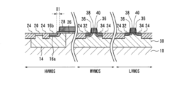
本実施の形態における半導体デバイス100では、図4に示すように、HVMOSのみならず、中耐圧電界効果トランジスタ(MVMOS:Middle Voltage Metal Oxide Semiconductor)及び低耐圧電界効果トランジスタ(LVMOS:Low Voltage Metal Oxide Semiconductor)が同じ半導体基板10に形成されている。なお、図4では、HVMOSについて本願において重要である拡張ソース領域16a及びソース領域16b側の構造のみを示している。
In the
MVMOS及びLVMOSは、N型の半導体基板10の表面領域に形成されたP型のウェル領域30、ウェル領域30内に形成された高濃度N型のソース領域32及びドレイン領域34、ソース領域32及びドレイン領域34から拡がり、ソース領域32及びドレイン領域34より低濃度のN型の拡張領域36、ソース領域32からドレイン領域34に跨がって形成されたゲート絶縁層38、ゲート絶縁層38上に形成されたポリシリコン等のゲート電極40から構成される。MVMOS及びLVMOSは、絶縁領域24によって半導体基板10上の他の素子から絶縁される。
MVMOS and LVMOS are composed of a P-
一般的に半導体デバイス100において、HVMOSは動作電圧範囲が25V~40V程度であり、MVMOSは動作電圧範囲が5V~7V程度であり、LVMOSは動作電圧範囲が1.2V~1.5V程度である。このような動作電圧範囲では、例えば、MVMOSのゲート絶縁層38の厚さは10nm~20nm程度とされ、LVMOSのゲート絶縁層38の厚さは4nm以下とされる。ただし、半導体デバイス100におけるHVMOS、MVMOS及びLVMOSの動作電圧範囲やゲート絶縁層38の厚さはこれらに限定されるものではない。すなわち、半導体デバイス100において、MVMOSの動作電圧範囲がHVMOSの動作電圧範囲より小さければよく、LVMOSの動作電圧範囲がMVMOSの動作電圧範囲がより小さければよい。また、半導体デバイス100において、MVMOSのゲート絶縁層38の厚さがHVMOSのゲート絶縁層26の厚さより薄ければよく、LVMOSのゲート絶縁層38の厚さがMVMOSのゲート絶縁層38の厚さより薄ければよい。
Generally, in the
また、半導体デバイス100では、LVMOSのゲート長が100nm以下であることが好適である。
Also, in the
MVMOSに拡張領域36を設けることによって、MVMOSのドレイン領域34の電界を緩和することができる。同様に、LVMOSに拡張領域36を設けることによって、LVMOSのドレイン領域34の電界を緩和することができる。
By providing the
[製造方法]
図5及び図6は、半導体デバイス100の製造方法を示す。図5及び図6は半導体デバイス100の製造方法を示す断面模式図であり、半導体デバイス100を構成する各部を強調して示しており、各部の平面方向の寸法及び厚さ方向の寸法は実際の比を示していない場合がある。
[Production method]
5 and 6 show a method of manufacturing the
以下、n型チャネルのHVMOS、MVMOS及びLVMOSを含む半導体デバイス100の製造方法について説明する。半導体基板10は、第1導電型としてp型にドーピングされたシリコン基板として説明する。なお、p型チャネルのHVMOSを含む半導体デバイス100とする場合、第1導電型をn型、第2導電型をp型として読み替えればよい。
A method of manufacturing a
ステップS10では、ドリフト領域12及びガードリング領域14が形成される。ドリフト領域12及びガードリング領域14は、ドーパントのイオン注入処理及びアニールによる拡散処理によって形成される。
At step S10, the
半導体基板10の表面においてドリフト領域12に対応する領域が開口領域であるマスクとして機能するレジスト層を形成する。レジスト層は、フォトリソグラフィ技術を用いてパターニングすることができる。第2導電型がn型である場合、レジスト層をマスクとして、n型ドーパント(燐P又は砒素As)を半導体基板10の表面にイオン注入する。ここでは、浅い領域へのイオン注入と、当該浅い領域へのイオン注入よりも高い注入エネルギーを用いたより深い領域へのイオン注入とを組み合わせた2段階注入を行うことが好適である。例えば、浅い領域へのイオン注入では、燐Pを200keV以上300keV以下のイオン注入エネルギーで1×10¹²以上2×10¹²/cm2以下の密度となるようにイオン注入する。また、より深い領域へのイオン注入では、600keV以上700keV以下のイオン注入エネルギーで4×1012以上6×1012/cm2以下の密度となるようにイオン注入する。ただし、イオン注入されるドーパントの密度、注入深さ等はHVMOSのサイズや特性に応じて適宜設定すればよい。イオン注入後、レジスト層は除去する。
A resist layer functioning as a mask is formed on the surface of the
また、ガードリング領域14へのドーパントのイオン注入処理が行われる。半導体基板10においてガードリング領域14に対応する領域が開口領域となるようにレジスト層を形成する。レジスト層は、フォトリソグラフィ技術を用いてパターニングすることができる。第1導電型がp型である場合、レジスト層をマスクとして、p型ドーパント(ボロンB又は二フッ化ボロンBF2)を半導体基板10の表面にイオン注入する。ここでは、浅い領域へのイオン注入と、当該浅い領域へのイオン注入よりも高い注入エネルギーを用いたより深い領域へのイオン注入とを組み合わせた2段階注入を行うことが好適である。例えば、浅い領域へのイオン注入では、ボロンBを100keV以上150keV以下のイオン注入エネルギーで1×10¹²以上2×10¹²/cm2以下の密度となるようにイオン注入する。また、より深い領域へのイオン注入では、300keV以上400keV以下のイオン注入エネルギーで1×1013以上2×1013/cm2以下の密度となるようにイオン注入する。ただし、イオン注入されるドーパントの密度、注入深さ等はHVMOSのサイズや特性に応じて適宜設定すればよい。イオン注入後、レジスト層は除去する。
Also, dopant ion implantation into the
その後、イオン拡散処理が行われる。ドリフト領域12及びガードリング領域14へドーパントを注入した後、半導体基板10を900℃~1300℃程度の高温でアニール(加熱)することによって半導体基板10内にドーパントを拡散させる。例えば、1100℃で5時間~7時間のアニール処理を行う。ただし、加熱温度及び時間は、HVMOSのサイズや特性に応じて適宜設定すればよい。第2導電型のドーパントが拡散した領域はドリフト領域12となり、第1導電型のドーパントが拡散した領域はガードリング領域14となる。
After that, an ion diffusion process is performed. After implanting the dopant into the
ステップS12では、絶縁領域22及び絶縁領域24が形成される。絶縁領域22及び絶縁領域24は、マスクを利用した既存のLOCOSプロセス又はSTIプロセスによって形成することができる。LOCOSプロセスでは、シリコン酸化膜(SiO2)やシリコン窒化膜(SiN)をマスクとして、酸素(O2)を供給しつつ半導体基板10を加熱することによって半導体基板10の表面においてマスクの開口領域を熱酸化することによって絶縁領域22又は絶縁領域24を形成することができる。また、STIプロセスでは、開口領域をトレンチエッチングし、その溝内に高密度プラズマCVD等を用いて絶縁膜を埋め込んだ後、当該領域を化学機械研磨法(CMP)で平坦化することで絶縁領域22又は絶縁領域24を形成することができる。
In step S12, insulating
ステップS14では、ゲート絶縁層26が形成される。ゲート絶縁層26は、テトラエトキシシラン(TEOS)を用いた化学気相成長法(CVD)により形成することができる。また、ゲート絶縁層26は、酸素(O2)等の酸素含有ガスや窒素(N2)等の窒素含有ガスを用いた熱酸化法により形成してもよい。レジストを用いたフォトリソグラフィ及びエッチングを適用して、半導体基板10の表面においてガードリング領域14及びドリフト領域12の一部並びに絶縁領域22の一部に跨がる領域にゲート絶縁層26が残るように形成される。HVMOSの動作電圧範囲を25V~40V程度とする場合、ゲート絶縁層26の膜厚は60nm以上100nm以下とすることが好適である。
In step S14, a
ステップS16では、MVMOS及びLVMOSにおけるウェル領域30並びにゲート絶縁層38が形成される。MVMOS及びLVMOSにおけるウェル領域30は、ドーパントのイオン注入処理及びアニールによる拡散処理によって形成される。
In step S16, well
半導体基板10の表面においてLVMOSのウェル領域30に対応する領域が開口領域であるマスクとして機能するレジスト層を形成する。レジスト層は、フォトリソグラフィ技術を用いてパターニングすることができる。レジスト層をマスクとして、p型ドーパント(ボロンB又は二フッ化ボロンBF2)を半導体基板10の表面にイオン注入する。イオン注入では、ボロンBを150keV以上250keV以下のイオン注入エネルギーで1.5×10¹³以上2.5×10¹³/cm2以下の密度となるようにイオン注入、ボロンBを80keV以上120keV以下のイオン注入エネルギーで4×1012以上1×1013/cm2以下の密度となるようにイオン注入、さらにボロンBを7keV以上20keV以下のイオン注入エネルギーで1×1013以上3×1013/cm2以下の密度となるようにイオン注入する。ただし、イオン注入されるドーパントの密度、注入深さ等はLVMOSのサイズや特性に応じて適宜設定すればよい。イオン注入後、レジスト層は除去する。
A resist layer functioning as a mask is formed on the surface of the
また、半導体基板10の表面においてMVMOSのウェル領域30に対応する領域が開口領域であるマスクとして機能するレジスト層を形成する。レジスト層は、フォトリソグラフィ技術を用いてパターニングすることができる。レジスト層をマスクとして、p型ドーパント(ボロンB又は二フッ化ボロンBF2)を半導体基板10の表面にイオン注入する。イオン注入では、ボロンBを150keV以上250keV以下のイオン注入エネルギーで1.5×10¹³以上2.5×10¹³/cm2以下の密度となるようにイオン注入、ボロンBを80keV以上120keV以下のイオン注入エネルギーで4×1012以上1×1013/cm2以下の密度となるようにイオン注入、さらにボロンBを20keV以上30keV以下のイオン注入エネルギーで1×1012以上3×1012/cm2以下の密度となるようにイオン注入する。ただし、イオン注入されるドーパントの密度、注入深さ等はMVMOSのサイズや特性に応じて適宜設定すればよい。イオン注入後、レジスト層は除去する。
Further, a resist layer functioning as a mask is formed on the surface of the
その後、イオン活性化処理が行われる。MVMOS及びLVMOSのウェル領域30へドーパントを注入した後、半導体基板10を900℃~1100℃程度の高温でアニール(加熱)することによって半導体基板10内のドーパントを活性化させる。例えば、1050℃で30秒~60秒のアニール処理を行う。ただし、加熱温度及び時間は、MVMOS及びLVMOSのサイズや特性に応じて適宜設定すればよい。第1導電型のドーパントが活性化した領域はMVMOS及びLVMOSのウェル領域30となる。
After that, an ion activation process is performed. After dopants are implanted into the
続いて、半導体基板10の表面においてMVMOS及びLVMOSのウェル領域30が形成された領域上にMVMOS及びLVMOSのゲート絶縁層38が形成される。ゲート絶縁層38は、酸素(O2)等の酸素含有ガスや窒素(N2)等の窒素含有ガスを用いた熱酸化法により形成することができる。レジストを用いたフォトリソグラフィ及びエッチングを適用して、半導体基板10の表面においてLVMOSのウェル領域30内に形成されたMVMOSのゲート絶縁層38を除去した後にLVMOSのゲート絶縁層38を形成する。MVMOSの動作電圧範囲を5V~7V程度とする場合、MVMOSのゲート絶縁層38の膜厚は10nm~20nm程度とすることが好適である。また、LVMOSの動作電圧範囲を1.2V~1.5V程度とする場合、LVMOSのゲート絶縁層38の厚さは4nm以下とすることが好適である。
Subsequently, the MVMOS and LVMOS
ステップS18では、HVMOSのゲート電極28並びにMVMOS及びLVMOSのゲート電極40が形成される。さらに、HVMOSの拡張ソース領域16a及びMVMOSの拡張領域36が形成される。
In step S18, the
HVMOSのゲート絶縁層26上にゲート電極28並びにMVMOS及びLVMOSのゲート絶縁層38上にゲート電極40が形成される。ゲート電極28及びゲート電極40の形成方法は、特に限定されるものではないが、多結晶シリコン層とする場合にはシラン(SiH4)等のシリコン含有ガスを用いた化学気相成長法(CVD法)とすることができる。ゲート電極28及びゲート電極40を金属層とする場合、蒸着法、スパッタリング法、化学気相成長法(CVD法)等を適用することができる。レジストを用いたフォトリソグラフィ及びエッチングを適用して、HVMOSのゲート電極28並びにMVMOS及びLVMOSのゲート電極40が必要な領域に形成される。このとき、ゲート絶縁層26の領域は、ゲート電極28の領域よりマージン距離X1(=0.1μm~0.2μm程度の重ねマージン分)だけ広くされる。
A
次に、HVMOSの拡張ソース領域16a及びMVMOSの拡張領域36のためのイオン注入処理が行われる。図5に示すように、HVMOSの拡張ソース領域16a及びMVMOSが形成される領域以外の領域にマスクとして機能するレジスト層Rを形成する。レジスト層Rは、フォトリソグラフィ技術を用いてパターニングすることができる。そして、第2導電型がn型である場合、レジスト層Rをマスクとして、n型ドーパント(燐P又は砒素As)を半導体基板10の表面にイオン注入する。ここでは、燐Pを60keV以上100keV以下のイオン注入エネルギーで1×10¹³以上3×10¹³/cm2以下の密度となるようにイオン注入する。ただし、イオン注入されるドーパントの密度、注入深さ等はHVMOSの拡張ソース領域16a及びMVMOSの拡張領域36として必要な特性に応じて適宜設定すればよい。イオン注入後、レジスト層Rは除去する。
An ion implantation process for the HVMOS
その後、イオン活性化処理が行われる。HVMOSの拡張ソース領域16a及びMVMOSの拡張領域36へドーパントを注入した後、半導体基板10を900℃~1050℃程度の高温でアニール(加熱)することによって半導体基板10内のドーパントを活性化させる。例えば、10秒~30秒のアニール処理を行う。ただし、加熱温度及び時間は、HVMOSの拡張ソース領域16a及びMVMOSの拡張領域36として必要な特性に応じて適宜設定すればよい。ドーパントが活性化した領域はHVMOSの拡張ソース領域16a及びMVMOSの拡張領域36となる。
After that, an ion activation process is performed. After implanting the dopant into the HVMOS
ここで、MVMOSの拡張領域36に対するドーパントのイオン注入エネルギーを適切に設定することによって、ゲート電極28が重畳されていないゲート絶縁層26のマージン距離X1下の半導体基板10内にも同時にドーパントをイオン注入することができる。例えば、MVMOSの拡張領域36に対するドーパントのイオン注入エネルギーを60keV以上100keVとすることで、60nm~100nmの膜厚を有するゲート絶縁層26を通して半導体基板10にドーパントをイオン注入することができる。そして、イオン活性化処理を施すことによって、MVMOSの拡張領域36を形成すると同時に、距離X1を超えてゲート電極28下のチャネル領域Cに到達するHVMOSの拡張ソース領域16aをガードリング領域14内に形成することができる。これにより、半導体デバイス100の製造工程数を少なくすることができる。また、ゲート電極28の端部に対してHVMOSの拡張ソース領域16aが自己整合(セルフアライメント)で形成されるので、ゲート長さの変化に対してHVMOSの拡張ソース領域16aの配置の精度を高めることができる。
Here, by appropriately setting the dopant ion implantation energy for the
なお、HVMOSの拡張ソース領域16aとMVMOSの拡張領域36とはその機能が異なる。すなわち、HVMOSの拡張ソース領域16aは、ソース領域16bとHVMOSのチャネル領域Cとを繋ぐ領域として機能する。したがって、HVMOSの拡張ソース領域16aを設けることによって、非対称HVMOSの閾値電圧Vthのばらつきを抑制することができる。一方、MVMOSの拡張領域36は、MVMOSのドレイン領域34の電界を緩和する領域として機能する。
The
ステップS20では、LVMOSの拡張領域36が形成される。LVMOSの拡張領域36が形成される領域以外の領域にマスクとして機能するレジスト層を形成する。レジスト層は、フォトリソグラフィ技術を用いてパターニングすることができる。そして、第2導電型がn型である場合、レジスト層をマスクとして、n型ドーパント(燐P又は砒素As)を半導体基板10の表面にイオン注入する。ここでは、砒素Asを2keV以上4keV以下のイオン注入エネルギーで6×10¹⁴以上2×10¹⁵/cm2以下の密度となるようにイオン注入する。ただし、イオン注入されるドーパントの密度、注入深さ等はLVMOSの拡張領域36として必要な特性に応じて適宜設定すればよい。イオン注入後、レジスト層は除去する。
In step S20, the
その後、イオン活性化処理が行われる。LVMOSの拡張領域36へドーパントを注入した後、半導体基板10を1000℃~1050℃程度の高温でスパイクアニール(加熱)することによって半導体基板10内のドーパントを活性化させる。ただし、加熱温度及び時間は、LVMOSの拡張領域36として必要な特性に応じて適宜設定すればよい。ドーパントが活性化した領域はLVMOSの拡張領域36となる。
After that, an ion activation process is performed. After implanting the dopant into the
ステップS22では、HVMOSのゲート電極28並びにMVMOS及びLVMOSのゲート電極40の側面に絶縁体からなるサイドウォールSが形成される。サイドウォールSは、テトラエトキシシラン(TEOS)を用いた化学気相成長法(CVD)により形成することができる。また、サイドウォールSは、酸素(O2)等の酸素含有ガスや窒素(N2)等の窒素含有ガスを用いた化学気相成長法(CVD)により形成してもよい。エッチングを適用して、HVMOSのゲート電極28並びにMVMOS及びLVMOSのゲート電極40の側面にサイドウォールSが残るように形成される。
In step S22, sidewalls S made of an insulator are formed on the side surfaces of the
ステップS24では、HVMOSのソース領域16b及びドレイン領域18並びにMVMOS及びLVMOSのソース領域32及びドレイン領域34が形成される。HVMOSのソース領域16b及びドレイン領域18並びにMVMOS及びLVMOSのソース領域32及びドレイン領域34は、ドーパントのイオン注入処理及びアニールによる拡散処理によって形成される。
In step S24,
半導体基板10の表面においてHVMOSのソース領域16b及びドレイン領域18並びにMVMOS及びLVMOSのソース領域32及びドレイン領域34に対応する領域が開口領域であるマスクとして機能するレジスト層を形成する。レジスト層は、フォトリソグラフィ技術を用いてパターニングすることができる。レジスト層をマスクとして、そして、第2導電型がn型である場合、レジスト層をマスクとして、n型ドーパント(燐P又は砒素As)を半導体基板10の表面にイオン注入する。ここでは、砒素Asを20keV以上25keV以下のイオン注入エネルギーで2×10¹⁵/cm2以上5×1015/cm2以下の密度となるようにイオン注入する。さらに、燐Pを20keV以上30keV以下のイオン注入エネルギーで3×1013以上1×1014/cm2以下の密度となるようにイオン注入する。ただし、イオン注入されるドーパントの密度、注入深さ等はHVMOSのソース領域16b及びドレイン領域18並びにMVMOS及びLVMOSのソース領域32及びドレイン領域34として必要な特性に応じて適宜設定すればよい。イオン注入後、レジスト層は除去する。
A resist layer functioning as a mask is formed on the surface of the
このように、HVMOSのソース領域16b及びドレイン領域18並びにMVMOS及びLVMOSのソース領域32及びドレイン領域34に対してドーパントのイオン注入を同時に行うことで半導体デバイス100の製造工程数を少なくすることができる。
In this way, the number of manufacturing steps of the
ステップS26では、HVMOSのタップ領域20が形成される。HVMOSのタップ領域20は、ドーパントのイオン注入処理及びアニールによる拡散処理によって形成される。
In step S26, the
半導体基板10の表面においてHVMOSのタップ領域20に対応する領域が開口領域であるマスクとして機能するレジスト層を形成する。レジスト層は、フォトリソグラフィ技術を用いてパターニングすることができる。レジスト層をマスクとして、p型ドーパント(ボロンB又は二フッ化ボロンBF2)を半導体基板10の表面にイオン注入する。イオン注入では、二フッ化ボロンBF2を5keV以上10keV以下のイオン注入エネルギーで2×10¹⁵以上3×10¹⁵/cm2以下の密度となるようにイオン注入する。さらに、例えば、ボロンBを5keV以上10keV以下のイオン注入エネルギーで2×1013以上5×1013/cm2以下の密度となるようにイオン注入する。ただし、イオン注入されるドーパントの密度、注入深さ等はHVMOSのサイズや特性に応じて適宜設定すればよい。イオン注入後、レジスト層は除去する。
A resist layer functioning as a mask is formed on the surface of the
その後、イオン活性化処理が行われる。HVMOSのタップ領域20へドーパントを注入した後、半導体基板10を1000℃~1050℃程度の高温でスパイクアニール(加熱)することによって半導体基板10内のドーパントを活性化させる。ドーパントが活性化した領域はHVMOSのソース領域16b及びドレイン領域18並びにMVMOS及びLVMOSのソース領域32及びドレイン領域34並びにHVMOSのタップ領域20となる。
After that, an ion activation process is performed. After implanting the dopant into the
[変形例]
図7は、半導体デバイス100の変形例における半導体デバイス102の構成の断面模式図を示す。半導体デバイス102も、非対称構造のHVMOS、対象構造のMVMOS及びLVMOSを含んで構成される。
[Modification]
FIG. 7 shows a schematic cross-sectional view of the configuration of a
なお、図7では、半導体デバイス102のHVMOSにおいて重要である拡張ソース領域16a及びソース領域16b側の構造のみを示している。また、図7は半導体デバイス102の基本構成を説明するための模式図であり、半導体デバイス102を構成する各部を強調して示しており、各部の平面方向の寸法及び厚さ方向の寸法は実際の比を示していない場合がある。
7 shows only the structure of the
半導体デバイス102のHVMOSは、半導体基板10、ドリフト領域12、ガードリング領域14、拡張ソース領域16a、ソース領域16b、ドレイン領域18、タップ領域20、絶縁領域22、絶縁領域24、ゲート絶縁層26及びゲート電極28を含んで構成される。
HVMOS of
半導体デバイス102は、半導体デバイス100と拡張ソース領域16aが異なっている。拡張ソース領域16aは、HVMOSのソースの一部を構成する領域である。拡張ソース領域16aは、ドリフト領域12と同じ導電型、すなわち第2導電型とする。拡張ソース領域16aのドーパント濃度は、1×10¹⁷/cm3以上1×1018/cm3以下とすることが好適である。拡張ソース領域16aは、ガードリング領域14内において絶縁領域24の領域下からゲート絶縁層26及びゲート電極28に重畳した領域まで延設される。すなわち、拡張ソース領域16aは、ゲート電極28下のチャネル領域Cに至るまで延設される。
また、半導体デバイス102では、HVMOSのみならず、中耐圧電界効果トランジスタ(MVMOS:Middle Voltage Metal Oxide Semiconductor)及び低耐圧電界効果トランジスタ(LVMOS:Low Voltage Metal Oxide Semiconductor)が同じ半導体基板10に形成されている。
Further, in the
半導体デバイス102のMVMOSでは、P型の半導体基板10にN型のウェル領域30bが形成され、当該N型のウェル領域30b内に高濃度P型のソース領域32b及びドレイン領域34b、ソース領域32b及びドレイン領域34bから拡がったソース領域32b及びドレイン領域34bより低濃度のP型の拡張領域36b、ソース領域32bからドレイン領域34bに跨がって形成されたゲート絶縁層38、ゲート絶縁層38上に形成されたポリシリコン等のゲート電極40から構成される。
In the MVMOS of the
[製造方法]
図8及び図9は、半導体デバイス102の製造方法を示す。図8及び図9は半導体デバイス102の製造方法を示す断面模式図であり、半導体デバイス102を構成する各部を強調して示しており、各部の平面方向の寸法及び厚さ方向の寸法は実際の比を示していない場合がある。
[Production method]
8 and 9 show a method of manufacturing the
半導体基板10は、第1導電型としてp型にドーピングされたシリコン基板として説明する。なお、p型チャネルのHVMOSを含む半導体デバイス102とする場合、第1導電型をn型、第2導電型をp型として読み替えればよい。
The
ステップS30では、ドリフト領域12及びガードリング領域14が形成される。ドリフト領域12及びガードリング領域14は、ドーパントのイオン注入処理及びアニールによる拡散処理によって形成される。当該ステップにおける処理は、半導体デバイス100の製造方法におけるステップS10と同様であるので説明を省略する。
At step S30, the
ステップS32では、絶縁領域22及び絶縁領域24が形成される。当該ステップにおける処理は、半導体デバイス100の製造方法におけるステップS12と同様であるので説明を省略する。
In step S32, insulating
ステップS34では、ゲート絶縁層26が形成される。当該ステップにおける処理は、半導体デバイス100の製造方法におけるステップS14と同様であるので説明を省略する。
In step S34, the
ステップS36では、LVMOSにおけるウェル領域30が形成される。また、MVMOSのウェル領域30b及びHVMOSの拡張ソース領域16aへのイオン注入処理が行われる。
In step S36, well
半導体基板10の表面においてLVMOSのウェル領域30に対応する領域が開口領域であるマスクとして機能するレジスト層を形成する。レジスト層は、フォトリソグラフィ技術を用いてパターニングすることができる。レジスト層をマスクとして、p型ドーパント(ボロンB又は二フッ化ボロンBF2)を半導体基板10の表面にイオン注入する。イオン注入では、ボロンBを150keV以上250keV以下のイオン注入エネルギーで1.5×10¹³以上2.5×10¹³/cm2以下の密度となるようにイオン注入、ボロンBを80keV以上120keV以下のイオン注入エネルギーで4×1012以上1×1013/cm2以下の密度となるようにイオン注入、さらにボロンBを7keV以上20keV以下のイオン注入エネルギーで1×1013以上3×1013/cm2以下の密度となるようにイオン注入する。ただし、イオン注入されるドーパントの密度、注入深さ等はLVMOSのサイズや特性に応じて適宜設定すればよい。イオン注入後、レジスト層は除去する。
A resist layer functioning as a mask is formed on the surface of the
半導体基板10の表面においてMVMOSのウェル領域30b及びHVMOSの拡張ソース領域16aに対応する領域が開口領域であるマスクとして機能するレジスト層Rを形成する。レジスト層Rは、フォトリソグラフィ技術を用いてパターニングすることができる。ここで、レジスト層Rは、後述するゲート絶縁層26のマージン距離X1となる領域も開口部となるように形成される。レジスト層Rをマスクとして、n型ドーパント(燐P又は砒素As)を半導体基板10の表面にイオン注入する。イオン注入では、燐Pを400keV以上600keV以下のイオン注入エネルギーで1.5×10¹³以上2.5×10¹³/cm2以下の密度となるようにイオン注入、燐Pを200keV以上300keV以下のイオン注入エネルギーで5×1012以上1×1013/cm2以下の密度となるようにイオン注入、さらに燐Pを60keV以上80keV以下のイオン注入エネルギーで1×1012以上3×1012/cm2以下の密度となるようにイオン注入する。ただし、イオン注入されるドーパントの密度、注入深さ等はMVMOSのウェル領域30b及びHVMOSの拡張ソース領域16aとして必要な特性に応じて適宜設定すればよい。イオン注入後、レジスト層Rは除去する。
A resist layer R functioning as a mask is formed on the surface of the
その後、イオン活性化処理が行われる。LVMOSのウェル領域30並びにMVMOSのウェル領域30b及びHVMOSの拡張ソース領域16aへドーパントを注入した後、半導体基板10を900℃~1100℃程度の高温でアニール(加熱)することによって半導体基板10内のドーパントを活性化させる。例えば、1050℃で30秒~60秒のアニール処理を行う。ただし、加熱温度及び時間は、MVMOS及びLVMOSのサイズや特性に応じて適宜設定すればよい。これによって、LVMOSのウェル領域30並びにMVMOSのウェル領域30b及びHVMOSの拡張ソース領域16aが形成される。
After that, an ion activation process is performed. After dopants are implanted into the
ここで、一般的にMVMOSのウェル領域30bに対するドーパントのイオン注入エネルギーでは60nm~100nmの厚さのゲート絶縁層26を容易に透過するので、ゲート絶縁層26のマージン距離X1下の半導体基板10内にも同時にドーパントをイオン注入することができる。そして、イオン活性化処理を施すことによって、MVMOSのウェル領域30bを形成すると同時に、距離X1を超えてゲート電極28下のチャネル領域Cに到達するHVMOSの拡張ソース領域16aをガードリング領域14内に形成することができる。これにより、半導体デバイス102の製造工程数を少なくすることができる。
Here, in general, the ion implantation energy of the dopant into the
ステップS38では、MVMOS及びLVMOSのゲート絶縁層38が形成される。さらに、HVMOSのゲート電極28並びにMVMOS及びLVMOSのゲート電極40が形成される。
In step S38,
半導体基板10の表面においてMVMOSのウェル領域30b及びLVMOSのウェル領域30が形成された領域上にMVMOS及びLVMOSのゲート絶縁層38が形成される。ゲート絶縁層38は、酸素(O2)等の酸素含有ガスや窒素(N2)等の窒素含有ガスを用いた熱酸化法により形成することができる。フォトエッチングプロセスを使用することにより、半導体基板10の表面上にLVMOSのゲート絶縁層38及びMVMOSのゲート絶縁層38を形成する。LVMOSのゲート絶縁層38は、LVMOSのウェル領域30上に配置される。MVMOSのゲート絶縁層38は、MVMOSのウェル領域30b上に配置される。例えば、半導体基板10の表面のパッド酸化物層を最初に除去し、パターン化されたフォトレジスト層をマスクとして使用して熱酸化によってMVMOSのウェル領域30b上にMVMOSのゲート絶縁層38を形成し、フォトレジスト層を除去する。その後、別のパターン化されたフォトレジスト層をマスクとして使用して、熱酸化によってLVMOSのウェル領域30上にLVMOSのゲート絶縁層38を形成する。MVMOSの動作電圧範囲を5V~7V程度とする場合、MVMOSのゲート絶縁層38の膜厚は10nm~20nm程度とすることが好適である。また、LVMOSの動作電圧範囲を1.2V~1.5V程度とする場合、LVMOSのゲート絶縁層38の厚さは4nm以下とすることが好適である。
MVMOS and LVMOS
また、HVMOSのゲート電極28並びにMVMOS及びLVMOSのゲート電極40が形成される。HVMOSのゲート絶縁層26上にゲート電極28並びにMVMOS及びLVMOSのゲート絶縁層38上にゲート電極40が形成される。ゲート電極28及びゲート電極40の形成方法は、特に限定されるものではないが、多結晶シリコン層とする場合にはシラン(SiH4)等のシリコン含有ガスを用いた化学気相成長法(CVD法)とすることができる。ゲート電極28及びゲート電極40を金属層とする場合、蒸着法、スパッタリング法、化学気相成長法(CVD法)等を適用することができる。レジストを用いたフォトリソグラフィ及びエッチングを適用して、HVMOSのゲート電極28並びにMVMOS及びLVMOSのゲート電極40が必要な領域に形成される。このとき、ゲート絶縁層26の領域は、ゲート電極28の領域よりマージン距離X1(=0.1μm~0.2μm程度の重ねマージン分)だけ広くされる。
Also, a
ステップS40では、MVMOSの拡張領域36b及びLVMOSの拡張領域36が形成される。
In step S40, the
MVMOSの拡張領域36bのためのイオン注入処理が行われる。MVMOSの拡張領域36bが形成される領域以外の領域にマスクとして機能するレジスト層を形成する。レジスト層は、フォトリソグラフィ技術を用いてパターニングすることができる。そして、レジスト層をマスクとして、p型ドーパント(ボロンB又は二フッ化ボロンBF2)を半導体基板10の表面にイオン注入する。イオン注入では、ボロンBを15keV以上25keV以下のイオン注入エネルギーで1×10¹³以上3×10¹³/cm2以下の密度となるようにイオン注入する。ただし、イオン注入されるドーパントの密度、注入深さ等はMVMOSの拡張領域36bとして必要な特性に応じて適宜設定すればよい。イオン注入後、レジスト層は除去する。
An ion implantation process for the
また、LVMOSの拡張領域36のためのイオン注入処理が行われる。LVMOSの拡張領域36が形成される領域以外の領域にマスクとして機能するレジスト層を形成する。レジスト層は、フォトリソグラフィ技術を用いてパターニングすることができる。そして、レジスト層をマスクとして、n型ドーパント(燐P又は砒素As)を半導体基板10の表面にイオン注入する。ここでは、砒素Asを2keV以上4keV以下のイオン注入エネルギーで6×10¹⁴以上2×10¹⁵/cm2以下の密度となるようにイオン注入する。ただし、イオン注入されるドーパントの密度、注入深さ等はLVMOSの拡張領域36として必要な特性に応じて適宜設定すればよい。イオン注入後、レジスト層は除去する。
An ion implantation process for the
その後、イオン活性化処理が行われる。MVMOSの拡張領域36b及びLVMOSの拡張領域36へドーパントを注入した後、半導体基板10を1000℃~1050℃程度の高温でスパイクアニール(加熱)することによって半導体基板10内のドーパントを活性化させる。ただし、加熱温度及び時間は、MVMOSの拡張領域36b及びLVMOSの拡張領域36として必要な特性に応じて適宜設定すればよい。ドーパントが活性化した領域はMVMOSの拡張領域36b及びLVMOSの拡張領域36となる。
After that, an ion activation process is performed. After implanting the dopant into the
ステップS42では、HVMOSのゲート電極28並びにMVMOS及びLVMOSのゲート電極40の側面に絶縁体からなるサイドウォールSが形成される。当該ステップにおける処理は、半導体デバイス100の製造方法におけるステップS22と同様であるので説明を省略する。
In step S42, sidewalls S made of an insulator are formed on the side surfaces of the
ステップS44では、HVMOSのソース領域16b及びドレイン領域18並びにLVMOSのソース領域32及びドレイン領域34を形成するためのイオン注入処理が行われる。
In step S44, an ion implantation process is performed to form the
半導体基板10の表面においてHVMOSのソース領域16b及びドレイン領域18並びにLVMOSのソース領域32及びドレイン領域34に対応する領域が開口領域であるマスクとして機能するレジスト層Rを形成する(図9のステップS44参照)。レジスト層Rは、フォトリソグラフィ技術を用いてパターニングすることができる。そして、レジスト層Rをマスクとして、n型ドーパント(燐P又は砒素As)を半導体基板10の表面にイオン注入する。ここでは、砒素Asを20keV以上25keV以下のイオン注入エネルギーで2×10¹⁵/cm2以上5×1015/cm2以下の密度となるようにイオン注入する。さらに、燐Pを20keV以上30keV以下のイオン注入エネルギーで3×1013以上1×1014/cm2以下の密度となるようにイオン注入する。ただし、イオン注入されるドーパントの密度、注入深さ等はHVMOSのソース領域16b及びドレイン領域18並びにLVMOSのソース領域32及びドレイン領域34として必要な特性に応じて適宜設定すればよい。イオン注入後、レジスト層Rは除去する。
On the surface of the
ステップS46では、HVMOSのタップ領域20並びにMVMOSのソース領域32b及びドレイン領域34bを形成するためのイオン注入処理が行われる。
In step S46, an ion implantation process is performed to form the
半導体基板10の表面においてHVMOSのタップ領域20並びにMVMOSのソース領域32b及びドレイン領域34bに対応する領域が開口領域であるマスクとして機能するレジスト層を形成する。レジスト層は、フォトリソグラフィ技術を用いてパターニングすることができる。そして、レジスト層をマスクとして、p型ドーパント(ボロンB又は二フッ化ボロンBF2)を半導体基板10の表面にイオン注入する。ここでは、イオン注入では、二フッ化ボロンBF2を5keV以上10keV以下のイオン注入エネルギーで2×10¹⁵以上3×10¹⁵/cm2以下の密度となるようにイオン注入する。さらに、例えば、ボロンBを5keV以上10keV以下のイオン注入エネルギーで2×1013以上5×1013/cm2以下の密度となるようにイオン注入する。ただし、イオン注入されるドーパントの密度、注入深さ等はHVMOSのタップ領域20並びにMVMOSのソース領域32b及びドレイン領域34bとして必要な特性に応じて適宜設定すればよい。イオン注入後、レジスト層は除去する。
A resist layer functioning as a mask is formed on the surface of the
その後、イオン活性化処理が行われる。HVMOSのソース領域16b及びドレイン領域18並びにLVMOSのソース領域32及びドレイン領域34並びにHVMOSのタップ領域20並びにMVMOSのソース領域32b及びドレイン領域34bへドーパントを注入した後、半導体基板10を1000℃~1050℃程度の高温でスパイクアニール(加熱)することによって半導体基板10内のドーパントを活性化させる。ただし、加熱温度及び時間は、HVMOSのソース領域16b及びドレイン領域18並びにLVMOSのソース領域32及びドレイン領域34並びにHVMOSのタップ領域20並びにMVMOSのソース領域32b及びドレイン領域34bとして必要な特性に応じて適宜設定すればよい。ドーパントが活性化した領域はHVMOSのソース領域16b及びドレイン領域18並びにLVMOSのソース領域32及びドレイン領域34並びにHVMOSのタップ領域20並びにMVMOSのソース領域32b及びドレイン領域34bとなる。
After that, an ion activation process is performed. After dopant implantation into
[本実施の形態における半導体デバイスの特性]
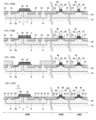
図10及び図11は、従来の非対称HVMOSの構造及び本実施の形態における半導体デバイス100の構造とした場合のソース領域近傍のドーパントの2次元濃度プロファイルをTCADシミュレーションした結果を示す。当該シミュレーションは、LVMOSのゲート長が100nm以下となり、LVMOSのソース領域32及びドレイン領域34のイオン注入エネルギーが小さくされた場合について想定したものである。図10(a)は、従来の非対称HVMOSの構造においてゲート絶縁層26の厚さを77nmとした場合のドーパントの2次元濃度プロファイルを示す。また、図10(b)は、本実施の形態における半導体デバイス100の構造においてゲート絶縁層26の厚さを77nmとした場合の2次元濃度プロファイルを示す。図11(a)は、従来の非対称HVMOSの構造においてゲート絶縁層26の厚さを87nmとした場合のドーパントの2次元濃度プロファイルを示す。また、図11(b)は、本実施の形態における半導体デバイス100の構造においてゲート絶縁層26の厚さを87nmとした場合の2次元濃度プロファイルを示す。
[Characteristics of semiconductor device in the present embodiment]
10 and 11 show the results of TCAD simulation of two-dimensional dopant concentration profiles in the vicinity of the source region in the case of the conventional asymmetric HVMOS structure and the structure of the
図10(a)及び図11(a)に示されるように、ゲート絶縁層26の厚さが77nm及び87nmのいずれにおいても、従来の非対称HVMOSの構造の場合にはソース領域におけるドーパントの拡がりが十分でなく、ゲート電極28に対するゲート絶縁層26の幅のマージン距離X1を超えてゲート電極28下のチャネル領域Cまでドーパントが拡がらなかった。一方、図10(b)及び図11(b)に示されるように、ゲート絶縁層26の厚さが77nm及び87nmのいずれにおいても、拡張ソース領域16aを設けた本実施の形態における半導体デバイス100の構造の場合には拡張ソース領域16a及びソース領域16bにおける電界の拡がりが大きくなり、ゲート電極28に対するゲート絶縁層26の幅のマージン距離X1を超えてゲート電極28下のチャネル領域Cまで十分にドーパントが拡がった。
As shown in FIGS. 10(a) and 11(a), for both 77 nm and 87 nm thicknesses of the
図12は、従来の非対称HVMOSの構造及び本実施の形態における半導体デバイス100の構造とした場合のゲート-ソース電圧(Vgs)とドレイン-ソース電流(Ids)との関係をTCADシミュレーションした結果を示す。図12(a)は、従来の非対称HVMOSの構造に対するゲート-ソース電圧(Vgs)とドレイン-ソース電流(Ids)との関係を示す。図12(b)は、半導体デバイス100の構造に対するゲート-ソース電圧(Vgs)とドレイン-ソース電流(Ids)との関係を示す。
FIG. 12 shows the results of TCAD simulation of the relationship between the gate-source voltage (Vgs) and the drain-source current (Ids) in the case of the conventional asymmetric HVMOS structure and the structure of the
従来の非対称HVMOSの構造では、ゲート絶縁層26の厚さを77nmから87nmへ増加させると、ゲート-ソース電圧(Vgs)とドレイン-ソース電流(Ids)との関係が大きく変動した。これに対して、本実施の形態における半導体デバイス100の構造では、ゲート絶縁層26の厚さを77nmから87nmへ増加させたとしてもゲート-ソース電圧(Vgs)とドレイン-ソース電流(Ids)との関係の変動は従来の非対称HVMOSの構造より小さくなった。
In a conventional asymmetric HVMOS structure, increasing the thickness of the
図13(a)及び図13(b)は、それぞれ従来の非対称HVMOSの構造及び本実施の形態の半導体デバイス100におけるゲート絶縁層26の膜厚と閾値電圧(Vth)とドレイン-ソース電流(Ids)との関係を示す。
13(a) and 13(b) show the film thickness, threshold voltage (Vth), and drain-source current (Ids) of the
図13(a)に示されるように、本実施の形態の半導体デバイス100におけるゲート絶縁層26の膜厚の変化に対する閾値電圧(Vth)の変化の幅は、従来の非対称HVMOSの構造における閾値電圧(Vth)の変化の幅より小さくなった。すなわち、本実施の形態の半導体デバイス100では、ゲート絶縁層26の膜厚に対して閾値電圧(Vth)を安定にすることができた。
As shown in FIG. 13A, the width of change in the threshold voltage (Vth) with respect to the change in the film thickness of the
また、図13(b)に示されるように、本実施の形態の半導体デバイス100におけるゲート絶縁層26の膜厚の変化に対するドレイン-ソース電流(Ids)の変化の幅は、従来の非対称HVMOSの構造におけるドレイン-ソース電流(Ids)の変化の幅より小さくなった。すなわち、本実施の形態の半導体デバイス100では、ゲート絶縁層26の膜厚に対してドレイン-ソース電流(Ids)を安定にすることができた。
Further, as shown in FIG. 13B, the width of change in the drain-source current (Ids) with respect to the change in the film thickness of the
なお、ゲート絶縁層26の膜厚に対してのみならず、マージン距離X1のばらつきに対しても閾値電圧(Vth)やソース-ドレイン電流(Ids)の素子毎のバラツキを抑制することができる。
It is possible to suppress variations in the threshold voltage (Vth) and the source-drain current (Ids) for each device not only for the film thickness of the
以上のように、本発明によれば、非対称構造のHVMOSを含む半導体デバイスの特性を向上させる。すなわち、非対称構造のHVMOSを含む半導体デバイスにおいて閾値電圧(Vth)やソース-ドレイン電流(Ids)の素子毎のバラツキを抑制し、デバイス性能を安定化させることができる。特に、LVMOSのゲート長が100nm以下であるような構成において有効である。また、そのような良好な特性を有する非対称構造のHVMOSとMVMOS及びLVMOSを含む半導体デバイスにおいて製造工程を簡素化することを可能とし、製造コストを低減させることができる。 As described above, according to the present invention, the characteristics of a semiconductor device including an asymmetrically structured HVMOS are improved. That is, in a semiconductor device including an HVMOS with an asymmetric structure, variations in threshold voltage (Vth) and source-drain current (Ids) between devices can be suppressed, and device performance can be stabilized. In particular, it is effective in a configuration in which the gate length of LVMOS is 100 nm or less. In addition, it is possible to simplify the manufacturing process of semiconductor devices including HVMOS, MVMOS, and LVMOS of asymmetric structures having such good characteristics, and to reduce the manufacturing cost.
10 半導体基板、12 ドリフト領域、14 ガードリング領域、16 ソース領域、16a 拡張ソース領域、16b ソース領域、18 ドレイン領域、20 タップ領域、22 絶縁領域、24 絶縁領域、26 ゲート絶縁層、28 ゲート電極、30 ウェル領域、30b ウェル領域、32 ソース領域、32b ソース領域、34 ドレイン領域、34b ドレイン領域、36 拡張領域、36b 拡張領域、38 ゲート絶縁層、40 ゲート電極、100,102 半導体デバイス。
10
Claims (15)
第1導電型の半導体の基板と、
前記基板内において前記第1導電型と反対の第2導電型であるソース領域及びドレイン領域と、
前記基板上に形成され、厚さが60nm以上であるゲート絶縁層と、
前記ゲート絶縁層上に形成されたゲート電極と、
前記ゲート絶縁層下に設けられたチャネル領域と、
前記ドレイン領域と前記チャネル領域との間に絶縁領域と、
を備え、
前記ドレイン領域は前記ソース領域より前記ゲート電極から離れた位置に配置され、前記ゲート電極に対して前記ソース領域と前記ドレイン領域が非対称とされている非対称電界効果トランジスタであり、
前記ゲート絶縁層は、前記ソース領域側において前記ゲート電極よりもマージン距離だけ拡げられた拡張絶縁領域を有し、
前記ソース領域から前記ゲート電極の間には前記拡張絶縁領域以外の絶縁領域を有さず、
前記ソース領域から前記ゲート絶縁層の前記拡張絶縁領域下を介して前記ゲート電極下の前記基板内の領域まで延設された前記第2導電型の拡張ソース領域を有し、
前記ソース領域は、前記拡張ソース領域内に形成されていることを特徴とする半導体デバイス。 A semiconductor device,
a semiconductor substrate of a first conductivity type;
source and drain regions of a second conductivity type opposite the first conductivity type in the substrate;
a gate insulating layer formed on the substrate and having a thickness of 60 nm or more;
a gate electrode formed on the gate insulating layer;
a channel region provided under the gate insulating layer;
an insulating region between the drain region and the channel region;
with
an asymmetric field effect transistor in which the drain region is located farther from the gate electrode than the source region, and the source region and the drain region are asymmetric with respect to the gate electrode;
the gate insulating layer has an extended insulating region that is wider than the gate electrode by a margin distance on the source region side;
having no insulating region other than the extended insulating region between the source region and the gate electrode;
an extended source region of the second conductivity type extending from the source region through the extended insulating region of the gate insulating layer to a region in the substrate under the gate electrode;
The semiconductor device of claim 1, wherein said source region is formed within said extended source region.
前記基板内において前記第2導電型であるドリフト領域が形成され、
前記ドレイン領域は、前記ドリフト領域内に配置され、
前記拡張ソース領域は、前記基板の表面から前記ドリフト領域よりも浅いことを特徴とする半導体デバイス。 A semiconductor device according to claim 1, wherein
forming a drift region of the second conductivity type in the substrate;
the drain region is disposed within the drift region;
The semiconductor device of claim 1, wherein the extended source region is shallower than the drift region from the surface of the substrate.
前記ゲート絶縁層と前記ゲート電極が重なり合った領域から前記ドレイン領域の前記ゲート電極側の端部又はその近傍に亘って前記基板内に形成された絶縁領域を有することを特徴とする半導体デバイス。 3. A semiconductor device according to claim 1 or 2,
1. A semiconductor device comprising an insulating region formed in said substrate from a region where said gate insulating layer and said gate electrode overlap to an end of said drain region on said gate electrode side or the vicinity thereof.
前記ゲート絶縁層の厚さは、100nm以下であることを特徴とする半導体デバイス。 A semiconductor device according to any one of claims 1 to 3,
A semiconductor device, wherein the gate insulating layer has a thickness of 100 nm or less.
前記拡張ソース領域は、前記基板内に形成された前記第1導電型のウェル領域内に形成されていることを特徴とする半導体デバイス。 A semiconductor device according to any one of claims 1 to 4,
A semiconductor device, wherein said extended source region is formed within said well region of said first conductivity type formed within said substrate.
前記非対称電界効果トランジスタの動作電圧は25V以上40V以下であることを特徴とする半導体デバイス。 A semiconductor device according to any one of claims 1 to 5,
A semiconductor device, wherein the operating voltage of said asymmetric field effect transistor is between 25V and 40V.
前記基板を共通として、前記非対称電界効果トランジスタの前記ゲート絶縁層の厚さより薄い第2のゲート絶縁層を有する電界効果トランジスタであって、当該電界効果トランジスタを構成する前記第2のゲート絶縁層に対して第2のソース領域及び第2のドレイン領域が対称となるように配置された対称電界効果トランジスタを含むことを特徴とする半導体デバイス。 A semiconductor device according to any one of claims 1 to 6,
A field effect transistor having the substrate in common and a second gate insulating layer thinner than the thickness of the gate insulating layer of the asymmetric field effect transistor, wherein the second gate insulating layer constituting the field effect transistor includes: A semiconductor device comprising a symmetrical field effect transistor having a second source region and a second drain region arranged symmetrically to each other.
前記対称電界効果トランジスタは、ゲート長が100nm以下であることを特徴とする半導体デバイス。 A semiconductor device according to claim 7, wherein
A semiconductor device, wherein the symmetric field effect transistor has a gate length of 100 nm or less.
前記対称電界効果トランジスタは、ゲート絶縁層の厚さが10nm以上20nm以下であることを特徴とする半導体デバイス。 A semiconductor device according to claim 7, wherein
A semiconductor device, wherein the symmetrical field effect transistor has a gate insulating layer with a thickness of 10 nm or more and 20 nm or less.
前記対称電界効果トランジスタとして、
ゲート長が100nm以下である第1の電界効果トランジスタと、
ゲート絶縁層の厚さが10nm以上20nm以下である第2の電界効果トランジスタと、
を含むことを特徴とする半導体デバイス。 A semiconductor device according to claim 7, wherein
As the symmetric field effect transistor,
a first field effect transistor having a gate length of 100 nm or less;
a second field effect transistor having a gate insulating layer with a thickness of 10 nm or more and 20 nm or less;
A semiconductor device comprising:
第1導電型の半導体の基板と、
前記基板内において前記第1導電型と反対の第2導電型である第1ソース領域及び第1ドレイン領域と、
前記基板上に形成され、厚さが60nm以上である第1ゲート絶縁層と、
前記第1ゲート絶縁層上に形成された第1ゲート電極と、
前記第1ゲート絶縁層下に設けられたチャネル領域と、
前記第1ドレイン領域と前記チャネル領域との間に絶縁領域と、
を備え、
前記第1ドレイン領域は前記第1ソース領域より前記第1ゲート電極から離れた位置に配置され、前記第1ゲート電極に対して前記第1ソース領域と前記第1ドレイン領域が非対称とされており、
前記第1ゲート絶縁層は、前記第1ソース領域側において前記第1ゲート電極よりもマージン距離だけ拡げられた拡張絶縁領域を有し、
前記第1ソース領域から前記第1ゲート電極の間には前記拡張絶縁領域以外の絶縁領域を有さず、
前記第1ソース領域から前記第1ゲート絶縁層の前記拡張絶縁領域下を介して前記第1ゲート電極下の前記基板内の領域まで延設された前記第2導電型の拡張ソース領域を有し、
前記第1ソース領域は、前記拡張ソース領域内に形成されている第1電界効果トランジスタと、
前記基板内において第2ソース領域及び第2ドレイン領域と、
前記基板上に形成された第2ゲート絶縁層と、
前記第2ゲート絶縁層上に形成された第2ゲート電極と、
を備え、
前記第2ゲート絶縁層は前記第1電界効果トランジスタの前記第1ゲート絶縁層の厚さより薄く、前記第1電界効果トランジスタよりも低い動作電圧を有する第2電界効果トランジスタと、
を含む半導体デバイスの製造方法であり、
前記拡張ソース領域と前記第2ソース領域の少なくとも一部を同一の製造工程にて形成することを特徴とする半導体デバイスの製造方法。 A method of manufacturing a semiconductor device, comprising:
a semiconductor substrate of a first conductivity type;
a first source region and a first drain region of a second conductivity type opposite the first conductivity type in the substrate;
a first gate insulating layer formed on the substrate and having a thickness of 60 nm or more;
a first gate electrode formed on the first gate insulating layer;
a channel region provided under the first gate insulating layer;
an insulating region between the first drain region and the channel region;
with
The first drain region is arranged at a position farther from the first gate electrode than the first source region, and the first source region and the first drain region are asymmetric with respect to the first gate electrode. ,
the first gate insulating layer has an extended insulating region extended by a margin distance from the first gate electrode on the first source region side;
having no insulating region other than the extended insulating region between the first source region and the first gate electrode;
an extended source region of the second conductivity type extending from the first source region through the extended insulating region of the first gate insulating layer to a region in the substrate under the first gate electrode; ,
a first field effect transistor, wherein the first source region is formed within the extended source region;
a second source region and a second drain region in the substrate;
a second gate insulating layer formed on the substrate;
a second gate electrode formed on the second gate insulating layer;
with
a second field effect transistor having a lower operating voltage than the first field effect transistor, wherein the second gate insulating layer is thinner than the thickness of the first gate insulating layer of the first field effect transistor;
A method of manufacturing a semiconductor device comprising
A method of manufacturing a semiconductor device, wherein at least part of the extended source region and the second source region are formed in the same manufacturing process.
第1導電型の半導体の基板と、
前記基板内において前記第1導電型と反対の第2導電型である第1ソース領域及び第1ドレイン領域と、
前記基板上に形成され、厚さが60nm以上である第1ゲート絶縁層と、
前記第1ゲート絶縁層上に形成された第1ゲート電極と、
前記第1ゲート絶縁層下に設けられたチャネル領域と、
前記第1ドレイン領域と前記チャネル領域との間に絶縁領域と、
を備え、
前記第1ドレイン領域は前記第1ソース領域より前記第1ゲート電極から離れた位置に配置され、前記第1ゲート電極に対して前記第1ソース領域と前記第1ドレイン領域が非対称とされており、
前記第1ゲート絶縁層は、前記第1ソース領域側において前記第1ゲート電極よりもマージン距離だけ拡げられた拡張絶縁領域を有し、
前記第1ソース領域から前記第1ゲート電極の間には前記拡張絶縁領域以外の絶縁領域を有さず、
前記第1ソース領域から前記第1ゲート絶縁層の前記拡張絶縁領域下を介して前記第1ゲート電極下の前記基板内の領域まで延設された前記第2導電型の拡張ソース領域を有し、
前記第1ソース領域は、前記拡張ソース領域内に形成されている第1電界効果トランジスタと、
前記基板内において前記第2導電型であるウェル領域と、
前記ウェル領域内において前記第1導電型の第2ソース領域及び第2ドレイン領域と、
前記基板上に形成された第2ゲート絶縁層と、
前記第2ゲート絶縁層上に形成された第2ゲート電極と、
を備え、
前記第2ゲート絶縁層は前記第1電界効果トランジスタの前記第1ゲート絶縁層の厚さより薄く、前記第1電界効果トランジスタよりも低い動作電圧を有する第2電界効果トランジスタと、
を含む半導体デバイスの製造方法であり、
前記拡張ソース領域と前記ウェル領域を同一の製造工程にて形成することを特徴とする半導体デバイスの製造方法。 A method of manufacturing a semiconductor device, comprising:
a semiconductor substrate of a first conductivity type;
a first source region and a first drain region of a second conductivity type opposite the first conductivity type in the substrate;
a first gate insulating layer formed on the substrate and having a thickness of 60 nm or more;
a first gate electrode formed on the first gate insulating layer;
a channel region provided under the first gate insulating layer;
an insulating region between the first drain region and the channel region;
with
The first drain region is arranged at a position farther from the first gate electrode than the first source region, and the first source region and the first drain region are asymmetric with respect to the first gate electrode. ,
the first gate insulating layer has an extended insulating region extended by a margin distance from the first gate electrode on the first source region side;
having no insulating region other than the extended insulating region between the first source region and the first gate electrode;
an extended source region of the second conductivity type extending from the first source region through the extended insulating region of the first gate insulating layer to a region in the substrate under the first gate electrode; ,
a first field effect transistor, wherein the first source region is formed within the extended source region;
a well region of the second conductivity type in the substrate;
a second source region and a second drain region of the first conductivity type in the well region;
a second gate insulating layer formed on the substrate;
a second gate electrode formed on the second gate insulating layer;
with
a second field effect transistor having a lower operating voltage than the first field effect transistor, wherein the second gate insulating layer is thinner than the thickness of the first gate insulating layer of the first field effect transistor;
A method of manufacturing a semiconductor device comprising
A method of manufacturing a semiconductor device, wherein the extended source region and the well region are formed in the same manufacturing process.
前記半導体デバイスは、さらに、
前記基板内において第3ソース領域及び第3ドレイン領域と、
前記基板上に形成された第3ゲート絶縁層と、
前記第3ゲート絶縁層上に形成された第3ゲート電極と、
を備え、前記第2電界効果トランジスタの前記第2ゲート絶縁層の厚さより薄い前記第3ゲート絶縁層を有し、前記第2電界効果トランジスタよりも低い動作電圧を有する第3電界効果トランジスタを含み、
前記第1ソース領域の少なくとも一部と前記第3ソース領域の少なくとも一部を同一の製造工程にて形成することを特徴とする半導体デバイスの製造方法。 A method for manufacturing a semiconductor device according to claim 11 or 12,
The semiconductor device further comprises:
a third source region and a third drain region in the substrate;
a third gate insulating layer formed on the substrate;
a third gate electrode formed on the third gate insulating layer;
and a third field effect transistor having a lower operating voltage than the second field effect transistor, the third gate insulating layer being thinner than the thickness of the second gate insulating layer of the second field effect transistor. ,
A method of manufacturing a semiconductor device, wherein at least part of the first source region and at least part of the third source region are formed in the same manufacturing process.
前記第3電界効果トランジスタのゲート長は100nm以下であることを特徴とする半導体デバイスの製造方法。 A method for manufacturing a semiconductor device according to claim 13,
A method of manufacturing a semiconductor device, wherein the gate length of the third field effect transistor is 100 nm or less.
前記第1ゲート絶縁層の厚さは、60nm以上100nm以下であり、
前記第2ゲート絶縁層の厚さは、10nm以上20nm以下であることを特徴とする半導体デバイスの製造方法。 A method for manufacturing a semiconductor device according to any one of claims 11 to 14,
the first gate insulating layer has a thickness of 60 nm or more and 100 nm or less;
A method of manufacturing a semiconductor device, wherein the thickness of the second gate insulating layer is 10 nm or more and 20 nm or less.
Priority Applications (1)
| Application Number | Priority Date | Filing Date | Title |
|---|---|---|---|
| JP2021068262A JP7320552B2 (en) | 2021-04-14 | 2021-04-14 | Semiconductor device and method for manufacturing semiconductor device |
Applications Claiming Priority (1)
| Application Number | Priority Date | Filing Date | Title |
|---|---|---|---|
| JP2021068262A JP7320552B2 (en) | 2021-04-14 | 2021-04-14 | Semiconductor device and method for manufacturing semiconductor device |
Publications (2)
| Publication Number | Publication Date |
|---|---|
| JP2022163385A JP2022163385A (en) | 2022-10-26 |
| JP7320552B2 true JP7320552B2 (en) | 2023-08-03 |
Family
ID=83742230
Family Applications (1)
| Application Number | Title | Priority Date | Filing Date |
|---|---|---|---|
| JP2021068262A Active JP7320552B2 (en) | 2021-04-14 | 2021-04-14 | Semiconductor device and method for manufacturing semiconductor device |
Country Status (1)
| Country | Link |
|---|---|
| JP (1) | JP7320552B2 (en) |
Citations (7)
| Publication number | Priority date | Publication date | Assignee | Title |
|---|---|---|---|---|
| JP2002026140A (en) | 2000-07-10 | 2002-01-25 | Nec Corp | Semiconductor device and its manufacturing method |
| JP2005123644A (en) | 1995-07-14 | 2005-05-12 | Seiko Instruments Inc | Semiconductor device and its manufacturing method |
| JP2007287798A (en) | 2006-04-13 | 2007-11-01 | Sanyo Electric Co Ltd | Semiconductor device, and its fabrication process |
| JP2009290140A (en) | 2008-05-30 | 2009-12-10 | Sanyo Electric Co Ltd | Power semiconductor device and method for manufacturing the same |
| JP2010118622A (en) | 2008-11-14 | 2010-05-27 | Panasonic Corp | Semiconductor device and method of manufacturing the same |
| JP2012099541A (en) | 2010-10-29 | 2012-05-24 | Fujitsu Semiconductor Ltd | Semiconductor device and method manufacturing the same |
| JP2019046874A (en) | 2017-08-30 | 2019-03-22 | ルネサスエレクトロニクス株式会社 | Semiconductor device manufacturing method |
-
2021
- 2021-04-14 JP JP2021068262A patent/JP7320552B2/en active Active
Patent Citations (7)
| Publication number | Priority date | Publication date | Assignee | Title |
|---|---|---|---|---|
| JP2005123644A (en) | 1995-07-14 | 2005-05-12 | Seiko Instruments Inc | Semiconductor device and its manufacturing method |
| JP2002026140A (en) | 2000-07-10 | 2002-01-25 | Nec Corp | Semiconductor device and its manufacturing method |
| JP2007287798A (en) | 2006-04-13 | 2007-11-01 | Sanyo Electric Co Ltd | Semiconductor device, and its fabrication process |
| JP2009290140A (en) | 2008-05-30 | 2009-12-10 | Sanyo Electric Co Ltd | Power semiconductor device and method for manufacturing the same |
| JP2010118622A (en) | 2008-11-14 | 2010-05-27 | Panasonic Corp | Semiconductor device and method of manufacturing the same |
| JP2012099541A (en) | 2010-10-29 | 2012-05-24 | Fujitsu Semiconductor Ltd | Semiconductor device and method manufacturing the same |
| JP2019046874A (en) | 2017-08-30 | 2019-03-22 | ルネサスエレクトロニクス株式会社 | Semiconductor device manufacturing method |
Also Published As
| Publication number | Publication date |
|---|---|
| JP2022163385A (en) | 2022-10-26 |
Similar Documents
| Publication | Publication Date | Title |
|---|---|---|
| US6399468B2 (en) | Semiconductor device and method of manufacturing the same | |
| CN103189987B (en) | Hybrid Active-Field Gap Extended Drain MOS Transistor | |
| US9768074B2 (en) | Transistor structure and fabrication methods with an epitaxial layer over multiple halo implants | |
| US8183626B2 (en) | High-voltage MOS devices having gates extending into recesses of substrates | |
| US8847332B2 (en) | Laterally diffused metal oxide semiconductor device having halo or pocket implant region | |
| US9660020B2 (en) | Integrated circuits with laterally diffused metal oxide semiconductor structures and methods for fabricating the same | |
| JP5191893B2 (en) | Semiconductor device and formation method | |
| US7408234B2 (en) | Semiconductor device and method for manufacturing the same | |
| JP4686829B2 (en) | Semiconductor device and manufacturing method of semiconductor device | |
| TWI455318B (en) | High voltage semiconductor device and method for manufacturing the same | |
| JP2010177292A (en) | Semiconductor device and method for manufacturing the same | |
| US6084269A (en) | Semiconductor device and method of making | |
| CN113540252B (en) | Semiconductor device and method of manufacturing the same | |
| JP7320552B2 (en) | Semiconductor device and method for manufacturing semiconductor device | |
| CN112802902B (en) | Semiconductor device and method of manufacturing the same | |
| US11488871B2 (en) | Transistor structure with multiple halo implants having epitaxial layer over semiconductor-on-insulator substrate | |
| JP7253523B2 (en) | Semiconductor device and method for manufacturing semiconductor device | |
| CN110957349A (en) | Semiconductor device and method of manufacturing the same | |
| US20170263770A1 (en) | Semiconductor device and manufacturing method of the same | |
| JP7429211B2 (en) | Semiconductor device and method for manufacturing semiconductor device | |
| US7335549B2 (en) | Semiconductor device and method for fabricating the same | |
| JPH02196434A (en) | Manufacture of mos transistor | |
| US8138565B2 (en) | Lateral double diffused metal oxide semiconductor device and method of making the same | |
| JP2024048439A (en) | Semiconductor device and method for manufacturing the same | |
| JP2004079748A (en) | Method of manufacturing insulated gate field effect transistor, and said transistor |
Legal Events
| Date | Code | Title | Description |
|---|---|---|---|
| A621 | Written request for application examination |
Free format text: JAPANESE INTERMEDIATE CODE: A621 Effective date: 20210414 |
|
| A131 | Notification of reasons for refusal |
Free format text: JAPANESE INTERMEDIATE CODE: A131 Effective date: 20220628 |
|
| A521 | Request for written amendment filed |
Free format text: JAPANESE INTERMEDIATE CODE: A523 Effective date: 20220921 |
|
| A131 | Notification of reasons for refusal |
Free format text: JAPANESE INTERMEDIATE CODE: A131 Effective date: 20230117 |
|
| A521 | Request for written amendment filed |
Free format text: JAPANESE INTERMEDIATE CODE: A523 Effective date: 20230324 |
|
| TRDD | Decision of grant or rejection written | ||
| A01 | Written decision to grant a patent or to grant a registration (utility model) |
Free format text: JAPANESE INTERMEDIATE CODE: A01 Effective date: 20230718 |
|
| A61 | First payment of annual fees (during grant procedure) |
Free format text: JAPANESE INTERMEDIATE CODE: A61 Effective date: 20230724 |
|
| R150 | Certificate of patent or registration of utility model |
Ref document number: 7320552 Country of ref document: JP Free format text: JAPANESE INTERMEDIATE CODE: R150 |