JP7261777B2 - 放射線画像撮影装置の製造方法及び搬送治具 - Google Patents
放射線画像撮影装置の製造方法及び搬送治具 Download PDFInfo
- Publication number
- JP7261777B2 JP7261777B2 JP2020161416A JP2020161416A JP7261777B2 JP 7261777 B2 JP7261777 B2 JP 7261777B2 JP 2020161416 A JP2020161416 A JP 2020161416A JP 2020161416 A JP2020161416 A JP 2020161416A JP 7261777 B2 JP7261777 B2 JP 7261777B2
- Authority
- JP
- Japan
- Prior art keywords
- substrate
- circuit board
- base material
- radiographic imaging
- manufacturing
- Prior art date
- Legal status (The legal status is an assumption and is not a legal conclusion. Google has not performed a legal analysis and makes no representation as to the accuracy of the status listed.)
- Active
Links
- 238000003384 imaging method Methods 0.000 title claims description 63
- 238000004519 manufacturing process Methods 0.000 title claims description 56
- 239000000758 substrate Substances 0.000 claims description 157
- 239000000463 material Substances 0.000 claims description 119
- 238000006243 chemical reaction Methods 0.000 claims description 80
- 230000005855 radiation Effects 0.000 claims description 75
- 238000000034 method Methods 0.000 claims description 61
- 238000001179 sorption measurement Methods 0.000 claims description 56
- 230000003014 reinforcing effect Effects 0.000 claims description 43
- 230000008569 process Effects 0.000 claims description 29
- 230000004044 response Effects 0.000 claims description 4
- 239000010410 layer Substances 0.000 description 107
- 238000012545 processing Methods 0.000 description 44
- 238000012546 transfer Methods 0.000 description 25
- 239000012790 adhesive layer Substances 0.000 description 23
- 229920005989 resin Polymers 0.000 description 19
- 239000011347 resin Substances 0.000 description 19
- 239000010408 film Substances 0.000 description 16
- 238000005452 bending Methods 0.000 description 15
- XQPRBTXUXXVTKB-UHFFFAOYSA-M caesium iodide Chemical compound [I-].[Cs+] XQPRBTXUXXVTKB-UHFFFAOYSA-M 0.000 description 15
- 230000004048 modification Effects 0.000 description 15
- 238000012986 modification Methods 0.000 description 15
- 239000005020 polyethylene terephthalate Substances 0.000 description 14
- 229920000139 polyethylene terephthalate Polymers 0.000 description 14
- 230000006870 function Effects 0.000 description 12
- 239000000853 adhesive Substances 0.000 description 10
- 230000001070 adhesive effect Effects 0.000 description 10
- 239000011241 protective layer Substances 0.000 description 9
- 230000015572 biosynthetic process Effects 0.000 description 7
- 229910052782 aluminium Inorganic materials 0.000 description 6
- XAGFODPZIPBFFR-UHFFFAOYSA-N aluminium Chemical compound [Al] XAGFODPZIPBFFR-UHFFFAOYSA-N 0.000 description 6
- 238000010586 diagram Methods 0.000 description 5
- 229910052751 metal Inorganic materials 0.000 description 5
- 239000002184 metal Substances 0.000 description 5
- 230000002093 peripheral effect Effects 0.000 description 5
- 239000004417 polycarbonate Substances 0.000 description 5
- -1 polyethylene terephthalate Polymers 0.000 description 5
- OKTJSMMVPCPJKN-UHFFFAOYSA-N Carbon Chemical compound [C] OKTJSMMVPCPJKN-UHFFFAOYSA-N 0.000 description 4
- 229910052799 carbon Inorganic materials 0.000 description 4
- 239000010419 fine particle Substances 0.000 description 4
- 229920003023 plastic Polymers 0.000 description 4
- 239000004033 plastic Substances 0.000 description 4
- 229910010413 TiO 2 Inorganic materials 0.000 description 3
- NIXOWILDQLNWCW-UHFFFAOYSA-N acrylic acid group Chemical group C(C=C)(=O)O NIXOWILDQLNWCW-UHFFFAOYSA-N 0.000 description 3
- 229910021417 amorphous silicon Inorganic materials 0.000 description 3
- 239000013078 crystal Substances 0.000 description 3
- 239000011521 glass Substances 0.000 description 3
- 238000003860 storage Methods 0.000 description 3
- 238000012360 testing method Methods 0.000 description 3
- 238000001947 vapour-phase growth Methods 0.000 description 3
- XKRFYHLGVUSROY-UHFFFAOYSA-N Argon Chemical compound [Ar] XKRFYHLGVUSROY-UHFFFAOYSA-N 0.000 description 2
- RYGMFSIKBFXOCR-UHFFFAOYSA-N Copper Chemical compound [Cu] RYGMFSIKBFXOCR-UHFFFAOYSA-N 0.000 description 2
- 239000004831 Hot glue Substances 0.000 description 2
- 239000004734 Polyphenylene sulfide Substances 0.000 description 2
- 239000004743 Polypropylene Substances 0.000 description 2
- PPBRXRYQALVLMV-UHFFFAOYSA-N Styrene Chemical compound C=CC1=CC=CC=C1 PPBRXRYQALVLMV-UHFFFAOYSA-N 0.000 description 2
- 238000010521 absorption reaction Methods 0.000 description 2
- TZCXTZWJZNENPQ-UHFFFAOYSA-L barium sulfate Chemical compound [Ba+2].[O-]S([O-])(=O)=O TZCXTZWJZNENPQ-UHFFFAOYSA-L 0.000 description 2
- 239000003990 capacitor Substances 0.000 description 2
- 230000008859 change Effects 0.000 description 2
- 238000005229 chemical vapour deposition Methods 0.000 description 2
- 229910052802 copper Inorganic materials 0.000 description 2
- 239000010949 copper Substances 0.000 description 2
- 230000007423 decrease Effects 0.000 description 2
- 229920006351 engineering plastic Polymers 0.000 description 2
- 239000005038 ethylene vinyl acetate Substances 0.000 description 2
- 229920006244 ethylene-ethyl acrylate Polymers 0.000 description 2
- 238000009434 installation Methods 0.000 description 2
- 238000011900 installation process Methods 0.000 description 2
- 238000005259 measurement Methods 0.000 description 2
- 239000011368 organic material Substances 0.000 description 2
- 239000005026 oriented polypropylene Substances 0.000 description 2
- 239000012994 photoredox catalyst Substances 0.000 description 2
- 229920003207 poly(ethylene-2,6-naphthalate) Polymers 0.000 description 2
- 229920001200 poly(ethylene-vinyl acetate) Polymers 0.000 description 2
- 239000011112 polyethylene naphthalate Substances 0.000 description 2
- 229920001955 polyphenylene ether Polymers 0.000 description 2
- 229920000069 polyphenylene sulfide Polymers 0.000 description 2
- 229920001155 polypropylene Polymers 0.000 description 2
- 239000004800 polyvinyl chloride Substances 0.000 description 2
- 229920000915 polyvinyl chloride Polymers 0.000 description 2
- 238000005070 sampling Methods 0.000 description 2
- 239000011734 sodium Substances 0.000 description 2
- NIXOWILDQLNWCW-UHFFFAOYSA-M Acrylate Chemical compound [O-]C(=O)C=C NIXOWILDQLNWCW-UHFFFAOYSA-M 0.000 description 1
- 239000004925 Acrylic resin Substances 0.000 description 1
- 229920000178 Acrylic resin Polymers 0.000 description 1
- 229910018072 Al 2 O 3 Inorganic materials 0.000 description 1
- DGAQECJNVWCQMB-PUAWFVPOSA-M Ilexoside XXIX Chemical compound C[C@@H]1CC[C@@]2(CC[C@@]3(C(=CC[C@H]4[C@]3(CC[C@@H]5[C@@]4(CC[C@@H](C5(C)C)OS(=O)(=O)[O-])C)C)[C@@H]2[C@]1(C)O)C)C(=O)O[C@H]6[C@@H]([C@H]([C@@H]([C@H](O6)CO)O)O)O.[Na+] DGAQECJNVWCQMB-PUAWFVPOSA-M 0.000 description 1
- 239000004677 Nylon Substances 0.000 description 1
- 239000004642 Polyimide Substances 0.000 description 1
- 229910004298 SiO 2 Inorganic materials 0.000 description 1
- 239000004809 Teflon Substances 0.000 description 1
- 229920006362 Teflon® Polymers 0.000 description 1
- 239000002253 acid Substances 0.000 description 1
- 239000003522 acrylic cement Substances 0.000 description 1
- 229920000122 acrylonitrile butadiene styrene Polymers 0.000 description 1
- 229910052786 argon Inorganic materials 0.000 description 1
- 239000011230 binding agent Substances 0.000 description 1
- 239000000872 buffer Substances 0.000 description 1
- MTAZNLWOLGHBHU-UHFFFAOYSA-N butadiene-styrene rubber Chemical compound C=CC=C.C=CC1=CC=CC=C1 MTAZNLWOLGHBHU-UHFFFAOYSA-N 0.000 description 1
- 239000004918 carbon fiber reinforced polymer Substances 0.000 description 1
- 238000000576 coating method Methods 0.000 description 1
- 230000008602 contraction Effects 0.000 description 1
- 229920001577 copolymer Polymers 0.000 description 1
- 238000013016 damping Methods 0.000 description 1
- 238000003745 diagnosis Methods 0.000 description 1
- 230000000694 effects Effects 0.000 description 1
- 238000000295 emission spectrum Methods 0.000 description 1
- UHESRSKEBRADOO-UHFFFAOYSA-N ethyl carbamate;prop-2-enoic acid Chemical compound OC(=O)C=C.CCOC(N)=O UHESRSKEBRADOO-UHFFFAOYSA-N 0.000 description 1
- 229920006242 ethylene acrylic acid copolymer Polymers 0.000 description 1
- 239000005042 ethylene-ethyl acrylate Substances 0.000 description 1
- 239000011888 foil Substances 0.000 description 1
- 230000005484 gravity Effects 0.000 description 1
- 238000009499 grossing Methods 0.000 description 1
- 238000010438 heat treatment Methods 0.000 description 1
- 229910010272 inorganic material Inorganic materials 0.000 description 1
- 239000011147 inorganic material Substances 0.000 description 1
- 238000003475 lamination Methods 0.000 description 1
- 239000011159 matrix material Substances 0.000 description 1
- 239000012528 membrane Substances 0.000 description 1
- 229910044991 metal oxide Inorganic materials 0.000 description 1
- 150000004706 metal oxides Chemical class 0.000 description 1
- 125000002496 methyl group Chemical group [H]C([H])([H])* 0.000 description 1
- 229920001778 nylon Polymers 0.000 description 1
- 230000003287 optical effect Effects 0.000 description 1
- 239000002245 particle Substances 0.000 description 1
- 230000000149 penetrating effect Effects 0.000 description 1
- 230000035515 penetration Effects 0.000 description 1
- 229920000052 poly(p-xylylene) Polymers 0.000 description 1
- 229920000515 polycarbonate Polymers 0.000 description 1
- 229920001721 polyimide Polymers 0.000 description 1
- KCTAWXVAICEBSD-UHFFFAOYSA-N prop-2-enoyloxy prop-2-eneperoxoate Chemical compound C=CC(=O)OOOC(=O)C=C KCTAWXVAICEBSD-UHFFFAOYSA-N 0.000 description 1
- 238000000926 separation method Methods 0.000 description 1
- 229910052814 silicon oxide Inorganic materials 0.000 description 1
- 239000013464 silicone adhesive Substances 0.000 description 1
- 229910052708 sodium Inorganic materials 0.000 description 1
- 238000004544 sputter deposition Methods 0.000 description 1
- 229910052716 thallium Inorganic materials 0.000 description 1
- BKVIYDNLLOSFOA-UHFFFAOYSA-N thallium Chemical compound [Tl] BKVIYDNLLOSFOA-UHFFFAOYSA-N 0.000 description 1
- 229920001169 thermoplastic Polymers 0.000 description 1
- 229920005992 thermoplastic resin Polymers 0.000 description 1
- 239000004416 thermosoftening plastic Substances 0.000 description 1
- 239000010409 thin film Substances 0.000 description 1
- 230000007704 transition Effects 0.000 description 1
- 238000001771 vacuum deposition Methods 0.000 description 1
- 239000012463 white pigment Substances 0.000 description 1
Images


Classifications
-
- H—ELECTRICITY
- H01—ELECTRIC ELEMENTS
- H01L—SEMICONDUCTOR DEVICES NOT COVERED BY CLASS H10
- H01L27/00—Devices consisting of a plurality of semiconductor or other solid-state components formed in or on a common substrate
- H01L27/14—Devices consisting of a plurality of semiconductor or other solid-state components formed in or on a common substrate including semiconductor components sensitive to infrared radiation, light, electromagnetic radiation of shorter wavelength or corpuscular radiation and specially adapted either for the conversion of the energy of such radiation into electrical energy or for the control of electrical energy by such radiation
- H01L27/144—Devices controlled by radiation
- H01L27/146—Imager structures
- H01L27/14601—Structural or functional details thereof
- H01L27/14625—Optical elements or arrangements associated with the device
-
- H—ELECTRICITY
- H01—ELECTRIC ELEMENTS
- H01L—SEMICONDUCTOR DEVICES NOT COVERED BY CLASS H10
- H01L27/00—Devices consisting of a plurality of semiconductor or other solid-state components formed in or on a common substrate
- H01L27/14—Devices consisting of a plurality of semiconductor or other solid-state components formed in or on a common substrate including semiconductor components sensitive to infrared radiation, light, electromagnetic radiation of shorter wavelength or corpuscular radiation and specially adapted either for the conversion of the energy of such radiation into electrical energy or for the control of electrical energy by such radiation
- H01L27/144—Devices controlled by radiation
- H01L27/146—Imager structures
- H01L27/14643—Photodiode arrays; MOS imagers
- H01L27/14658—X-ray, gamma-ray or corpuscular radiation imagers
- H01L27/14663—Indirect radiation imagers, e.g. using luminescent members
-
- H—ELECTRICITY
- H01—ELECTRIC ELEMENTS
- H01L—SEMICONDUCTOR DEVICES NOT COVERED BY CLASS H10
- H01L27/00—Devices consisting of a plurality of semiconductor or other solid-state components formed in or on a common substrate
- H01L27/14—Devices consisting of a plurality of semiconductor or other solid-state components formed in or on a common substrate including semiconductor components sensitive to infrared radiation, light, electromagnetic radiation of shorter wavelength or corpuscular radiation and specially adapted either for the conversion of the energy of such radiation into electrical energy or for the control of electrical energy by such radiation
- H01L27/144—Devices controlled by radiation
- H01L27/146—Imager structures
- H01L27/14683—Processes or apparatus peculiar to the manufacture or treatment of these devices or parts thereof
- H01L27/1469—Assemblies, i.e. hybrid integration
-
- H—ELECTRICITY
- H01—ELECTRIC ELEMENTS
- H01L—SEMICONDUCTOR DEVICES NOT COVERED BY CLASS H10
- H01L31/00—Semiconductor devices sensitive to infrared radiation, light, electromagnetic radiation of shorter wavelength or corpuscular radiation and specially adapted either for the conversion of the energy of such radiation into electrical energy or for the control of electrical energy by such radiation; Processes or apparatus specially adapted for the manufacture or treatment thereof or of parts thereof; Details thereof
- H01L31/18—Processes or apparatus specially adapted for the manufacture or treatment of these devices or of parts thereof
- H01L31/1892—Processes or apparatus specially adapted for the manufacture or treatment of these devices or of parts thereof methods involving the use of temporary, removable substrates
- H01L31/1896—Processes or apparatus specially adapted for the manufacture or treatment of these devices or of parts thereof methods involving the use of temporary, removable substrates for thin-film semiconductors
Landscapes
- Engineering & Computer Science (AREA)
- Power Engineering (AREA)
- Physics & Mathematics (AREA)
- Computer Hardware Design (AREA)
- General Physics & Mathematics (AREA)
- Condensed Matter Physics & Semiconductors (AREA)
- Electromagnetism (AREA)
- Microelectronics & Electronic Packaging (AREA)
- Health & Medical Sciences (AREA)
- Toxicology (AREA)
- Manufacturing & Machinery (AREA)
- Measurement Of Radiation (AREA)
- Apparatus For Radiation Diagnosis (AREA)
Description
このようにして、本実施形態の放射線検出器10が製造される。
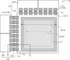
図13には、本変形例の搬送治具500によりセンサ基板12及び回路基板(信号処理基板300)を保持した状態の一例を示す。
図14には、本変形例の搬送治具500によりセンサ基板12及び回路基板(信号処理基板300)を保持した状態の一例を示す。
図15には、本変形例の搬送治具500によりセンサ基板12及び回路基板(信号処理基板300)を保持した状態の一例を示す。
図16には、本変形例の放射線検出器10の製造工程の流れの一例を示すフローチャートが示されている。図16に示すように、本変形例の製造工程は、上記形態の製造工程(図5参照)と異なり、S24の吸着搬送工程の後に変換層形成工程S26を実施する。
10 放射線検出器
11 基材、11A 第1の面、11B 第2の面
12 センサ基板
14 変換層、14A 中央部、14B 周縁部
30 画素
32 TFT(スイッチング素子)
34 センサ部
35 画素領域
36 信号配線
38 走査配線
39 共通配線
40 補強部材
42 粘着剤
60 粘着層
62 反射層
64 接着層
66 保護層
100 制御部、100A CPU、100B メモリ、100C 記憶部
102 駆動部
104 信号処理部
106 画像メモリ
108 電源部
110 制御基板
112、112A、112B フレキシブルケーブル
113 端子
116 中板
120 筐体、120A 照射面
200 駆動基板
210 駆動IC
300 信号処理基板
301 孔
310 信号処理IC
400 支持体
402 剥離層
500 搬送治具
510 吸着部
512 保持部
520、554 吸着部材
521、555 吸着パッド
522 軸部
524 アダプタ
526 緩衝部材
528 ナット
530 接続部材
532 ホース
540 ベース
550 保持部材
552 支持部
558 ピン
570 搬送ステージ
Claims (12)
- 支持体に可撓性の基材を設け、放射線から変換された光に応じて発生した電荷を蓄積する複数の画素が前記基材の第1の面の画素領域に設けられた基板を形成する工程と、
前記基材の前記第1の面に、ケーブルを電気的に接続するための端子部を設ける工程と、
前記画素から前記電荷を読み出すため、または前記画素を駆動させるための回路基板を、前記ケーブルを介して前記端子部に電気的に接続する工程と、
前記ケーブルを介して前記端子部が前記回路基板に電気的に接続された前記基板を、前記支持体から剥離する工程と、
複数の吸着部材を有する吸着部と、保持部材を有する保持部とを含む搬送治具を用い、前記複数の吸着部材により前記基材の前記第1の面、または前記第1の面と反対側の第2の面を吸着することにより支持し、かつ前記保持部材により前記回路基板を保持した状態で、前記支持体から剥離した前記基板を搬送する工程と、
を備えた放射線画像撮影装置の製造方法。 - 前記基材の前記第1の面に、前記放射線を光に変換する変換層を設ける工程をさらに備え、
前記搬送治具により前記基板を搬送する工程では、前記変換層が設けられた前記基板を前記搬送治具により搬送する、
請求項1に記載の放射線画像撮影装置の製造方法。 - 前記搬送治具により前記基板を搬送した後、前記基材の前記第1の面に、前記放射線を光に変換する変換層を設ける工程をさらに備えた、
請求項1に記載の放射線画像撮影装置の製造方法。 - 前記基材の前記第2の面に、前記基材の強度を補強する補強部材を設ける工程をさらに備えた、
請求項1から請求項3のいずれか1項に記載の放射線画像撮影装置の製造方法。 - 前記搬送治具の前記保持部材は、前記ケーブルを折り返した状態で前記回路基板を載置することにより前記回路基板を保持する
請求項1から請求項4のいずれか1項に記載の放射線画像撮影装置の製造方法。 - 前記搬送治具の前記保持部材は、前記ケーブルを伸ばした状態で前記回路基板を載置することにより前記回路基板を保持する
請求項1から請求項4のいずれか1項に記載の放射線画像撮影装置の製造方法。 - 前記回路基板には孔が設けられ、
また、前記搬送治具の前記保持部材にはピンが設けられており、
前記搬送治具は、前記回路基板の前記孔に前記ピンを挿通することにより前記回路基板を保持する
請求項1から請求項4のいずれか1項に記載の放射線画像撮影装置の製造方法。 - 前記搬送治具の前記保持部材は、吸着によって前記回路基板を保持する
請求項1から請求項4のいずれか1項に記載の放射線画像撮影装置の製造方法。 - 前記搬送治具は、前記基材の前記第2の面の全面を前記複数の吸着部材により支持する
請求項1から請求項8のいずれか1項に記載の放射線画像撮影装置の製造方法。 - 前記搬送治具の前記複数の吸着部材の各々には、前記基材の凹凸を吸収する緩衝部材が設けられている、
請求項1から請求項9のいずれか1項に記載の放射線画像撮影装置の製造方法。 - 可撓性の基材の第1の面の画素領域に、放射線から変換された光に応じて発生した電荷を蓄積する複数の画素が設けられ、かつ前記画素から前記電荷を読み出すため、または前記画素を駆動させるための回路基板がケーブルを介して電気的に接続された端子部が設けられた基板を搬送する搬送治具であって、
前記基材の前記第1の面、または前記第1の面と反対側の第2の面を吸着する複数の吸着部材を有する吸着部と、
前記回路基板を保持する保持部材を有する保持部と、
を含む搬送治具。 - 前記複数の吸着部材の各々には、前記基材の凹凸を吸収する緩衝部材が設けられている、
請求項11に記載の搬送治具。
Priority Applications (3)
| Application Number | Priority Date | Filing Date | Title |
|---|---|---|---|
| JP2020161416A JP7261777B2 (ja) | 2020-09-25 | 2020-09-25 | 放射線画像撮影装置の製造方法及び搬送治具 |
| US17/480,158 US20220102399A1 (en) | 2020-09-25 | 2021-09-21 | Method of manufacturing radiographic imaging apparatus, and transport jig |
| TW110135307A TW202212863A (zh) | 2020-09-25 | 2021-09-23 | 放射線圖像攝影裝置的製造方法及搬運治具 |
Applications Claiming Priority (1)
| Application Number | Priority Date | Filing Date | Title |
|---|---|---|---|
| JP2020161416A JP7261777B2 (ja) | 2020-09-25 | 2020-09-25 | 放射線画像撮影装置の製造方法及び搬送治具 |
Publications (3)
| Publication Number | Publication Date |
|---|---|
| JP2022054302A JP2022054302A (ja) | 2022-04-06 |
| JP2022054302A5 JP2022054302A5 (ja) | 2022-08-30 |
| JP7261777B2 true JP7261777B2 (ja) | 2023-04-20 |
Family
ID=80821480
Family Applications (1)
| Application Number | Title | Priority Date | Filing Date |
|---|---|---|---|
| JP2020161416A Active JP7261777B2 (ja) | 2020-09-25 | 2020-09-25 | 放射線画像撮影装置の製造方法及び搬送治具 |
Country Status (3)
| Country | Link |
|---|---|
| US (1) | US20220102399A1 (ja) |
| JP (1) | JP7261777B2 (ja) |
| TW (1) | TW202212863A (ja) |
Citations (2)
| Publication number | Priority date | Publication date | Assignee | Title |
|---|---|---|---|---|
| JP2006156849A (ja) | 2004-11-30 | 2006-06-15 | Shibaura Mechatronics Corp | 表示装置の組み立て装置及び表示装置の組み立て方法 |
| WO2020162637A1 (ja) | 2019-02-08 | 2020-08-13 | 富士フイルム株式会社 | 放射線検出器の製造方法及び放射線画像撮影装置 |
Family Cites Families (2)
| Publication number | Priority date | Publication date | Assignee | Title |
|---|---|---|---|---|
| JP2015068653A (ja) * | 2013-09-26 | 2015-04-13 | キヤノン株式会社 | 放射線撮像装置、その製造方法及び放射線検査装置 |
| CN108966641B (zh) * | 2017-03-22 | 2022-02-22 | 富士胶片株式会社 | 放射线检测器以及放射线图像摄影装置 |
-
2020
- 2020-09-25 JP JP2020161416A patent/JP7261777B2/ja active Active
-
2021
- 2021-09-21 US US17/480,158 patent/US20220102399A1/en active Pending
- 2021-09-23 TW TW110135307A patent/TW202212863A/zh unknown
Patent Citations (2)
| Publication number | Priority date | Publication date | Assignee | Title |
|---|---|---|---|---|
| JP2006156849A (ja) | 2004-11-30 | 2006-06-15 | Shibaura Mechatronics Corp | 表示装置の組み立て装置及び表示装置の組み立て方法 |
| WO2020162637A1 (ja) | 2019-02-08 | 2020-08-13 | 富士フイルム株式会社 | 放射線検出器の製造方法及び放射線画像撮影装置 |
Also Published As
| Publication number | Publication date |
|---|---|
| TW202212863A (zh) | 2022-04-01 |
| US20220102399A1 (en) | 2022-03-31 |
| JP2022054302A (ja) | 2022-04-06 |
Similar Documents
| Publication | Publication Date | Title |
|---|---|---|
| TWI805714B (zh) | 放射線檢測器、放射線圖像攝影裝置以及製造方法 | |
| TWI821460B (zh) | 放射線檢測器、放射線圖像攝影裝置及製造方法 | |
| JP2022101584A (ja) | 放射線検出器、放射線画像撮影装置及び放射線検出器の製造方法 | |
| US11802981B2 (en) | Method of manufacturing radiation detector and radiographic imaging apparatus | |
| JP7451787B2 (ja) | 放射線画像撮影装置 | |
| JP7261777B2 (ja) | 放射線画像撮影装置の製造方法及び搬送治具 | |
| JP7208941B2 (ja) | 放射線検出器、放射線画像撮影装置、及び放射線検出器の製造方法 | |
| JP7230202B2 (ja) | 放射線検出器及び放射線画像撮影装置 | |
| JP7282922B2 (ja) | 放射線画像撮影装置の製造方法 | |
| JP7332784B2 (ja) | 放射線検出器、及び放射線画像撮影装置 | |
| TWI834890B (zh) | 放射線檢測器及放射線圖像攝影裝置 | |
| WO2021033663A1 (ja) | 放射線検出器の製造方法 | |
| US11877875B2 (en) | Radiation detector, radiographic imaging apparatus, and method of manufacturing radiation detector | |
| JP7303368B2 (ja) | 放射線検出器、放射線画像撮影装置、及び放射線検出器の製造方法 | |
| JP2023001752A (ja) | 放射線画像撮影装置 |
Legal Events
| Date | Code | Title | Description |
|---|---|---|---|
| A521 | Request for written amendment filed |
Free format text: JAPANESE INTERMEDIATE CODE: A523 Effective date: 20220822 |
|
| A621 | Written request for application examination |
Free format text: JAPANESE INTERMEDIATE CODE: A621 Effective date: 20220822 |
|
| A977 | Report on retrieval |
Free format text: JAPANESE INTERMEDIATE CODE: A971007 Effective date: 20230307 |
|
| TRDD | Decision of grant or rejection written | ||
| A01 | Written decision to grant a patent or to grant a registration (utility model) |
Free format text: JAPANESE INTERMEDIATE CODE: A01 Effective date: 20230314 |
|
| A61 | First payment of annual fees (during grant procedure) |
Free format text: JAPANESE INTERMEDIATE CODE: A61 Effective date: 20230410 |
|
| R150 | Certificate of patent or registration of utility model |
Ref document number: 7261777 Country of ref document: JP Free format text: JAPANESE INTERMEDIATE CODE: R150 |