JP7261777B2 - Manufacturing method and transport jig for radiographic imaging device - Google Patents
Manufacturing method and transport jig for radiographic imaging device Download PDFInfo
- Publication number
- JP7261777B2 JP7261777B2 JP2020161416A JP2020161416A JP7261777B2 JP 7261777 B2 JP7261777 B2 JP 7261777B2 JP 2020161416 A JP2020161416 A JP 2020161416A JP 2020161416 A JP2020161416 A JP 2020161416A JP 7261777 B2 JP7261777 B2 JP 7261777B2
- Authority
- JP
- Japan
- Prior art keywords
- substrate
- circuit board
- base material
- radiographic imaging
- manufacturing
- Prior art date
- Legal status (The legal status is an assumption and is not a legal conclusion. Google has not performed a legal analysis and makes no representation as to the accuracy of the status listed.)
- Active
Links
- 238000003384 imaging method Methods 0.000 title claims description 63
- 238000004519 manufacturing process Methods 0.000 title claims description 56
- 239000000758 substrate Substances 0.000 claims description 157
- 239000000463 material Substances 0.000 claims description 119
- 238000006243 chemical reaction Methods 0.000 claims description 80
- 230000005855 radiation Effects 0.000 claims description 75
- 238000000034 method Methods 0.000 claims description 61
- 238000001179 sorption measurement Methods 0.000 claims description 56
- 230000003014 reinforcing effect Effects 0.000 claims description 43
- 230000008569 process Effects 0.000 claims description 29
- 230000004044 response Effects 0.000 claims description 4
- 239000010410 layer Substances 0.000 description 107
- 238000012545 processing Methods 0.000 description 44
- 238000012546 transfer Methods 0.000 description 25
- 239000012790 adhesive layer Substances 0.000 description 23
- 229920005989 resin Polymers 0.000 description 19
- 239000011347 resin Substances 0.000 description 19
- 239000010408 film Substances 0.000 description 16
- 238000005452 bending Methods 0.000 description 15
- XQPRBTXUXXVTKB-UHFFFAOYSA-M caesium iodide Chemical compound [I-].[Cs+] XQPRBTXUXXVTKB-UHFFFAOYSA-M 0.000 description 15
- 230000004048 modification Effects 0.000 description 15
- 238000012986 modification Methods 0.000 description 15
- 239000005020 polyethylene terephthalate Substances 0.000 description 14
- 229920000139 polyethylene terephthalate Polymers 0.000 description 14
- 230000006870 function Effects 0.000 description 12
- 239000000853 adhesive Substances 0.000 description 10
- 230000001070 adhesive effect Effects 0.000 description 10
- 239000011241 protective layer Substances 0.000 description 9
- 230000015572 biosynthetic process Effects 0.000 description 7
- 229910052782 aluminium Inorganic materials 0.000 description 6
- XAGFODPZIPBFFR-UHFFFAOYSA-N aluminium Chemical compound [Al] XAGFODPZIPBFFR-UHFFFAOYSA-N 0.000 description 6
- 238000010586 diagram Methods 0.000 description 5
- 229910052751 metal Inorganic materials 0.000 description 5
- 239000002184 metal Substances 0.000 description 5
- 230000002093 peripheral effect Effects 0.000 description 5
- 239000004417 polycarbonate Substances 0.000 description 5
- -1 polyethylene terephthalate Polymers 0.000 description 5
- OKTJSMMVPCPJKN-UHFFFAOYSA-N Carbon Chemical compound [C] OKTJSMMVPCPJKN-UHFFFAOYSA-N 0.000 description 4
- 229910052799 carbon Inorganic materials 0.000 description 4
- 239000010419 fine particle Substances 0.000 description 4
- 229920003023 plastic Polymers 0.000 description 4
- 239000004033 plastic Substances 0.000 description 4
- 229910010413 TiO 2 Inorganic materials 0.000 description 3
- NIXOWILDQLNWCW-UHFFFAOYSA-N acrylic acid group Chemical group C(C=C)(=O)O NIXOWILDQLNWCW-UHFFFAOYSA-N 0.000 description 3
- 229910021417 amorphous silicon Inorganic materials 0.000 description 3
- 239000013078 crystal Substances 0.000 description 3
- 239000011521 glass Substances 0.000 description 3
- 238000003860 storage Methods 0.000 description 3
- 238000012360 testing method Methods 0.000 description 3
- 238000001947 vapour-phase growth Methods 0.000 description 3
- XKRFYHLGVUSROY-UHFFFAOYSA-N Argon Chemical compound [Ar] XKRFYHLGVUSROY-UHFFFAOYSA-N 0.000 description 2
- RYGMFSIKBFXOCR-UHFFFAOYSA-N Copper Chemical compound [Cu] RYGMFSIKBFXOCR-UHFFFAOYSA-N 0.000 description 2
- 239000004831 Hot glue Substances 0.000 description 2
- 239000004734 Polyphenylene sulfide Substances 0.000 description 2
- 239000004743 Polypropylene Substances 0.000 description 2
- PPBRXRYQALVLMV-UHFFFAOYSA-N Styrene Chemical compound C=CC1=CC=CC=C1 PPBRXRYQALVLMV-UHFFFAOYSA-N 0.000 description 2
- 238000010521 absorption reaction Methods 0.000 description 2
- TZCXTZWJZNENPQ-UHFFFAOYSA-L barium sulfate Chemical compound [Ba+2].[O-]S([O-])(=O)=O TZCXTZWJZNENPQ-UHFFFAOYSA-L 0.000 description 2
- 239000003990 capacitor Substances 0.000 description 2
- 230000008859 change Effects 0.000 description 2
- 238000005229 chemical vapour deposition Methods 0.000 description 2
- 229910052802 copper Inorganic materials 0.000 description 2
- 239000010949 copper Substances 0.000 description 2
- 230000007423 decrease Effects 0.000 description 2
- 229920006351 engineering plastic Polymers 0.000 description 2
- 239000005038 ethylene vinyl acetate Substances 0.000 description 2
- 229920006244 ethylene-ethyl acrylate Polymers 0.000 description 2
- 238000009434 installation Methods 0.000 description 2
- 238000011900 installation process Methods 0.000 description 2
- 238000005259 measurement Methods 0.000 description 2
- 239000011368 organic material Substances 0.000 description 2
- 239000005026 oriented polypropylene Substances 0.000 description 2
- 239000012994 photoredox catalyst Substances 0.000 description 2
- 229920003207 poly(ethylene-2,6-naphthalate) Polymers 0.000 description 2
- 229920001200 poly(ethylene-vinyl acetate) Polymers 0.000 description 2
- 239000011112 polyethylene naphthalate Substances 0.000 description 2
- 229920001955 polyphenylene ether Polymers 0.000 description 2
- 229920000069 polyphenylene sulfide Polymers 0.000 description 2
- 229920001155 polypropylene Polymers 0.000 description 2
- 239000004800 polyvinyl chloride Substances 0.000 description 2
- 229920000915 polyvinyl chloride Polymers 0.000 description 2
- 238000005070 sampling Methods 0.000 description 2
- 239000011734 sodium Substances 0.000 description 2
- NIXOWILDQLNWCW-UHFFFAOYSA-M Acrylate Chemical compound [O-]C(=O)C=C NIXOWILDQLNWCW-UHFFFAOYSA-M 0.000 description 1
- 239000004925 Acrylic resin Substances 0.000 description 1
- 229920000178 Acrylic resin Polymers 0.000 description 1
- 229910018072 Al 2 O 3 Inorganic materials 0.000 description 1
- DGAQECJNVWCQMB-PUAWFVPOSA-M Ilexoside XXIX Chemical compound C[C@@H]1CC[C@@]2(CC[C@@]3(C(=CC[C@H]4[C@]3(CC[C@@H]5[C@@]4(CC[C@@H](C5(C)C)OS(=O)(=O)[O-])C)C)[C@@H]2[C@]1(C)O)C)C(=O)O[C@H]6[C@@H]([C@H]([C@@H]([C@H](O6)CO)O)O)O.[Na+] DGAQECJNVWCQMB-PUAWFVPOSA-M 0.000 description 1
- 239000004677 Nylon Substances 0.000 description 1
- 239000004642 Polyimide Substances 0.000 description 1
- 229910004298 SiO 2 Inorganic materials 0.000 description 1
- 239000004809 Teflon Substances 0.000 description 1
- 229920006362 Teflon® Polymers 0.000 description 1
- 239000002253 acid Substances 0.000 description 1
- 239000003522 acrylic cement Substances 0.000 description 1
- 229920000122 acrylonitrile butadiene styrene Polymers 0.000 description 1
- 229910052786 argon Inorganic materials 0.000 description 1
- 239000011230 binding agent Substances 0.000 description 1
- 239000000872 buffer Substances 0.000 description 1
- MTAZNLWOLGHBHU-UHFFFAOYSA-N butadiene-styrene rubber Chemical compound C=CC=C.C=CC1=CC=CC=C1 MTAZNLWOLGHBHU-UHFFFAOYSA-N 0.000 description 1
- 239000004918 carbon fiber reinforced polymer Substances 0.000 description 1
- 238000000576 coating method Methods 0.000 description 1
- 230000008602 contraction Effects 0.000 description 1
- 229920001577 copolymer Polymers 0.000 description 1
- 238000013016 damping Methods 0.000 description 1
- 238000003745 diagnosis Methods 0.000 description 1
- 230000000694 effects Effects 0.000 description 1
- 238000000295 emission spectrum Methods 0.000 description 1
- UHESRSKEBRADOO-UHFFFAOYSA-N ethyl carbamate;prop-2-enoic acid Chemical compound OC(=O)C=C.CCOC(N)=O UHESRSKEBRADOO-UHFFFAOYSA-N 0.000 description 1
- 229920006242 ethylene acrylic acid copolymer Polymers 0.000 description 1
- 239000005042 ethylene-ethyl acrylate Substances 0.000 description 1
- 239000011888 foil Substances 0.000 description 1
- 230000005484 gravity Effects 0.000 description 1
- 238000009499 grossing Methods 0.000 description 1
- 238000010438 heat treatment Methods 0.000 description 1
- 229910010272 inorganic material Inorganic materials 0.000 description 1
- 239000011147 inorganic material Substances 0.000 description 1
- 238000003475 lamination Methods 0.000 description 1
- 239000011159 matrix material Substances 0.000 description 1
- 239000012528 membrane Substances 0.000 description 1
- 229910044991 metal oxide Inorganic materials 0.000 description 1
- 150000004706 metal oxides Chemical class 0.000 description 1
- 125000002496 methyl group Chemical group [H]C([H])([H])* 0.000 description 1
- 229920001778 nylon Polymers 0.000 description 1
- 230000003287 optical effect Effects 0.000 description 1
- 239000002245 particle Substances 0.000 description 1
- 230000000149 penetrating effect Effects 0.000 description 1
- 230000035515 penetration Effects 0.000 description 1
- 229920000052 poly(p-xylylene) Polymers 0.000 description 1
- 229920000515 polycarbonate Polymers 0.000 description 1
- 229920001721 polyimide Polymers 0.000 description 1
- KCTAWXVAICEBSD-UHFFFAOYSA-N prop-2-enoyloxy prop-2-eneperoxoate Chemical compound C=CC(=O)OOOC(=O)C=C KCTAWXVAICEBSD-UHFFFAOYSA-N 0.000 description 1
- 238000000926 separation method Methods 0.000 description 1
- 229910052814 silicon oxide Inorganic materials 0.000 description 1
- 239000013464 silicone adhesive Substances 0.000 description 1
- 229910052708 sodium Inorganic materials 0.000 description 1
- 238000004544 sputter deposition Methods 0.000 description 1
- 229910052716 thallium Inorganic materials 0.000 description 1
- BKVIYDNLLOSFOA-UHFFFAOYSA-N thallium Chemical compound [Tl] BKVIYDNLLOSFOA-UHFFFAOYSA-N 0.000 description 1
- 229920001169 thermoplastic Polymers 0.000 description 1
- 229920005992 thermoplastic resin Polymers 0.000 description 1
- 239000004416 thermosoftening plastic Substances 0.000 description 1
- 239000010409 thin film Substances 0.000 description 1
- 230000007704 transition Effects 0.000 description 1
- 238000001771 vacuum deposition Methods 0.000 description 1
- 239000012463 white pigment Substances 0.000 description 1
Images


Classifications
-
- H—ELECTRICITY
- H01—ELECTRIC ELEMENTS
- H01L—SEMICONDUCTOR DEVICES NOT COVERED BY CLASS H10
- H01L27/00—Devices consisting of a plurality of semiconductor or other solid-state components formed in or on a common substrate
- H01L27/14—Devices consisting of a plurality of semiconductor or other solid-state components formed in or on a common substrate including semiconductor components sensitive to infrared radiation, light, electromagnetic radiation of shorter wavelength or corpuscular radiation and specially adapted either for the conversion of the energy of such radiation into electrical energy or for the control of electrical energy by such radiation
- H01L27/144—Devices controlled by radiation
- H01L27/146—Imager structures
- H01L27/14601—Structural or functional details thereof
- H01L27/14625—Optical elements or arrangements associated with the device
-
- H—ELECTRICITY
- H01—ELECTRIC ELEMENTS
- H01L—SEMICONDUCTOR DEVICES NOT COVERED BY CLASS H10
- H01L27/00—Devices consisting of a plurality of semiconductor or other solid-state components formed in or on a common substrate
- H01L27/14—Devices consisting of a plurality of semiconductor or other solid-state components formed in or on a common substrate including semiconductor components sensitive to infrared radiation, light, electromagnetic radiation of shorter wavelength or corpuscular radiation and specially adapted either for the conversion of the energy of such radiation into electrical energy or for the control of electrical energy by such radiation
- H01L27/144—Devices controlled by radiation
- H01L27/146—Imager structures
- H01L27/14643—Photodiode arrays; MOS imagers
- H01L27/14658—X-ray, gamma-ray or corpuscular radiation imagers
- H01L27/14663—Indirect radiation imagers, e.g. using luminescent members
-
- H—ELECTRICITY
- H01—ELECTRIC ELEMENTS
- H01L—SEMICONDUCTOR DEVICES NOT COVERED BY CLASS H10
- H01L27/00—Devices consisting of a plurality of semiconductor or other solid-state components formed in or on a common substrate
- H01L27/14—Devices consisting of a plurality of semiconductor or other solid-state components formed in or on a common substrate including semiconductor components sensitive to infrared radiation, light, electromagnetic radiation of shorter wavelength or corpuscular radiation and specially adapted either for the conversion of the energy of such radiation into electrical energy or for the control of electrical energy by such radiation
- H01L27/144—Devices controlled by radiation
- H01L27/146—Imager structures
- H01L27/14683—Processes or apparatus peculiar to the manufacture or treatment of these devices or parts thereof
- H01L27/1469—Assemblies, i.e. hybrid integration
-
- H—ELECTRICITY
- H01—ELECTRIC ELEMENTS
- H01L—SEMICONDUCTOR DEVICES NOT COVERED BY CLASS H10
- H01L31/00—Semiconductor devices sensitive to infrared radiation, light, electromagnetic radiation of shorter wavelength or corpuscular radiation and specially adapted either for the conversion of the energy of such radiation into electrical energy or for the control of electrical energy by such radiation; Processes or apparatus specially adapted for the manufacture or treatment thereof or of parts thereof; Details thereof
- H01L31/18—Processes or apparatus specially adapted for the manufacture or treatment of these devices or of parts thereof
- H01L31/1892—Processes or apparatus specially adapted for the manufacture or treatment of these devices or of parts thereof methods involving the use of temporary, removable substrates
- H01L31/1896—Processes or apparatus specially adapted for the manufacture or treatment of these devices or of parts thereof methods involving the use of temporary, removable substrates for thin-film semiconductors
Landscapes
- Engineering & Computer Science (AREA)
- Power Engineering (AREA)
- Physics & Mathematics (AREA)
- Computer Hardware Design (AREA)
- General Physics & Mathematics (AREA)
- Condensed Matter Physics & Semiconductors (AREA)
- Electromagnetism (AREA)
- Microelectronics & Electronic Packaging (AREA)
- Health & Medical Sciences (AREA)
- Toxicology (AREA)
- Manufacturing & Machinery (AREA)
- Measurement Of Radiation (AREA)
- Apparatus For Radiation Diagnosis (AREA)
Description
本開示は、放射線画像撮影装置の製造方法及び搬送治具に関する。 The present disclosure relates to a method of manufacturing a radiographic imaging apparatus and a transport jig.
従来、医療診断を目的とした放射線撮影を行う放射線画像撮影装置が知られている。このような放射線画像撮影装置には、被写体を透過した放射線を検出し放射線画像を生成するための放射線検出器が用いられている。 2. Description of the Related Art Conventionally, radiographic imaging apparatuses that perform radiographic imaging for the purpose of medical diagnosis are known. Radiation detectors for detecting radiation transmitted through a subject and generating a radiation image are used in such radiographic imaging apparatuses.
放射線検出器としては、放射線を光に変換するシンチレータ等の変換層と、変換層で変換された光に応じて発生した電荷を蓄積する複数の画素が設けられた基板と、を備えたものがある。このような放射線検出器のセンサ基板の基材として、可撓性の基材を用いたものが知られている。可撓性の基材を用いることにより、放射線画像撮影装置を軽量化でき、また、被写体の撮影が容易となる場合がある。 The radiation detector includes a conversion layer such as a scintillator that converts radiation into light, and a substrate provided with a plurality of pixels that accumulate charges generated according to the light converted by the conversion layer. be. As a base material for the sensor substrate of such a radiation detector, one using a flexible base material is known. By using a flexible base material, the weight of the radiographic imaging apparatus can be reduced, and imaging of a subject may be facilitated.
特許文献1には、可撓性の基材を用いたセンサ基板を備えた放射線検出器の製造方法が記載されている。特許文献1に記載の製造方法は、支持体上に可撓性の基材を設けて基板及を形成した後、支持体から基板を剥離する工程を備える。
特許文献1に記載の技術では、支持体から剥離した基板を搬送する工程が必要となるが、基材が可撓性を有するため、搬送中に基材が撓む等するため、基板を安定した状態で搬送し難い場合がある。また、回路基板が電気的に接続された状態の基板を搬送する場合、可撓性の基材を用いた基板と回路基板とは、別体であるため、安定した状態で両者の搬送し難い場合があった。
The technique described in
本開示は、可撓性の基材を用いた基板と、回路基板とを各々安定した状態で搬送することができる放射線画像撮影装置の製造方法及び搬送治具を提供することを目的とする。 An object of the present disclosure is to provide a method for manufacturing a radiographic image capturing apparatus and a transport jig capable of transporting a board using a flexible base material and a circuit board in a stable state.
上記目的を達成するために、本開示の第1の態様の放射線画像撮影装置の製造方法は、支持体に可撓性の基材を設け、放射線から変換された光に応じて発生した電荷を蓄積する複数の画素が基材の第1の面の画素領域に設けられた基板を形成する工程と、基材の第1の面に、ケーブルを電気的に接続するための端子部を設ける工程と、画素から電荷を読み出すため、または画素を駆動させるための回路基板を、ケーブルを介して端子部に電気的に接続する工程と、ケーブルを介して端子部が回路基板に電気的に接続された基板を、支持体から剥離する工程と、複数の吸着部材を有する吸着部と、保持部材を有する保持部とを含む搬送治具を用い、複数の吸着部材により基材の第1の面、または第1の面と反対側の第2の面を吸着することにより支持し、かつ保持部材により回路基板を保持した状態で、支持体から剥離した基板を搬送する工程と、を備える。 In order to achieve the above object, a method for manufacturing a radiographic imaging device according to a first aspect of the present disclosure provides a support with a flexible base material, and charges generated in accordance with light converted from radiation. A step of forming a substrate in which a plurality of pixels to be accumulated are provided in a pixel region on a first surface of a base material; and a step of providing a terminal portion for electrically connecting a cable to the first surface of the base material. a step of electrically connecting a circuit board for reading charges from the pixels or driving the pixels to the terminal portion via a cable; and electrically connecting the terminal portion to the circuit board via the cable. The first surface of the substrate is separated from the support by the plurality of adsorption members using a transfer jig including a step of separating the substrate from the support, an adsorption portion having a plurality of adsorption members, and a holding portion having a holding member. Alternatively, the step of conveying the substrate peeled from the support while supporting the second surface opposite to the first surface by suction and holding the circuit board by the holding member.
また、本開示の第2の態様の放射線画像撮影装置の製造方法は、第1の態様の放射線画像撮影装置の製造方法において、基材の第1の面に、放射線を光に変換する変換層を設ける工程をさらに備え、搬送治具により基板を搬送する工程では、変換層が設けられた基板を搬送治具により搬送する。 A method for manufacturing a radiographic imaging device according to a second aspect of the present disclosure is the method for manufacturing a radiographic imaging device according to the first aspect, wherein a conversion layer for converting radiation into light is provided on the first surface of the substrate. and in the step of transporting the substrate by the transport jig, the substrate provided with the conversion layer is transported by the transport jig.
また、本開示の第3の態様の放射線画像撮影装置の製造方法は、第1の態様の放射線画像撮影装置の製造方法において、搬送治具により基板を搬送した後、基材の第1の面に、放射線を光に変換する変換層を設ける工程をさらに備える。 A method for manufacturing a radiographic imaging device according to a third aspect of the present disclosure is the method for manufacturing a radiographic imaging device according to the first aspect, wherein after the substrate is transferred by the transfer jig, the first surface of the base material is , further comprising the step of providing a conversion layer for converting radiation into light.
また、本開示の第4の態様の放射線画像撮影装置の製造方法は、第1の態様から第3の態様のいずれか1態様の放射線画像撮影装置の製造方法において、基材の第2の面に、基材の強度を補強する補強部材を設ける工程をさらに備える。 Further, a method for manufacturing a radiographic imaging device according to a fourth aspect of the present disclosure is a method for manufacturing a radiographic imaging device according to any one of the first to third aspects, wherein the second surface of the base material is and further comprising the step of providing a reinforcing member for reinforcing the strength of the base material.
また、本開示の第5の態様の放射線画像撮影装置の製造方法は、第1の態様から第4の態様のいずれか1態様の放射線画像撮影装置の製造方法において、搬送治具の保持部材は、ケーブルを折り返した状態で回路基板を載置することにより回路基板を保持する。 A method for manufacturing a radiographic imaging device according to a fifth aspect of the present disclosure is the method for manufacturing a radiographic imaging device according to any one of the first to fourth aspects, wherein the holding member of the conveying jig is The circuit board is held by placing the circuit board with the cable folded back.
また、本開示の第6の態様の放射線画像撮影装置の製造方法は、第1の態様から第4の態様のいずれか1態様の放射線画像撮影装置の製造方法において、搬送治具の保持部材は、ケーブルを伸ばした状態で回路基板を載置することにより回路基板を保持する。 A method for manufacturing a radiographic imaging device according to a sixth aspect of the present disclosure is a method for manufacturing a radiographic imaging device according to any one of the first aspect to the fourth aspect, wherein the holding member of the conveying jig is , the circuit board is held by placing the circuit board with the cable extended.
また、本開示の第7の態様の放射線画像撮影装置の製造方法は、第1の態様から第4の態様のいずれか1態様の放射線画像撮影装置の製造方法において、回路基板には孔が設けられ、また、搬送治具の保持部材にはピンが設けられており、搬送治具は、回路基板の孔にピンを挿通することにより回路基板を保持する。 A method for manufacturing a radiographic imaging device according to a seventh aspect of the present disclosure is the method for manufacturing a radiographic imaging device according to any one of the first to fourth aspects, wherein the circuit board is provided with a hole. A holding member of the carrier jig is provided with a pin, and the carrier jig holds the circuit board by inserting the pin into the hole of the circuit board.
また、本開示の第8の態様の放射線画像撮影装置の製造方法は、第1の態様から第4の態様のいずれか1態様の放射線画像撮影装置の製造方法において、搬送治具の保持部材は、吸着によって回路基板を保持する。 A method for manufacturing a radiographic imaging device according to an eighth aspect of the present disclosure is a method for manufacturing a radiographic imaging device according to any one of the first to fourth aspects, wherein the holding member of the conveying jig is , hold the circuit board by suction.
また、本開示の第9の態様の放射線画像撮影装置の製造方法は、第1の態様から第8の態様のいずれか1態様の放射線画像撮影装置の製造方法において、搬送治具は、基材の第2の面の全面を複数の吸着部材により支持する。 Further, a method for manufacturing a radiographic imaging device according to a ninth aspect of the present disclosure is a method for manufacturing a radiographic imaging device according to any one aspect of the first to eighth aspects, wherein the conveying jig comprises a base material The entire second surface of is supported by a plurality of adsorption members.
また、本開示の第10の態様の放射線画像撮影装置の製造方法は、第1の態様から第9の態様のいずれか1態様の放射線画像撮影装置の製造方法において、搬送治具の複数の吸着部材の各々には、基材の凹凸を吸収する緩衝部材が設けられている。 Further, a method for manufacturing a radiographic imaging device according to a tenth aspect of the present disclosure is the method for manufacturing a radiographic imaging device according to any one of the first to ninth aspects, wherein the suction of the conveying jig is Each member is provided with a cushioning member that absorbs the unevenness of the base material.
また、本開示の第11の態様の搬送治具は、可撓性の基材の第1の面の画素領域に、放射線から変換された光に応じて発生した電荷を蓄積する複数の画素が設けられ、かつ画素から電荷を読み出すため、または画素を駆動させるための回路基板がケーブルを介して電気的に接続された端子部が設けられた基板を搬送する搬送治具であって、基材の第1の面、または第1の面と反対側の第2の面を吸着する複数の吸着部材を有する吸着部と、 Further, in the transport jig according to the eleventh aspect of the present disclosure, the pixel region on the first surface of the flexible base material has a plurality of pixels for accumulating charges generated in response to light converted from radiation. A carrier jig for carrying a substrate provided with a terminal section electrically connected via a cable to a circuit board for reading charges from pixels or driving the pixels, the substrate comprising: an adsorption unit having a plurality of adsorption members that adsorb a first surface of or a second surface opposite to the first surface;
回路基板を保持する保持部材を有する保持部と、を含む。 a holding portion having a holding member for holding the circuit board.
また、本開示の第12の態様の搬送治具は、第11の態様の搬送治具において、複数の吸着部材の各々には、基材の凹凸を吸収する緩衝部材が設けられている。 Further, a conveying jig according to a twelfth aspect of the present disclosure is the conveying jig according to the eleventh aspect, wherein each of the plurality of adsorption members is provided with a cushioning member that absorbs unevenness of the base material.
本開示によれば、可撓性の基材を用いた基板と、回路基板とを各々安定した状態で搬送することができる。 According to the present disclosure, a board using a flexible base material and a circuit board can be transported in a stable state.
以下、図面を参照して本発明の実施形態を詳細に説明する。なお、本実施形態は本発明を限定するものではない。 Hereinafter, embodiments of the present invention will be described in detail with reference to the drawings. In addition, this embodiment does not limit the present invention.
まず、本実施形態の放射線検出器及び放射線画像撮影装置について説明する。本実施形態の放射線検出器は、被写体を透過した放射線を検出して被写体の放射線画像を表す画像情報を出力する機能を有する。本実施形態の放射線検出器は、センサ基板と、放射線を光に変換する変換層と、を備えている(図3、放射線検出器10のセンサ基板12及び変換層14参照)。本実施形態のセンサ基板12が、本開示の基板の一例である。
First, a radiation detector and a radiographic image capturing apparatus according to this embodiment will be described. The radiation detector of this embodiment has a function of detecting radiation transmitted through a subject and outputting image information representing a radiation image of the subject. The radiation detector of this embodiment includes a sensor substrate and a conversion layer that converts radiation into light (see FIG. 3,
図1を参照して本実施形態の放射線画像撮影装置における電気系の構成の一例の概略を説明する。図1は、本実施形態の放射線画像撮影装置における電気系の要部構成の一例を示すブロック図である。 With reference to FIG. 1, an outline of an example of the configuration of the electrical system in the radiographic imaging apparatus of this embodiment will be described. FIG. 1 is a block diagram showing an example of the main configuration of an electrical system in a radiographic imaging apparatus according to this embodiment.
図1に示すように、本実施形態の放射線画像撮影装置1は、放射線検出器10、制御部100、駆動部102、信号処理部104、画像メモリ106、及び電源部108を備える。本実施形態の制御部100、駆動部102、及び信号処理部104の少なくとも1つが、本開示の回路部基板の一例である。以下、制御部100、駆動部102、及び信号処理部104を総称する場合、「回路基板」という。
As shown in FIG. 1, the
放射線検出器10は、センサ基板12と、放射線を光に変換する変換層14(図3参照)と、を備える。センサ基板12は、可撓性の基材11と、基材11の第1の面11Aに設けられた複数の画素30と、を備えている。なお、以下では、複数の画素30について、単に「画素30」という場合がある。
The
図1に示すように本実施形態の各画素30は、変換層が変換した光に応じて電荷を発生して蓄積するセンサ部34、及びセンサ部34にて蓄積された電荷を読み出すスイッチング素子32を備える。本実施形態では、一例として、薄膜トランジスタ(TFT:Thin Film Transistor)をスイッチング素子32として用いている。そのため、以下では、スイッチング素子32を「TFT32」という。本実施形態では、センサ部34及びTFT32が形成され、さらに平坦化された層として基材11の第1の面11Aに画素30が形成された層が設けられる。
As shown in FIG. 1, each
画素30は、センサ基板12の画素領域35に、一方向(図1の横方向に対応する走査配線方向、以下「行方向」ともいう)及び行方向に対する交差方向(図1の縦方向に対応する信号配線方向、以下「列方向」ともいう)に沿って二次元状に配置されている。図1では、画素30の配列を簡略化して示しているが、例えば、画素30は行方向及び列方向に1024個×1024個配置される。
The
また、放射線検出器10には、画素30の行毎に備えられた、TFT32のスイッチング状態(オン及びオフ)を制御するための複数の走査配線38と、画素30の列毎に備えられた、センサ部34に蓄積された電荷が読み出される複数の信号配線36と、が互いに交差して設けられている。複数の走査配線38の各々は、それぞれフレキシブルケーブル112Aを介して、駆動部102に接続されることにより、駆動部102から出力される、TFT32を駆動してスイッチング状態を制御する駆動信号が、複数の走査配線38の各々に流れる。また、複数の信号配線36の各々が、それぞれフレキシブルケーブル112Bを介して、信号処理部104に接続されることにより、各画素30から読み出された電荷が、電気信号として信号処理部104に出力される。信号処理部104は、入力された電気信号に応じた画像データを生成して出力する。なお、本実施形態においてフレキシブルケーブル112に関して「接続」という場合、電気的な接続を意味する。
In addition, the
信号処理部104には後述する制御部100が接続されており、信号処理部104から出力された画像データは制御部100に順次出力される。制御部100には画像メモリ106が接続されており、信号処理部104から順次出力された画像データは、制御部100による制御によって画像メモリ106に順次記憶される。画像メモリ106は所定の枚数分の画像データを記憶可能な記憶容量を有しており、放射線画像の撮影が行われる毎に、撮影によって得られた画像データが画像メモリ106に順次記憶される。
The
制御部100は、CPU(Central Processing Unit)100A、ROM(Read Only Memory)とRAM(Random Access Memory)等を含むメモリ100B、及びフラッシュメモリ等の不揮発性の記憶部100Cを備えている。制御部100の一例としては、マイクロコンピュータ等が挙げられる。制御部100は、放射線画像撮影装置1の全体の動作を制御する。
The
なお、本実施形態の放射線画像撮影装置1では、画像メモリ106及び制御部100等は、制御基板110に形成されている。
In addition, in the radiation
また、各画素30のセンサ部34には、各画素30にバイアス電圧を印加するために、共通配線39が信号配線36の配線方向に設けられている。共通配線39が、センサ基板12の外部のバイアス電源(図示省略)に接続されることにより、バイアス電源から各画素30にバイアス電圧が印加される。
Further, in the
電源部108は、制御部100、駆動部102、信号処理部104、画像メモリ106、及び電源部108等の各種素子や各種回路に電力を供給する。なお、図1では、錯綜を回避するために、電源部108と各種素子や各種回路を接続する配線の図示を省略している。
The
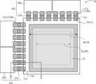
さらに、放射線検出器10について詳細に説明する。図2は、本実施形態の放射線検出器10を、基材11の第1の面11A側からみた平面図の一例である。また、図3は、図2における放射線検出器10のA-A線断面図の一例である。
Furthermore, the
基材11は、可撓性を有し、例えば、PI(PolyImide:ポリイミド)等のプラスチックを含む樹脂シートである。基材11の厚みは、材質の硬度、及びセンサ基板12の大きさ、すなわち第1の面11Aまたは第2の面11Bの面積等に応じて、所望の可撓性が得られる厚みであればよい。可撓性を有する例としては、矩形状の基材11単体の場合に、基材11の1辺を固定した状態で、固定した辺より10cm離れた位置で基材11の自重による重力で2mm以上、基材11が垂れ下がる(固定した辺の高さよりも低くなる)ものを指す。基材11が樹脂シートの場合の具体例としては、厚みが5μm~125μmのものであればよく、厚みが20μm~50μmのものであればより好ましい。
The
なお、基材11は、画素30の製造に耐え得る特性を有しており、本実施形態では、アモルファスシリコンTFT(a-Si TFT)の製造に耐え得る特性を有している。このような、基材11が有する特性としては、300℃~400℃における熱膨張率(CTE:Coefficient of Thermal Expansion)が、アモルファスシリコン(a-Si)ウェハと同程度(例えば、±5ppm/K)であることが好ましく、具体的には、20ppm/K以下であることが好ましい。また、基材11の熱収縮率としては、厚みが25μmの状態において400℃における熱収縮率が0.5%以下であることが好ましい。また、基材11の弾性率は、300℃~400℃間の温度領域において、一般的なPIが有する転移点を有さず、500℃における弾性率が1GPa以上であることが好ましい。
The
また、本実施形態の基材11は、自身による後方散乱線を抑制するために、平均粒子径が0.05μm以上、2.5μm以下の、後方散乱線を吸収する無機の微粒子を含む微粒子層を有することが好ましい。なおこのような無機の微粒子としては、樹脂製の基材11の場合、原子番号が、基材11である有機物を構成する原子よりも大きく、かつ30以下である無機物を用いることが好ましい。このような微粒子の具体例としては、原子番号が14のSiの酸化物であるSiO2、原子番号が12のMgの酸化物であるMgO、原子番号が13のAlの酸化物であるAl2O3、及び原子番号が22のTiの酸化物であるTiO2等が挙げられる。このような特性を有する樹脂シートの具体例としては、XENOMAX(登録商標)が挙げられる。
In addition, in order to suppress backscattered radiation by itself, the
なお、本実施形態における上記の厚みについては、マイクロメーターを用いて測定した。熱膨張率については、JIS K7197:1991に則して測定した。なお測定は、基材11の主面から、15度ずつ角度を変えて試験片を切り出し、切り出した各試験片について熱膨張率を測定し、最も高い値を基材11の熱膨張率とした。熱膨張率の測定は、MD(Machine Direction)方向およびTD(Transverse Direction)方向のそれぞれについて、-50℃~450℃において10℃間隔で行い、(ppm/℃)を(ppm/K)に換算した。熱膨張率の測定には、MACサイエンス社製 TMA4000S装置を用い、サンプル長さを10mm、サンプル幅を2mm、初荷重を34.5g/mm2、昇温速度を5℃/min、及び雰囲気をアルゴンとした。
Note that the above thickness in the present embodiment was measured using a micrometer. The coefficient of thermal expansion was measured according to JIS K7197:1991. For the measurement, test pieces were cut out from the main surface of the
所望の可撓性を有する基材11としては、樹脂シート等、樹脂製のものに限定されない。例えば、基材11は、厚みが比較的薄いガラス基板等であってもよい。基材11がガラス基板の場合の具体例としては、一般に、一辺が43cm程度のサイズでは、厚さが0.3mm以下ならば可撓性を有しているため、厚さが0.3mm以下のものであれば所望のガラス基板であってもよい。
The
図2及び図3に示すように、複数の画素30は、基材11の第1の面11Aに設けられている。本実施形態では、基材11の第1の面11Aにおける画素30が設けられた領域を画素領域35としている。
As shown in FIGS. 2 and 3, the plurality of
また、基材11の第1の面11Aには、変換層14が設けられている。本実施形態の変換層14は、画素領域35を覆っている。本実施形態では、変換層14の一例としてCsI(ヨウ化セシウム)を含むシンチレータを用いている。このようなシンチレータとしては、例えば、X線照射時の発光スペクトルが400nm~700nmであるCsI:Tl(タリウムが添加されたヨウ化セシウム)やCsI:Na(ナトリウムが添加されたヨウ化セシウム)を含むことが好ましい。なお、CsI:Tlの可視光域における発光ピーク波長は565nmである。
A
変換層14を気相堆積法を用いて形成した場合、図3に示すように、変換層14は、その外縁に向けて厚さが徐々に薄くなる傾斜を有して形成される。以下において、製造誤差及び測定誤差を無視した場合の厚さが略一定とみなせる、変換層14の中央領域を中央部14Aという。また、変換層14の中央部14Aの平均厚さに対して例えば90%以下の厚さを有する、変換層14の外周領域を周縁部14Bという。すなわち、変換層14は、周縁部14Bにおいてセンサ基板12に対して傾斜した傾斜面を有する。なお、以下では、説明の便宜状、センサ基板12において「上」、「下」という場合、変換層14を基準としており、変換層14のセンサ基板12と対向する側を「下」といい、反対側を「上」という。例えば、変換層14は、センサ基板12の上に設けられており、変換層14の周縁部14Bにおける傾斜面は、変換層14が上側から下側に向けて徐々に広がる状態に傾斜している。
When the
また、図3に示すように、本実施形態の変換層14の上には、粘着層60、反射層62、接着層64、及び保護層66が設けられている。
Further, as shown in FIG. 3, an
粘着層60は、変換層14の表面全体を覆っている。粘着層60は、反射層62を変換層14上に固定する機能を有する。粘着層60は、光透過性を有していることが好ましい。粘着層60の材料として、例えば、アクリル系粘着剤、ホットメルト系粘着剤、及びシリコーン系接着剤を用いることが可能である。アクリル系粘着剤としては、例えば、ウレタンアクリレート、アクリル樹脂アクリレート、及びエポキシアクリレート等が挙げられる。ホットメルト系粘着剤としては、例えば、EVA(エチレン・酢酸ビニル共重合樹脂)、EAA(エチレンとアクリル酸の共重合樹脂)、EEA(エチレン-エチルアクリレート共重合樹脂)、及びEMMA(エチレン-メタクリル酸メチル共重合体)等の熱可塑性プラスチックが挙げられる。粘着層60の厚さは、2μm以上7μm以下であることが好ましい。粘着層60の厚さを2μm以上とすることで、反射層62を変換層14上に固定する効果を十分に発揮することができる。更に、変換層14と反射層62との間に空気層が形成されるリスクを抑制することができる。変換層14と反射層62との間に空気層が形成されると、変換層14から発せられた光が、空気層と変換層14との間、及び空気層と反射層62との間で反射を繰り返す多重反射を生じるおそれがある。また、粘着層60の厚さを7μm以下とすることで、MTF(Modulation Transfer Function)及びDQE(Detective Quantum Efficiency)の低下を抑制することが可能となる。
The
反射層62は、粘着層60の表面全体を覆っている。反射層62は、変換層14で変換された光を反射する機能を有する。反射層62の材料としては、金属、または金属酸化物を含む樹脂材料によって構成されていることが好ましい。反射層62の材料としては、例えば、白PET(Polyethylene Terephthalate:ポリエチレンテレフタレート)、TiO2、Al2O3、発泡白PET、及び鏡面反射アルミ等を用いることができる。白PETとは、PETに、TiO2や硫酸バリウム等の白色顔料を添加したものであり、発泡白PETとは、表面が多孔質になっている白PETである。また、反射層62の材料としては、樹脂フィルムと金属フィルムとの積層膜を用いてもよい。樹脂フィルムと金属フィルムとの積層膜としては、例えば、ポリエチレンテレフタレート等の絶縁性のシート(フィルム)に、アルミ箔を接着させる等してアルミを積層したアルペット(登録商標)のシートが挙げられる。反射層62の厚さは、10μm以上、40μm以下であることが好ましい。このように、変換層14の上に反射層62を備えることにより、変換層14で変換された光を、効率的にセンサ基板12の画素30に導くことができる。
The
接着層64は反射層62の表面全体を覆っている。接着層64の端部は、基材11の第1の面11Aにまで延在している。すなわち、接着層64は、その端部においてセンサ基板12の基材11に接着している。接着層64は、反射層62及び保護層66を変換層14に固定する機能を有する。接着層64の材料として、粘着層60の材料と同じ材料を用いることが可能であるが、接着層64が有する接着力は、粘着層60が有する接着力よりも大きいことが好ましい。
The
保護層66は、変換層14の全体を覆うとともに、その端部がセンサ基板12の一部を覆う状態に設けられている。保護層66は、変換層14への水分の浸入を防止する防湿膜として機能する。保護層66の材料として、例えば、PET、PPS(PolyPhenylene Sulfide:ポリフェニレンサルファイド)、OPP(Oriented PolyPropylene:二軸延伸ポリプロピレンフィルム)、PEN(PolyEthylene Naphthalate:ポリエチレンナフタレート)、PI等の有機材料を含む有機膜や、パリレン(登録商標)を用いることができる。また、保護層66として、樹脂フィルムと金属フィルムとの積層膜を用いてもよい。樹脂フィルムと金属フィルムとの積層膜としては、例えば、アルペット(登録商標)のシートが挙げられる。
The
一方、図2及び図3に示すように、基材11の第1の面11Aの外縁部には複数(図2では、16個)の端子113が設けられている。本実施形態の端子113が、本開示の端子部の一例である。端子113としては、異方性導電フィルム等が用いられる。図2及び図3に示すように、複数の端子113の各々には、フレキシブルケーブル112が電気的に接続されている。具体的には、図2に示すように、基材11の一辺に設けられた複数(図2では8個)の端子113の各々に、フレキシブルケーブル112Aが熱圧着されている。フレキシブルケーブル112Aは、いわゆるCOF(Chip on Film)であり、フレキシブルケーブル112Aには、駆動IC(Integrated Circuit)210が搭載されている。駆動IC210は、フレキシブルケーブル112Aに含まれる複数の信号線に接続されている。なお、本実施形態では、フレキシブルケーブル112A及び後述するフレキシブルケーブル112Bについて、各々を区別せずに総称する場合、単に「フレキシブルケーブル112」という。また、本実施形態のフレキシブルケーブル112が、本開示のケーブルの一例である。
On the other hand, as shown in FIGS. 2 and 3, a plurality of (16 in FIG. 2)
フレキシブルケーブル112Aにおける、センサ基板12の端子113と電気的に接続された一端と反対側の他端は、駆動基板200に電気的に接続される。一例として、本実施形態では、フレキシブルケーブル112Aに含まれる複数の信号線は、駆動基板200に熱圧着されることにより、駆動基板200に搭載された回路及び素子等(図示省略)と電気的に接続される。
The other end of the
本実施形態の駆動基板200は、可撓性のPCB(Printed Circuit Board)基板であり、いわゆるフレキシブル基板である。また、駆動基板200に搭載される回路部品(図示省略)は主にデジタル信号の処理に用いられる部品(以下、「デジタル系部品」という)である。デジタル系部品は、後述するアナログ系部品よりも、比較的面積(大きさ)が小さい傾向がある。デジタル系部品の具体例としては、デジタルバッファ、バイパスコンデンサ、プルアップ/プルダウン抵抗、ダンピング抵抗、及びEMC(Electro Magnetic Compatibility)対策チップ部品、及び電源IC等が挙げられる。なお、駆動基板200は、必ずしもフレキシブル基板でなくてもよく、非可撓性のリジッド基板であってもよいし、リジッドフレキ基板を用いてもよい。
The
本実施形態では、駆動基板200と、フレキシブルケーブル112Aに搭載された駆動IC210とにより、駆動部102が実現される。なお、駆動IC210には、駆動部102を実現する各種回路及び素子のうち、駆動基板200に搭載されているデジタル系部品と異なる回路が含まれる。
In this embodiment, the driving
一方、フレキシブルケーブル112Aが電気的に接続された基材11の一辺と交差する辺に設けられた複数(図2では8個)の端子113の各々には、フレキシブルケーブル112Bが電気的に接続されている。フレキシブルケーブル112Bは、フレキシブルケーブル112Aと同様に、いわゆるCOFであり、フレキシブルケーブル112Bには、信号処理IC310が搭載されている。信号処理IC310は、フレキシブルケーブル112Bに含まれる複数の信号線(図示省略)に接続されている。
On the other hand, a
フレキシブルケーブル112Bにおける、センサ基板12の端子113と電気的に接続された一端と反対側の他端は、信号処理基板300に電気的に接続される。一例として、本実施形態では、フレキシブルケーブル112Bに含まれる複数の信号線は、信号処理基板300に熱圧着されることにより、信号処理基板300に搭載された回路及び素子等(図示省略)と接続される。
One end of the
本実施形態の信号処理基板300は、上述した駆動基板200と同様に、可撓性のPCB基板であり、いわゆるフレキシブル基板である。信号処理基板300に搭載される回路部品(図示省略)は主にアナログ信号の処理に用いられる部品(以下、「アナログ系部品」という)である。アナログ系部品の具体例としては、チャージアンプ、アナログデジタルコンバータ(ADC)、デジタルアナログコンバータ(DAC)、及び電源IC等が挙げられる。また、本実施形態の回路部品は、比較的部品サイズが大きい電源周りのコイル、及び平滑用大容量コンデンサも含む。なお、信号処理基板300は、必ずしもフレキシブル基板でなくてもよく、非可撓性のリジッド基板であってもよいし、リジッドフレキ基板を用いてもよい。
The
本実施形態では、信号処理基板300と、フレキシブルケーブル112Bに搭載された信号処理IC310とにより、信号処理部104が実現される。なお、信号処理IC310には、信号処理部104を実現する各種回路及び素子のうち、信号処理基板300に搭載されているアナログ系部品と異なる回路が含まれる。
In this embodiment, the
なお、図2では、駆動基板200及び信号処理基板300が各々、複数(2つずつ)設けられている形態について説明したが、駆動基板200及び信号処理基板300の数は、図2に示した数に限定されない。例えば、駆動基板200及び信号処理基板300の少なくとも一方を、1つの基板とした形態であってもよい。
Note that FIG. 2 describes a mode in which a plurality (two each) of the
一方、図3に示すように、本実施形態の放射線検出器10では、フレキシブルケーブル112を端子113に熱圧着することにより、フレキシブルケーブル112が端子113に電気的に接続される。なお、図3では、フレキシブルケーブル112Bと放射線検出器10との電気的な接続に関する構造の一例を示しているが、本実施形態のフレキシブルケーブル112Aと放射線検出器10とを電気的に接続に関する構造も、図3に例示した形態と同様である。
On the other hand, as shown in FIG. 3, in the
また、図3に示すように、本実施形態の放射線検出器10のセンサ基板12における、基材11の第1の面11Aと反対側の第2の面11Bには、粘着剤42により補強部材40が設けられている。一例として、本実施形態の補強部材40は、基材11の第2の面11B全体に亘って設けられている。
Further, as shown in FIG. 3, the
補強部材40は、基材11の強度を補強する機能を有する。本実施形態の補強部材40は、基材11よりも曲げ剛性が高く、変換層14と対向する面に対して垂直方向に加えられる力に対する、寸法変化(変形)が、基材11の第2の面11Bに対して垂直方向に加えられる力に対する、寸法変化よりも小さい。補強部材40の素材としては、例えば、カーボンやプラスチック等が挙げられる。なお、補強部材40は、複数の素材を含んでいてもよく、例えば、プラスチックと、カーボンとの積層体であってもよい。
The reinforcing
なお具体的には、補強部材40の曲げ剛性は、基材11の曲げ剛性の100倍以上であることが好ましい。また、本実施形態の補強部材40の厚みは、基材11の厚みよりも厚い。例えば、基材11として、XENOMAX(登録商標)を用いる場合、補強部材40の厚みは0.2mm~0.25mm程度が好ましい。
Specifically, the bending rigidity of the reinforcing
具体的には、本実施形態の補強部材40は、曲げ弾性率が150MPa以上、2500MPa以下の素材を用いることが好ましい。補強部材40は、基材11の撓みを抑制する観点からは、基材11よりも曲げ剛性が高いことが好ましい。なお、曲げ弾性率が低くなると曲げ剛性も低くなり、所望の曲げ剛性を得るためには、補強部材40の厚みを厚くしなくてはならず、放射線検出器10全体の厚みが増大してしまう。上述の補強部材40の材料を考慮すると、140000Pacm4を越える曲げ剛性を得ようとする場合、補強部材40の厚みが、比較的厚くなってしまう傾向がある。そのため、適切な剛性が得られ、かつ放射線検出器10全体の厚みを考慮すると、補強部材40に用いる素材は、曲げ弾性率が150MPa以上、2500MPa以下であることがより好ましい。また、補強部材40の曲げ剛性は、540Pacm4以上、140000Pacm4以下であることが好ましい。
Specifically, the reinforcing
また、本実施形態の補強部材40の熱膨張率は、変換層14の材料の熱膨張率に近い方が好ましく、より好ましくは、変換層14の熱膨張率に対する補強部材40の熱膨張率の比(補強部材40の熱膨張率/変換層14の熱膨張率)が、0.5以上、2以下であることが好ましい。このような補強部材40の熱膨張率としては、30ppm/K以上、80ppm/K以下であることが好ましい。例えば、変換層14がCsI:Tlを材料とする場合、熱膨張率は、50ppm/Kである。この場合、変換層14に比較的近い材料としては、熱膨張率が60ppm/K~80ppm/KであるPVC(Polyvinyl Chloride:ポリ塩化ビニル)、熱膨張率が70ppm/K~80ppm/Kであるアクリル、熱膨張率が65ppm/K~70ppm/KであるPET、熱膨張率が65ppm/KであるPC(Polycarbonate:ポリカーボネート)、及び熱膨張率が45ppm/K~70ppm/Kであるテフロン(登録商標)等が挙げられる。さらに、上述した曲げ弾性率を考慮すると、補強部材40の材料としては、PET、及びPCの少なくとも一方を含む材料であることがより好ましい。
Further, the coefficient of thermal expansion of the reinforcing
補強部材40は、弾力性の観点からは、降伏点を有する材料を含むことが好ましい。なお、本実施形態において「降伏点」とは、材料を引っ張った場合に、応力が一旦、急激に下がる現象をいい、応力とひずみとの関係を表す曲線上で、応力が増えずにひずみが増える点のことをいい、材料について引っ張り強度試験を行った際の応力-ひずみ曲線における頂部を指す。降伏点を有する樹脂としては、一般的に、硬くて粘りが強い樹脂、及び柔らかくて粘りが強く、かつ中程度の強度の樹脂が挙げられる。硬くて粘りが強い樹脂としては、例えば、PC等が挙げられる。また、柔らかくて粘りが強く、かつ中程度の強度の樹脂としては、例えば、ポリプロピレン等が挙げられる。
From the viewpoint of elasticity, the reinforcing
本実施形態の補強部材40を、プラスチックを材料とした基板とした場合、上述した理由から熱可塑性の樹脂であることが好ましく、PC、PET、スチロール、アクリル、ポリアセターゼ、ナイロン、ポリプロピレン、ABS(Acrylonitrile Butadiene Styrene)、エンプラ、及びポリフェニレンエーテルの少なくとも一つが挙げられる。なお、補強部材40は、これらのうち、ポリプロピレン、ABS、エンプラ、PET、及びポリフェニレンエーテルの少なくとも一つであることが好ましく、スチロール、アクリル、ポリアセターゼ、及びナイロンの少なくとも一つであることがより好ましく、PC及びPETの少なくとも一つであることがさらに好ましい。
When the reinforcing
さらに、放射線画像撮影装置1について詳細に説明する。図4Aは、本実施形態の放射線検出器10を、基材11の第2の面11B側から放射線が照射されるISS(Irradiation Side Sampling)方式に適用した場合の放射線画像撮影装置1の断面図の一例である。また、図9Bは、本実施形態の放射線検出器10を、変換層14側から放射線が照射されるPSS(Penetration Side Sampling)方式に適用した場合の放射線画像撮影装置1の断面図の一例である。
Furthermore, the
上記の放射線検出器10を用いた放射線画像撮影装置1は、図4A及び図4Bに示すように、筐体120に収納された状態で使用される。図4A及び図4Bに示すように、筐体120内には、放射線検出器10、電源部108、及び信号処理基板300等の回路基板が放射線の入射方向に並んで設けられている。図4Aの放射線検出器10は、被写体を透過した放射線が照射される筐体120の照射面120A側の天板に、基材11の第2の面11B側が対向する状態に配置されている。より具体的には、筐体120の照射面120A側の天板に、補強部材40が対向する状態に配置されている。また、図4Bの放射線検出器10は、筐体120の照射面120A側の天板に、基材11の第1の面11A側が対向する状態に配置されている。より具体的には、筐体120の照射面120A側の天板に、変換層14の上面が対向する状態に配置されている。
The radiographic
また、図4A及び図4Bに示すように、筐体120内には、放射線検出器10を透過した放射線が出射される側に中板116がさらに設けられている。中板116としては、例えば、アルミや銅製のシートが挙げられる。銅製のシートは入射される放射線によって2次放射線を発生し難く、よって、後方、すなわち変換層14側への散乱を防止する機能を有する。なお、中板116は、少なくとも変換層14の放射線が出射する側の面全体を覆い、また、変換層14全体を覆うことが好ましい。また、中板116には、信号処理基板300等の回路基板が固定されている。
Further, as shown in FIGS. 4A and 4B, a
筐体120は、軽量であり、放射線、特にX線の吸収率が低く、且つ高剛性であることが好ましく、弾性率が十分に高い材料により構成されることが好ましい。筐体120の材料として、曲げ弾性率が10000MPa以上である材料を用いることが好ましい。筐体120の材料として、20000MPa~60000MPa程度の曲げ弾性率を有するカーボンまたはCFRPを好適に用いることができる。
The
放射線画像撮影装置1による放射線画像の撮影においては、筐体120の照射面120Aに被写体からの荷重が印加される。筐体120の剛性が不足する場合、被写体からの荷重によりセンサ基板12に撓みが生じ、画素30が損傷する等の不具合が発生するおそれがある。10000MPa以上の曲げ弾性率を有する材料からなる筐体120内部に、放射線検出器10が収納されることで、被写体からの荷重によるセンサ基板12の撓みを抑制することが可能となる。
When radiographic images are captured by the
なお、筐体120は、筐体120の照射面120Aと、その他の部分とで、異なる材料で形成されていてもよい。例えば、照射面120Aに対応する部分は、上記のように放射線の吸収率が低く、且つ高剛性であり、弾性率が十分に高い材料で形成し、その他の部分は、照射面120Aに対応する部分と異なる材料、例えば、照射面120Aの部分よりも弾性率が低い材料で形成してもよい。
Note that the
なお、本実施形態の多孔質層50は、複数の貫通孔51を有するため、貫通孔51の部分と、貫通孔51以外の部分とで放射線の透過量が異なることにより、変換層14に到達する放射線量が異なる場合がある。この場合、放射線検出器10により得られる放射線画像に画像ムラが生じる懸念がある。そのため、本実施形態の放射線検出器10は、ISS方式の放射線画像撮影装置1に適用することが好ましい。
In addition, since the porous layer 50 of the present embodiment has a plurality of through holes 51 , the amount of radiation transmitted differs between the portion of the through holes 51 and the portion other than the through holes 51 , thereby reaching the
本実施形態の放射線画像撮影装置1の製造方法について説明する。図5は、本実施形態の放射線検出器10の製造工程の流れを示すフローチャートである。
A method for manufacturing the
本実施形態では、図5に示すように、まず、ステップS10のセンサ基板形成工程が実施される。本実施形態の基板形成工程は、センサ基板12を形成する工程と、センサ基板12の基材11の第1の面11Aに端子113を設ける工程とを含む。
In this embodiment, as shown in FIG. 5, first, the sensor substrate formation process of step S10 is performed. The substrate formation process of this embodiment includes a process of forming the
センサ基板12を形成する工程では、図6に示すように、センサ基板12を形成するために、基材11に比べて厚さの厚いガラス基板等の支持体400に、剥離層402を介して、基材11が設けられる。例えば、ラミネート法により基材11を形成する場合、支持体400上に、基材11となるシートを貼り合わせる。基材11の第2の面11Bが剥離層402に接する。なお、基材11を形成する方法は、本実施形態に限定されず、例えば、塗布法で基材11を形成する形態であってもよい。
In the process of forming the
さらに、端子113を設ける工程では、基材11の第1の面11Aに、画素30及び端子113が形成される。画素30は、第1の面11Aの画素領域35に、SiN等を用いたアンダーコート層(図示省略)を介して形成される。また、基材11の2つの辺の各々に沿って複数の端子113が形成される。
Furthermore, in the step of providing the
次に、ステップS12の変換層形成工程が実施される。本実施形態の変換層形成工程は、センサ基板12上に変換層14を設ける工程と、回路基板をフレキシブルケーブル112を介して端子113に接続する工程とを含む。
Next, the conversion layer formation process of step S12 is implemented. The conversion layer forming process of this embodiment includes a process of providing the
変換層14を設ける工程では、図7Aに示すように、画素30が形成された層(以下、単に「画素30」という)の上に、変換層14が形成される。本実施形態では、センサ基板12上に直接、真空蒸着法、スパッタリング法、及びCVD(Chemical Vapor Deposition)法等の気相堆積法によって柱状結晶としてCsIの変換層14が形成される。この場合、変換層14における画素30と接する側が、柱状結晶の成長方向基点側となる。
In the step of providing the
なお、変換層14としてCsIのシンチレータを用いる場合、本実施形態と異なる方法で、センサ基板12に変換層14を形成することもできる。例えば、アルミやカーボンの基板等に気相堆積法によってCsIを蒸着させたものを用意し、CsIの基板と接していない側と、センサ基板12の画素30とを粘着性のシート等により貼り合わせることにより、センサ基板12に変換層14を形成してもよい。この場合、アルミ等の基板も含めた状態の変換層14全体を保護層により覆った状態のものを、センサ基板12の画素30と貼り合わせることが好ましい。なお、この場合、変換層14における画素30と接する側が、柱状結晶の成長方向の先端側となる。
When a CsI scintillator is used as the
さらに、センサ基板12に形成された変換層14の上に、粘着層60を介して反射層62を設ける。さらに、接着層64を介して保護層66を設ける。
Further, a
また、回路基板を端子113に接続する工程では、図7Bに示すように、フレキシブルケーブル112を、センサ基板12に電気的に接続する。具体的には、端子113に、駆動IC210または信号処理IC310が搭載されたフレキシブルケーブル112を熱圧着させて、端子113とフレキシブルケーブル112とを電気的に接続する。これにより、センサ基板12にフレキシブルケーブル112が電気的に接続される。
In the step of connecting the circuit board to the
次に、ステップS14の剥離工程が実施される。剥離工程では、フレキシブルケーブル112を介して回路基板が接続されたセンサ基板12を支持体400から剥離する。
Next, the peeling process of step S14 is performed. In the peeling step, the
一例として本実施形態では、図8に示すように変換層14が設けられたセンサ基板12を支持体400から、いわゆるメカニカル剥離により剥離する。図8に示した一例では、センサ基板12の基材11における、フレキシブルケーブル112Bが電気的に接続された辺と対向する辺を剥離の起点とし、起点となる辺からフレキシブルケーブル112が電気的に接続された辺に向けて徐々にセンサ基板12を支持体400から、図8に示した矢印D方向に引きはがすことにより、センサ基板12を支持体400から剥離する。
As an example, in this embodiment, as shown in FIG. 8, the
なお、剥離の起点とする辺は、センサ基板12を平面視した場合における、最長の辺と交差する辺が好ましい。換言すると、剥離により撓みが生じる撓み方向Yに沿った辺は、最長の辺であることが好ましい。一例として、本実施形態では、剥離の起点を、フレキシブルケーブル112Bが電気的に接続された辺と対向する辺としている。
It is preferable that the side from which peeling starts is the side that intersects with the longest side in the plan view of the
なお、センサ基板12を支持体400から剥離する方法は、本実施形態に示したメカニカル剥離に限定されない。例えば、レーザ剥離(laser Lift Off)によりセンサ基板12を支持体400から剥離してもよい。レーザ剥離では、支持体400の裏面(センサ基板12が設けられている面と反対側の面)からレーザを照射し、支持体400を透過してレーザにより剥離層402を分解させることにより、支持体400からセンサ基板12を剥離すればよい。
Note that the method of peeling the
次に、ステップS16の吸着搬送工程が実施される。吸着搬送工程では、支持体400からセンサ基板12を剥離するための剥離装置から、次工程(後述するステップS18の補強部材設置工程)を行うための装置まで、センサ基板12を搬送する工程である。本実施形態では、図9に示すように、搬送治具500に設けられた吸着部材520によりセンサ基板12を吸着することにより、センサ基板12を保持して搬送する。
Next, the suction transfer process of step S16 is performed. In the suction transport process, the
本実施形態の搬送治具500について図10A~図10Dを参照して説明する。図10Aには、本実施形態の搬送治具500の一例の側面図が示されている。本実施形態の搬送治具500は、複数の吸着部材520を有する吸着部510と、保持部材550を有する保持部512とを含む。
A conveying
図10B~図10Dを参照して、本実施形態の吸着部510について詳細に説明する。図10Bには、吸着部510を、吸着部材520の吸着パッド521が設けられた方向から見た平面図の一例を示す。また、図10Cには、吸着部510を側面からみた側面図の一例を示す。また、図10Dには、吸着部材520の側面図の一例を示す。
The
本実施形態の吸着部510は、複数(本実施形態では16個)の吸着部材520を有しており、吸着部材520が基材11の第1の面11Aの全面を支持する。
The
する。各吸着部材520は、吸着パッド521、軸部522、アダプタ524、緩衝部材526、ナット528、接続部材530、及びホース532を含む。
do. Each
吸着パッド521は、センサ基板12を吸着する機能を有する。一例として、本実施形態の吸着パッド521は、図9等に示したように、センサ基板12の基材11の第2の面11Bを吸着する。一例として、本実施形態では、ゴムやスポンジ等の比較的柔らかな部材を吸着パッド521の材料として用いている。
The
吸着パッド521は、アダプタ524により、内部が空胴(図示省略)の軸部522と接続されている。吸着パッド521の内部と、軸部522の空胴部分とは貫通している。軸部522は、ベース540に設けられた孔541に挿通されており、ベース540と吸着パッド521との間には、緩衝部材526が設けられている。
The
緩衝部材526は、吸着パッド521によって吸着された基材11の凹凸を吸収する機能を有する。基材11には凹凸が存在するため、基材11の第1の面11Aが完全な平面(例えば、水平)とならず、凹凸、換言すると歪みが生じる場合がある。本実施形態の搬送治具500では、緩衝部材526が、このような基材11の凹凸を吸収することで、センサ基板12を略水平に支持することができる。一例として、本実施形態では緩衝部材526としてスプリングを用いており、スプリングが伸縮することにより、軸部522がz軸方向に上下することで、基材11の凹凸を吸収する。なお、緩衝部材536はスプリングに限定されず、基材11の凹凸を吸収することが可能な部材ならば適用できる。
The cushioning
ナット528は、軸部522をz軸方向に上下移動が可能な状態に、ベース540に固定する機能を有する。
The
軸部522は、接続部材530によりホース532に接続されており、軸部522の空胴部分と、ホース532の空胴部分とは貫通している。ホース532の、軸部522と接続された端部と反対側の端部は、図示を省略した吸引ポンプ等の吸引装置に接続されている。
The
吸引装置が作動することにより、ホース532、軸部522を介して吸着パッド521内部の空気が吸引され、吸着パッド521内の圧力が大気圧より下がるため、大気圧によって、センサ基板12が吸着パッド521に押し付けられることで、吸着パッド521がセンサ基板12を吸着して支持する。
When the suction device operates, the air inside the
なお、吸着パッド521の面積、吸着部510における吸着部材520の数、及び吸着部材520の配置は、本実施形態に限定されず、例えば、センサ基板12及び変換層14の重量、基材11の第2の面11Bの面積、及び基材11の材質等に応じて適宜、定めればよい。
Note that the area of the
一方、保持部512は、保持部材550及び支持部552を含む。支持部552は、保持部材550を吸着部510のベース540に支持する機能を有する。
Meanwhile, the holding
保持部材550は、図9に示すように、上面に回路基板(図9では信号処理基板300)を載置することにより回路基板を保持する。図9に示した例では、フレキシブルケーブル112を伸ばした状態、換言すると折り返しや折り曲げ等しない状態で回路基板が保持部材550に載置される。このように、本実施形態の搬送治具500では、図9に示すように、保持部材550が、フレキシブルケーブル112を伸ばした状態で回路基板を保持するため、フレキシブルケーブル112と端子113との接続部分に力がかかり、フレキシブルケーブル112が端子113から剥離することを抑制することができる。なお、保持部材550の上面、すなわち回路基板を載置する面には、回路基板を固定する保持具や、回路基板の載置位置を示すガイド等を設けておいてもよい。
As shown in FIG. 9, the holding
本実施形態の吸着搬送工程では、具体的には、図11に示すように、搬送治具500により、剥離装置から回路基板が接続されたセンサ基板12を剥離装置から搬送ステージ570上へ移動させる。搬送ステージ570にセンサ基板12が載置されると、センサ基板12は搬送治具500から取り外される。次工程の装置(本実施形態では後述する補強部材設置装置)まで、搬送ステージ570によってセンサ基板12が搬送される。
Specifically, in the suction transfer step of the present embodiment, as shown in FIG. 11, the
次工程の装置に至ると、再び搬送治具500によりセンサ基板12が保持され、搬送ステージ570から次工程の装置上へセンサ基板12が移動される。センサ基板12が次工程の装置に設置されると、搬送治具500からセンサ基板12が取り外される。
When reaching the device for the next process, the
このようにしてステップS16の吸着搬送工程が終了すると、次にステップS18の補強部材設置工程が実施される。補強部材設置工程では、センサ基板12の基材11の第2の面11Bに補強部材40を設ける。
When the suction transport process of step S16 is completed in this manner, the reinforcing member installation process of step S18 is performed next. In the reinforcing member installing step, the reinforcing
次に、図12に示すように、基材11の第2の面11Bに、粘着剤42により補強部材40を設ける。一例として本実施形態では、粘着剤42を貼り合わせた補強部材40を準備しておき、補強部材設置装置上に固定されたセンサ基板12の基材11の第2の面11Bに、準備した補強部材40を粘着剤42により貼り合わせる。
このようにして、本実施形態の放射線検出器10が製造される。
Next, as shown in FIG. 12 , a reinforcing
Thus, the
さらに、放射線検出器10及び回路基板等を、筐体120に収納することにより、図4Aまたは図4Bに示した放射線画像撮影装置1が製造される。具体的には、 また、基材11の第2の面11B側、具体的には、電磁シールド層44が、照射面120Aと対向する状態で、放射線検出器10を筐体120に収納することで、図4Aに示した放射線画像撮影装置1が製造される。また、補強部材40が、照射面120Aと対向する状態で、放射線検出器10を筐体120に収納することで、図4Bに示した放射線画像撮影装置1が製造される。
Further, by housing the
なお、搬送治具500及び放射線画像撮影装置1の製造方法は、上述した形態に限定されない。例えば、以下の変形例1~変形例3に示した搬送治具500、及び変形例4に示した製造方法としてもよい。
In addition, the manufacturing method of the
(変形例1)
図13には、本変形例の搬送治具500によりセンサ基板12及び回路基板(信号処理基板300)を保持した状態の一例を示す。
(Modification 1)
FIG. 13 shows an example of a state in which the
図13に示すように、本変形例の搬送治具500は、保持部512の構成が、上述した保持部512と異なっている。本変形例の保持部512は、回路基板を載置する保持部材550が、吸着部510のベース540から延在している。保持部材550は、フレキシブルケーブル112を折り返した状態で回路基板を載置する。なお、保持部材550の上面、すなわち回路基板を載置する面には、回路基板を固定する保持具や、回路基板の載置位置を示すガイド等を設けておいてもよい。
As shown in FIG. 13, in the
本変形例の搬送治具500では、図13に示すように、保持部材550が、フレキシブルケーブル112を折り返した状態で回路基板を保持するため、フレキシブルケーブル112が長い場合であっても、搬送に要するスペース、具体的には、回路基板が接続されたセンサ基板12を保持するスペースをコンパクト化することができる。
In the
(変形例2)
図14には、本変形例の搬送治具500によりセンサ基板12及び回路基板(信号処理基板300)を保持した状態の一例を示す。
(Modification 2)
FIG. 14 shows an example of a state in which the
図14に示すように、本変形例の搬送治具500は、保持部512の構成が、上述した保持部512と異なっている。本変形例の保持部512は、吸着部510のベース540から延在する保持部材550が、吸着部材554を有する。一例として本変形例の吸着部材554は、吸着パッド555を有しており、吸着部510の吸着部材520と同様の構成を有している。本変形例の保持部512は、吸着部材554の吸着パッド555により回路基板を吸着することにより、回路基板を保持する。なお、吸着パッド555の面積、保持部材550における吸着部材554の数、及び吸着部材554の配置は、本変形例に限定されず、例えば、回路基板全体の重量、回路基板の面積、及び回路基板の材質等に応じて適宜、定めればよい。
As shown in FIG. 14, in the
本変形例の搬送治具500では、図14に示すように、保持部材550が吸着部材554で吸着することにより回路基板を保持するため、センサ基板12と同様に回路基板を保持することができる。
As shown in FIG. 14 , in the
(変形例3)
図15には、本変形例の搬送治具500によりセンサ基板12及び回路基板(信号処理基板300)を保持した状態の一例を示す。
(Modification 3)
FIG. 15 shows an example of a state in which the
図15に示すように、本変形例の搬送治具500は、保持部512の構成が、上述した保持部512と異なっている。本変形例の保持部512は、吸着部510のベース540から延在する保持部材550にピン558が設けられている。一例として、本変形例では、ベース540、保持部材550、及びピン558が直線状に延在している。本変形例の回路基板にはピン558を挿通するための孔が設けられている。図15に示した例では、信号処理基板300には孔301が設けられている。本変形例の保持部512は、回路基板の孔(図15では孔301)を保持部512のピン558に挿通することにより、回路基板を保持する。本変形例では、図15に示したように、フレキシブルケーブル112を折り曲げた状態で回路基板が保持部512によって保持される。なお、保持部512にピン558を設ける数、ピン558の系等の大きさ、ピン558の形状、及び保持部512におけるピン558の配置は、本変形例に限定されず、例えば、回路基板全体の重量、回路基板の面積、及び回路基板の材質等に応じて適宜、定めればよい。また、回路基板に設けられた孔(図15では孔301)は、ピン558の配置、形状、及び大きさ等に応じて設けられていればよい。また、また、回路基板に設けられた孔(図15では孔301)は、回路基板を貫通する、いわゆる貫通孔に限定されず、例えば底を有する、いわゆる溝の状態の孔であってもよい。
As shown in FIG. 15, in the
本変形例の搬送治具500では、図15に示すように、保持部材550のピン558に回路基板の孔を挿通することにより回路基板を保持するため、保持部材550を小型化することができ、また、保持部材550の構成を簡易化することができる。また、図15に示すように、フレキシブルケーブル112を折り曲げた状態で回路基板を保持するため、フレキシブルケーブル112が長い場合であっても、搬送に要するスペース、具体的には、回路基板が接続されたセンサ基板12を保持するスペースをコンパクト化することができる。
As shown in FIG. 15, in the
(変形例4)
図16には、本変形例の放射線検出器10の製造工程の流れの一例を示すフローチャートが示されている。図16に示すように、本変形例の製造工程は、上記形態の製造工程(図5参照)と異なり、S24の吸着搬送工程の後に変換層形成工程S26を実施する。
(Modification 4)
FIG. 16 shows a flowchart showing an example of the flow of the manufacturing process of the
ステップS20のセンサ基板形成工程では、上記形態のステップS10(図5参照)と同様に、センサ基板12を形成する。なお、本変形例のセンサ基板形成工程は、上述したセンサ基板12に端子113を設ける工程(図6参照)と、回路基板を端子113に接続する工程(図7B参照)を含む。
In the sensor substrate forming step of step S20, the
次にステップS22で上記形態のS14(図5参照)と同様に、剥離工程を実施し、支持体400から回路基板が接続されたセンサ基板12を剥離する。
Next, in step S22, the
次にステップS24で上述したように、回路基板が接続されたセンサ基板12を搬送治具500により搬送する吸着搬送工程を実施する。この場合、搬送ステージ570(図11参照)上には、変換層14が設けられていない状態のセンサ基板12及び回路基板が載置され、変換層14を設けるための装置にセンサ基板12が搬送される。
Next, as described above in step S24, the suction transfer step of transferring the
次にステップS26で上記形態のS12(図5参照)と同様に、センサ基板12上に変換層14を設ける変換層形成工程が実施される。さらに、次のステップS28で上記形態のS18(図5参照)と同様に、センサ基板12の基材11の第2の面11Bに補強部材40を設ける補強部材設置工程が実施される。
Next, in step S26, the conversion layer forming step of providing the
このように、本変形例の放射線画像撮影装置1の製造方法においても、支持体400から剥離後のセンサ基板12を搬送治具500の吸着部510で吸着し、回路基板を搬送治具500の保持部512で保持した状態で、センサ基板12及び回路基板が搬送される。
As described above, in the manufacturing method of the
以上説明したように、上記形態の放射線画像撮影装置1の製造方法は、支持体400に可撓性の基材11を設け、放射線から変換された光に応じて発生した電荷を蓄積する複数の画素30が基材11の第1の面11Aの画素領域35に設けられたセンサ基板12を形成する工程を備える。また、放射線画像撮影装置1の製造方法は、基材11の第1の面11Aに、フレキシブルケーブル112を電気的に接続するための端子113を設ける工程を備える、また、放射線画像撮影装置1の製造方法は、画素30から電荷を読み出すため、または画素30を駆動させるための回路基板を、フレキシブルケーブル112を介して端子113に電気的に接続する工程を備える。また、放射線画像撮影装置1の製造方法は、フレキシブルケーブル112を介して端子113が回路基板に電気的に接続されたセンサ基板12を、支持体400から剥離する工程を備える。さらに、放射線画像撮影装置1の製造方法は、複数の吸着部材520を有する吸着部510と、保持部材550を有する保持部512とを含む搬送治具500を用い、複数の吸着部材520により基材11の第1の面11A、または第1の面11Aと反対側の第2の面11Bを吸着することにより支持し、かつ保持部材550により回路基板を保持した状態で、支持体400から剥離したセンサ基板12を搬送する工程を備える。
As described above, the method of manufacturing the radiographic
このように、上記各形態の放射線画像撮影装置1の製造方法によれば、複数の吸着部材520を有する吸着部510と、保持部材550を有する保持部512とを含む搬送治具500により、支持体400から剥離後のセンサ基板12を搬送する。従って、上記各形態の放射線画像撮影装置1の製造方法によれば可撓性の基材11を用いたセンサ基板12と、回路基板とを各々安定した状態で搬送することができる。
As described above, according to the method of manufacturing the
なお、放射線画像撮影装置1及び放射線検出器10の構成及びその製造方法は、上記各形態に限定されるものではない。例えば、上記各形態では、搬送治具500の保持部512が回路基板の一例として信号処理基板300を保持する状態を図示したが、保持部512が保持する回路基板は信号処理基板300に限定されない。搬送治具500の保持部512が、センサ基板12の端子113に接続された、その他の回路基板を保持する形態であってもよいし、全ての回路基板を保持する形態であってもよい。また例えば、回路基板の種類によって、異なる形態の保持部512により回路基板を保持する形態としてもよい。例えば、信号処理基板300は変形例3に示した保持部512によって保持し、駆動基板200は変形例2に示した保持部512によって保持する形態としてもよい。また例えば、図11に示した搬送ステージ570にセンサ基板12を載置する前後で、用いる搬送治具500が異なっていてもよい。換言すると、搬送ステージ570にセンサ基板12を載置する前後で、回路基板を保持する搬送治具500の保持部512が異なっていてもよい。
In addition, the configuration of the radiographic
また例えば、上記各形態では、変換層14がCsIである形態について説明したが、変換層14はCsIに限定されない。例えば、変換層14は、GOS(Gd2O2S:Tb)等を用いたものであってもよい。この場合、例えば、GOSを樹脂等のバインダに分散させたシートを、白PET等により形成された支持体に粘着層等により貼り合わせたものを用意し、GOSの支持体が貼り合わせられていない側と、センサ基板12の画素30とを粘着性のシート等により貼り合わせることにより、センサ基板12に変換層14を形成することができる。なお、変換層14にCsIを用いる場合の方が、GOSを用いる場合に比べて、放射線から可視光への変換効率が高くなる。
Further, for example, in each of the above embodiments, the
また例えば、上記図1に示したように画素30がマトリクス状に2次元配列されている態様について説明したがこれに限らず、例えば、1次元配列であってもよいし、ハニカム配列であってもよい。また、画素の形状も限定されず、矩形であってもよいし、六角形等の多角形であってもよい。さらに、画素領域35の形状も限定されないことはいうまでもない。
Further, for example, as shown in FIG. 1, the
その他、上記各形態における放射線画像撮影装置1及び放射線検出器10等の構成や製造方法等は一例であり、本発明の主旨を逸脱しない範囲内において状況に応じて変更可能であることはいうまでもない。
In addition, the configurations and manufacturing methods of the
1 放射線画像撮影装置
10 放射線検出器
11 基材、11A 第1の面、11B 第2の面
12 センサ基板
14 変換層、14A 中央部、14B 周縁部
30 画素
32 TFT(スイッチング素子)
34 センサ部
35 画素領域
36 信号配線
38 走査配線
39 共通配線
40 補強部材
42 粘着剤
60 粘着層
62 反射層
64 接着層
66 保護層
100 制御部、100A CPU、100B メモリ、100C 記憶部
102 駆動部
104 信号処理部
106 画像メモリ
108 電源部
110 制御基板
112、112A、112B フレキシブルケーブル
113 端子
116 中板
120 筐体、120A 照射面
200 駆動基板
210 駆動IC
300 信号処理基板
301 孔
310 信号処理IC
400 支持体
402 剥離層
500 搬送治具
510 吸着部
512 保持部
520、554 吸着部材
521、555 吸着パッド
522 軸部
524 アダプタ
526 緩衝部材
528 ナット
530 接続部材
532 ホース
540 ベース
550 保持部材
552 支持部
558 ピン
570 搬送ステージ
34
300
400
Claims (12)
前記基材の前記第1の面に、ケーブルを電気的に接続するための端子部を設ける工程と、
前記画素から前記電荷を読み出すため、または前記画素を駆動させるための回路基板を、前記ケーブルを介して前記端子部に電気的に接続する工程と、
前記ケーブルを介して前記端子部が前記回路基板に電気的に接続された前記基板を、前記支持体から剥離する工程と、
複数の吸着部材を有する吸着部と、保持部材を有する保持部とを含む搬送治具を用い、前記複数の吸着部材により前記基材の前記第1の面、または前記第1の面と反対側の第2の面を吸着することにより支持し、かつ前記保持部材により前記回路基板を保持した状態で、前記支持体から剥離した前記基板を搬送する工程と、
を備えた放射線画像撮影装置の製造方法。 A support is provided with a flexible substrate to form a substrate in which a plurality of pixels for storing charge generated in response to light converted from radiation are provided in pixel regions on a first surface of said substrate. process and
providing a terminal portion for electrically connecting a cable to the first surface of the base;
a step of electrically connecting a circuit board for reading out the charge from the pixel or driving the pixel to the terminal portion via the cable;
a step of peeling off the substrate, the terminal portion of which is electrically connected to the circuit substrate via the cable, from the support;
Using a conveying jig including an adsorption section having a plurality of adsorption members and a holding section having a holding member, the plurality of adsorption members move the first surface of the base material or the side opposite to the first surface to the substrate. a step of conveying the substrate separated from the support while supporting the second surface of the substrate by suction and holding the circuit substrate with the holding member;
A method of manufacturing a radiographic imaging device.
前記搬送治具により前記基板を搬送する工程では、前記変換層が設けられた前記基板を前記搬送治具により搬送する、
請求項1に記載の放射線画像撮影装置の製造方法。 further comprising providing a conversion layer on the first surface of the substrate for converting the radiation to light;
In the step of transporting the substrate by the transport jig, the substrate provided with the conversion layer is transported by the transport jig.
The manufacturing method of the radiographic imaging apparatus according to claim 1 .
請求項1に記載の放射線画像撮影装置の製造方法。 A step of providing a conversion layer for converting the radiation into light on the first surface of the substrate after the substrate is transported by the transport jig,
The manufacturing method of the radiographic imaging apparatus according to claim 1 .
請求項1から請求項3のいずれか1項に記載の放射線画像撮影装置の製造方法。 further comprising the step of providing a reinforcing member that reinforces the strength of the base material on the second surface of the base material,
The method for manufacturing the radiographic imaging apparatus according to any one of claims 1 to 3.
請求項1から請求項4のいずれか1項に記載の放射線画像撮影装置の製造方法。 5. The radiographic imaging according to any one of claims 1 to 4, wherein the holding member of the conveying jig holds the circuit board by placing the circuit board with the cable folded back. Method of manufacturing the device.
請求項1から請求項4のいずれか1項に記載の放射線画像撮影装置の製造方法。 The radiographic imaging according to any one of claims 1 to 4, wherein the holding member of the transport jig holds the circuit board by placing the circuit board with the cable extended. Method of manufacturing the device.
また、前記搬送治具の前記保持部材にはピンが設けられており、
前記搬送治具は、前記回路基板の前記孔に前記ピンを挿通することにより前記回路基板を保持する
請求項1から請求項4のいずれか1項に記載の放射線画像撮影装置の製造方法。 A hole is provided in the circuit board,
Further, a pin is provided on the holding member of the conveying jig,
The method of manufacturing a radiographic imaging apparatus according to any one of claims 1 to 4, wherein the conveying jig holds the circuit board by inserting the pins into the holes of the circuit board.
請求項1から請求項4のいずれか1項に記載の放射線画像撮影装置の製造方法。 The method of manufacturing a radiographic imaging apparatus according to any one of claims 1 to 4, wherein the holding member of the transport jig holds the circuit board by suction.
請求項1から請求項8のいずれか1項に記載の放射線画像撮影装置の製造方法。 The method of manufacturing a radiographic imaging apparatus according to any one of claims 1 to 8, wherein the conveying jig supports the entire second surface of the base material with the plurality of suction members.
請求項1から請求項9のいずれか1項に記載の放射線画像撮影装置の製造方法。 Each of the plurality of adsorption members of the transport jig is provided with a cushioning member that absorbs unevenness of the base material.
The method for manufacturing the radiographic imaging apparatus according to any one of claims 1 to 9.
前記基材の前記第1の面、または前記第1の面と反対側の第2の面を吸着する複数の吸着部材を有する吸着部と、
前記回路基板を保持する保持部材を有する保持部と、
を含む搬送治具。 A plurality of pixels are provided in pixel regions on a first surface of a flexible substrate for storing charge generated in response to light converted from radiation, and for reading out said charge from said pixels, or A conveying jig for conveying a board provided with a terminal portion electrically connected via a cable to a circuit board for driving pixels,
an adsorption unit having a plurality of adsorption members that adsorb the first surface of the base material or a second surface opposite to the first surface;
a holding portion having a holding member that holds the circuit board;
Conveying jig including.
請求項11に記載の搬送治具。 Each of the plurality of adsorption members is provided with a cushioning member that absorbs unevenness of the base material.
The transport jig according to claim 11.
Priority Applications (3)
| Application Number | Priority Date | Filing Date | Title |
|---|---|---|---|
| JP2020161416A JP7261777B2 (en) | 2020-09-25 | 2020-09-25 | Manufacturing method and transport jig for radiographic imaging device |
| US17/480,158 US20220102399A1 (en) | 2020-09-25 | 2021-09-21 | Method of manufacturing radiographic imaging apparatus, and transport jig |
| TW110135307A TW202212863A (en) | 2020-09-25 | 2021-09-23 | Method of manufacturing radiographic imaging apparatus, and transport jig |
Applications Claiming Priority (1)
| Application Number | Priority Date | Filing Date | Title |
|---|---|---|---|
| JP2020161416A JP7261777B2 (en) | 2020-09-25 | 2020-09-25 | Manufacturing method and transport jig for radiographic imaging device |
Publications (3)
| Publication Number | Publication Date |
|---|---|
| JP2022054302A JP2022054302A (en) | 2022-04-06 |
| JP2022054302A5 JP2022054302A5 (en) | 2022-08-30 |
| JP7261777B2 true JP7261777B2 (en) | 2023-04-20 |
Family
ID=80821480
Family Applications (1)
| Application Number | Title | Priority Date | Filing Date |
|---|---|---|---|
| JP2020161416A Active JP7261777B2 (en) | 2020-09-25 | 2020-09-25 | Manufacturing method and transport jig for radiographic imaging device |
Country Status (3)
| Country | Link |
|---|---|
| US (1) | US20220102399A1 (en) |
| JP (1) | JP7261777B2 (en) |
| TW (1) | TW202212863A (en) |
Citations (2)
| Publication number | Priority date | Publication date | Assignee | Title |
|---|---|---|---|---|
| JP2006156849A (en) | 2004-11-30 | 2006-06-15 | Shibaura Mechatronics Corp | Apparatus and method for assembling display device |
| WO2020162637A1 (en) | 2019-02-08 | 2020-08-13 | 富士フイルム株式会社 | Method of manufacturing radiation detector, and radiation image photographing device |
Family Cites Families (2)
| Publication number | Priority date | Publication date | Assignee | Title |
|---|---|---|---|---|
| JP2015068653A (en) * | 2013-09-26 | 2015-04-13 | キヤノン株式会社 | Radiation imaging device, manufacturing method of the same, and radiation inspection device |
| CN108966641B (en) * | 2017-03-22 | 2022-02-22 | 富士胶片株式会社 | Radiation detector and radiographic imaging device |
-
2020
- 2020-09-25 JP JP2020161416A patent/JP7261777B2/en active Active
-
2021
- 2021-09-21 US US17/480,158 patent/US20220102399A1/en active Pending
- 2021-09-23 TW TW110135307A patent/TW202212863A/en unknown
Patent Citations (2)
| Publication number | Priority date | Publication date | Assignee | Title |
|---|---|---|---|---|
| JP2006156849A (en) | 2004-11-30 | 2006-06-15 | Shibaura Mechatronics Corp | Apparatus and method for assembling display device |
| WO2020162637A1 (en) | 2019-02-08 | 2020-08-13 | 富士フイルム株式会社 | Method of manufacturing radiation detector, and radiation image photographing device |
Also Published As
| Publication number | Publication date |
|---|---|
| TW202212863A (en) | 2022-04-01 |
| US20220102399A1 (en) | 2022-03-31 |
| JP2022054302A (en) | 2022-04-06 |
Similar Documents
| Publication | Publication Date | Title |
|---|---|---|
| TWI805714B (en) | Radiation detector, radiographic imaging device and manufacturing method | |
| TWI821460B (en) | Radiation detector, radiographic imaging device and manufacturing method | |
| JP2022101584A (en) | Radiation detector, radiographic imaging device, and method of manufacturing radiation detector | |
| US11802981B2 (en) | Method of manufacturing radiation detector and radiographic imaging apparatus | |
| JP7451787B2 (en) | Radiographic imaging device | |
| JP7261777B2 (en) | Manufacturing method and transport jig for radiographic imaging device | |
| JP7208941B2 (en) | Radiation detector, radiation imaging device, and method for manufacturing radiation detector | |
| JP7230202B2 (en) | Radiation detector and radiographic imaging device | |
| JP7282922B2 (en) | Manufacturing method of radiation imaging device | |
| JP7332784B2 (en) | Radiation detector and radiographic imaging device | |
| TWI834890B (en) | Radiography detector and radiography imaging device | |
| WO2021033663A1 (en) | Method for manufacturing radiation detector | |
| US11877875B2 (en) | Radiation detector, radiographic imaging apparatus, and method of manufacturing radiation detector | |
| JP7303368B2 (en) | Radiation detector, radiation imaging device, and method for manufacturing radiation detector | |
| JP2023001752A (en) | Radiographic imaging device |
Legal Events
| Date | Code | Title | Description |
|---|---|---|---|
| A521 | Request for written amendment filed |
Free format text: JAPANESE INTERMEDIATE CODE: A523 Effective date: 20220822 |
|
| A621 | Written request for application examination |
Free format text: JAPANESE INTERMEDIATE CODE: A621 Effective date: 20220822 |
|
| A977 | Report on retrieval |
Free format text: JAPANESE INTERMEDIATE CODE: A971007 Effective date: 20230307 |
|
| TRDD | Decision of grant or rejection written | ||
| A01 | Written decision to grant a patent or to grant a registration (utility model) |
Free format text: JAPANESE INTERMEDIATE CODE: A01 Effective date: 20230314 |
|
| A61 | First payment of annual fees (during grant procedure) |
Free format text: JAPANESE INTERMEDIATE CODE: A61 Effective date: 20230410 |
|
| R150 | Certificate of patent or registration of utility model |
Ref document number: 7261777 Country of ref document: JP Free format text: JAPANESE INTERMEDIATE CODE: R150 |