JP7247694B2 - Vibration devices, oscillators, vibration modules, electronic devices and moving objects - Google Patents
Vibration devices, oscillators, vibration modules, electronic devices and moving objects Download PDFInfo
- Publication number
- JP7247694B2 JP7247694B2 JP2019057427A JP2019057427A JP7247694B2 JP 7247694 B2 JP7247694 B2 JP 7247694B2 JP 2019057427 A JP2019057427 A JP 2019057427A JP 2019057427 A JP2019057427 A JP 2019057427A JP 7247694 B2 JP7247694 B2 JP 7247694B2
- Authority
- JP
- Japan
- Prior art keywords
- vibration
- recess
- substrate
- oscillator
- vibration device
- Prior art date
- Legal status (The legal status is an assumption and is not a legal conclusion. Google has not performed a legal analysis and makes no representation as to the accuracy of the status listed.)
- Active
Links
- 239000000758 substrate Substances 0.000 claims description 82
- 239000000463 material Substances 0.000 claims description 35
- 230000010355 oscillation Effects 0.000 claims description 25
- 238000012545 processing Methods 0.000 claims description 25
- 230000002093 peripheral effect Effects 0.000 claims description 16
- 239000004065 semiconductor Substances 0.000 claims description 16
- 235000020637 scallop Nutrition 0.000 claims description 15
- 239000011521 glass Substances 0.000 claims description 11
- 241000237503 Pectinidae Species 0.000 claims description 10
- 238000001312 dry etching Methods 0.000 claims description 7
- 239000012778 molding material Substances 0.000 claims description 6
- 238000005530 etching Methods 0.000 claims description 4
- 230000035882 stress Effects 0.000 description 22
- 230000000694 effects Effects 0.000 description 17
- 239000013078 crystal Substances 0.000 description 14
- 238000003860 storage Methods 0.000 description 13
- XUIMIQQOPSSXEZ-UHFFFAOYSA-N Silicon Chemical compound [Si] XUIMIQQOPSSXEZ-UHFFFAOYSA-N 0.000 description 9
- 239000000470 constituent Substances 0.000 description 9
- 239000006185 dispersion Substances 0.000 description 9
- 229910052710 silicon Inorganic materials 0.000 description 9
- 239000010703 silicon Substances 0.000 description 9
- 230000005284 excitation Effects 0.000 description 8
- 238000000034 method Methods 0.000 description 7
- 229910052751 metal Inorganic materials 0.000 description 6
- 239000002184 metal Substances 0.000 description 6
- 241000237509 Patinopecten sp. Species 0.000 description 5
- 238000005304 joining Methods 0.000 description 5
- 239000000853 adhesive Substances 0.000 description 4
- 230000001070 adhesive effect Effects 0.000 description 3
- 230000006870 function Effects 0.000 description 3
- 239000007789 gas Substances 0.000 description 3
- 238000000465 moulding Methods 0.000 description 3
- 229920005989 resin Polymers 0.000 description 3
- 239000011347 resin Substances 0.000 description 3
- IJGRMHOSHXDMSA-UHFFFAOYSA-N Atomic nitrogen Chemical compound N#N IJGRMHOSHXDMSA-UHFFFAOYSA-N 0.000 description 2
- 238000009623 Bosch process Methods 0.000 description 2
- 229910005540 GaP Inorganic materials 0.000 description 2
- 229910001218 Gallium arsenide Inorganic materials 0.000 description 2
- BOTDANWDWHJENH-UHFFFAOYSA-N Tetraethyl orthosilicate Chemical compound CCO[Si](OCC)(OCC)OCC BOTDANWDWHJENH-UHFFFAOYSA-N 0.000 description 2
- 239000012298 atmosphere Substances 0.000 description 2
- 229910010293 ceramic material Inorganic materials 0.000 description 2
- 150000001875 compounds Chemical class 0.000 description 2
- 238000009792 diffusion process Methods 0.000 description 2
- 229910052732 germanium Inorganic materials 0.000 description 2
- GNPVGFCGXDBREM-UHFFFAOYSA-N germanium atom Chemical compound [Ge] GNPVGFCGXDBREM-UHFFFAOYSA-N 0.000 description 2
- 238000003384 imaging method Methods 0.000 description 2
- 238000012544 monitoring process Methods 0.000 description 2
- 230000003287 optical effect Effects 0.000 description 2
- 238000000926 separation method Methods 0.000 description 2
- 241000251468 Actinopterygii Species 0.000 description 1
- 239000004593 Epoxy Substances 0.000 description 1
- WQZGKKKJIJFFOK-GASJEMHNSA-N Glucose Natural products OC[C@H]1OC(O)[C@H](O)[C@@H](O)[C@@H]1O WQZGKKKJIJFFOK-GASJEMHNSA-N 0.000 description 1
- 239000004642 Polyimide Substances 0.000 description 1
- 229910004298 SiO 2 Inorganic materials 0.000 description 1
- VYPSYNLAJGMNEJ-UHFFFAOYSA-N Silicium dioxide Chemical compound O=[Si]=O VYPSYNLAJGMNEJ-UHFFFAOYSA-N 0.000 description 1
- BQCADISMDOOEFD-UHFFFAOYSA-N Silver Chemical compound [Ag] BQCADISMDOOEFD-UHFFFAOYSA-N 0.000 description 1
- NIXOWILDQLNWCW-UHFFFAOYSA-N acrylic acid group Chemical group C(C=C)(=O)O NIXOWILDQLNWCW-UHFFFAOYSA-N 0.000 description 1
- 239000008280 blood Substances 0.000 description 1
- 210000004369 blood Anatomy 0.000 description 1
- 230000036772 blood pressure Effects 0.000 description 1
- 239000000919 ceramic Substances 0.000 description 1
- 238000004891 communication Methods 0.000 description 1
- 239000002131 composite material Substances 0.000 description 1
- 239000012141 concentrate Substances 0.000 description 1
- 239000011231 conductive filler Substances 0.000 description 1
- 239000000428 dust Substances 0.000 description 1
- 230000007613 environmental effect Effects 0.000 description 1
- 239000003822 epoxy resin Substances 0.000 description 1
- 239000000945 filler Substances 0.000 description 1
- 239000008103 glucose Substances 0.000 description 1
- 239000011261 inert gas Substances 0.000 description 1
- 238000004519 manufacturing process Methods 0.000 description 1
- 150000002739 metals Chemical class 0.000 description 1
- 229910052757 nitrogen Inorganic materials 0.000 description 1
- 238000005268 plasma chemical vapour deposition Methods 0.000 description 1
- 229920000647 polyepoxide Polymers 0.000 description 1
- 229920001721 polyimide Polymers 0.000 description 1
- 229920001296 polysiloxane Polymers 0.000 description 1
- 230000001681 protective effect Effects 0.000 description 1
- 229910052814 silicon oxide Inorganic materials 0.000 description 1
- 229910052709 silver Inorganic materials 0.000 description 1
- 239000004332 silver Substances 0.000 description 1
- 238000009751 slip forming Methods 0.000 description 1
- 230000008646 thermal stress Effects 0.000 description 1
- 229920001187 thermosetting polymer Polymers 0.000 description 1
- 238000001721 transfer moulding Methods 0.000 description 1
Images


Classifications
-
- H—ELECTRICITY
- H10—SEMICONDUCTOR DEVICES; ELECTRIC SOLID-STATE DEVICES NOT OTHERWISE PROVIDED FOR
- H10N—ELECTRIC SOLID-STATE DEVICES NOT OTHERWISE PROVIDED FOR
- H10N30/00—Piezoelectric or electrostrictive devices
- H10N30/80—Constructional details
- H10N30/85—Piezoelectric or electrostrictive active materials
-
- H—ELECTRICITY
- H03—ELECTRONIC CIRCUITRY
- H03H—IMPEDANCE NETWORKS, e.g. RESONANT CIRCUITS; RESONATORS
- H03H9/00—Networks comprising electromechanical or electro-acoustic devices; Electromechanical resonators
- H03H9/02—Details
- H03H9/05—Holders; Supports
- H03H9/10—Mounting in enclosures
- H03H9/1007—Mounting in enclosures for bulk acoustic wave [BAW] devices
- H03H9/1014—Mounting in enclosures for bulk acoustic wave [BAW] devices the enclosure being defined by a frame built on a substrate and a cap, the frame having no mechanical contact with the BAW device
- H03H9/1021—Mounting in enclosures for bulk acoustic wave [BAW] devices the enclosure being defined by a frame built on a substrate and a cap, the frame having no mechanical contact with the BAW device the BAW device being of the cantilever type
-
- H—ELECTRICITY
- H03—ELECTRONIC CIRCUITRY
- H03B—GENERATION OF OSCILLATIONS, DIRECTLY OR BY FREQUENCY-CHANGING, BY CIRCUITS EMPLOYING ACTIVE ELEMENTS WHICH OPERATE IN A NON-SWITCHING MANNER; GENERATION OF NOISE BY SUCH CIRCUITS
- H03B5/00—Generation of oscillations using amplifier with regenerative feedback from output to input
- H03B5/30—Generation of oscillations using amplifier with regenerative feedback from output to input with frequency-determining element being electromechanical resonator
- H03B5/32—Generation of oscillations using amplifier with regenerative feedback from output to input with frequency-determining element being electromechanical resonator being a piezoelectric resonator
-
- H—ELECTRICITY
- H03—ELECTRONIC CIRCUITRY
- H03H—IMPEDANCE NETWORKS, e.g. RESONANT CIRCUITS; RESONATORS
- H03H9/00—Networks comprising electromechanical or electro-acoustic devices; Electromechanical resonators
- H03H9/02—Details
- H03H9/02007—Details of bulk acoustic wave devices
- H03H9/02157—Dimensional parameters, e.g. ratio between two dimension parameters, length, width or thickness
-
- H—ELECTRICITY
- H03—ELECTRONIC CIRCUITRY
- H03H—IMPEDANCE NETWORKS, e.g. RESONANT CIRCUITS; RESONATORS
- H03H9/00—Networks comprising electromechanical or electro-acoustic devices; Electromechanical resonators
- H03H9/02—Details
- H03H9/05—Holders; Supports
- H03H9/0538—Constructional combinations of supports or holders with electromechanical or other electronic elements
- H03H9/0547—Constructional combinations of supports or holders with electromechanical or other electronic elements consisting of a vertical arrangement
-
- H—ELECTRICITY
- H03—ELECTRONIC CIRCUITRY
- H03H—IMPEDANCE NETWORKS, e.g. RESONANT CIRCUITS; RESONATORS
- H03H9/00—Networks comprising electromechanical or electro-acoustic devices; Electromechanical resonators
- H03H9/02—Details
- H03H9/05—Holders; Supports
- H03H9/10—Mounting in enclosures
-
- H—ELECTRICITY
- H03—ELECTRONIC CIRCUITRY
- H03H—IMPEDANCE NETWORKS, e.g. RESONANT CIRCUITS; RESONATORS
- H03H9/00—Networks comprising electromechanical or electro-acoustic devices; Electromechanical resonators
- H03H9/15—Constructional features of resonators consisting of piezoelectric or electrostrictive material
- H03H9/17—Constructional features of resonators consisting of piezoelectric or electrostrictive material having a single resonator
- H03H9/19—Constructional features of resonators consisting of piezoelectric or electrostrictive material having a single resonator consisting of quartz
-
- H—ELECTRICITY
- H10—SEMICONDUCTOR DEVICES; ELECTRIC SOLID-STATE DEVICES NOT OTHERWISE PROVIDED FOR
- H10N—ELECTRIC SOLID-STATE DEVICES NOT OTHERWISE PROVIDED FOR
- H10N30/00—Piezoelectric or electrostrictive devices
- H10N30/01—Manufacture or treatment
- H10N30/07—Forming of piezoelectric or electrostrictive parts or bodies on an electrical element or another base
- H10N30/072—Forming of piezoelectric or electrostrictive parts or bodies on an electrical element or another base by laminating or bonding of piezoelectric or electrostrictive bodies
-
- H—ELECTRICITY
- H10—SEMICONDUCTOR DEVICES; ELECTRIC SOLID-STATE DEVICES NOT OTHERWISE PROVIDED FOR
- H10N—ELECTRIC SOLID-STATE DEVICES NOT OTHERWISE PROVIDED FOR
- H10N30/00—Piezoelectric or electrostrictive devices
- H10N30/20—Piezoelectric or electrostrictive devices with electrical input and mechanical output, e.g. functioning as actuators or vibrators
-
- H—ELECTRICITY
- H10—SEMICONDUCTOR DEVICES; ELECTRIC SOLID-STATE DEVICES NOT OTHERWISE PROVIDED FOR
- H10N—ELECTRIC SOLID-STATE DEVICES NOT OTHERWISE PROVIDED FOR
- H10N30/00—Piezoelectric or electrostrictive devices
- H10N30/80—Constructional details
- H10N30/87—Electrodes or interconnections, e.g. leads or terminals
-
- H—ELECTRICITY
- H10—SEMICONDUCTOR DEVICES; ELECTRIC SOLID-STATE DEVICES NOT OTHERWISE PROVIDED FOR
- H10N—ELECTRIC SOLID-STATE DEVICES NOT OTHERWISE PROVIDED FOR
- H10N30/00—Piezoelectric or electrostrictive devices
- H10N30/80—Constructional details
- H10N30/88—Mounts; Supports; Enclosures; Casings
Description
本発明は、振動デバイス、発振器、振動モジュール、電子機器および移動体に関するものである。 TECHNICAL FIELD The present invention relates to vibration devices, oscillators, vibration modules, electronic devices, and moving bodies.
特許文献1や特許文献2には、凹部を有する蓋体と、凹部の開口を塞いで蓋体に接合されているベース基板と、凹部に収納され、ベース基板に固定されている振動素子と、を有する振動デバイスが記載されている。
しかしながら、特許文献1や特許文献2に記載されている振動デバイスにおいて、蓋体をガラスやシリコンのような機械的強度が十分に高くない材料で構成する場合、蓋体に形成されている凹部の側面と底面との間の形状によっては、当該部分に応力が集中してクラック等が発生し、振動デバイスの特性が劣化するおそれがあった。
However, in the vibrating devices described in
本適用例に係る振動デバイスは、半導体材料またはガラス材料により構成され、第1主面に開口している凹部を有する第1基板と、
前記第1主面に接合され、前記凹部の開口を塞ぐ第2基板と、
前記凹部に収納される振動素子と、を備え、
前記凹部の内面は、側面、底面および前記側面と前記底面とを接続している接続面を有し、
前記接続面は、曲面であり、
前記接続面の前記第1基板の厚さ方向である第1方向の長さをL1とし、前記第1方向に直交する第2方向の長さをL2としたとき、
L1<L2であることを特徴とする。
A vibration device according to this application example includes a first substrate made of a semiconductor material or a glass material and having a recess opening in a first main surface;
a second substrate that is bonded to the first main surface and closes the opening of the recess;
a vibrating element housed in the recess,
The inner surface of the recess has a side surface, a bottom surface, and a connection surface connecting the side surface and the bottom surface,
The connection surface is a curved surface,
When the length of the connecting surface in the first direction, which is the thickness direction of the first substrate, is L1, and the length in the second direction perpendicular to the first direction is L2,
It is characterized by L1<L2.
本適用例に係る振動デバイスでは、前記凹部の前記第1方向の深さをL3としたとき、
0.02<L1/L3<0.2であることが好ましい。
In the vibration device according to this application example, when the depth of the concave portion in the first direction is L3,
It is preferable that 0.02<L1/L3<0.2.
本適用例に係る振動デバイスでは、前記凹部は、平面視で矩形であり、
前記凹部の内面は、4つの前記側面を有し、
前記側面と前記接続面との境界は、前記側面の両端部よりも中央部が前記底面側に位置していることが好ましい。
In the vibration device according to this application example, the recess is rectangular in plan view,
The inner surface of the recess has the four side surfaces,
It is preferable that the boundary between the side surface and the connection surface is located closer to the bottom surface than the both end portions of the side surface.
本適用例に係る振動デバイスでは、前記側面と前記接続面との境界は、前記振動素子よりも前記底面側に位置していることが好ましい。 In the vibrating device according to this application example, it is preferable that a boundary between the side surface and the connecting surface is located closer to the bottom surface than the vibrating element.
本適用例に係る振動デバイスでは、前記第1基板は、前記第1主面と表裏関係にある第2主面と、前記第1主面と前記第2主面とを接続する外周面と、前記第2主面と前記外周面との間に位置し、前記第2主面および前記外周面に対して傾斜している傾斜面と、を有することを特徴とする振動デバイス。 In the vibrating device according to this application example, the first substrate includes a second main surface having a front-back relationship with the first main surface, an outer peripheral surface connecting the first main surface and the second main surface, a slanted surface located between the second main surface and the outer peripheral surface and inclined with respect to the second main surface and the outer peripheral surface.
本適用例に係る振動デバイスでは、前記接続面の前記側面側の第1端部における曲率半径は、1μm以上、且つ10μm以下であり、
前記接続面の前記底面側の第2端部における曲率半径は、2×105μm以上、且つ3×105μm以下であり、
前記第1端部と前記第2端部との間は、連続的な曲面であることが好ましい。
In the vibrating device according to this application example, the radius of curvature at the first end portion of the connection surface on the side surface side is 1 μm or more and 10 μm or less,
a radius of curvature of the second end of the connection surface on the bottom surface side is 2×10 5 μm or more and 3×10 5 μm or less;
A continuous curved surface is preferably provided between the first end and the second end.
本適用例に係る振動デバイスでは、前記凹部は、ドライエッチングにより形成されたエッチング凹部であり、
前記側面は、前記ドライエッチングにより形成された複数のスキャロップを有し、
前記第1端部における前記接続面の曲率半径は、前記スキャロップの曲率半径よりも大きいことが好ましい。
In the vibration device according to this application example, the concave portion is an etched concave portion formed by dry etching,
The side surface has a plurality of scallops formed by the dry etching,
Preferably, the radius of curvature of the connecting surface at the first end is greater than the radius of curvature of the scallops.
本適用例に係る発振器は、上述の振動デバイスと、
前記振動素子と電気的に接続され、前記振動素子を発振させる発振回路と、を有することを特徴とする。
The oscillator according to this application example includes the vibration device described above,
an oscillation circuit that is electrically connected to the vibration element and causes the vibration element to oscillate.
本適用例に係る振動モジュールは、上述の振動デバイスと、
前記振動デバイスが搭載されているモジュール部品と、
前記振動デバイスを覆うモールド材と、を有することを特徴とする。
The vibration module according to this application example includes the vibration device described above,
a module component on which the vibration device is mounted;
and a molding material covering the vibration device.
本適用例に係る電子機器は、上述の発振器と、
前記発振器から出力される発振信号に基づいて動作する演算処理回路と、を備えていることを特徴とする。
An electronic device according to this application example includes the oscillator described above,
and an arithmetic processing circuit that operates based on the oscillation signal output from the oscillator.
本適用例に係る移動体は、上述の発振器と、
前記発振器から出力される発振信号に基づいて動作する演算処理回路と、を備えていることを特徴とする。
A moving object according to this application example includes the oscillator described above,
and an arithmetic processing circuit that operates based on the oscillation signal output from the oscillator.
以下、本適用例に係る振動デバイス、発振器、振動モジュール、電子機器および移動体を添付図面に示す実施形態に基づいて詳細に説明する。 Hereinafter, a vibration device, an oscillator, a vibration module, an electronic device, and a moving body according to this application example will be described in detail based on embodiments shown in the accompanying drawings.
<第1実施形態>
図1は、第1実施形態に係る振動デバイスを示す斜視図である。図2は、図1中のA-A線断面図である。図3は、図1中のB-B線断面図である。図4は、図1の振動デバイスが有する振動素子を示す平面図である。図5は、図4中のC-C線断面図である。図6は、図4中のD-D線断面図である。図7は、図1の振動デバイスが有するリッドを示す拡大断面図である。なお、説明の便宜上、各図には、互いに直交する3軸をX軸、Y軸およびZ軸として図示している。また、各軸の矢印先端側を「プラス側」とも言い、反対側を「マイナス側」とも言う。また、Z軸方向プラス側を「上」とも言い、マイナス側を「下」とも言う。また、Z軸方向からの平面視を単に「平面視」とも言う。
<First embodiment>
FIG. 1 is a perspective view showing a vibration device according to a first embodiment. FIG. FIG. 2 is a cross-sectional view taken along line AA in FIG. FIG. 3 is a cross-sectional view taken along line BB in FIG. 4 is a plan view showing a vibration element included in the vibration device of FIG. 1. FIG. FIG. 5 is a sectional view taken along line CC in FIG. FIG. 6 is a cross-sectional view taken along line DD in FIG. 7 is an enlarged cross-sectional view showing a lid of the vibration device of FIG. 1. FIG. For convenience of explanation, each drawing shows three mutually orthogonal axes as the X-axis, the Y-axis, and the Z-axis. Also, the arrow tip side of each axis is also called the "plus side", and the opposite side is also called the "minus side". Also, the positive side in the Z-axis direction is also called "upper", and the negative side is also called "lower". A plan view from the Z-axis direction is also simply referred to as a “plan view”.
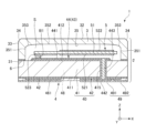
図1に示すように、振動デバイス1は、振動素子5と、振動素子5を収納するパッケージ2と、を有する。また、図2および図3に示すように、パッケージ2は、第1基板として振動素子5を収納する凹部35を有する箱状のリッド3と、第2基板として凹部35の開口を塞いでリッド3と接合された板状のベース4と、を有する。そして、凹部35の開口がベース4で塞がれることにより、振動素子5を収納する収納空間Sが形成される。収納空間Sは、気密であり、減圧状態、好ましくはより真空に近い状態となっている。ただし、収納空間Sの雰囲気は、特に限定されず、例えば、窒素またはAr等の不活性ガスを封入した雰囲気であってもよく、減圧状態でなく大気圧状態または加圧状態となっていてもよい。
As shown in FIG. 1, the
ベース4は、絶縁性を有する基板40と、基板40に配置された電極43と、を有する。さらに、基板40は、ベース基板41と、ベース基板41の表面に配置された絶縁膜42と、を有する。ベース基板41は、平面視形状が矩形の板状であり、互いに表裏関係にある下面411および上面412を有する。また、ベース基板41は、その上面412と下面411とを貫通する2つの貫通孔415、416を有する。
The
ベース基板41の構成材料は、半導体材料である。半導体材料としては、特に限定されず、例えば、シリコン、ゲルマニウムや、GaP、GaAs、InP等の化合物半導体材料を用いることができる。ベース基板41の構成材料として半導体材料を用いることにより、振動デバイス1を半導体プロセスによって形成することができるため、振動デバイス1を精度よく製造することができると共に、その小型化を図ることができる。また、ベース4に、例えば、発振回路等の半導体回路を形成することができ、ベース4を有効活用することができる。特に、本実施形態では、ベース基板41の構成材料として、シリコンを用いている。これにより、入手し易く、安価なベース基板41となる。
The constituent material of the
ただし、ベース基板41の構成材料としては、半導体材料に限定されず、例えば、各種セラミックス材料、各種ガラス材料等を用いることができる。セラミックス材料やガラス材料を用いた場合、ベース基板41自体が絶縁性を有するため、絶縁膜42を省略することができる。
However, the constituent material of the
また、ベース基板41の表面には絶縁膜42が配置されている。ただし、絶縁膜42は、上面412の外縁部すなわちリッド3との接合部には配置されていない。そのため、上面412の外縁部は、絶縁膜42から露出している。絶縁膜42は、シリコン酸化膜(SiO2膜)から構成されている。また、絶縁膜42の形成方法としては、特に限定されず、例えば、ベース基板41の表面を熱酸化することにより形成してもよいし、TEOS(テトラエトキシシラン)を用いたプラズマCVDにより形成してもよい。ただし、絶縁膜42としては、特に限定されず、例えば、ポリイミド等の絶縁性の樹脂材料から構成されていてもよいし、異種材料が積層した複合体で構成されていてもよい。
An insulating
また、絶縁膜42上には電極43が配置されている。電極43は、互いに離間して配置された第1配線44および第2配線45を有する。第1配線44は、基板40の上面に配置され、収納空間S内に臨む内部端子441と、基板40の下面に配置され、パッケージ2の外部に臨む外部端子442と、貫通孔415内に配置され、内部端子441と外部端子442とを電気的に接続する貫通電極443と、を有する。
An
同様に、第2配線45は、基板40の上面に配置され、収納空間S内に臨む内部端子451と、基板40の下面に配置され、パッケージ2の外部に臨む外部端子452と、貫通孔416内に配置され、内部端子451と外部端子452とを電気的に接続する貫通電極453と、を有する。
Similarly, the
また、電極43は、基板40の下面に配置された2つのダミー端子461、462を有する。ダミー端子461、462は、電気的な役割を担っておらず、例えば、パッケージ2と対象物との接合強度を高めるために設けられている。ただし、ダミー端子461、462の役割としては、これに限定されない。
The
リッド3は、下面31(第1主面)と、下面31と表裏関係にある上面32(第2主面)と、下面31と上面32とを接続する外周面33と、上面32と外周面33との間に位置し、上面32および外周面33に対して傾斜している傾斜面34と、を有する。言い換えると、上面32と外周面33の間の角部が面取りされている。これにより、当該部分への応力集中が抑制され、リッド3の機械的強度が高まる。なお、本実施形態では、傾斜面34が平坦面で構成されているが、これに限定されず、曲面で構成されていてもよい。また、本実施形態では、上面32の全周にわたって傾斜面34が形成されているが、これに限定されず、上面32の外周の一部にだけ傾斜面34が形成されていてもよい。また、傾斜面34は、省略してもよい。
The
また、リッド3は、その下面31に開口する有底の凹部35を有する箱状をなす。このようなリッド3の構成材料は、半導体材料である。半導体材料としては、特に限定されず、例えば、シリコン、ゲルマニウムや、GaP、GaAs、InP等の化合物半導体材料を用いることができる。リッド3の構成材料として半導体材料を用いることにより、振動デバイス1を半導体プロセスによって形成することができるため、振動デバイス1を精度よく製造することができると共に、その小型化を図ることができる。特に、本実施形態では、リッド3の構成材料としてシリコンを用いている。これにより、入手し易く、安価なリッド3となる。また、ベース基板41とリッド3の材料を揃えることができ、これらの熱膨張係数差を実質的にゼロとすることができる。そのため、熱膨張に起因する熱応力の発生が抑えられ、優れた振動特性を有する振動デバイス1となる。
The
ただし、リッド3の構成材料としては、半導体材料に限定されず、各種ガラス材料を用いることもできる。リッド3の構成材料として、光透過性を有するガラス材料を用いると、振動デバイス1の製造後に、リッド3を介して振動素子5にレーザーを照射して励振電極522の一部を除去し、振動素子5の周波数調整を行うことができる。
However, the constituent material of the
このようなリッド3は、その下面31において接合部材6を介してベース基板41の上面412と直接接合されている。本実施形態では、直接接合の中でも金属同士の拡散を利用した拡散接合を用いてリッド3とベース基板41とが接合されている。具体的には、リッド3の下面31に金属膜を設けると共に、ベース基板41の上面412に金属膜を設け、これら金属膜同士を拡散接合することにより接合部材6が形成され、この接合部材6を介してリッド3とベース基板41とが接合されている。ただし、接合方法としては、これに限定されず、例えば、リッド3の下面31とベース基板41の上面412とにアルゴンガス等の不活性ガスを照射して、これらの面を活性し、下面31と上面412とを直接接合してもよい。また、樹脂接着剤、低融点ガラス等の各種接合部材を用いて接合してもよい。
The
図4に示すように、振動素子5は、振動基板51と、振動基板51の表面に配置された電極52と、を有する。振動基板51は、厚みすべり振動モードを有し、本実施形態ではATカット水晶基板から形成されている。ATカット水晶基板は、三次の周波数温度特性を有しており、優れた温度特性を有する振動素子5となる。
As shown in FIG. 4 , the vibrating
電極52は、振動基板51の下面に配置された励振電極521と、上面に振動基板51を介して励振電極521と対向して配置された励振電極522と、を有する。また、電極52は、振動基板51の下面に配置された一対の端子523、524と、端子523と励振電極521とを電気的に接続する配線525と、端子524と励振電極522とを電気的に接続する配線526と、を有する。
The
なお、振動素子5の構成は、上述の構成に限定されない。例えば、振動素子5は、励振電極521、522に挟まれた振動領域がその周囲から突出したメサ型となっていてもよいし、逆に、振動領域がその周囲から凹没した逆メサ型となっていてもよい。また、振動基板51の周囲を研削するベベル加工や、上面および下面を凸曲面とするコンベックス加工が施されていてもよい。
Note that the configuration of the
また、振動素子5としては、厚みすべり振動モードで振動するものに限定されず、例えば、2つの振動腕が面内方向に音叉振動する音叉型の振動素子であってもよい。すなわち、振動基板51は、ATカット水晶基板に限定されず、ATカット水晶基板以外の水晶基板、例えば、Xカット水晶基板、Yカット水晶基板、Zカット水晶基板、BTカット水晶基板、SCカット水晶基板、STカット水晶基板等であってもよい。また、本実施形態では、振動基板51が水晶で構成されているが、これに限定されず、例えば、ニオブ酸リチウム、タンタル酸リチウム、四ホウ酸リチウム、ランガライト、ニオブ酸カリウム、リン酸ガリウム等の圧電単結晶体により構成されていてもよいし、これら以外の圧電単結晶体で構成されていてもよい。更にまた、振動素子5は、圧電駆動型の振動素子に限らず、静電気力を用いた静電駆動型の振動素子であってもよい。
Further, the vibrating
このような振動素子5は、図2、図3および図4に示すように、導電性の接合部材B1、B2によってベース4の上面に固定されている。また、接合部材B1は、ベース4が有する内部端子441と振動素子5が有する端子523とを電気的に接続し、接合部材B2は、ベース4が有する内部端子451と振動素子5が有する端子524とを電気的に接続している。
As shown in FIGS. 2, 3 and 4, such a vibrating
接合部材B1、B2としては、導電性と接合性とを兼ね備えていれば、特に限定されず、例えば、金バンプ、銀バンプ、銅バンプ、はんだバンプ等の各種金属バンプ、ポリイミド系、エポキシ系、シリコーン系、アクリル系の各種接着剤に銀フィラー等の導電性フィラーを分散させた導電性接着剤等を用いることができる。接合部材B1、B2として前者の金属バンプを用いると、接合部材B1、B2からのガスの発生を抑制でき、収納空間Sの環境変化、特に圧力の上昇を効果的に抑制することができる。一方、接合部材B1、B2として後者の導電性接着剤を用いると、接合部材B1、B2が金属バンプに比べて柔らかくなり、振動素子5に応力が伝わり難くなる。
The bonding members B1 and B2 are not particularly limited as long as they have both conductivity and bonding properties. A conductive adhesive obtained by dispersing a conductive filler such as a silver filler in various silicone-based or acrylic-based adhesives can be used. When the former metal bumps are used as the bonding members B1 and B2, generation of gas from the bonding members B1 and B2 can be suppressed, and environmental changes in the storage space S, particularly pressure rises, can be effectively suppressed. On the other hand, when the latter conductive adhesive is used as the bonding members B1 and B2, the bonding members B1 and B2 are softer than the metal bumps, and stress is less likely to be transmitted to the vibrating
以上、振動デバイス1の全体構成について簡単に説明した。次に、振動デバイス1の特徴の1つである凹部35の構成について詳細に説明する。図4に示すように、凹部35は、平面視で矩形であり、特に本実施形態では、X軸方向を長手とする長方形である。そのため、図5および図6に示すように、凹部35の内面は、4つの側面351と、底面352と、を有する。そして、凹部35の内面は、さらに、各側面351と底面352との間に位置し、これらを接続する接続面353を有する。接続面353は、断面視で、湾曲凹面からなる曲面である。このように、側面351と底面352との間に曲面からなる接続面353を配置することにより、側面351と底面352との間に角が形成されず、当該部分への応力集中が低減される。したがって、本実施形態のように、機械的強度がそれほど高くないシリコンによってリッド3を構成しても、十分に高い機械的強度を有する振動デバイス1となる。また、応力集中によるクラックが発生し、振動素子5を収納する収納空間Sの気密性が破壊され、振動素子5の周波数等が変動することを抑制できる。
The overall configuration of the
また、側面351と接続面353との境界Qは、振動素子5よりも上側すなわち底面352側に位置している。接続面353が形成されている部分では、接続面353が傾斜している分、収納空間SのX軸方向の幅およびY軸方向の幅が小さくなってしまう。そのため、接続面353を振動素子5よりも上側に配置することにより、振動素子5の配置スペースが小さくなるのを抑制することができ、振動素子5を、リッド3との間に十分なクリアランスを持ってベース4に配置することができる。ただし、これに限定されず、例えば、境界Qは、振動素子5よりも下側に位置していてもよい。
A boundary Q between the
また、接続面353は、リッド3の厚さ方向であるZ軸方向の長さをL1とし、Z軸方向に直交する方向である方向すなわち図5であればX軸方向、図6であればY軸方向の長さをL2としたとき、L2>L1である。これにより、例えば、L2=L1である場合と比べて、応力の分散効率が高まり、リッド3の破損を効果的に抑制することができる。また、L2<L1の場合と比べて、接続面353の高さが抑えられるため、リッド3の小型化を図ることができる。
The
なお、図5および図6に示すように、本実施形態では、接続面353は、その全周においてL2>L1となっているが、少なくとも一部がL2>L1となっていればよい。また、図5と図6とでL2やL1の大きさが異なっていてもよい。この場合は、図5に示すL2、L1がL2>L1であり、図6に示すL2、L1がL2>L1であればよい。
As shown in FIGS. 5 and 6, in the present embodiment, the
また、凹部35の深さをL3としたとき、0.02<L1/L3<0.2である。このように、0.02<L1/L3とすることにより、上述した応力分散効果を十分に発揮することができる。一方、L1/L3<0.2とすることにより、パッケージ2の大型化を効果的に抑制することができる。なお、0.05<L1/L3<0.15であるのがより好ましく、0.07<L1/L3<0.12であるのがさらに好ましい。これにより、上述の効果をより顕著に発揮することができる。ただし、L1とL3との関係は、特に限定されない。
Further, when the depth of the
また、接続面353の側面351側の第1端部P1における曲率半径r1と、底面352側の第2端部P2における曲率半径r2と、中央部P3における曲率半径r3と、を比較すると、r3<r1<r2である。また、第1端部P1と第2端部P2とは、連続した曲面で接続されており、第1端部P1から中央部P3に向けて曲率半径が漸増し、同じく、第2端部P2から中央部P3に向けて曲率半径が漸増している。このように、第1端部P1と第2端部P2とで曲率半径を異ならせることにより、前述した応力分散効果をより顕著に発揮することができる。また、中央部P3の曲率半径r3を、第1、第2端部P1、P2の曲率半径r1、r2よりも小さくすることにより、収納空間Sへの接続面353の張り出しを抑制することができ、収納空間Sの減少を抑制することができる。
Further, when comparing the curvature radius r1 at the first end P1 on the
なお、第1端部P1の曲率半径r1としては、特に限定されないが、例えば、1μm以上、且つ10μm以下であることが好ましく、2μm以上、且つ8μm以下であることがより好ましく、3μm以上、且つ7μm以下であることがさらに好ましい。曲率半径r1をこのような範囲とすることにより、接続面353と側面351とをより滑らかに接続することができる。そのため、接続面353と側面351との境界部への応力の集中を効果的に抑制することができる。一方、第2端部P2の曲率半径r2としては、特に限定されないが、例えば、2×105μm以上、且つ3×105μm以下であることが好ましく、2.2×105μm以上、且つ2.8×105μm以下であることがより好ましく、2.4×105μm以上、且つ2.6×105μm以下であることがさらに好ましい。曲率半径r2をこのような範囲とすることにより、接続面353と底面352とをより滑らかに接続することができる。そのため、接続面353と底面352との境界部への応力の集中を効果的に抑制することができる。
Although the radius of curvature r1 of the first end P1 is not particularly limited, it is preferably 1 μm or more and 10 μm or less, more preferably 2 μm or more and 8 μm or less, 3 μm or more, and It is more preferably 7 μm or less. By setting the curvature radius r1 within such a range, the
また、接続面353のZ軸方向の長さL1としては、特に限定されないが、例えば、6個分のスキャロップSCの高さ以上、14個分のスキャロップSCの高さ以下であることが好ましい。すなわち、1つのスキャロップSCの幅をWとしたとき、6≦L1/W≦14であることが好ましい。これにより、接続面353の長さL1が適度なものとなり、リッド3の大型化を抑制しつつ、前述した応力分散効果を効果的に発揮することができる。ここで、少なくとも2つ以上のスキャロップSCの幅の平均値を幅Wとしてもよいし、最も大きいスキャロップSCの幅を幅Wとしてもよいし、最も小さいスキャロップSCの幅を幅Wとしてもよい。
The length L1 of the
また、側面351と接続面353との境界Qは、側面351の両端部よりも中央部が底面352側に位置している。言い換えると、側面351の両端部での境界Qと底面352との離間距離D1は、側面351の中央部での境界Qと底面352との離間距離D2よりも大きい。つまり、D1>D2である。このように、境界Qの底面352からの距離を側面351の端部と中央部とで異ならせることにより、前述した応力分散効果を効果的に発揮することができ、より機械的強度の高い振動デバイス1となる。特に、本実施形態では、境界Qが底面352側に凸となるように湾曲している。これにより、上述した効果をより顕著に発揮することができる。ただし、これに限定されず、D1≦D2であってもよい。
In addition, the boundary Q between the
ここで、凹部35は、ドライエッチングの一種である「ボッシュ・プロセス」により形成されたエッチング凹部である。ボッシュ・プロセスは、エッチング用ガスであるSF6と、側壁保護膜形成用ガスであるC4F8とを交互に供給することにより、高アスペクト比でシリコンに孔を掘り進める技術であり、その製造上、図7に示すように、側面351には「スキャロップSC」と呼ばれる複数の微小な凹部がZ軸方向に連続して形成される。スキャロップSCの内周面は、曲面であり、この曲率半径r4よりも第1端部P1の曲率半径r1の方が大きい。すなわち、r4<r1である。これにより、接続面353を十分に緩やかな曲面とすることができ、前述した応力分散効果を効果的に発揮することができる。ただし、これに限定されず、r4≧r1であってもよい。
Here, the
以上、振動デバイス1について説明した。このような振動デバイス1は、前述したように、半導体材料またはガラス材料により構成され、第1主面である下面31に開口している凹部35を有する第1基板としてのリッド3と、リッド3の下面31に接合され、凹部35の開口を塞ぐ第2基板としてのベース4と、凹部35に収納される振動素子5と、を備えている。また、凹部35の内面は、側面351、底面352および側面351と底面352とを接続している接続面353を有する。そして、接続面353は、曲面であり、接続面353のリッド3の厚さ方向である第1方向としてのZ軸方向の長さをL1とし、Z軸方向に直交する第2方向としてのX-Y面内方向の長さをL2としたとき、L1<L2である。このように、側面351と底面352との間に曲面からなる接続面353を配置することにより、側面351と底面352との間に角が形成されず、当該部分への応力集中が低減される。したがって、本実施形態のように、機械的強度がそれほど高くないシリコンによってリッド3を構成しても、十分に高い機械的強度を有する振動デバイス1となる。
The
また、前述したように、凹部35のZ軸方向の深さをL3としたとき、0.02<L1/L3<0.2である。このように、0.02<L1/L3とすることにより、上述した応力分散効果を十分に発揮することができる。一方、L1/L3<0.2とすることにより、パッケージ2の大型化を効果的に抑制することができる。
As described above, 0.02<L1/L3<0.2, where L3 is the depth of the
また、前述したように、凹部35は、平面視で矩形であり、凹部35の内面は、4つの側面351を有する。そして、側面351と接続面353との境界Qは、側面351の両端部よりも中央部が底面352側に位置している。このように、境界Qの底面352からの距離を側面351の端部と中央部とで異ならせることにより、前述した応力分散効果を効果的に発揮することができ、より機械的強度の高い振動デバイス1となる。特に、本実施形態では、境界Qが底面352側に凸となるように湾曲している。これにより、上述した効果をより顕著に発揮することができる。
Further, as described above, the
また、前述したように、側面351と接続面353との境界Qは、振動素子5よりも底面352側に位置している。これにより、振動素子5の配置スペースが小さくなるのを抑制することができ、振動素子5を、リッド3との間に十分なクリアランスを持ってベース4に配置することができる。
Further, as described above, the boundary Q between the
また、前述したように、リッド3は、下面31と表裏関係にある第2主面としての上面32と、下面31と上面32とを接続する外周面33と、上面32と外周面33との間に位置し、上面32および外周面33に対して傾斜している傾斜面34と、を有する。言い換えると、上面32と外周面33の間の角部が面取りされている。これにより、当該部分への応力集中が抑制され、リッド3の機械的強度が高まる。
In addition, as described above, the
また、前述したように、接続面353の側面351側の第1端部P1における曲率半径r1は、1μm以上、且つ10μm以下であり、接続面353の底面352側の第2端部P2における曲率半径r2は、2×105μm以上、且つ3×105μm以下である。また、第1端部P1と第2端部P2との間は、連続的な曲面である。これにより、接続面353によって、側面351と底面352とをより滑らかに接続することができる。そのため、接続面353への応力集中はもちろんのこと、接続面353と側面351との境界部や接続面353と底面352との境界部への応力集中についても効果的に抑制することができる。
Further, as described above, the curvature radius r1 at the first end P1 on the
また、前述したように、凹部35は、ドライエッチングにより形成されたエッチング凹部であり、側面351は、ドライエッチングにより形成された複数のスキャロップSCを有する。そして、第1端部P1における接続面353の曲率半径r1は、スキャロップSCの曲率半径r4よりも大きい。つまり、r4<r1である。これにより、接続面353を十分に緩やかな曲面とすることができ、前述した応力分散効果を効果的に発揮することができる。
Further, as described above, the
<第2実施形態>
図8は、第2実施形態に係る発振器を示す断面図である。なお、図8は、図2に相当する断面図である。
<Second embodiment>
FIG. 8 is a cross-sectional view showing the oscillator according to the second embodiment. 8 is a cross-sectional view corresponding to FIG.
本実施形態に係る発振器10は、ベース4に発振回路48が形成されていること以外は、前述した第1実施形態の振動デバイス1と同様である。なお、以下の説明では、第2実施形態の振動デバイス1に関し、前述した第1実施形態との相違点を中心に説明し、同様の事項に関してはその説明を省略する。また、図8では、前述した実施形態と同様の構成について、同一符号を付している。
The
図8に示す発振器10は、ベース4に形成され、振動素子5と電気的に接続された発振回路48を有する。本実施形態では、ベース基板41の下面411が能動面となっている。また、ベース基板41の下面411には、絶縁層491と配線層492とが積層した積層体49が設けられ、この配線層492を介して下面411に形成された複数の図示しない回路要素が電気的に接続され、発振回路48が構成されている。このように、ベース4に発振回路48を形成することにより、ベース4のスペースを有効活用することができる。
The
このように、発振器10は、振動デバイス1と、振動素子5と電気的に接続され、振動素子5を発振させる発振回路48と、を有する。そのため、発振器10は、前述した振動デバイス1の効果を享受でき、高い信頼性を発揮することができる。
Thus, the
なお、本実施形態では、ベース基板41の下面411が能動面となっているが、これに限定されず、ベース基板41の上面412が能動面となっていてもよい。ベース基板41の上面412を能動面とすることで、振動素子5と発振回路48との電気的な接続をより低インピーダンスにすることが可能となり、発振器のより安定した発振が可能となる。また、発振回路48は、ベース4と別体で形成されていてもよい。この場合、発振回路48は、収納空間S内に配置されていてもよいし、収納空間S外に配置されていてもよい。
Although the
<第3実施形態>
図9は、第3実施形態に係る振動モジュールを示す断面図である。
<Third Embodiment>
FIG. 9 is a cross-sectional view showing a vibration module according to the third embodiment.
図9に示す振動モジュール1000は、支持基板1010と、支持基板1010に搭載された回路基板1020と、回路基板1020に搭載された振動デバイス1と、回路基板1020および振動デバイス1をモールドするモールド材Mと、を有する。
A
支持基板1010は、例えば、インターポーザー基板である。支持基板1010の上面には複数の接続端子1011が配置され、下面には複数の実装端子1012が配置されている。また、支持基板1010内には図示しない内部配線が配置され、この内部配線を介して、各接続端子1011が、対応する実装端子1012と電気的に接続されている。このような支持基板1010としては、特に限定されず、例えば、シリコン基板、セラミック基板、樹脂基板、ガラス基板、ガラスエポキシ基板等を用いることができる。
また、回路基板1020は、ダイアタッチ材を介して支持基板1010の上面に接合されている。回路基板1020には、振動デバイス1が有する振動素子5を発振させてクロック信号等の基準信号の周波数を生成する発振回路1023が形成されており、その上面に発振回路1023と電気的に接続された複数の端子1022が配置されている。そして、一部の端子1022は、ボンディングワイヤーBWを介して接続端子1011と電気的に接続されており、一部の端子1022は、例えば、導電性の接合部材B3を介して振動デバイス1と電気的に接続されている。
Also, the
モールド材Mは、回路基板1020および振動デバイス1をモールドし、水分、埃、衝撃等から保護している。モールド材Mとしては、特に限定されないが、例えば、熱硬化型のエポキシ樹脂を用いることができ、トランスファーモールド法によってモールドすることができる。
The molding material M molds the
このように、振動モジュール1000は、振動デバイス1と、振動デバイス1が搭載されているモジュール部品としての回路基板1020と、振動デバイス1を覆うモールド材Mと、を有する。そのため、振動モジュール1000は、前述した振動デバイス1の効果を享受でき、優れた信頼性を発揮することができる。特に、前述したように、振動デバイス1では、リッド3の凹部35に接続面353を形成すると共に、リッド3の外周に傾斜面34を形成し、応力を効果的に分散できる構成となっている。そのため、モールド中に加わる応力による振動デバイス1の破損を効果的に抑制することができる。
Thus, the
<第4実施形態>
図10は、第4実施形態に係るパーソナルコンピューターを示す斜視図である。
<Fourth Embodiment>
FIG. 10 is a perspective view showing a personal computer according to the fourth embodiment.
図10に示す電子機器としてのパーソナルコンピューター1100は、キーボード1102を備えた本体部1104と、表示部1108を備えた表示ユニット1106とにより構成され、表示ユニット1106は、本体部1104に対しヒンジ構造部を介して回動可能に支持されている。このようなパーソナルコンピューター1100には、発振器10が内蔵されている。また、パーソナルコンピューター1100は、キーボード1102や表示部1108などの制御に関する演算処理を行う演算処理回路1110を備えている。演算処理回路1110は、発振器10から出力される発振信号に基づいて動作する。
A
このように、電子機器としてのパーソナルコンピューター1100は、発振器10と、発振器10から出力される発振信号に基づいて動作する演算処理回路1110と、を備える。そのため、前述した発振器10の効果を享受でき、高い信頼性を発揮することができる。
As described above, the
<第5実施形態>
図11は、第5実施形態に係る携帯電話機を示す斜視図である。
<Fifth Embodiment>
FIG. 11 is a perspective view showing a mobile phone according to the fifth embodiment.
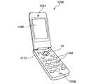
図11に示す電子機器としての携帯電話機1200は、図示しないアンテナ、複数の操作ボタン1202、受話口1204および送話口1206を備え、操作ボタン1202と受話口1204との間には表示部1208が配置されている。このような携帯電話機1200には、発振器10が内蔵されている。また、携帯電話機1200は、操作ボタン1202などの制御に関する演算処理を行う演算処理回路1210を備えている。演算処理回路1210は、発振器10から出力される発振信号に基づいて動作する。
A
このように、電子機器としての携帯電話機1200は、発振器10と、発振器10から出力される発振信号に基づいて動作する演算処理回路1210と、を備える。そのため、前述した発振器10の効果を享受でき、高い信頼性を発揮することができる。
As described above, the
<第6実施形態>
図12は、第6実施形態に係るデジタルスチールカメラを示す斜視図である。
<Sixth Embodiment>
FIG. 12 is a perspective view showing a digital still camera according to the sixth embodiment.
図12に示すデジタルスチールカメラ1300は、ボディ1302を有し、ボディ1302の背面にはCCDによる撮像信号に基づいて表示を行う表示部1310が設けられている。表示部1310は、被写体を電子画像として表示するファインダーとして機能する。また、ボディ1302の正面側(図中裏面側)には、光学レンズやCCDなどを含む受光ユニット1304が設けられている。そして、撮影者が表示部1310に表示された被写体像を確認し、シャッターボタン1306を押すと、その時点におけるCCDの撮像信号が、メモリー1308に転送・格納される。このようなデジタルスチールカメラ1300には、例えば、発振器10が内蔵されている。また、デジタルスチールカメラ1300は、表示部1310や受光ユニット1304などの制御に関する演算処理を行う演算処理回路1312を備えている。演算処理回路1312は、発振器10から出力される発振信号に基づいて動作する。
A
このように、電子機器としてのデジタルスチールカメラ1300は、発振器10と、発振器10から出力される発振信号に基づいて動作する演算処理回路1312と、を備える。そのため、前述した発振器10の効果を享受でき、高い信頼性を発揮することができる。
As described above, the
なお、本適用例の電子機器は、前述したパーソナルコンピューター、携帯電話機およびデジタルスチールカメラの他にも、例えば、スマートフォン、タブレット端末、時計(スマートウォッチを含む)、インクジェット式吐出装置(例えばインクジェットプリンタ)、ラップトップ型パーソナルコンピューター、テレビ、HMD(ヘッドマウントディスプレイ)等のウェアラブル端末、ビデオカメラ、ビデオテープレコーダー、カーナビゲーション装置、ページャ、電子手帳(通信機能付も含む)、電子辞書、電卓、電子ゲーム機器、ワードプロセッサー、ワークステーション、テレビ電話、防犯用テレビモニター、電子双眼鏡、POS端末、医療機器(例えば電子体温計、血圧計、血糖計、心電図計測装置、超音波診断装置、電子内視鏡)、魚群探知機、各種測定機器、移動体端末基地局用機器、計器類(例えば、車両、航空機、船舶の計器類)、フライトシミュレーター、ネットワークサーバー等に適用することができる。 In addition to the personal computers, mobile phones, and digital still cameras described above, the electronic devices of this application example include, for example, smartphones, tablet terminals, watches (including smart watches), and inkjet ejection devices (eg, inkjet printers). , laptop personal computers, televisions, wearable terminals such as HMDs (head-mounted displays), video cameras, video tape recorders, car navigation devices, pagers, electronic notebooks (including those with communication functions), electronic dictionaries, calculators, electronic games Equipment, word processors, workstations, videophones, security TV monitors, electronic binoculars, POS terminals, medical equipment (e.g., electronic thermometers, blood pressure monitors, blood glucose meters, electrocardiogram measuring devices, ultrasonic diagnostic devices, electronic endoscopes), schools of fish It can be applied to detectors, various measuring devices, equipment for mobile terminal base stations, instruments (for example, instruments for vehicles, aircraft, and ships), flight simulators, network servers, and the like.
<第7実施形態>
図13は、第7実施形態に係る自動車を示す斜視図である。
<Seventh embodiment>
FIG. 13 is a perspective view showing an automobile according to the seventh embodiment.
図13に示す自動車1500には、発振器10と、発振器10から出力される発振信号に基づいて動作する演算処理回路1510が内蔵されている。そのような発振器10と演算処理回路1510は、例えば、キーレスエントリー、イモビライザー、カーナビゲーションシステム、カーエアコン、アンチロックブレーキシステム(ABS)、エアバック、タイヤ・プレッシャー・モニタリング・システム(TPMS:Tire Pressure Monitoring System)、エンジンコントロール、ハイブリッド自動車や電気自動車の電池モニター、車体姿勢制御システム等の電子制御ユニット(ECU:electronic control unit)に広く適用できる。
An
このように、移動体としての自動車1500は、発振器10と、発振器10から出力される発振信号に基づいて動作する演算処理回路1510と、を備える。そのため、前述した発振器10の効果を享受でき、高い信頼性を発揮することができる。
Thus,
なお、移動体としては、自動車1500に限定されず、例えば、飛行機、船舶、AGV(無人搬送車)、二足歩行ロボット、ドローン等の無人飛行機等にも適用することができる。
The mobile object is not limited to the
以上、本適用例の振動デバイス、発振器、振動モジュール、電子機器および移動体を図示の実施形態に基づいて説明したが、本適用例は、これに限定されるものではなく、各部の構成は、同様の機能を有する任意の構成のものに置換することができる。また、本適用例に、他の任意の構成物が付加されていてもよい。また、本適用例は、前記各実施形態のうちの、任意の2以上の構成を組み合わせたものであってもよい。 The vibration device, the oscillator, the vibration module, the electronic device, and the moving object of this application example have been described above based on the illustrated embodiments, but this application example is not limited to this, and the configuration of each part is as follows. Any configuration having a similar function can be substituted. In addition, other arbitrary components may be added to this application example. Further, this application example may be a combination of any two or more configurations of the above embodiments.
1…振動デバイス、10…発振器、2…パッケージ、3…リッド、31…下面、32…上面、33…外周面、34…傾斜面、35…凹部、351…側面、352…底面、353…接続面、4…ベース、40…基板、41…ベース基板、411…下面、412…上面、415、416…貫通孔、42…絶縁膜、43…電極、44…第1配線、441…内部端子、442…外部端子、443…貫通電極、45…第2配線、451…内部端子、452…外部端子、453…貫通電極、461…ダミー端子、462…ダミー端子、48…発振回路、49…積層体、491…絶縁層、492…配線層、5…振動素子、51…振動基板、52…電極、521、522…励振電極、523、524…端子、525、526…配線、6…接合部材、1000…振動モジュール、1010…支持基板、1011…接続端子、1012…実装端子、1020…回路基板、1022…端子、1023…発振回路、1100…パーソナルコンピューター、1102…キーボード、1104…本体部、1106…表示ユニット、1108…表示部、1110…演算処理回路、1200…携帯電話機、1202…操作ボタン、1204…受話口、1206…送話口、1208…表示部、1210…演算処理回路、1300…デジタルスチールカメラ、1302…ボディ、1304…受光ユニット、1306…シャッターボタン、1308…メモリー、1310…表示部、1312…演算処理回路、1500…自動車、1510…演算処理回路、B1…接合部材、B2…接合部材、B3…接合部材、BW…ボンディングワイヤー、D1…離間距離、D2…離間距離、L1、L2…長さ、L3…深さ、M…モールド材、P1…第1端部、P2…第2端部、P3…中央部、Q…境界、S…収納空間、SC…スキャロップ
DESCRIPTION OF
Claims (11)
前記第1主面に接合され、前記凹部の開口を塞ぐ第2基板と、
前記凹部に収納される振動素子と、を備え、
前記凹部の内面は、側面、底面および前記側面と前記底面とを接続している接続面を有し、
前記接続面は、曲面であり、
前記接続面の前記第1基板の厚さ方向である第1方向の長さをL1とし、前記第1方向に直交する第2方向の長さをL2としたとき、
L1<L2であることを特徴とする振動デバイス。 a first substrate made of a semiconductor material or a glass material and having a recess opening in the first main surface;
a second substrate that is bonded to the first main surface and closes the opening of the recess;
a vibrating element housed in the recess,
The inner surface of the recess has a side surface, a bottom surface, and a connection surface connecting the side surface and the bottom surface,
The connection surface is a curved surface,
When the length of the connecting surface in the first direction, which is the thickness direction of the first substrate, is L1, and the length in the second direction perpendicular to the first direction is L2,
A vibrating device characterized in that L1<L2.
0.02<L1/L3<0.2である請求項1に記載の振動デバイス。 When the depth of the recess in the first direction is L3,
2. The vibrating device according to claim 1, wherein 0.02<L1/L3<0.2.
前記凹部の内面は、4つの前記側面を有し、
前記側面と前記接続面との境界は、前記側面の両端部よりも中央部が前記底面側に位置している請求項1または2に記載の振動デバイス。 The recess is rectangular in plan view,
The inner surface of the recess has the four side surfaces,
3. The vibrating device according to claim 1, wherein a boundary between the side surface and the connection surface is located closer to the bottom surface than both end portions of the side surface.
前記接続面の前記底面側の第2端部における曲率半径は、2×105μm以上、且つ3×105μm以下であり、
前記第1端部と前記第2端部との間は、連続的な曲面である請求項1ないし5のいずれか1項に記載の振動デバイス。 a radius of curvature of the connection surface at the first end on the side surface side is 1 μm or more and 10 μm or less;
a radius of curvature of the second end of the connection surface on the bottom surface side is 2×10 5 μm or more and 3×10 5 μm or less;
6. The vibration device according to any one of claims 1 to 5, wherein a continuous curved surface is provided between the first end and the second end.
前記側面は、前記ドライエッチングにより形成された複数のスキャロップを有し、
前記第1端部における前記接続面の曲率半径は、前記スキャロップの曲率半径よりも大きい請求項6に記載の振動デバイス。 The recess is an etching recess formed by dry etching,
The side surface has a plurality of scallops formed by the dry etching,
7. The vibration device according to claim 6, wherein the radius of curvature of the connecting surface at the first end is greater than the radius of curvature of the scallops.
前記振動素子と電気的に接続され、前記振動素子を発振させる発振回路と、を有することを特徴とする発振器。 a vibration device according to any one of claims 1 to 7;
an oscillator circuit electrically connected to the vibrating element to cause the vibrating element to oscillate.
前記振動デバイスが搭載されているモジュール部品と、
前記振動デバイスを覆うモールド材と、を有することを特徴とする振動モジュール。 a vibration device according to any one of claims 1 to 7;
a module component on which the vibration device is mounted;
and a molding material covering the vibration device.
前記発振器から出力される発振信号に基づいて動作する演算処理回路と、を備えていることを特徴とする電子機器。 an oscillator according to claim 8;
and an arithmetic processing circuit that operates based on the oscillation signal output from the oscillator.
前記発振器から出力される発振信号に基づいて動作する演算処理回路と、を備えていることを特徴とする移動体。 an oscillator according to claim 8;
and an arithmetic processing circuit that operates based on the oscillation signal output from the oscillator.
Priority Applications (2)
| Application Number | Priority Date | Filing Date | Title |
|---|---|---|---|
| JP2019057427A JP7247694B2 (en) | 2019-03-25 | 2019-03-25 | Vibration devices, oscillators, vibration modules, electronic devices and moving objects |
| US16/828,631 US11653571B2 (en) | 2019-03-25 | 2020-03-24 | Resonance device, oscillator, resonance module, electronic device and vehicle |
Applications Claiming Priority (1)
| Application Number | Priority Date | Filing Date | Title |
|---|---|---|---|
| JP2019057427A JP7247694B2 (en) | 2019-03-25 | 2019-03-25 | Vibration devices, oscillators, vibration modules, electronic devices and moving objects |
Publications (3)
| Publication Number | Publication Date |
|---|---|
| JP2020161907A JP2020161907A (en) | 2020-10-01 |
| JP2020161907A5 JP2020161907A5 (en) | 2022-02-01 |
| JP7247694B2 true JP7247694B2 (en) | 2023-03-29 |
Family
ID=72604864
Family Applications (1)
| Application Number | Title | Priority Date | Filing Date |
|---|---|---|---|
| JP2019057427A Active JP7247694B2 (en) | 2019-03-25 | 2019-03-25 | Vibration devices, oscillators, vibration modules, electronic devices and moving objects |
Country Status (2)
| Country | Link |
|---|---|
| US (1) | US11653571B2 (en) |
| JP (1) | JP7247694B2 (en) |
Citations (13)
| Publication number | Priority date | Publication date | Assignee | Title |
|---|---|---|---|---|
| JP2004079467A (en) | 2002-08-22 | 2004-03-11 | Nippon Sheet Glass Co Ltd | Sealing plate for el element, and mother glass substrate for forming multiple sealing plate |
| JP2006295246A (en) | 2005-04-05 | 2006-10-26 | Matsushita Electric Ind Co Ltd | Electronic component and manufacturing method thereof |
| JP2009027477A (en) | 2007-07-19 | 2009-02-05 | Citizen Finetech Miyota Co Ltd | Piezoelectric oscillator |
| JP2010166346A (en) | 2009-01-16 | 2010-07-29 | Epson Toyocom Corp | Temperature-controlled piezoelectric oscillator |
| JP2012030865A (en) | 2010-07-30 | 2012-02-16 | Yoshino Kogyosho Co Ltd | Synthetic resin cup vessel |
| JP2012212797A (en) | 2011-03-31 | 2012-11-01 | Dainippon Printing Co Ltd | Semiconductor device manufacturing method |
| JP2013165100A (en) | 2012-02-09 | 2013-08-22 | Seiko Epson Corp | Semiconductor device, semiconductor device manufacturing method, circuit device and electronic apparatus |
| WO2013172442A1 (en) | 2012-05-18 | 2013-11-21 | 株式会社村田製作所 | Crystal oscillator |
| JP2014150363A (en) | 2013-01-31 | 2014-08-21 | Asahi Kasei Electronics Co Ltd | Piezoelectric device and method for manufacturing the same |
| US20150022988A1 (en) | 2013-07-16 | 2015-01-22 | Seiko Instruments Inc. | Lid body portion and electronic device package using the lid body portion and electronic device |
| WO2016199918A1 (en) | 2015-06-12 | 2016-12-15 | 株式会社村田製作所 | Crystal piece and crystal oscillator |
| JP2017120865A (en) | 2015-12-29 | 2017-07-06 | 日立金属株式会社 | Hermetic sealing cap |
| JP2018098599A (en) | 2016-12-12 | 2018-06-21 | 株式会社村田製作所 | Piezoelectric vibrator, module component, and manufacturing methods of piezoelectric vibrator and module component |
Family Cites Families (14)
| Publication number | Priority date | Publication date | Assignee | Title |
|---|---|---|---|---|
| JPH04284006A (en) | 1991-03-13 | 1992-10-08 | Seiko Epson Corp | Piezoelectric oscillator |
| JPH05206307A (en) | 1992-01-24 | 1993-08-13 | Toshiba Corp | Semiconductor device |
| JPH10264922A (en) * | 1997-03-25 | 1998-10-06 | Idemitsu Petrochem Co Ltd | Synthetic resin container |
| US6726372B1 (en) * | 2000-04-06 | 2004-04-27 | Shipley±Company, L.L.C. | 2-Dimensional optical fiber array made from etched sticks having notches |
| JP2009017454A (en) * | 2007-07-09 | 2009-01-22 | Kyocera Kinseki Corp | Piezoelectric vibrator and method of manufacturing the same |
| JP5213614B2 (en) | 2008-09-26 | 2013-06-19 | シチズンファインテックミヨタ株式会社 | Piezoelectric device and manufacturing method thereof |
| JP5428735B2 (en) | 2009-10-14 | 2014-02-26 | セイコーエプソン株式会社 | Piezoelectric device |
| JP5129284B2 (en) | 2010-03-09 | 2013-01-30 | 日本電波工業株式会社 | Piezoelectric vibrator and method for manufacturing the piezoelectric vibrator |
| JP5599057B2 (en) | 2010-09-30 | 2014-10-01 | セイコーインスツル株式会社 | Package and piezoelectric vibrator |
| JP5817158B2 (en) * | 2011-03-16 | 2015-11-18 | セイコーエプソン株式会社 | Optical device, optical device manufacturing method, optical scanner, and image forming apparatus |
| CN103748787B (en) | 2011-08-22 | 2017-04-12 | 京瓷株式会社 | Elastic wave device and electronic component |
| JP2013074517A (en) | 2011-09-28 | 2013-04-22 | Seiko Instruments Inc | Method of manufacturing package, piezoelectric vibrator, oscillator, electronic apparatus, and electric wave clock |
| US9620702B2 (en) * | 2011-09-30 | 2017-04-11 | Daishinku Corporation | Electronic component package, electronic component package sealing member and method for producing the electronic component package sealing member |
| JP6295611B2 (en) * | 2013-11-05 | 2018-03-20 | セイコーエプソン株式会社 | Vibrator, oscillator, electronic device, and moving object |
-
2019
- 2019-03-25 JP JP2019057427A patent/JP7247694B2/en active Active
-
2020
- 2020-03-24 US US16/828,631 patent/US11653571B2/en active Active
Patent Citations (14)
| Publication number | Priority date | Publication date | Assignee | Title |
|---|---|---|---|---|
| JP2004079467A (en) | 2002-08-22 | 2004-03-11 | Nippon Sheet Glass Co Ltd | Sealing plate for el element, and mother glass substrate for forming multiple sealing plate |
| JP2006295246A (en) | 2005-04-05 | 2006-10-26 | Matsushita Electric Ind Co Ltd | Electronic component and manufacturing method thereof |
| JP2009027477A (en) | 2007-07-19 | 2009-02-05 | Citizen Finetech Miyota Co Ltd | Piezoelectric oscillator |
| JP2010166346A (en) | 2009-01-16 | 2010-07-29 | Epson Toyocom Corp | Temperature-controlled piezoelectric oscillator |
| JP2012030865A (en) | 2010-07-30 | 2012-02-16 | Yoshino Kogyosho Co Ltd | Synthetic resin cup vessel |
| JP2012212797A (en) | 2011-03-31 | 2012-11-01 | Dainippon Printing Co Ltd | Semiconductor device manufacturing method |
| JP2013165100A (en) | 2012-02-09 | 2013-08-22 | Seiko Epson Corp | Semiconductor device, semiconductor device manufacturing method, circuit device and electronic apparatus |
| WO2013172442A1 (en) | 2012-05-18 | 2013-11-21 | 株式会社村田製作所 | Crystal oscillator |
| JP2014150363A (en) | 2013-01-31 | 2014-08-21 | Asahi Kasei Electronics Co Ltd | Piezoelectric device and method for manufacturing the same |
| US20150022988A1 (en) | 2013-07-16 | 2015-01-22 | Seiko Instruments Inc. | Lid body portion and electronic device package using the lid body portion and electronic device |
| JP2015023052A (en) | 2013-07-16 | 2015-02-02 | セイコーインスツル株式会社 | Lid body part, package for electronic device using this lid body part, and electronic device |
| WO2016199918A1 (en) | 2015-06-12 | 2016-12-15 | 株式会社村田製作所 | Crystal piece and crystal oscillator |
| JP2017120865A (en) | 2015-12-29 | 2017-07-06 | 日立金属株式会社 | Hermetic sealing cap |
| JP2018098599A (en) | 2016-12-12 | 2018-06-21 | 株式会社村田製作所 | Piezoelectric vibrator, module component, and manufacturing methods of piezoelectric vibrator and module component |
Also Published As
| Publication number | Publication date |
|---|---|
| US20200313070A1 (en) | 2020-10-01 |
| US11653571B2 (en) | 2023-05-16 |
| JP2020161907A (en) | 2020-10-01 |
Similar Documents
| Publication | Publication Date | Title |
|---|---|---|
| US11075613B2 (en) | Vibrator device, electronic apparatus, and vehicle | |
| JP2023065527A (en) | Vibration device, vibration module, and electronic apparatus | |
| JP7314562B2 (en) | Vibration devices, oscillators, electronic devices and moving objects | |
| JP2016072937A (en) | Vibrator, oscillator, electronic apparatus and movable body | |
| JP7247694B2 (en) | Vibration devices, oscillators, vibration modules, electronic devices and moving objects | |
| JP7230541B2 (en) | Vibration device and vibration module | |
| US11097667B2 (en) | Vibration device, vibration module, electronic apparatus, and vehicle | |
| US11183986B2 (en) | Resonator element, resonator device, electronic apparatus, and vehicle | |
| JP2020123881A (en) | Vibration device, vibration module, electronic apparatus, and movable body | |
| JP7200705B2 (en) | Vibration device, manufacturing method of vibration device, vibration module, electronic device, and moving body | |
| JP2020108087A (en) | Vibration device, electronic apparatus, and movable body | |
| JP7367311B2 (en) | Vibration elements, vibration devices, oscillators, electronic equipment and moving objects | |
| JP2019176224A (en) | Vibrator, oscillator, electronic apparatus, and movable body | |
| JP2015050483A (en) | Electronic device, electronic apparatus, and mobile | |
| JP2019145978A (en) | Vibration element, vibrator, oscillator, electronic apparatus, and movable body | |
| JP2019022140A (en) | Vibrating device, manufacturing method of vibration device, oscillator, electronic device, and moving body | |
| JP7211081B2 (en) | vibration device | |
| JP2021175056A (en) | Vibration device, vibration module, electronic apparatus, and movable body | |
| JP2020123926A (en) | Vibration device, vibration module, electronic device, moving body, and manufacturing method of vibration device | |
| JP2019169796A (en) | Vibration device, electronic apparatus, and movable body |
Legal Events
| Date | Code | Title | Description |
|---|---|---|---|
| A521 | Request for written amendment filed |
Free format text: JAPANESE INTERMEDIATE CODE: A523 Effective date: 20220124 |
|
| A621 | Written request for application examination |
Free format text: JAPANESE INTERMEDIATE CODE: A621 Effective date: 20220124 |
|
| A977 | Report on retrieval |
Free format text: JAPANESE INTERMEDIATE CODE: A971007 Effective date: 20230130 |
|
| TRDD | Decision of grant or rejection written | ||
| A01 | Written decision to grant a patent or to grant a registration (utility model) |
Free format text: JAPANESE INTERMEDIATE CODE: A01 Effective date: 20230214 |
|
| A61 | First payment of annual fees (during grant procedure) |
Free format text: JAPANESE INTERMEDIATE CODE: A61 Effective date: 20230227 |
|
| R150 | Certificate of patent or registration of utility model |
Ref document number: 7247694 Country of ref document: JP Free format text: JAPANESE INTERMEDIATE CODE: R150 |