JP2020123881A - Vibration device, vibration module, electronic apparatus, and movable body - Google Patents
Vibration device, vibration module, electronic apparatus, and movable body Download PDFInfo
- Publication number
- JP2020123881A JP2020123881A JP2019015322A JP2019015322A JP2020123881A JP 2020123881 A JP2020123881 A JP 2020123881A JP 2019015322 A JP2019015322 A JP 2019015322A JP 2019015322 A JP2019015322 A JP 2019015322A JP 2020123881 A JP2020123881 A JP 2020123881A
- Authority
- JP
- Japan
- Prior art keywords
- substrate
- joining member
- region
- vibrating
- virtual line
- Prior art date
- Legal status (The legal status is an assumption and is not a legal conclusion. Google has not performed a legal analysis and makes no representation as to the accuracy of the status listed.)
- Pending
Links
- 239000000758 substrate Substances 0.000 claims abstract description 121
- 230000005284 excitation Effects 0.000 claims abstract description 42
- 230000005484 gravity Effects 0.000 claims abstract description 7
- VYPSYNLAJGMNEJ-UHFFFAOYSA-N silicon dioxide Inorganic materials O=[Si]=O VYPSYNLAJGMNEJ-UHFFFAOYSA-N 0.000 claims description 18
- 239000010453 quartz Substances 0.000 claims description 17
- XUIMIQQOPSSXEZ-UHFFFAOYSA-N Silicon Chemical compound [Si] XUIMIQQOPSSXEZ-UHFFFAOYSA-N 0.000 claims description 14
- 229910052710 silicon Inorganic materials 0.000 claims description 14
- 239000010703 silicon Substances 0.000 claims description 14
- 239000013078 crystal Substances 0.000 abstract description 30
- 230000035882 stress Effects 0.000 description 21
- 230000000694 effects Effects 0.000 description 15
- 239000004065 semiconductor Substances 0.000 description 13
- 239000011521 glass Substances 0.000 description 7
- 239000002184 metal Substances 0.000 description 7
- 229910052751 metal Inorganic materials 0.000 description 7
- 230000035945 sensitivity Effects 0.000 description 6
- 239000000919 ceramic Substances 0.000 description 5
- 239000000463 material Substances 0.000 description 5
- 238000000034 method Methods 0.000 description 5
- 238000012986 modification Methods 0.000 description 5
- 230000004048 modification Effects 0.000 description 5
- 230000010355 oscillation Effects 0.000 description 5
- 230000008646 thermal stress Effects 0.000 description 5
- 239000000853 adhesive Substances 0.000 description 4
- 230000001070 adhesive effect Effects 0.000 description 4
- 239000004593 Epoxy Substances 0.000 description 3
- 238000009792 diffusion process Methods 0.000 description 3
- 230000006870 function Effects 0.000 description 3
- WABPQHHGFIMREM-UHFFFAOYSA-N lead(0) Chemical compound [Pb] WABPQHHGFIMREM-UHFFFAOYSA-N 0.000 description 3
- 239000012778 molding material Substances 0.000 description 3
- 229920005989 resin Polymers 0.000 description 3
- 239000011347 resin Substances 0.000 description 3
- XKRFYHLGVUSROY-UHFFFAOYSA-N Argon Chemical compound [Ar] XKRFYHLGVUSROY-UHFFFAOYSA-N 0.000 description 2
- IJGRMHOSHXDMSA-UHFFFAOYSA-N Atomic nitrogen Chemical compound N#N IJGRMHOSHXDMSA-UHFFFAOYSA-N 0.000 description 2
- 229910001218 Gallium arsenide Inorganic materials 0.000 description 2
- 239000004642 Polyimide Substances 0.000 description 2
- BQCADISMDOOEFD-UHFFFAOYSA-N Silver Chemical compound [Ag] BQCADISMDOOEFD-UHFFFAOYSA-N 0.000 description 2
- BOTDANWDWHJENH-UHFFFAOYSA-N Tetraethyl orthosilicate Chemical compound CCO[Si](OCC)(OCC)OCC BOTDANWDWHJENH-UHFFFAOYSA-N 0.000 description 2
- 150000001875 compounds Chemical class 0.000 description 2
- 238000000605 extraction Methods 0.000 description 2
- 239000007789 gas Substances 0.000 description 2
- 229910052732 germanium Inorganic materials 0.000 description 2
- GNPVGFCGXDBREM-UHFFFAOYSA-N germanium atom Chemical compound [Ge] GNPVGFCGXDBREM-UHFFFAOYSA-N 0.000 description 2
- 239000011261 inert gas Substances 0.000 description 2
- 238000000465 moulding Methods 0.000 description 2
- 230000003287 optical effect Effects 0.000 description 2
- 229920001721 polyimide Polymers 0.000 description 2
- 238000012545 processing Methods 0.000 description 2
- 229910052709 silver Inorganic materials 0.000 description 2
- 239000004332 silver Substances 0.000 description 2
- 229910000679 solder Inorganic materials 0.000 description 2
- 241000251468 Actinopterygii Species 0.000 description 1
- RYGMFSIKBFXOCR-UHFFFAOYSA-N Copper Chemical compound [Cu] RYGMFSIKBFXOCR-UHFFFAOYSA-N 0.000 description 1
- WQZGKKKJIJFFOK-GASJEMHNSA-N Glucose Natural products OC[C@H]1OC(O)[C@H](O)[C@@H](O)[C@@H]1O WQZGKKKJIJFFOK-GASJEMHNSA-N 0.000 description 1
- 229910004298 SiO 2 Inorganic materials 0.000 description 1
- NIXOWILDQLNWCW-UHFFFAOYSA-N acrylic acid group Chemical group C(C=C)(=O)O NIXOWILDQLNWCW-UHFFFAOYSA-N 0.000 description 1
- 229910052786 argon Inorganic materials 0.000 description 1
- 239000008280 blood Substances 0.000 description 1
- 210000004369 blood Anatomy 0.000 description 1
- 230000036772 blood pressure Effects 0.000 description 1
- 238000004891 communication Methods 0.000 description 1
- 239000002131 composite material Substances 0.000 description 1
- 239000011231 conductive filler Substances 0.000 description 1
- 229910052802 copper Inorganic materials 0.000 description 1
- 239000010949 copper Substances 0.000 description 1
- 230000000994 depressogenic effect Effects 0.000 description 1
- 238000010586 diagram Methods 0.000 description 1
- 239000000428 dust Substances 0.000 description 1
- 230000007613 environmental effect Effects 0.000 description 1
- 239000003822 epoxy resin Substances 0.000 description 1
- 239000000945 filler Substances 0.000 description 1
- 239000008103 glucose Substances 0.000 description 1
- PCHJSUWPFVWCPO-UHFFFAOYSA-N gold Chemical compound [Au] PCHJSUWPFVWCPO-UHFFFAOYSA-N 0.000 description 1
- 239000010931 gold Substances 0.000 description 1
- 229910052737 gold Inorganic materials 0.000 description 1
- 238000005259 measurement Methods 0.000 description 1
- 238000002844 melting Methods 0.000 description 1
- 230000008018 melting Effects 0.000 description 1
- 150000002739 metals Chemical class 0.000 description 1
- 238000012544 monitoring process Methods 0.000 description 1
- 229910052757 nitrogen Inorganic materials 0.000 description 1
- 230000001590 oxidative effect Effects 0.000 description 1
- 230000000149 penetrating effect Effects 0.000 description 1
- 230000035515 penetration Effects 0.000 description 1
- 238000005268 plasma chemical vapour deposition Methods 0.000 description 1
- 229920000647 polyepoxide Polymers 0.000 description 1
- 229920001296 polysiloxane Polymers 0.000 description 1
- 230000002265 prevention Effects 0.000 description 1
- 238000010008 shearing Methods 0.000 description 1
- 230000035939 shock Effects 0.000 description 1
- 229910052814 silicon oxide Inorganic materials 0.000 description 1
- 229920001187 thermosetting polymer Polymers 0.000 description 1
- 238000001721 transfer moulding Methods 0.000 description 1
Images


Classifications
-
- H—ELECTRICITY
- H03—ELECTRONIC CIRCUITRY
- H03H—IMPEDANCE NETWORKS, e.g. RESONANT CIRCUITS; RESONATORS
- H03H9/00—Networks comprising electromechanical or electro-acoustic devices; Electromechanical resonators
- H03H9/15—Constructional features of resonators consisting of piezoelectric or electrostrictive material
- H03H9/17—Constructional features of resonators consisting of piezoelectric or electrostrictive material having a single resonator
- H03H9/19—Constructional features of resonators consisting of piezoelectric or electrostrictive material having a single resonator consisting of quartz
-
- H—ELECTRICITY
- H03—ELECTRONIC CIRCUITRY
- H03H—IMPEDANCE NETWORKS, e.g. RESONANT CIRCUITS; RESONATORS
- H03H9/00—Networks comprising electromechanical or electro-acoustic devices; Electromechanical resonators
- H03H9/02—Details
- H03H9/05—Holders; Supports
- H03H9/0504—Holders; Supports for bulk acoustic wave devices
- H03H9/0514—Holders; Supports for bulk acoustic wave devices consisting of mounting pads or bumps
- H03H9/0519—Holders; Supports for bulk acoustic wave devices consisting of mounting pads or bumps for cantilever
-
- H—ELECTRICITY
- H03—ELECTRONIC CIRCUITRY
- H03B—GENERATION OF OSCILLATIONS, DIRECTLY OR BY FREQUENCY-CHANGING, BY CIRCUITS EMPLOYING ACTIVE ELEMENTS WHICH OPERATE IN A NON-SWITCHING MANNER; GENERATION OF NOISE BY SUCH CIRCUITS
- H03B5/00—Generation of oscillations using amplifier with regenerative feedback from output to input
- H03B5/30—Generation of oscillations using amplifier with regenerative feedback from output to input with frequency-determining element being electromechanical resonator
- H03B5/32—Generation of oscillations using amplifier with regenerative feedback from output to input with frequency-determining element being electromechanical resonator being a piezoelectric resonator
-
- H—ELECTRICITY
- H03—ELECTRONIC CIRCUITRY
- H03H—IMPEDANCE NETWORKS, e.g. RESONANT CIRCUITS; RESONATORS
- H03H3/00—Apparatus or processes specially adapted for the manufacture of impedance networks, resonating circuits, resonators
- H03H3/007—Apparatus or processes specially adapted for the manufacture of impedance networks, resonating circuits, resonators for the manufacture of electromechanical resonators or networks
-
- H—ELECTRICITY
- H03—ELECTRONIC CIRCUITRY
- H03H—IMPEDANCE NETWORKS, e.g. RESONANT CIRCUITS; RESONATORS
- H03H9/00—Networks comprising electromechanical or electro-acoustic devices; Electromechanical resonators
- H03H9/02—Details
-
- H—ELECTRICITY
- H03—ELECTRONIC CIRCUITRY
- H03H—IMPEDANCE NETWORKS, e.g. RESONANT CIRCUITS; RESONATORS
- H03H9/00—Networks comprising electromechanical or electro-acoustic devices; Electromechanical resonators
- H03H9/02—Details
- H03H9/02007—Details of bulk acoustic wave devices
- H03H9/02086—Means for compensation or elimination of undesirable effects
- H03H9/02102—Means for compensation or elimination of undesirable effects of temperature influence
-
- H—ELECTRICITY
- H03—ELECTRONIC CIRCUITRY
- H03H—IMPEDANCE NETWORKS, e.g. RESONANT CIRCUITS; RESONATORS
- H03H9/00—Networks comprising electromechanical or electro-acoustic devices; Electromechanical resonators
- H03H9/02—Details
- H03H9/02007—Details of bulk acoustic wave devices
- H03H9/02086—Means for compensation or elimination of undesirable effects
- H03H9/02133—Means for compensation or elimination of undesirable effects of stress
-
- H—ELECTRICITY
- H03—ELECTRONIC CIRCUITRY
- H03H—IMPEDANCE NETWORKS, e.g. RESONANT CIRCUITS; RESONATORS
- H03H9/00—Networks comprising electromechanical or electro-acoustic devices; Electromechanical resonators
- H03H9/02—Details
- H03H9/05—Holders; Supports
- H03H9/0538—Constructional combinations of supports or holders with electromechanical or other electronic elements
- H03H9/0547—Constructional combinations of supports or holders with electromechanical or other electronic elements consisting of a vertical arrangement
- H03H9/0557—Constructional combinations of supports or holders with electromechanical or other electronic elements consisting of a vertical arrangement the other elements being buried in the substrate
-
- H—ELECTRICITY
- H03—ELECTRONIC CIRCUITRY
- H03H—IMPEDANCE NETWORKS, e.g. RESONANT CIRCUITS; RESONATORS
- H03H9/00—Networks comprising electromechanical or electro-acoustic devices; Electromechanical resonators
- H03H9/02—Details
- H03H9/05—Holders; Supports
- H03H9/10—Mounting in enclosures
-
- H—ELECTRICITY
- H03—ELECTRONIC CIRCUITRY
- H03H—IMPEDANCE NETWORKS, e.g. RESONANT CIRCUITS; RESONATORS
- H03H9/00—Networks comprising electromechanical or electro-acoustic devices; Electromechanical resonators
- H03H9/02—Details
- H03H9/05—Holders; Supports
- H03H9/10—Mounting in enclosures
- H03H9/1007—Mounting in enclosures for bulk acoustic wave [BAW] devices
- H03H9/1014—Mounting in enclosures for bulk acoustic wave [BAW] devices the enclosure being defined by a frame built on a substrate and a cap, the frame having no mechanical contact with the BAW device
- H03H9/1021—Mounting in enclosures for bulk acoustic wave [BAW] devices the enclosure being defined by a frame built on a substrate and a cap, the frame having no mechanical contact with the BAW device the BAW device being of the cantilever type
-
- H—ELECTRICITY
- H03—ELECTRONIC CIRCUITRY
- H03H—IMPEDANCE NETWORKS, e.g. RESONANT CIRCUITS; RESONATORS
- H03H9/00—Networks comprising electromechanical or electro-acoustic devices; Electromechanical resonators
- H03H9/15—Constructional features of resonators consisting of piezoelectric or electrostrictive material
- H03H9/17—Constructional features of resonators consisting of piezoelectric or electrostrictive material having a single resonator
- H03H9/171—Constructional features of resonators consisting of piezoelectric or electrostrictive material having a single resonator implemented with thin-film techniques, i.e. of the film bulk acoustic resonator [FBAR] type
- H03H9/172—Means for mounting on a substrate, i.e. means constituting the material interface confining the waves to a volume
-
- H—ELECTRICITY
- H10—SEMICONDUCTOR DEVICES; ELECTRIC SOLID-STATE DEVICES NOT OTHERWISE PROVIDED FOR
- H10N—ELECTRIC SOLID-STATE DEVICES NOT OTHERWISE PROVIDED FOR
- H10N30/00—Piezoelectric or electrostrictive devices
- H10N30/01—Manufacture or treatment
- H10N30/07—Forming of piezoelectric or electrostrictive parts or bodies on an electrical element or another base
- H10N30/072—Forming of piezoelectric or electrostrictive parts or bodies on an electrical element or another base by laminating or bonding of piezoelectric or electrostrictive bodies
-
- H—ELECTRICITY
- H10—SEMICONDUCTOR DEVICES; ELECTRIC SOLID-STATE DEVICES NOT OTHERWISE PROVIDED FOR
- H10N—ELECTRIC SOLID-STATE DEVICES NOT OTHERWISE PROVIDED FOR
- H10N30/00—Piezoelectric or electrostrictive devices
- H10N30/20—Piezoelectric or electrostrictive devices with electrical input and mechanical output, e.g. functioning as actuators or vibrators
-
- H—ELECTRICITY
- H10—SEMICONDUCTOR DEVICES; ELECTRIC SOLID-STATE DEVICES NOT OTHERWISE PROVIDED FOR
- H10N—ELECTRIC SOLID-STATE DEVICES NOT OTHERWISE PROVIDED FOR
- H10N30/00—Piezoelectric or electrostrictive devices
- H10N30/80—Constructional details
- H10N30/85—Piezoelectric or electrostrictive active materials
Abstract
Description
本発明は、振動デバイス、振動モジュール、電子機器および移動体に関するものである。 The present invention relates to a vibrating device, a vibrating module, an electronic device, and a moving body.
特許文献1に記載されている水晶振動素子は、ATカットの水晶基板と、水晶基板の上面に配置された第1励振電極と、水晶基板の下面に第1励振電極と対向して配置された第2励振電極と、水晶基板の上面に配置された第1パッド電極および第2パッド電極と、第1励振電極と第1パッド電極とを接続する第1引き出し配線と、第2励振電極と第2パッド電極とを接続する第2引き出し配線と、を有する。このような水晶振動素子は、第1パッド電極および第2パッド電極において導電性の接合部材を介して対象物に取り付けられる。
The crystal vibrating element described in
また、特許文献1の水晶振動素子では、第1、第2パッド電極が、第1、第2励振電極の中心を通り水晶のX軸(電気軸)に対して60°に傾斜した線分上に並んで配置されている。第1、第2パッド電極をこのような配置とすることにより、水晶振動素子が応力の影響を受け難くなり、優れた振動特性を発揮することができる。しかしながら、このような配置では、平面視で、第1、第2パッド電極が水晶基板の中の偏った位置に配置されているため、例えば、外部からの衝撃等によって水晶振動素子が変形し易く、振動特性を低下させるおそれがある。
Further, in the crystal vibrating element of
本適用例にかかる振動デバイスは、互いに表裏関係にあり、電気軸であるX軸に沿っている第1面および第2面を含む水晶基板と、
前記第1面に配置されている第1励振電極と、
前記第2面に、前記第1励振電極と対向して配置されている第2励振電極と、
前記第1面に配置され、前記第1励振電極と電気的に接続されている第1パッド電極と、
前記第1面に配置され、前記第2励振電極と電気的に接続されている第2パッド電極と、
を含む振動素子と、
基板と、
前記基板に配置されている第1配線および第2配線と、
を含むベースと、
前記第1パッド電極と前記第1配線とを接合する第1接合部材と、
前記第2パッド電極と前記第2配線とを接合する第2接合部材と、
を備え、
前記水晶基板の平面視で、前記振動素子の重心を通り、かつ、前記X軸と平行な直線を第1仮想線としたとき、
前記第1接合部材は、前記平面視で、前記第1仮想線に対して一方側に位置し、
前記第2接合部材は、前記平面視で、前記第1仮想線と重なるか、または前記第1仮想線に対して他方側に位置し、
前記平面視で、前記第1接合部材と前記第2接合部材とを通る直線を第2仮想線とし、前記第1仮想線と前記第2仮想線とのなす角をθ1としたとき、
40°<θ1<80°または100°<θ1<140°を満足する。
A vibrating device according to this application example has a crystal substrate that is in a front-back relationship with each other and includes a first surface and a second surface along an X axis that is an electric axis,
A first excitation electrode disposed on the first surface,
A second excitation electrode disposed on the second surface so as to face the first excitation electrode;
A first pad electrode disposed on the first surface and electrically connected to the first excitation electrode;
A second pad electrode disposed on the first surface and electrically connected to the second excitation electrode;
A vibrating element including
Board,
A first wiring and a second wiring arranged on the substrate;
Including the base,
A first joining member for joining the first pad electrode and the first wiring;
A second joining member for joining the second pad electrode and the second wiring;
Equipped with
When a straight line that passes through the center of gravity of the vibrating element and that is parallel to the X axis is a first virtual line in a plan view of the quartz substrate,
The first joining member is located on one side with respect to the first virtual line in the plan view,
The second joining member overlaps with the first virtual line or is located on the other side with respect to the first virtual line in the plan view,
In the plan view, when a straight line passing through the first joining member and the second joining member is a second virtual line and an angle formed by the first virtual line and the second virtual line is θ1,
It satisfies 40°<θ1<80° or 100°<θ1<140°.
本適用例にかかる振動デバイスでは、45°<θ1<75°または105°<θ1<135°を満足することが好ましい。 In the vibrating device according to this application example, it is preferable that 45°<θ1<75° or 105°<θ1<135° is satisfied.
本適用例にかかる振動デバイスでは、前記平面視で、前記第1励振電極を前記X軸方向に延長した領域を第1領域としたとき、
前記第1接合部材および前記第2接合部材は、それぞれ、前記第1領域の内側に位置していることが好ましい。
In the vibrating device according to this application example, when the region in which the first excitation electrode is extended in the X-axis direction is the first region in the plan view,
It is preferable that each of the first joining member and the second joining member is located inside the first region.
本適用例にかかる振動デバイスでは、前記平面視で、前記第1励振電極を前記X軸方向に延長した領域を第1領域としたとき、
前記第1接合部材および前記第2接合部材は、それぞれ、前記第1領域の外側に位置し、かつ、前記第1領域を間に挟んで配置されていることが好ましい。
In the vibrating device according to this application example, when the region in which the first excitation electrode is extended in the X-axis direction is the first region in the plan view,
It is preferable that each of the first joining member and the second joining member be located outside the first region and sandwich the first region therebetween.
本適用例にかかる振動デバイスでは、前記平面視で、前記第1励振電極を前記X軸に直交する方向に延長した領域を第2領域としたとき、
前記第1接合部材および前記第2接合部材は、それぞれ、前記第2領域の外側に位置し、かつ、前記第2領域に対して同じ側に位置していることが好ましい。
In the vibrating device according to this application example, when a region in which the first excitation electrode is extended in a direction orthogonal to the X axis in the plan view is a second region,
It is preferable that the first joining member and the second joining member are located outside the second region and on the same side with respect to the second region.
本適用例にかかる振動デバイスでは、前記基板は、シリコン基板を含むことが好ましい。 In the vibrating device according to this application example, it is preferable that the substrate includes a silicon substrate.
本適用例にかかる振動モジュールは、上述の振動デバイスを備える。 The vibration module according to this application example includes the above-described vibration device.
本適用例にかかる電子機器は、上述の振動デバイスを備える。 An electronic device according to this application example includes the above-described vibrating device.
本適用例にかかる移動体は、上述の振動デバイスを備える。 The moving body according to this application example includes the above-described vibrating device.
以下、本適用例の振動デバイス、振動モジュール、電子機器および移動体を添付図面に示す実施形態に基づいて詳細に説明する。 Hereinafter, a vibrating device, a vibrating module, an electronic device, and a moving body according to this application example will be described in detail based on the embodiments illustrated in the accompanying drawings.
<第1実施形態>
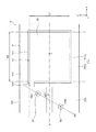
図1は、第1実施形態に係る振動デバイスを示す斜視図である。図2は、図1中のA−A線断面図である。図3は、図1中のB−B線断面図である。図4は、振動素子の上面図である。図5は、振動素子の下面を上側から見た透過図である。図6は、ATカットのカット角を示す図である。図7は、振動素子の下面を上側から見た透過図である。図8は、応力の方向と周波数変動との関係を示すグラフである。図9は、振動素子の変形例を示し、その下面を上側から見た透過図である。
<First Embodiment>
FIG. 1 is a perspective view showing a vibrating device according to the first embodiment. FIG. 2 is a sectional view taken along the line AA in FIG. FIG. 3 is a sectional view taken along the line BB in FIG. FIG. 4 is a top view of the vibrating element. FIG. 5 is a transparent view of the lower surface of the vibrating element as viewed from above. FIG. 6 is a diagram showing the cut angle of the AT cut. FIG. 7 is a transparent view of the lower surface of the vibrating element as viewed from above. FIG. 8 is a graph showing the relationship between the stress direction and frequency fluctuation. FIG. 9 shows a modification of the vibrating element, and is a transparent view of the lower surface of the vibrating element as viewed from above.
図1に示すように、振動デバイス1は、振動素子5と、振動素子5を収納するパッケージ2と、を有する。また、図2および図3に示すように、パッケージ2は、振動素子5を収納する凹部32を有する箱状のリッド3と、凹部32の開口を塞いでリッド3と接合された板状のベース4と、を有する。そして、凹部32の開口がベース4で塞がれることにより、振動素子5を収納する収納空間Sが形成される。収納空間Sは、気密であり、減圧状態、好ましくはより真空に近い状態となっている。ただし、収納空間Sの雰囲気は、特に限定されず、例えば、窒素またはAr等の不活性ガスを封入した雰囲気であってもよく、減圧状態でなく大気圧状態または加圧状態となっていてもよい。
As shown in FIG. 1, the vibrating
ベース4は、絶縁性を有する基板40と、基板40に配置された電極43と、を有する。さらに、基板40は、ベース基板41と、ベース基板41の表面に配置された絶縁膜42と、を有する。
The
ベース基板41は、平面視形状が矩形の板状であり、互いに表裏関係にある下面411および上面412を有する。また、ベース基板41は、その上面412と下面411とを貫通する2つの貫通孔415、416を有する。
The
ベース基板41は、半導体基板である。半導体基板としては、特に限定されず、例えば、シリコン基板、ゲルマニウム基板や、GaP、GaAs、InP等の化合物半導体基板を用いることができる。ベース基板41として半導体基板を用いることにより、振動デバイス1を半導体プロセスによって形成することができるため、振動デバイス1を精度よく製造することができると共に、その小型化を図ることができる。また、ベース4に、例えば、発振回路等の半導体回路を形成することができ、ベース4を有効活用することができる。特に、本実施形態では、ベース基板41として、シリコン基板を用いている。これにより、入手し易く、安価なベース基板41となる。
The
ただし、ベース基板41としては、半導体基板に限定されず、例えば、セラミック基板、ガラス基板等を用いることもできる。なお、セラミック基板やガラス基板を用いた場合のように、ベース基板41自体が絶縁性を有する場合には、絶縁膜42を省略することができる。
However, the
また、ベース基板41の表面には絶縁膜42が配置されている。ただし、絶縁膜42は、上面412の外縁部すなわちリッド3との接合部には配置されていない。そのため、上面412の外縁部は、絶縁膜42から露出している。絶縁膜42は、シリコン酸化膜(SiO2膜)から構成されている。また、絶縁膜42の形成方法としては、特に限定されず、例えば、ベース基板41の表面を熱酸化することにより形成してもよいし、TEOS(テトラエトキシシラン)を用いたプラズマCVDにより形成してもよい。ただし、絶縁膜42としては、特に限定されず、例えば、ポリイミド等の絶縁性の樹脂材料から構成されていてもよいし、異種材料が積層した複合体で構成されていてもよい。
An insulating
また、絶縁膜42上には電極43が配置されている。電極43は、互いに離間して配置された第1配線44および第2配線45を有する。第1配線44は、基板40の上面に配置され、収納空間S内に臨む内部端子441と、基板40の下面に配置され、パッケージ2の外部に臨む外部端子442と、貫通孔415内に配置され、内部端子441と外部端子442とを電気的に接続する貫通電極443と、を有する。
An
同様に、第2配線45は、基板40の上面に配置され、収納空間S内に臨む内部端子451と、基板40の下面に配置され、パッケージ2の外部に臨む外部端子452と、貫通孔416内に配置され、内部端子451と外部端子452とを電気的に接続する貫通電極453と、を有する。
Similarly, the
また、電極43は、基板40の下面に配置された2つのダミー端子461、462を有する。ダミー端子461、462は、電気的な役割を担っておらず、例えば、パッケージ2と対象物との接合強度を高めるために設けられている。ただし、ダミー端子461、462の役割としては、これに限定されない。
In addition, the
リッド3は、その下面31に開口する有底の凹部32を有する箱状をなす。このようなリッド3は、半導体基板である。半導体基板としては、特に限定されず、例えば、シリコン基板、ゲルマニウム基板や、GaP、GaAs、InP等の化合物半導体基板を用いることができる。リッド3として半導体基板を用いることにより、振動デバイス1を半導体プロセスによって形成することができるため、振動デバイス1を精度よく製造することができると共に、その小型化を図ることができる。特に、本実施形態では、リッド3としてシリコン基板を用いている。これにより、入手し易く、安価なリッド3となる。また、ベース基板41とリッド3の材料を揃えることができ、これらの熱膨張係数差を実質的にゼロとすることができる。そのため、熱膨張に起因する熱応力の発生が抑えられ、優れた振動特性を有する振動デバイス1となる。
The
ただし、リッド3としては、半導体基板に限定されず、例えば、セラミック基板、ガラス基板等を用いることもできる。また、リッド3として、ベース基板41と異種の基板を用いてもよい。特に、リッド3として光透過性を有するガラス基板を用いると、振動デバイス1の製造後に、リッド3を介して振動素子5にレーザーを照射して第1励振電極521の一部を除去し、振動素子5の周波数調整を行うことができる。
However, the
このようなリッド3は、その下面31において接合部材6を介してベース基板41の上面412と直接接合されている。本実施形態では、直接接合の中でも金属同士の拡散を利用した拡散接合を用いてリッド3とベース基板41とが接合されている。具体的には、リッド3の下面31に金属膜を設けると共に、ベース基板41の上面412に金属膜を設け、これら金属膜同士を拡散接合することにより接合部材6が形成され、この接合部材6を介してリッド3とベース基板41とが接合されている。ただし、接合方法としては、これに限定されず、例えば、リッド3の下面31とベース基板41の上面412とにアルゴンガス等の不活性ガスを照射して、これらの面を活性し、下面31と上面412とを直接接合してもよい。また、樹脂接着剤、低融点ガラス等の各種接合部材を用いて接合してもよい。
The
図4および図5に示すように、振動素子5は、ATカットの水晶基板51と、水晶基板51の表面に配置された電極52と、を有する。水晶基板51は、厚みすべり振動モードを有し、三次の周波数温度特性を有している。そのため、優れた温度特性を有する振動素子5が得られる。
As shown in FIGS. 4 and 5, the
ATカットの水晶基板51について簡単に説明すると、水晶基板51は、互いに直交する結晶軸X、Y、Zを有している。X軸、Y軸、Z軸は、それぞれ、電気軸、機械軸、光学軸と呼ばれる。図6に示すように、水晶基板51は、X−Z面をX軸回りに所定の角度θ回転させた平面に沿って切り出された「回転Yカット水晶基板」であり、θ=35°15’回転させた平面に沿って切り出した基板を「ATカット水晶基板」という。なお、以下では、角度θに対応してX軸まわりに回転したY軸およびZ軸をY’軸およびZ’軸とする。すなわち、水晶基板51は、Y’軸方向に厚みを有し、X−Z’面方向に広がりを有する。ただし、水晶基板51としては、厚みすべり振動を励振することができ、X軸を含む面方向に広がりを有するものであれば、ATカットの水晶基板に限定されない。なお、以下では、各軸の矢印先端側を「プラス側」とも言い、その反対側を「マイナス側」とも言う。
The AT-
図4および図5に示すように、水晶基板51の外形は、Y’軸方向からの平面視で矩形であり、互いに表裏関係にある下面51aおよび上面51bを有する。そして、水晶基板51は、下面51aをベース4側に向けて配置されている。また、本実施形態では、水晶基板51は、X軸方向を長辺とし、Z’軸方向を短辺とする長手形である。また、水晶基板51は、厚みすべり振動する振動部511と、振動部511の周囲に位置し、振動部511と一体化された支持部512と、を有する。また、水晶基板51は、メサ型をなし、振動部511が支持部512よりも厚く形成されている。振動部511は、支持部512に対してY’軸方向の両側に突出している。
As shown in FIGS. 4 and 5, the outer shape of the
ただし、水晶基板51は、これに限定されず、振動部511と支持部512とが同じ厚さであるフラット型であってもよいし、振動部511が支持部512よりも薄い逆メサ型であってもよい。また、水晶基板51の周囲を研削して面取りするベベル加工や、上面および下面を凸曲面とするコンベックス加工が施されていてもよい。また、メサ型の場合には、下面51a側および上面51b側の一方にだけ突出した構成であってもよいし、逆メサ型の場合には、下面51a側および上面51b側の一方にだけ凹没した構成であってもよい。
However, the
電極52は、振動部511の下面511aに配置された第1励振電極521と、振動部511の上面511bに配置され、振動部511を間に挟んで第1励振電極521と対向する第2励振電極522と、を有する。また、電極52は、支持部512の下面512aに配置された第1パッド電極523および第2パッド電極524と、第1励振電極521と第1パッド電極523とを接続する第1引き出し配線525と、第2励振電極522と第2パッド電極524とを接続する第2引き出し配線526と、を有する。
The
このような振動素子5は、図2および図3に示すように、導電性の第1接合部材B1および第2接合部材B2によってベース4の上面に固定されている。また、第1接合部材B1は、ベース4が有する内部端子441と振動素子5が有する第1パッド電極523とを電気的に接続し、第2接合部材B2は、ベース4が有する内部端子451と振動素子5が有する第2パッド電極524とを電気的に接続している。
As shown in FIGS. 2 and 3, the vibrating
第1、第2接合部材B1、B2としては、導電性と接合性とを兼ね備えていれば、特に限定されず、例えば、金バンプ、銀バンプ、銅バンプ、はんだバンプ等の各種金属バンプ、ポリイミド系、エポキシ系、シリコーン系、アクリル系の各種接着剤に銀フィラー等の導電性フィラーを分散させた導電性接着剤等を用いることができる。第1、第2接合部材B1、B2として前者の金属バンプを用いると、第1、第2接合部材B1、B2からのガスの発生を抑制でき、収納空間Sの環境変化、特に圧力の上昇を効果的に抑制することができる。一方、第1、第2接合部材B1、B2として後者の導電性接着剤を用いると、第1、第2接合部材B1、B2が金属パンプに比べて柔らかくなり、振動素子5に応力が生じ難くなる。
The first and second bonding members B1 and B2 are not particularly limited as long as they have both conductivity and bondability, and examples thereof include various metal bumps such as gold bumps, silver bumps, copper bumps, and solder bumps, and polyimide. It is possible to use a conductive adhesive in which a conductive filler such as a silver filler is dispersed in various adhesives of epoxy, epoxy, silicone, and acrylic. If the former metal bumps are used as the first and second joining members B1 and B2, the generation of gas from the first and second joining members B1 and B2 can be suppressed, and the environmental change of the storage space S, especially the increase in pressure can be prevented. It can be effectively suppressed. On the other hand, when the latter conductive adhesive is used as the first and second joining members B1 and B2, the first and second joining members B1 and B2 become softer than metal pumps, and stress is less likely to occur in the
以上、振動デバイス1の全体構成について説明した。次に、図7に基づいて、振動デバイス1の特徴の1つでもある第1、第2接合部材B1、B2の配置について説明する。なお、以下では、振動素子5の厚さ方向すなわちY’軸方向からの平面視(以下、単に「平面視」とも言う)で、第1励振電極521をX軸方向に延長した領域を第1領域Q1とし、第1励振電極521をZ’軸方向に延長した領域を第2領域Q2とする。第1接合部材B1および第2接合部材B2は、それぞれ、第2領域Q2の外側に位置し、かつ、第2領域Q2に対して同じ側、本実施形態では、X軸方向マイナス側に位置している。このように、第1、第2接合部材B1、B2を第2領域Q2に対して同じ側に配置することにより、振動素子5の小型化を図ることができる。
The overall configuration of the vibrating
また、第1接合部材B1および第2接合部材B2は、それぞれ、第1領域Q1の内側に位置している。このように、第1、第2接合部材B1、B2を第1領域Q1の内側に配置することにより、振動素子5の小型化を図ることができる。
The first joining member B1 and the second joining member B2 are located inside the first region Q1. By arranging the first and second joining members B1 and B2 inside the first region Q1 in this way, the
また、平面視で、振動素子5の重心Gを通り、かつ、X軸と平行な仮想線を第1仮想線α1としたとき、第1接合部材B1は、第1仮想線α1に対して一方側、本実施形態ではZ’軸方向プラス側に位置している。一方、第2接合部材B2は、第1仮想線α1に対して他方側、本実施形態ではZ’軸方向マイナス側に位置している。また、平面視で、第1接合部材B1と第2接合部材B2とを通る仮想線を第2仮想線α2としたとき、第2仮想線α2は、第1仮想線α1すなわちX軸に対して傾斜している。第1、第2接合部材B1、B2をこのように配置することにより、第1、第2接合部材B1、B2を振動素子5の長手方向および短手方向にそれぞれ離間して配置することができるため、振動素子5をバランスよく、安定した姿勢で支持することができる。
Further, when a virtual line passing through the center of gravity G of the vibrating
第1仮想線α1と第2仮想線α2とのなす角θ1は、100°<θ1<140°の関係を満足している。これにより、振動素子5の応力感度(周波数変化/応力)が十分に小さくなる。つまり、応力による周波数変動が十分に小さくなる。そのため、例えば、ベース基板41と水晶基板51との熱膨張係数の差に起因して生じる熱応力が振動素子5に加わっても、さらには、その大小によっても、振動素子5の周波数特性をほぼ一定に保つことができる。したがって、安定した振動特性を有する振動デバイス1となる。
The angle θ1 formed by the first virtual line α1 and the second virtual line α2 satisfies the relationship of 100°<θ1<140°. As a result, the stress sensitivity (frequency change/stress) of the
以下、この理由について簡単に説明する。図8は、応力Fの方向と、受けた応力に起因した周波数変動の関係を示すグラフである。同図から、応力の方向がX軸から120°程度傾斜している場合(=t1)に、周波数変動がゼロであることが分かる。そのため、前述したように、100°<θ1<140°の関係を満足することにより、振動素子5の応力感度が十分に小さくなり、応力に起因する周波数変動を十分に小さく抑えることができる。なお、100°<θ1<140°であれば、特に限定されないが、105°<θ1<135°であることが好ましく、110°<θ1<130°であることがより好ましい。これにより、上述の効果をより顕著に発揮することができる。
The reason for this will be briefly described below. FIG. 8 is a graph showing the relationship between the direction of the stress F and the frequency variation caused by the received stress. From the figure, it can be seen that the frequency fluctuation is zero when the stress direction is inclined by about 120° from the X axis (=t1). Therefore, as described above, by satisfying the relationship of 100°<θ1<140°, the stress sensitivity of the vibrating
特に、本実施形態では、第1、第2接合部材B1、B2を介して振動素子5が取り付けられているベース基板41がシリコン基板で構成されている。シリコンの線膨張係数が2.8ppm/℃であるのに対して、水晶のX軸方向の線膨張係数が13.7ppm/℃であり、Z’軸方向の線膨張係数が11.6ppm/℃である。このように、シリコンと水晶とでは線膨張係数が大きく異なっているため、本実施形態の振動デバイス1は、振動素子5に熱応力が加わり易く、その強さも大きくなり易い構成となっている。そのため、40°<θ1<80°を満足することにより、その効果がより大きなものとなる。なお、例えば、ベース基板41に適用可能なセラミック基板の線膨張係数は、7.0ppm/℃であり、シリコンと比べて水晶との線膨張係数の差が小さい。そのため、振動素子5に熱応力が加わり難く、その強さも大きくなり難い。このようなことからも、ベース基板41がシリコン基板である場合に、特に、その効果を発揮することができると言える。
In particular, in this embodiment, the
なお、図8に示すように、応力Fの方向がX軸から120°傾斜している場合(=t2)にも、周波数変動がゼロであることが分かる。そのため、本実施形態の変形例として、図9に示すように、40°<θ1<80°となるように、第1、第2接合部材B1、B2が配置されていてもよい。このような配置によっても、振動素子5の応力感度が十分に小さくなり、応力に起因する周波数変動を十分に小さく抑えることができる。なお、40°<θ1<80°であれば、特に限定されないが、45°<θ1<75°であることが好ましく、50°<θ1<70°であることがより好ましい。これにより、上述の効果をより顕著に発揮することができる。
Note that, as shown in FIG. 8, even when the direction of the stress F is inclined by 120° from the X axis (=t2), it can be seen that the frequency fluctuation is zero. Therefore, as a modification of the present embodiment, as shown in FIG. 9, the first and second joining members B1 and B2 may be arranged so that 40°<θ1<80°. Even with such an arrangement, the stress sensitivity of the vibrating
ここで、第2仮想線α2は、平面視で、第1接合部材B1および第2接合部材B2と重なっているか接していればよいが、好ましくは、第1接合部材B1の中心Ob1と第2接合部材B2の中心Ob2とを通る仮想線であることが好ましい。これにより、上述した効果をより確実に発揮することができる。 Here, the second virtual line α2 may overlap or contact the first joining member B1 and the second joining member B2 in a plan view, but preferably the center Ob1 of the first joining member B1 and the second An imaginary line passing through the center Ob2 of the joining member B2 is preferable. Thereby, the above-mentioned effect can be exhibited more reliably.
以上、振動デバイス1について説明した。このような振動デバイス1は、前述したように、互いに表裏関係にあり、電気軸であるX軸に沿っている第1面である下面51aおよび第2面である上面51bを含む水晶基板51と、下面51aに配置されている第1励振電極521と、上面51bに、第1励振電極521と対向して配置されている第2励振電極522と、下面51aに配置され、第1励振電極521と電気的に接続されている第1パッド電極523と、下面51aに配置され、第2励振電極522と電気的に接続されている第2パッド電極524と、を含む振動素子5と、基板40と、基板40に配置されている第1配線44および第2配線45と、を含むベース4と、第1パッド電極523と第1配線44とを接合する第1接合部材B1と、第2パッド電極524と第2配線45とを接合する第2接合部材B2と、を備える。また、水晶基板51の平面視で、振動素子5の重心Gを通り、かつ、X軸と平行な直線を第1仮想線α1としたとき、第1接合部材B1は、平面視で、第1仮想線α1に対して一方側に位置し、第2接合部材B2は、平面視で、第1仮想線α1に対して他方側に位置する。そして、平面視で、第1接合部材B1と第2接合部材B2とを通る直線を第2仮想線α2とし、第1仮想線α1と第2仮想線α2とのなす角をθ1としたとき、40°<θ1<80°または100°<θ1<140°を満足する。
The vibrating
このような構成とすることにより、振動素子5の応力感度が十分に小さくなる。そのため、振動素子5に応力が加わっても、さらには、その大きさによっても、振動素子5の周波数特性をほぼ一定に保つことができる。したがって、安定した振動特性を有する振動デバイス1となる。また、第1、第2接合部材B1、B2をX軸方向およびZ’軸方向にそれぞれ離間して配置することができ、第1、第2接合部材B1、B2が振動素子5のZ’軸方向の一方側に偏って配置されることもないため、振動素子5をバランスよく、安定した姿勢で支持することができる。したがって、衝撃等によっても、振動素子5が変形し難く、より安定した振動特性を発揮することができる。
With such a configuration, the stress sensitivity of the
また、前述したように、振動デバイス1は、45°<θ1<75°または105°<θ1<135°を満足することが好ましい。これにより、上述した効果をより顕著に発揮することができ、より安定した振動特性を有する振動デバイス1となる。
Further, as described above, the vibrating
また、前述したように、平面視で、第1励振電極521を前記X軸方向に延長した領域を第1領域Q1としたとき、第1接合部材B1および第2接合部材B2は、それぞれ、第1領域Q1の内側に位置している。これにより、振動デバイス1の小型化を図ることができる。
Further, as described above, when the region where the
また、前述したように、平面視で、第1励振電極521をX軸に直交する方向すなわちZ’軸方向に延長した領域を第2領域Q2としたとき、第1接合部材B1および第2接合部材B2は、それぞれ、第2領域Q2の外側に位置し、かつ、第2領域Q2に対して同じ側、本実施形態ではX軸方向マイナス側に位置している。これにより、振動デバイス1の小型化を図ることができる。
Further, as described above, when the region extending the
また、前述したように、基板40は、シリコン基板を含んでいる。シリコンと水晶とでは線膨張係数が大きく異なっているため、振動デバイス1は、振動素子5に熱応力が加わり易く、その強さも大きくなり易い構成となる。したがって、上述した効果がより寄与する構成となる。
Further, as described above, the
<第2実施形態>
図10は、第2実施形態に係る振動素子の下面を上側から見た透過図である。図11は、振動素子の変形例を示し、その下面を上側から見た透過図である。
<Second Embodiment>
FIG. 10 is a transparent view of the lower surface of the resonator element according to the second embodiment as viewed from above. FIG. 11 shows a modification of the vibrating element, and is a transparent view of the lower surface of the vibrating element as seen from above.
本実施形態に係る振動デバイス1は、第1、第2接合部材B1、B2の配置が異なること以外は、前述した第1実施形態の振動デバイス1と同様である。なお、以下の説明では、第2実施形態の振動デバイス1に関し、前述した第1実施形態との相違点を中心に説明し、同様の事項に関してはその説明を省略する。また、図10および図11では、前述した実施形態と同様の構成について、同一符号を付している。
The vibrating
図10に示すように、第1接合部材B1は、第1仮想線α1に対して一方側、本実施形態ではZ’軸方向プラス側に位置している。一方、第2接合部材B2は、平面視で、第1仮想線α1と重なっている。また、第1仮想線α1と第2仮想線α2とのなす角θ1は、100°<θ1<140°の関係を満足している。このような配置によっても、振動素子5の応力感度が十分に小さくなり、応力に起因する周波数変動を十分に小さく抑えることができる。なお、本実施形態の変形例として、図11に示すように、40°<θ1<80°となるように、第1、第2接合部材B1、B2が配置されていてもよく、本実施形態と同様の効果を発揮することができる。
As shown in FIG. 10, the first joining member B1 is located on one side with respect to the first imaginary line α1, that is, on the Z′ axis direction plus side in the present embodiment. On the other hand, the second joining member B2 overlaps the first imaginary line α1 in a plan view. The angle θ1 formed by the first virtual line α1 and the second virtual line α2 satisfies the relationship of 100°<θ1<140°. Even with such an arrangement, the stress sensitivity of the vibrating
以上のように、本実施形態の振動デバイス1では、水晶基板51の平面視で、振動素子5の重心Gを通り、かつ、X軸と平行な直線を第1仮想線α1としたとき、第1接合部材B1は、平面視で、第1仮想線α1に対して一方側に位置し、第2接合部材B2は、平面視で、第1仮想線α1と重なっている。そして、平面視で、第1接合部材B1と第2接合部材B2とを通る直線を第2仮想線α2とし、第1仮想線α1と第2仮想線α2とのなす角をθ1としたとき、40°<θ1<80°または100°<θ1<140°である。
As described above, in the vibrating
このような構成とすることにより、振動素子5の応力感度が十分に小さくなる。そのため、振動素子5に応力が加わっても、さらには、その大きさによっても、振動素子5の周波数特性をほぼ一定に保つことができる。したがって、安定した振動特性を有する振動デバイス1となる。また、第1、第2接合部材B1、B2をX軸方向およびZ’軸方向にそれぞれ離間して配置することができ、第1、第2接合部材B1、B2が振動素子5のZ’軸方向の一方側に偏って配置されることもないため、振動素子5をバランスよく、安定した姿勢で支持することができる。したがって、衝撃等によっても、振動素子5が変形し難く、より安定した振動特性を発揮することができる。
With such a configuration, the stress sensitivity of the
このような第2実施形態によっても、前述した第1実施形態と同様の効果を発揮することができる。 According to such a second embodiment, the same effect as that of the above-described first embodiment can be exhibited.
<第3実施形態>
図12は、第3実施形態に係る振動素子の下面を上側から見た透過図である。
<Third Embodiment>
FIG. 12 is a transparent view of the lower surface of the resonator element according to the third embodiment as viewed from above.
本実施形態に係る振動デバイス1は、第1、第2接合部材B1、B2の配置が異なること以外は、前述した第1実施形態の振動デバイス1と同様である。なお、以下の説明では、第3実施形態の振動デバイス1に関し、前述した第1実施形態との相違点を中心に説明し、同様の事項に関してはその説明を省略する。また、図12では、前述した実施形態と同様の構成について、同一符号を付している。
The vibrating
図12に示すように、第1接合部材B1は、第1領域Q1の外側、本実施形態では第1領域Q1に対してZ’軸方向プラス側に位置している。一方、第2接合部材B2は、第1領域Q1の外側、本実施形態では第1領域Q1に対してZ’軸方向マイナス側に位置している。つまり、第1、第2接合部材B1、B2は、第1領域Q1を間に挟んで配置されている。このような構成とすることにより、第1、第2接合部材B1、B2を十分に離間して配置することができ、振動素子5をより安定した姿勢でベース4に取り付けることができる。
As shown in FIG. 12, the first joining member B1 is located outside the first region Q1, that is, in the present embodiment, on the Z′ axis direction plus side with respect to the first region Q1. On the other hand, the second joining member B2 is located outside the first region Q1, that is, in the present embodiment, on the minus side in the Z′-axis direction with respect to the first region Q1. That is, the first and second joining members B1 and B2 are arranged with the first region Q1 interposed therebetween. With such a configuration, the first and second joining members B1 and B2 can be arranged sufficiently separated, and the vibrating
以上のように、本実施形態の振動デバイス1では、平面視で、第1励振電極521をX軸方向に延長した領域を第1領域Q1としたとき、第1接合部材B1および第2接合部材B2は、それぞれ、第1領域Q1の外側に位置し、かつ、第1領域Q1を間に挟んで配置されている。このような構成とすることにより、第1、第2接合部材B1、B2を十分に離間して配置することができ、振動素子5をより安定した姿勢でベース4に取り付けることができる。
As described above, in the vibrating
このような第3実施形態によっても、前述した第1実施形態と同様の効果を発揮することができる。なお、本実施形態の変形例として、例えば、第1、第2接合部材B1、B2のいずれか一方が第1領域Q1内に位置していてもよい。 According to such a third embodiment, the same effect as that of the above-described first embodiment can be exhibited. As a modified example of the present embodiment, for example, one of the first and second joining members B1 and B2 may be located in the first region Q1.
<第4実施形態>
図13は、第4実施形態に係る振動モジュールを示す断面図である。
<Fourth Embodiment>
FIG. 13 is a sectional view showing a vibration module according to the fourth embodiment.
図13に示す振動モジュール1000は、支持基板1010と、支持基板1010に搭載された回路基板1020と、回路基板1020に搭載された振動デバイス1と、回路基板1020および振動デバイス1をモールドするモールド材Mと、を有する。
A vibrating
支持基板1010は、例えば、インターポーザー基板である。支持基板1010の上面には複数の接続端子1011が配置され、下面には複数の実装端子1012が配置されている。また、支持基板1010内には図示しない内部配線が配置され、この内部配線を介して、各接続端子1011が、対応する実装端子1012と電気的に接続されている。このような支持基板1010としては、特に限定されず、例えば、シリコン基板、セラミック基板、樹脂基板、ガラス基板、ガラスエポキシ基板等を用いることができる。
The
また、回路基板1020は、ダイアタッチ材を介して支持基板1010の上面に接合されている。回路基板1020は、振動デバイス1が有する振動素子5を発振させてクロック信号等の基準信号の周波数を生成する発振回路1023が形成されており、その上面に発振回路と電気的に接続された複数の端子1022が配置されている。そして、一部の端子1022は、ボンディングワイヤーBWを介して接続端子1011と電気的に接続されており、一部の端子1022は、例えば、半田等の導電性接合部材B3を介して振動デバイス1と電気的に接続されている。
The
モールド材Mは、回路基板1020および振動デバイス1をモールドし、水分、埃、衝撃等から保護している。モールド材Mとしては、特に限定されないが、例えば、熱硬化型のエポキシ樹脂を用いることができ、トランスファーモールド法によってモールドすることができる。
The molding material M molds the
以上のような振動モジュール1000は、振動デバイス1を備える。そのため、前述した振動デバイス1の効果を享受でき、優れた信頼性を発揮することができる。
The vibrating
<第5実施形態>
図14は、第5実施形態に係る電子機器を示す斜視図である。
<Fifth Embodiment>
FIG. 14 is a perspective view showing an electronic device according to the fifth embodiment.
図14に示すラップトップ型のパーソナルコンピューター1100は、本発明の振動デバイスを備える電子機器を適用したものである。この図において、パーソナルコンピューター1100は、キーボード1102を備えた本体部1104と、表示部1108を備えた表示ユニット1106とにより構成され、表示ユニット1106は、本体部1104に対しヒンジ構造部を介して回動可能に支持されている。このようなパーソナルコンピューター1100には、例えば、発振器として用いられる振動デバイス1が内蔵されている。
A laptop
このように、電子機器としてのパーソナルコンピューター1100は、振動デバイス1を備える。そのため、前述した振動デバイス1の効果を享受でき、高い信頼性を発揮することができる。
As described above, the
<第6実施形態>
図15は、第6実施形態に係る電子機器を示す斜視図である。
<Sixth Embodiment>
FIG. 15 is a perspective view showing an electronic device according to the sixth embodiment.
図15に示す携帯電話機1200は、本発明の振動デバイスを備える電子機器を適用したものである。携帯電話機1200は、図示しないアンテナ、複数の操作ボタン1202、受話口1204および送話口1206を備え、操作ボタン1202と受話口1204との間には表示部1208が配置されている。このような携帯電話機1200には、例えば、発振器として用いられる振動デバイス1が内蔵されている。
A
このように、電子機器としての携帯電話機1200は、振動デバイス1を備える。そのため、前述した振動デバイス1の効果を享受でき、高い信頼性を発揮することができる。
As described above, the
<第7実施形態>
図16は、本発明の第7実施形態に係る電子機器を示す斜視図である。
<Seventh Embodiment>
FIG. 16 is a perspective view showing an electronic device according to the seventh embodiment of the present invention.
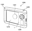
図16に示すデジタルスチールカメラ1300は、本発明の振動デバイスを備える電子機器を適用したものである。ボディ1302の背面には表示部1310が設けられ、CCDによる撮像信号に基づいて表示を行う構成になっており、表示部1310は、被写体を電子画像として表示するファインダーとして機能する。また、ボディ1302の正面側(図中裏面側)には、光学レンズやCCDなどを含む受光ユニット1304が設けられている。そして、撮影者が表示部1310に表示された被写体像を確認し、シャッターボタン1306を押すと、その時点におけるCCDの撮像信号が、メモリー1308に転送・格納される。このようなデジタルスチールカメラ1300には、例えば、発振器として用いられる振動デバイス1が内蔵されている。
A
このように、電子機器としてのデジタルスチールカメラ1300は、振動デバイス1を備える。そのため、前述した振動デバイス1の効果を享受でき、高い信頼性を発揮することができる。
As described above, the
なお、本発明の電子機器は、前述したパーソナルコンピューター、携帯電話機およびデジタルスチールカメラの他にも、例えば、スマートフォン、タブレット端末、時計(スマートウォッチを含む)、インクジェット式吐出装置(例えばインクジェットプリンタ)、デスクトップ型パーソナルコンピューター、テレビ、HMD(ヘッドマウントディスプレイ)等のウェアラブル端末、ビデオカメラ、ビデオテープレコーダー、カーナビゲーション装置、ページャ、電子手帳(通信機能付も含む)、電子辞書、電卓、電子ゲーム機器、ワードプロセッサー、ワークステーション、テレビ電話、防犯用テレビモニター、電子双眼鏡、POS端末、医療機器(例えば電子体温計、血圧計、血糖計、心電図計測装置、超音波診断装置、電子内視鏡)、魚群探知機、各種測定機器、移動体端末基地局用機器、計器類(例えば、車両、航空機、船舶の計器類)、フライトシミュレーター、ネットワークサーバー等に適用することができる。 The electronic device of the present invention includes, for example, a smartphone, a tablet terminal, a watch (including a smart watch), an inkjet discharge device (for example, an inkjet printer), in addition to the personal computer, the mobile phone, and the digital still camera described above. Wearable terminals such as desktop personal computers, televisions, HMDs (head mounted displays), video cameras, video tape recorders, car navigation devices, pagers, electronic organizers (including communication functions), electronic dictionaries, calculators, electronic game devices, Word processors, workstations, videophones, crime prevention TV monitors, electronic binoculars, POS terminals, medical devices (eg electronic thermometers, blood pressure monitors, blood glucose meters, electrocardiogram measurement devices, ultrasonic diagnostic devices, electronic endoscopes), fish finder The present invention can be applied to various measuring devices, mobile terminal base station devices, measuring instruments (for example, measuring instruments for vehicles, aircrafts, ships), flight simulators, network servers, and the like.
<第8実施形態>
図17は、第8実施形態に係る移動体を示す斜視図である。
<Eighth Embodiment>
FIG. 17 is a perspective view showing a moving body according to the eighth embodiment.
図17に示す自動車1500は、本発明の振動デバイスを備える移動体を適用した自動車である。自動車1500には、例えば、発振器として用いられる振動デバイス1が内蔵されている。振動デバイス1は、例えば、キーレスエントリー、イモビライザー、カーナビゲーションシステム、カーエアコン、アンチロックブレーキシステム(ABS)、エアバック、タイヤ・プレッシャー・モニタリング・システム(TPMS:Tire Pressure Monitoring System)、エンジンコントロール、ハイブリッド自動車や電気自動車の電池モニター、車体姿勢制御システム等の電子制御ユニット(ECU:electronic control unit)に広く適用できる。
A
このように、移動体としての自動車1500は、振動デバイス1を備える。そのため、前述した振動デバイス1の効果を享受でき、高い信頼性を発揮することができる。
As described above, the
なお、移動体としては、自動車1500に限定されず、例えば、飛行機、船舶、AGV(無人搬送車)、二足歩行ロボット、ドローン等の無人飛行機等にも適用することができる。
The moving body is not limited to the
以上、本適用例の振動デバイス、振動モジュール、電子機器および移動体を図示の実施形態に基づいて説明したが、本発明はこれに限定されるものではなく、各部の構成は、同様の機能を有する任意の構成のものに置換することができる。また、本発明に、他の任意の構成物が付加されていてもよい。また、本発明は、前記各実施形態のうちの、任意の2以上の構成を組み合わせたものであってもよい。 Although the vibrating device, the vibrating module, the electronic device, and the moving body of the application example have been described above based on the illustrated embodiment, the present invention is not limited to this, and the configuration of each unit has the same function. It can be replaced with one having any configuration. Moreover, other arbitrary components may be added to the present invention. Further, the present invention may be a combination of any two or more configurations of the above embodiments.
1…振動デバイス、2…パッケージ、3…リッド、31…下面、32…凹部、4…ベース、40…基板、41…ベース基板、411…下面、412…上面、415…貫通孔、416…貫通孔、42…絶縁膜、43…電極、44…第1配線、441…内部端子、442…外部端子、443…貫通電極、45…第2配線、451…内部端子、452…外部端子、453…貫通電極、461…ダミー端子、462…ダミー端子、5…振動素子、51…水晶基板、51a…下面、51b…上面、511…振動部、511a…下面、511b…上面、512…支持部、512a…下面、52…電極、521…第1励振電極、522…第2励振電極、523…第1パッド電極、524…第2パッド電極、525…第1引き出し配線、526…第2引き出し配線、6…接合部材、1000…振動モジュール、1010…支持基板、1011…接続端子、1012…実装端子、1020…回路基板、1022…端子、1023…発振回路、1100…パーソナルコンピューター、1102…キーボード、1104…本体部、1106…表示ユニット、1108…表示部、1200…携帯電話機、1202…操作ボタン、1204…受話口、1206…送話口、1208…表示部、1300…デジタルスチールカメラ、1302…ボディ、1304…受光ユニット、1306…シャッターボタン、1308…メモリー、1310…表示部、1500…自動車、B1…第1接合部材、B2…第2接合部材、B3…導電性接合部材、BW…ボンディングワイヤー、G…重心、M…モールド材、Ob1、Ob2…中心、Q1…第1領域、Q2…第2領域、S…収納空間、α1…第1仮想線、α2…第2仮想線、θ…角度、θ1…角
DESCRIPTION OF
Claims (9)
前記第1面に配置されている第1励振電極と、
前記第2面に、前記第1励振電極と対向して配置されている第2励振電極と、
前記第1面に配置され、前記第1励振電極と電気的に接続されている第1パッド電極と、
前記第1面に配置され、前記第2励振電極と電気的に接続されている第2パッド電極と、
を含む振動素子と、
基板と、
前記基板に配置されている第1配線および第2配線と、
を含むベースと、
前記第1パッド電極と前記第1配線とを接合する第1接合部材と、
前記第2パッド電極と前記第2配線とを接合する第2接合部材と、
を備え、
前記水晶基板の平面視で、前記振動素子の重心を通り、かつ、前記X軸と平行な直線を第1仮想線としたとき、
前記第1接合部材は、前記平面視で、前記第1仮想線に対して一方側に位置し、
前記第2接合部材は、前記平面視で、前記第1仮想線と重なるか、または前記第1仮想線に対して他方側に位置し、
前記平面視で、前記第1接合部材と前記第2接合部材とを通る直線を第2仮想線とし、前記第1仮想線と前記第2仮想線とのなす角をθ1としたとき、
40°<θ1<80°または100°<θ1<140°を満足することを特徴とする振動デバイス。 A quartz substrate having a first surface and a second surface which are in a front-back relationship with each other and are along an X axis which is an electric axis;
A first excitation electrode disposed on the first surface,
A second excitation electrode disposed on the second surface so as to face the first excitation electrode;
A first pad electrode disposed on the first surface and electrically connected to the first excitation electrode;
A second pad electrode disposed on the first surface and electrically connected to the second excitation electrode;
A vibrating element including
Board,
A first wiring and a second wiring arranged on the substrate;
Including the base,
A first joining member for joining the first pad electrode and the first wiring;
A second joining member for joining the second pad electrode and the second wiring;
Equipped with
When a straight line that passes through the center of gravity of the vibrating element and that is parallel to the X axis is a first virtual line in a plan view of the quartz substrate,
The first joining member is located on one side with respect to the first virtual line in the plan view,
The second joining member overlaps with the first virtual line or is located on the other side with respect to the first virtual line in the plan view,
In the plan view, when a straight line passing through the first joining member and the second joining member is a second virtual line and an angle formed by the first virtual line and the second virtual line is θ1,
A vibrating device satisfying 40°<θ1<80° or 100°<θ1<140°.
前記第1接合部材および前記第2接合部材は、それぞれ、前記第1領域の内側に位置している請求項1または2に記載の振動デバイス。 In the plan view, when a region in which the first excitation electrode is extended in the X-axis direction is a first region,
The vibrating device according to claim 1, wherein the first joining member and the second joining member are located inside the first region, respectively.
前記第1接合部材および前記第2接合部材は、それぞれ、前記第1領域の外側に位置し、かつ、前記第1領域を間に挟んで配置されている請求項1または2に記載の振動デバイス。 In the plan view, when a region in which the first excitation electrode is extended in the X-axis direction is a first region,
The vibrating device according to claim 1 or 2, wherein the first joining member and the second joining member are respectively located outside the first region and sandwich the first region therebetween. ..
前記第1接合部材および前記第2接合部材は、それぞれ、前記第2領域の外側に位置し、かつ、前記第2領域に対して同じ側に位置している請求項1ないし4のいずれか1項に記載の振動デバイス。 In the plan view, when a region that extends the first excitation electrode in a direction orthogonal to the X axis is a second region,
The first joining member and the second joining member are respectively located outside the second region and on the same side with respect to the second region. The vibrating device according to item.
Priority Applications (3)
| Application Number | Priority Date | Filing Date | Title |
|---|---|---|---|
| JP2019015322A JP2020123881A (en) | 2019-01-31 | 2019-01-31 | Vibration device, vibration module, electronic apparatus, and movable body |
| CN202010076811.5A CN111510103A (en) | 2019-01-31 | 2020-01-23 | Vibration device, vibration module, electronic apparatus, and moving object |
| US16/776,109 US11569795B2 (en) | 2019-01-31 | 2020-01-29 | Resonator device, resonator module, electronic apparatus, and vehicle |
Applications Claiming Priority (1)
| Application Number | Priority Date | Filing Date | Title |
|---|---|---|---|
| JP2019015322A JP2020123881A (en) | 2019-01-31 | 2019-01-31 | Vibration device, vibration module, electronic apparatus, and movable body |
Publications (2)
| Publication Number | Publication Date |
|---|---|
| JP2020123881A true JP2020123881A (en) | 2020-08-13 |
| JP2020123881A5 JP2020123881A5 (en) | 2021-11-25 |
Family
ID=71837950
Family Applications (1)
| Application Number | Title | Priority Date | Filing Date |
|---|---|---|---|
| JP2019015322A Pending JP2020123881A (en) | 2019-01-31 | 2019-01-31 | Vibration device, vibration module, electronic apparatus, and movable body |
Country Status (3)
| Country | Link |
|---|---|
| US (1) | US11569795B2 (en) |
| JP (1) | JP2020123881A (en) |
| CN (1) | CN111510103A (en) |
Families Citing this family (1)
| Publication number | Priority date | Publication date | Assignee | Title |
|---|---|---|---|---|
| JP2022046920A (en) * | 2020-09-11 | 2022-03-24 | セイコーエプソン株式会社 | Electronic device |
Citations (9)
| Publication number | Priority date | Publication date | Assignee | Title |
|---|---|---|---|---|
| JPH1188104A (en) * | 1997-09-10 | 1999-03-30 | Meidensha Corp | At cut crystal vibrator |
| JP2000332571A (en) * | 1999-05-24 | 2000-11-30 | Toyo Commun Equip Co Ltd | Piezoelectric device |
| EP1303042A1 (en) * | 2001-10-09 | 2003-04-16 | Eta SA Fabriques d'Ebauches | Piezoelectrical resonator and unit comprising such a resonator enclosed in a case |
| JP2009016894A (en) * | 2007-06-29 | 2009-01-22 | Citizen Finetech Miyota Co Ltd | Piezoelectric device and manufacturing method thereof |
| JP2011229167A (en) * | 2000-12-12 | 2011-11-10 | Seiko Epson Corp | Surface-mount piezoelectric device |
| JP2013055400A (en) * | 2011-09-01 | 2013-03-21 | Seiko Instruments Inc | Piezoelectric vibration device and generator |
| JP2013157692A (en) * | 2012-01-27 | 2013-08-15 | Seiko Instruments Inc | Vibration device and oscillator |
| JP2016127468A (en) * | 2015-01-06 | 2016-07-11 | セイコーエプソン株式会社 | Vibration device, electronic apparatus and mobile object |
| JP2017055454A (en) * | 2016-12-09 | 2017-03-16 | セイコーエプソン株式会社 | Vibration piece, vibrator, oscillator, electronic apparatus and movable body |
Family Cites Families (6)
| Publication number | Priority date | Publication date | Assignee | Title |
|---|---|---|---|---|
| JP5085682B2 (en) * | 2010-04-26 | 2012-11-28 | 日本電波工業株式会社 | Piezoelectric device |
| JP5708079B2 (en) | 2011-03-16 | 2015-04-30 | 株式会社大真空 | Crystal oscillator |
| WO2013047807A1 (en) * | 2011-09-30 | 2013-04-04 | 株式会社大真空 | Electronic component package, sealing member for electronic component package, and method for manufacturing sealing member for electronic component package |
| JP6052651B1 (en) * | 2015-03-03 | 2016-12-27 | 株式会社村田製作所 | Crystal oscillator |
| WO2017022504A1 (en) * | 2015-07-31 | 2017-02-09 | 株式会社村田製作所 | Electronic component and method for producing same |
| JP7230541B2 (en) * | 2019-01-31 | 2023-03-01 | セイコーエプソン株式会社 | Vibration device and vibration module |
-
2019
- 2019-01-31 JP JP2019015322A patent/JP2020123881A/en active Pending
-
2020
- 2020-01-23 CN CN202010076811.5A patent/CN111510103A/en active Pending
- 2020-01-29 US US16/776,109 patent/US11569795B2/en active Active
Patent Citations (9)
| Publication number | Priority date | Publication date | Assignee | Title |
|---|---|---|---|---|
| JPH1188104A (en) * | 1997-09-10 | 1999-03-30 | Meidensha Corp | At cut crystal vibrator |
| JP2000332571A (en) * | 1999-05-24 | 2000-11-30 | Toyo Commun Equip Co Ltd | Piezoelectric device |
| JP2011229167A (en) * | 2000-12-12 | 2011-11-10 | Seiko Epson Corp | Surface-mount piezoelectric device |
| EP1303042A1 (en) * | 2001-10-09 | 2003-04-16 | Eta SA Fabriques d'Ebauches | Piezoelectrical resonator and unit comprising such a resonator enclosed in a case |
| JP2009016894A (en) * | 2007-06-29 | 2009-01-22 | Citizen Finetech Miyota Co Ltd | Piezoelectric device and manufacturing method thereof |
| JP2013055400A (en) * | 2011-09-01 | 2013-03-21 | Seiko Instruments Inc | Piezoelectric vibration device and generator |
| JP2013157692A (en) * | 2012-01-27 | 2013-08-15 | Seiko Instruments Inc | Vibration device and oscillator |
| JP2016127468A (en) * | 2015-01-06 | 2016-07-11 | セイコーエプソン株式会社 | Vibration device, electronic apparatus and mobile object |
| JP2017055454A (en) * | 2016-12-09 | 2017-03-16 | セイコーエプソン株式会社 | Vibration piece, vibrator, oscillator, electronic apparatus and movable body |
Also Published As
| Publication number | Publication date |
|---|---|
| US20200252050A1 (en) | 2020-08-06 |
| CN111510103A (en) | 2020-08-07 |
| US11569795B2 (en) | 2023-01-31 |
Similar Documents
| Publication | Publication Date | Title |
|---|---|---|
| JP2018152755A (en) | Vibration device, oscillator, electronic device, and mobile object | |
| US11075613B2 (en) | Vibrator device, electronic apparatus, and vehicle | |
| JP2023065527A (en) | Vibration device, vibration module, and electronic apparatus | |
| JP2020123881A (en) | Vibration device, vibration module, electronic apparatus, and movable body | |
| US11097667B2 (en) | Vibration device, vibration module, electronic apparatus, and vehicle | |
| JP7230541B2 (en) | Vibration device and vibration module | |
| US11183986B2 (en) | Resonator element, resonator device, electronic apparatus, and vehicle | |
| JP7247694B2 (en) | Vibration devices, oscillators, vibration modules, electronic devices and moving objects | |
| JP7200705B2 (en) | Vibration device, manufacturing method of vibration device, vibration module, electronic device, and moving body | |
| JP2020108087A (en) | Vibration device, electronic apparatus, and movable body | |
| JP7367311B2 (en) | Vibration elements, vibration devices, oscillators, electronic equipment and moving objects | |
| JP2015050483A (en) | Electronic device, electronic apparatus, and mobile | |
| JP2019176224A (en) | Vibrator, oscillator, electronic apparatus, and movable body | |
| JP2019145978A (en) | Vibration element, vibrator, oscillator, electronic apparatus, and movable body | |
| JP2020123926A (en) | Vibration device, vibration module, electronic device, moving body, and manufacturing method of vibration device | |
| JP2021175056A (en) | Vibration device, vibration module, electronic apparatus, and movable body | |
| JP2019169796A (en) | Vibration device, electronic apparatus, and movable body | |
| JP2020108088A (en) | Vibration device, electronic apparatus, and movable body |
Legal Events
| Date | Code | Title | Description |
|---|---|---|---|
| RD07 | Notification of extinguishment of power of attorney |
Free format text: JAPANESE INTERMEDIATE CODE: A7427 Effective date: 20200810 |
|
| RD04 | Notification of resignation of power of attorney |
Free format text: JAPANESE INTERMEDIATE CODE: A7424 Effective date: 20210917 |
|
| A521 | Request for written amendment filed |
Free format text: JAPANESE INTERMEDIATE CODE: A523 Effective date: 20211011 |
|
| A621 | Written request for application examination |
Free format text: JAPANESE INTERMEDIATE CODE: A621 Effective date: 20211011 |
|
| RD03 | Notification of appointment of power of attorney |
Free format text: JAPANESE INTERMEDIATE CODE: A7423 Effective date: 20211108 |
|
| A977 | Report on retrieval |
Free format text: JAPANESE INTERMEDIATE CODE: A971007 Effective date: 20220817 |
|
| A131 | Notification of reasons for refusal |
Free format text: JAPANESE INTERMEDIATE CODE: A131 Effective date: 20220830 |
|
| A521 | Request for written amendment filed |
Free format text: JAPANESE INTERMEDIATE CODE: A523 Effective date: 20221021 |
|
| A131 | Notification of reasons for refusal |
Free format text: JAPANESE INTERMEDIATE CODE: A131 Effective date: 20230221 |
|
| A521 | Request for written amendment filed |
Free format text: JAPANESE INTERMEDIATE CODE: A523 Effective date: 20230413 |
|
| A02 | Decision of refusal |
Free format text: JAPANESE INTERMEDIATE CODE: A02 Effective date: 20230725 |