JP7149164B2 - 表示装置 - Google Patents
表示装置 Download PDFInfo
- Publication number
- JP7149164B2 JP7149164B2 JP2018207672A JP2018207672A JP7149164B2 JP 7149164 B2 JP7149164 B2 JP 7149164B2 JP 2018207672 A JP2018207672 A JP 2018207672A JP 2018207672 A JP2018207672 A JP 2018207672A JP 7149164 B2 JP7149164 B2 JP 7149164B2
- Authority
- JP
- Japan
- Prior art keywords
- light emitting
- emitting element
- gradation value
- green light
- pixel
- Prior art date
- Legal status (The legal status is an assumption and is not a legal conclusion. Google has not performed a legal analysis and makes no representation as to the accuracy of the status listed.)
- Active
Links
Images


Classifications
-
- H—ELECTRICITY
- H01—ELECTRIC ELEMENTS
- H01L—SEMICONDUCTOR DEVICES NOT COVERED BY CLASS H10
- H01L25/00—Assemblies consisting of a plurality of individual semiconductor or other solid state devices ; Multistep manufacturing processes thereof
- H01L25/16—Assemblies consisting of a plurality of individual semiconductor or other solid state devices ; Multistep manufacturing processes thereof the devices being of types provided for in two or more different main groups of groups H01L27/00 - H01L33/00, or in a single subclass of H10K, H10N, e.g. forming hybrid circuits
- H01L25/167—Assemblies consisting of a plurality of individual semiconductor or other solid state devices ; Multistep manufacturing processes thereof the devices being of types provided for in two or more different main groups of groups H01L27/00 - H01L33/00, or in a single subclass of H10K, H10N, e.g. forming hybrid circuits comprising optoelectronic devices, e.g. LED, photodiodes
-
- G—PHYSICS
- G09—EDUCATION; CRYPTOGRAPHY; DISPLAY; ADVERTISING; SEALS
- G09F—DISPLAYING; ADVERTISING; SIGNS; LABELS OR NAME-PLATES; SEALS
- G09F9/00—Indicating arrangements for variable information in which the information is built-up on a support by selection or combination of individual elements
- G09F9/30—Indicating arrangements for variable information in which the information is built-up on a support by selection or combination of individual elements in which the desired character or characters are formed by combining individual elements
- G09F9/302—Indicating arrangements for variable information in which the information is built-up on a support by selection or combination of individual elements in which the desired character or characters are formed by combining individual elements characterised by the form or geometrical disposition of the individual elements
-
- G—PHYSICS
- G09—EDUCATION; CRYPTOGRAPHY; DISPLAY; ADVERTISING; SEALS
- G09F—DISPLAYING; ADVERTISING; SIGNS; LABELS OR NAME-PLATES; SEALS
- G09F9/00—Indicating arrangements for variable information in which the information is built-up on a support by selection or combination of individual elements
- G09F9/30—Indicating arrangements for variable information in which the information is built-up on a support by selection or combination of individual elements in which the desired character or characters are formed by combining individual elements
- G09F9/33—Indicating arrangements for variable information in which the information is built-up on a support by selection or combination of individual elements in which the desired character or characters are formed by combining individual elements being semiconductor devices, e.g. diodes
-
- G—PHYSICS
- G09—EDUCATION; CRYPTOGRAPHY; DISPLAY; ADVERTISING; SEALS
- G09G—ARRANGEMENTS OR CIRCUITS FOR CONTROL OF INDICATING DEVICES USING STATIC MEANS TO PRESENT VARIABLE INFORMATION
- G09G3/00—Control arrangements or circuits, of interest only in connection with visual indicators other than cathode-ray tubes
- G09G3/20—Control arrangements or circuits, of interest only in connection with visual indicators other than cathode-ray tubes for presentation of an assembly of a number of characters, e.g. a page, by composing the assembly by combination of individual elements arranged in a matrix no fixed position being assigned to or needed to be assigned to the individual characters or partial characters
- G09G3/2003—Display of colours
-
- G—PHYSICS
- G09—EDUCATION; CRYPTOGRAPHY; DISPLAY; ADVERTISING; SEALS
- G09G—ARRANGEMENTS OR CIRCUITS FOR CONTROL OF INDICATING DEVICES USING STATIC MEANS TO PRESENT VARIABLE INFORMATION
- G09G3/00—Control arrangements or circuits, of interest only in connection with visual indicators other than cathode-ray tubes
- G09G3/20—Control arrangements or circuits, of interest only in connection with visual indicators other than cathode-ray tubes for presentation of an assembly of a number of characters, e.g. a page, by composing the assembly by combination of individual elements arranged in a matrix no fixed position being assigned to or needed to be assigned to the individual characters or partial characters
- G09G3/22—Control arrangements or circuits, of interest only in connection with visual indicators other than cathode-ray tubes for presentation of an assembly of a number of characters, e.g. a page, by composing the assembly by combination of individual elements arranged in a matrix no fixed position being assigned to or needed to be assigned to the individual characters or partial characters using controlled light sources
- G09G3/30—Control arrangements or circuits, of interest only in connection with visual indicators other than cathode-ray tubes for presentation of an assembly of a number of characters, e.g. a page, by composing the assembly by combination of individual elements arranged in a matrix no fixed position being assigned to or needed to be assigned to the individual characters or partial characters using controlled light sources using electroluminescent panels
- G09G3/32—Control arrangements or circuits, of interest only in connection with visual indicators other than cathode-ray tubes for presentation of an assembly of a number of characters, e.g. a page, by composing the assembly by combination of individual elements arranged in a matrix no fixed position being assigned to or needed to be assigned to the individual characters or partial characters using controlled light sources using electroluminescent panels semiconductive, e.g. using light-emitting diodes [LED]
- G09G3/3208—Control arrangements or circuits, of interest only in connection with visual indicators other than cathode-ray tubes for presentation of an assembly of a number of characters, e.g. a page, by composing the assembly by combination of individual elements arranged in a matrix no fixed position being assigned to or needed to be assigned to the individual characters or partial characters using controlled light sources using electroluminescent panels semiconductive, e.g. using light-emitting diodes [LED] organic, e.g. using organic light-emitting diodes [OLED]
- G09G3/3225—Control arrangements or circuits, of interest only in connection with visual indicators other than cathode-ray tubes for presentation of an assembly of a number of characters, e.g. a page, by composing the assembly by combination of individual elements arranged in a matrix no fixed position being assigned to or needed to be assigned to the individual characters or partial characters using controlled light sources using electroluminescent panels semiconductive, e.g. using light-emitting diodes [LED] organic, e.g. using organic light-emitting diodes [OLED] using an active matrix
- G09G3/3233—Control arrangements or circuits, of interest only in connection with visual indicators other than cathode-ray tubes for presentation of an assembly of a number of characters, e.g. a page, by composing the assembly by combination of individual elements arranged in a matrix no fixed position being assigned to or needed to be assigned to the individual characters or partial characters using controlled light sources using electroluminescent panels semiconductive, e.g. using light-emitting diodes [LED] organic, e.g. using organic light-emitting diodes [OLED] using an active matrix with pixel circuitry controlling the current through the light-emitting element
-
- G—PHYSICS
- G09—EDUCATION; CRYPTOGRAPHY; DISPLAY; ADVERTISING; SEALS
- G09G—ARRANGEMENTS OR CIRCUITS FOR CONTROL OF INDICATING DEVICES USING STATIC MEANS TO PRESENT VARIABLE INFORMATION
- G09G2300/00—Aspects of the constitution of display devices
- G09G2300/04—Structural and physical details of display devices
- G09G2300/0421—Structural details of the set of electrodes
- G09G2300/0426—Layout of electrodes and connections
-
- G—PHYSICS
- G09—EDUCATION; CRYPTOGRAPHY; DISPLAY; ADVERTISING; SEALS
- G09G—ARRANGEMENTS OR CIRCUITS FOR CONTROL OF INDICATING DEVICES USING STATIC MEANS TO PRESENT VARIABLE INFORMATION
- G09G2300/00—Aspects of the constitution of display devices
- G09G2300/04—Structural and physical details of display devices
- G09G2300/0439—Pixel structures
- G09G2300/0452—Details of colour pixel setup, e.g. pixel composed of a red, a blue and two green components
-
- G—PHYSICS
- G09—EDUCATION; CRYPTOGRAPHY; DISPLAY; ADVERTISING; SEALS
- G09G—ARRANGEMENTS OR CIRCUITS FOR CONTROL OF INDICATING DEVICES USING STATIC MEANS TO PRESENT VARIABLE INFORMATION
- G09G2300/00—Aspects of the constitution of display devices
- G09G2300/08—Active matrix structure, i.e. with use of active elements, inclusive of non-linear two terminal elements, in the pixels together with light emitting or modulating elements
- G09G2300/0809—Several active elements per pixel in active matrix panels
- G09G2300/0814—Several active elements per pixel in active matrix panels used for selection purposes, e.g. logical AND for partial update
-
- G—PHYSICS
- G09—EDUCATION; CRYPTOGRAPHY; DISPLAY; ADVERTISING; SEALS
- G09G—ARRANGEMENTS OR CIRCUITS FOR CONTROL OF INDICATING DEVICES USING STATIC MEANS TO PRESENT VARIABLE INFORMATION
- G09G2300/00—Aspects of the constitution of display devices
- G09G2300/08—Active matrix structure, i.e. with use of active elements, inclusive of non-linear two terminal elements, in the pixels together with light emitting or modulating elements
- G09G2300/0809—Several active elements per pixel in active matrix panels
- G09G2300/0819—Several active elements per pixel in active matrix panels used for counteracting undesired variations, e.g. feedback or autozeroing
-
- G—PHYSICS
- G09—EDUCATION; CRYPTOGRAPHY; DISPLAY; ADVERTISING; SEALS
- G09G—ARRANGEMENTS OR CIRCUITS FOR CONTROL OF INDICATING DEVICES USING STATIC MEANS TO PRESENT VARIABLE INFORMATION
- G09G2300/00—Aspects of the constitution of display devices
- G09G2300/08—Active matrix structure, i.e. with use of active elements, inclusive of non-linear two terminal elements, in the pixels together with light emitting or modulating elements
- G09G2300/0809—Several active elements per pixel in active matrix panels
- G09G2300/0842—Several active elements per pixel in active matrix panels forming a memory circuit, e.g. a dynamic memory with one capacitor
- G09G2300/0852—Several active elements per pixel in active matrix panels forming a memory circuit, e.g. a dynamic memory with one capacitor being a dynamic memory with more than one capacitor
-
- G—PHYSICS
- G09—EDUCATION; CRYPTOGRAPHY; DISPLAY; ADVERTISING; SEALS
- G09G—ARRANGEMENTS OR CIRCUITS FOR CONTROL OF INDICATING DEVICES USING STATIC MEANS TO PRESENT VARIABLE INFORMATION
- G09G2300/00—Aspects of the constitution of display devices
- G09G2300/08—Active matrix structure, i.e. with use of active elements, inclusive of non-linear two terminal elements, in the pixels together with light emitting or modulating elements
- G09G2300/0809—Several active elements per pixel in active matrix panels
- G09G2300/0842—Several active elements per pixel in active matrix panels forming a memory circuit, e.g. a dynamic memory with one capacitor
- G09G2300/0861—Several active elements per pixel in active matrix panels forming a memory circuit, e.g. a dynamic memory with one capacitor with additional control of the display period without amending the charge stored in a pixel memory, e.g. by means of additional select electrodes
- G09G2300/0866—Several active elements per pixel in active matrix panels forming a memory circuit, e.g. a dynamic memory with one capacitor with additional control of the display period without amending the charge stored in a pixel memory, e.g. by means of additional select electrodes by means of changes in the pixel supply voltage
-
- G—PHYSICS
- G09—EDUCATION; CRYPTOGRAPHY; DISPLAY; ADVERTISING; SEALS
- G09G—ARRANGEMENTS OR CIRCUITS FOR CONTROL OF INDICATING DEVICES USING STATIC MEANS TO PRESENT VARIABLE INFORMATION
- G09G2360/00—Aspects of the architecture of display systems
- G09G2360/16—Calculation or use of calculated indices related to luminance levels in display data
-
- H—ELECTRICITY
- H01—ELECTRIC ELEMENTS
- H01L—SEMICONDUCTOR DEVICES NOT COVERED BY CLASS H10
- H01L25/00—Assemblies consisting of a plurality of individual semiconductor or other solid state devices ; Multistep manufacturing processes thereof
- H01L25/03—Assemblies consisting of a plurality of individual semiconductor or other solid state devices ; Multistep manufacturing processes thereof all the devices being of a type provided for in the same subgroup of groups H01L27/00 - H01L33/00, or in a single subclass of H10K, H10N, e.g. assemblies of rectifier diodes
- H01L25/04—Assemblies consisting of a plurality of individual semiconductor or other solid state devices ; Multistep manufacturing processes thereof all the devices being of a type provided for in the same subgroup of groups H01L27/00 - H01L33/00, or in a single subclass of H10K, H10N, e.g. assemblies of rectifier diodes the devices not having separate containers
- H01L25/075—Assemblies consisting of a plurality of individual semiconductor or other solid state devices ; Multistep manufacturing processes thereof all the devices being of a type provided for in the same subgroup of groups H01L27/00 - H01L33/00, or in a single subclass of H10K, H10N, e.g. assemblies of rectifier diodes the devices not having separate containers the devices being of a type provided for in group H01L33/00
- H01L25/0753—Assemblies consisting of a plurality of individual semiconductor or other solid state devices ; Multistep manufacturing processes thereof all the devices being of a type provided for in the same subgroup of groups H01L27/00 - H01L33/00, or in a single subclass of H10K, H10N, e.g. assemblies of rectifier diodes the devices not having separate containers the devices being of a type provided for in group H01L33/00 the devices being arranged next to each other
-
- H—ELECTRICITY
- H01—ELECTRIC ELEMENTS
- H01L—SEMICONDUCTOR DEVICES NOT COVERED BY CLASS H10
- H01L33/00—Semiconductor devices with at least one potential-jump barrier or surface barrier specially adapted for light emission; Processes or apparatus specially adapted for the manufacture or treatment thereof or of parts thereof; Details thereof
- H01L33/02—Semiconductor devices with at least one potential-jump barrier or surface barrier specially adapted for light emission; Processes or apparatus specially adapted for the manufacture or treatment thereof or of parts thereof; Details thereof characterised by the semiconductor bodies
- H01L33/04—Semiconductor devices with at least one potential-jump barrier or surface barrier specially adapted for light emission; Processes or apparatus specially adapted for the manufacture or treatment thereof or of parts thereof; Details thereof characterised by the semiconductor bodies with a quantum effect structure or superlattice, e.g. tunnel junction
- H01L33/06—Semiconductor devices with at least one potential-jump barrier or surface barrier specially adapted for light emission; Processes or apparatus specially adapted for the manufacture or treatment thereof or of parts thereof; Details thereof characterised by the semiconductor bodies with a quantum effect structure or superlattice, e.g. tunnel junction within the light emitting region, e.g. quantum confinement structure or tunnel barrier
-
- H—ELECTRICITY
- H01—ELECTRIC ELEMENTS
- H01L—SEMICONDUCTOR DEVICES NOT COVERED BY CLASS H10
- H01L33/00—Semiconductor devices with at least one potential-jump barrier or surface barrier specially adapted for light emission; Processes or apparatus specially adapted for the manufacture or treatment thereof or of parts thereof; Details thereof
- H01L33/02—Semiconductor devices with at least one potential-jump barrier or surface barrier specially adapted for light emission; Processes or apparatus specially adapted for the manufacture or treatment thereof or of parts thereof; Details thereof characterised by the semiconductor bodies
- H01L33/08—Semiconductor devices with at least one potential-jump barrier or surface barrier specially adapted for light emission; Processes or apparatus specially adapted for the manufacture or treatment thereof or of parts thereof; Details thereof characterised by the semiconductor bodies with a plurality of light emitting regions, e.g. laterally discontinuous light emitting layer or photoluminescent region integrated within the semiconductor body
-
- H—ELECTRICITY
- H01—ELECTRIC ELEMENTS
- H01L—SEMICONDUCTOR DEVICES NOT COVERED BY CLASS H10
- H01L33/00—Semiconductor devices with at least one potential-jump barrier or surface barrier specially adapted for light emission; Processes or apparatus specially adapted for the manufacture or treatment thereof or of parts thereof; Details thereof
- H01L33/02—Semiconductor devices with at least one potential-jump barrier or surface barrier specially adapted for light emission; Processes or apparatus specially adapted for the manufacture or treatment thereof or of parts thereof; Details thereof characterised by the semiconductor bodies
- H01L33/16—Semiconductor devices with at least one potential-jump barrier or surface barrier specially adapted for light emission; Processes or apparatus specially adapted for the manufacture or treatment thereof or of parts thereof; Details thereof characterised by the semiconductor bodies with a particular crystal structure or orientation, e.g. polycrystalline, amorphous or porous
- H01L33/18—Semiconductor devices with at least one potential-jump barrier or surface barrier specially adapted for light emission; Processes or apparatus specially adapted for the manufacture or treatment thereof or of parts thereof; Details thereof characterised by the semiconductor bodies with a particular crystal structure or orientation, e.g. polycrystalline, amorphous or porous within the light emitting region
-
- H—ELECTRICITY
- H01—ELECTRIC ELEMENTS
- H01L—SEMICONDUCTOR DEVICES NOT COVERED BY CLASS H10
- H01L33/00—Semiconductor devices with at least one potential-jump barrier or surface barrier specially adapted for light emission; Processes or apparatus specially adapted for the manufacture or treatment thereof or of parts thereof; Details thereof
- H01L33/02—Semiconductor devices with at least one potential-jump barrier or surface barrier specially adapted for light emission; Processes or apparatus specially adapted for the manufacture or treatment thereof or of parts thereof; Details thereof characterised by the semiconductor bodies
- H01L33/26—Materials of the light emitting region
- H01L33/30—Materials of the light emitting region containing only elements of group III and group V of the periodic system
- H01L33/32—Materials of the light emitting region containing only elements of group III and group V of the periodic system containing nitrogen
- H01L33/325—Materials of the light emitting region containing only elements of group III and group V of the periodic system containing nitrogen characterised by the doping materials
-
- H—ELECTRICITY
- H01—ELECTRIC ELEMENTS
- H01L—SEMICONDUCTOR DEVICES NOT COVERED BY CLASS H10
- H01L33/00—Semiconductor devices with at least one potential-jump barrier or surface barrier specially adapted for light emission; Processes or apparatus specially adapted for the manufacture or treatment thereof or of parts thereof; Details thereof
- H01L33/48—Semiconductor devices with at least one potential-jump barrier or surface barrier specially adapted for light emission; Processes or apparatus specially adapted for the manufacture or treatment thereof or of parts thereof; Details thereof characterised by the semiconductor body packages
- H01L33/52—Encapsulations
- H01L33/56—Materials, e.g. epoxy or silicone resin
Description
図1は、実施形態に係る表示装置を模式的に示す平面図である。図1に示すように、表示装置1は、アレイ基板2と、画素Pix(画素群)と、駆動回路12と、駆動IC(Integrated Circuit)210と、カソード配線60と、を含む。アレイ基板2は、各画素Pixを駆動するための駆動回路基板であり、バックプレーン又はアクティブマトリクス基板とも呼ばれる。アレイ基板2は、基板21、複数のトランジスタ、複数の容量及び各種配線等を有する。
図11は、各発光素子の出力階調値の設定方法を説明するためのフローチャートである。第1実施形態では、信号処理回路100は、あらかじめ定められたデータLUTに基づいて出力階調値SoR、SoGa、SoGb、SoBを演算するが、これに限定されない。図11に示すように、まず、信号処理回路100は、1フレーム画像を取り込む(ステップST1)。具体的には、バッファ125は、1フレーム分の映像信号Vsigを取り込んで、赤色、緑色、青色のそれぞれに対応する入力階調値SiR、SiG、SiBを記憶する。
図12は、第2変形例に係る信号処理回路の構成を模式的に示すブロック図である。図13は、第2変形例に係る各発光素子の出力階調値の設定方法を説明するためのフローチャートである。図12に示すように、信号処理回路100Aは、さらに第2処理回路120を備える。以下の説明では、隣り合う2つの画素Pixを、第1画素群Pix1、第2画素群Pix2と表す。信号処理回路100Aは、第1画素群Pix1の入力階調値SiR、SiG、SiBに基づいて、第1画素群Pix1の各画素49に加え第2画素群Pix2の一部の画素49を点灯させる。
図14は、第3変形例に係る各発光素子の出力階調値の設定方法を説明するためのフローチャートである。第2変形例において、第1処理回路110が、ステップST22からステップST26の処理を行い、第2処理回路120がステップST31からステップST39の処理を行うとしたが、これに限られない。第1処理回路110及び第2処理回路120が行う処理を入れ替えてもよい。第3変形例において、第1処理回路110がメモリ115に保持階調値SorGaが保持されているか否かを判定する。なお、各ステップSTにおいて、第2変形例と共通する記載は省略する。
図15Aから図15Cは、1つの画素群における各発光素子の配置パターンの変形例を示す平面図である。実施形態では、1画素Pixにおいて、図2に示すように赤色発光素子3R、第1緑色発光素子3Ga、第2緑色発光素子3Gb及び青色発光素子3Bが配置されるとしたが、各発光素子3の配置パターンはこれに限られない。図15Aは、第4変形例に係る1つの画素群における各発光素子の第1配置パターンを示す平面図である。図15Aに示すように、第1配置パターンAP1では、赤色発光素子3Rと第1緑色発光素子3Gaは第2方向Dyで並ぶ。赤色発光素子3Rと第2緑色発光素子3Gbは第1方向Dxで並ぶ。第1緑色発光素子3Gaと青色発光素子3Bは第1方向Dxで並ぶ。また、第2緑色発光素子3Gbと青色発光素子3Bは第2方向Dyで並ぶ。
図16Aから図16Cは、2つの画素群における各発光素子3の配置パターンの変形例を示す平面図である。実施形態及び第4変形例において、各発光素子3の配置パターンについて記載したが、マトリクス状に配置された画素Pixの全てがこの配置である場合、各赤色発光素子3R、第1緑色発光素子3Ga、第2緑色発光素子3Gb、青色発光素子3Bは、それぞれ、一定の方向に配置されることとなる。このような場合、特に第1緑色発光素子3Gaのような非点灯状態となりやすい画素が一方向に配列さていると、スジムラとして視認される恐れがある。そこで、第5変形例では、各発光素子3の配置パターンが異なる2種類の画素Pixを配置する。このようにすることで、スジムラの視認を抑制することができる。
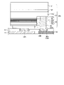
図17は、第6変形例に係る赤色発光素子を示す断面図である。表示装置1において、発光素子3はフェースアップ構造に限定されず、発光素子3の下部が、アノード電極23及びカソード電極22に接続される、いわゆるフェースダウン構造であってもよい。図17では、発光素子3のうち、赤色発光素子3Raの断面構造を示す。
図18は、第7変形例に係る赤色発光素子を示す断面図である。図18に示すように、第7変形例の赤色発光素子3Rbにおいて、発光層34の第1発光層34a及び第2発光層34bは、同層に設けられる。第1発光層34a及び第2発光層34bは、p型クラッド層35の上において、隣接して設けられる。第1発光層34aの上面及び第2発光層34bの上面は、n型クラッド層33に接し、第1発光層34aの下面及び第2発光層34bの下面は、p型クラッド層35に接する。
図19は、第8変形例に係る赤色発光素子を示す断面図である。図19に示すように、第8変形例の赤色発光素子3Rcにおいて、p型クラッド層35は、第3p型クラッド層35cを有する。第3p型クラッド層35cは、第1p型クラッド層35aとp型電極36との間に設けられる。第3p型クラッド層35cは、高濃度不純物領域が形成された窒化ガリウム(P+GaN)である。
図20は、第9変形例に係る赤色発光素子を示す断面図である。図20に示すように、第9変形例の赤色発光素子3Rdは、図7と同様に複数の部分発光素子3sを有している。赤色発光素子3Rdのp型クラッド層35は、第3p型クラッド層35cを有する。第3p型クラッド層35cは、高濃度不純物領域が形成された窒化ガリウム(P+GaN)である。第3p型クラッド層35cは、第1p型クラッド層35aとp型電極37との間に設けられる。また、発光層34は、第3p型クラッド層35c、第1p型クラッド層35a及び第2p型クラッド層35bと、n型クラッド層33との間に設けられる。
図21は、第10変形例に係る赤色発光素子を示す断面図である。図21に示すように、第10変形例の赤色発光素子3Reにおいて、発光層34の第1発光層34a及び第2発光層34bは、p型クラッド層35の上に,この順で積層されている。第1発光層34a及び第2発光層34bの積層の順番は逆であってもよい。
2 アレイ基板
3 発光素子
3R、3Ra、3Rb、3Rc、3Rd、3Re 赤色発光素子
3Ga 第1緑色発光素子
3Gb 第2緑色発光素子
3B 青色発光素子
12 駆動回路
21 基板
49R 第1画素
49Ga 第2画素
49Gb 第3画素
49B 第4画素
61、65、71、71A、75、79 半導体層
64、66、74、78 ゲート電極
62、72 ソース電極
67、73、77 ドレイン電極
61a 第1部分半導体層
210 駆動IC
100、100A 信号処理回路
110 第1処理回路
115 メモリ
120 第2処理回路
125 バッファ
DRT 駆動トランジスタ
BCT 出力トランジスタ
IST 初期化トランジスタ
SST 画素選択トランジスタ
RST リセットトランジスタ
PVDD アノード電源電位
PVSS カソード電源電位
L1 アノード電源線
L2 映像信号線
L3 リセット電源線
L4 初期化電源線
L5 リセット制御信号線
L6 出力制御信号線
L7 画素制御信号線
L8 初期化制御信号線
L9 接続配線
Claims (12)
- 基板と、
前記基板に設けられた複数の画素と、を有し、
複数の前記画素の各々は、赤色発光素子と第1緑色発光素子とを含み、
赤色を表示させる入力信号に基づいて前記第1緑色発光素子が前記赤色発光素子と同時に点灯する時、前記第1緑色発光素子の発光強度は、前記赤色発光素子の発光強度よりも小さく、かつ、前記第1緑色発光素子の光のスペクトルの半値幅は、前記赤色発光素子の光のスペクトルの半値幅よりも大きい
表示装置。 - 複数の前記画素の各々は、さらに、第2緑色発光素子を有し、
前記第2緑色発光素子の発光強度は、前記第1緑色発光素子の発光強度よりも大きい
請求項1に記載の表示装置。 - 前記第1緑色発光素子の光のスペクトルの極大発光波長は、前記第2緑色発光素子の光のスペクトルの極大発光波長よりも長く、前記赤色発光素子の光のスペクトルの極大発光波長よりも短い
請求項2に記載の表示装置。 - 複数の前記画素の各々は、さらに、青色発光素子を有し、
前記赤色発光素子と前記第1緑色発光素子とは、第1方向に並び、
前記赤色発光素子と、前記第2緑色発光素子又は前記青色発光素子の一方とは、前記第1方向と交差する第2方向に並ぶ
請求項2に記載の表示装置。 - 複数の前記画素の各々は、さらに、青色発光素子を有し、
前記赤色発光素子と、前記第2緑色発光素子又は前記青色発光素子の一方とは、第1方向に並び、
前記赤色発光素子と、前記第2緑色発光素子又は前記青色発光素子の他方とは、前記第1方向と交差する第2方向に並ぶ
請求項2に記載の表示装置。 - 前記画素の入力階調値が第1しきい値以下の場合に前記赤色発光素子が点灯し、前記第1緑色発光素子が点灯せず、
前記画素の入力階調値が前記第1しきい値よりも大きく、且つ、前記第1しきい値よりも大きい第2しきい値よりも小さい場合に前記赤色発光素子及び前記第1緑色発光素子が点灯する
請求項1に記載の表示装置。 - 前記画素の入力階調値が前記第2しきい値以上の場合に前記赤色発光素子が点灯し、前記第1緑色発光素子が点灯しない、
請求項6に記載の表示装置。 - 複数の前記画素の各々は、第1画素と、前記第1画素に隣接する第2画素を含み、
前記第1画素の入力階調値に基づいて、前記第1画素の前記第1緑色発光素子の第1階調値と、前記第2画素の前記第1緑色発光素子の第2階調値とを演算し、前記第1画素の前記第1緑色発光素子と前記第2画素の前記第1緑色発光素子とが点灯され、
前記第1画素の前記入力階調値に基づいて点灯される前記第1画素の前記第1緑色発光素子に供給される駆動電流がしきい値電流よりも大きい場合に、前記第1画素の前記第1緑色発光素子が前記第1階調値より低い第1出力階調値で点灯し、前記第2画素の前記第1緑色発光素子が前記第2階調値より高い第2出力階調値で点灯する、
請求項1に記載の表示装置。 - 前記第2出力階調値は、前記第2階調値と第3階調値との和であり、
前記第3階調値は、前記第1階調値と前記第1出力階調値との差である、
請求項8に記載の表示装置。 - 前記赤色発光素子の発光層は、ユウロピウム(Eu)が添加された窒化ガリウム(GaN)を含む
請求項1に記載の表示装置。 - 赤色を表示させる第1入力信号に基づいて発光する第1赤色発光素子及び第1緑色発光素子を含む第1画素と、
前記第1画素に隣接し、赤色を表示させる第2入力信号に基づいて発光する第2赤色発光素子及び第2緑色発光素子を含む第2画素と、
信号処理回路と
を有し、
前記第1入力信号は、赤色の入力階調値を含み、
前記第2緑色発光素子は、前記第1入力信号に基づいて発光することが可能であり、
前記第1入力信号に基づいて前記第2緑色発光素子が発光する時、
前記信号処理回路は、前記入力階調値に基づいて、前記第1緑色発光素子の第1階調値と、前記第2緑色発光素子の第2階調値とを出力し、
前記第1緑色発光素子に供給される、前記第1階調値に基づく駆動電流が、しきい値電流よりも大きい時、
前記第1階調値より低い第3階調値で、前記第1緑色発光素子が点灯し、
前記第2階調値より高い第4階調値で、前記第2緑色発光素子が点灯する、表示装置。 - 前記第4階調値は、前記第2階調値と第5階調値との和であり、
前記第5階調値は、前記第1階調値と前記第3階調値との差である、
請求項11に記載の表示装置。
Priority Applications (4)
| Application Number | Priority Date | Filing Date | Title |
|---|---|---|---|
| JP2018207672A JP7149164B2 (ja) | 2018-11-02 | 2018-11-02 | 表示装置 |
| PCT/JP2019/031662 WO2020090185A1 (ja) | 2018-11-02 | 2019-08-09 | 表示装置 |
| TW108136230A TWI803702B (zh) | 2018-11-02 | 2019-10-07 | 顯示裝置 |
| US17/244,477 US11362078B2 (en) | 2018-11-02 | 2021-04-29 | Display device |
Applications Claiming Priority (1)
| Application Number | Priority Date | Filing Date | Title |
|---|---|---|---|
| JP2018207672A JP7149164B2 (ja) | 2018-11-02 | 2018-11-02 | 表示装置 |
Publications (3)
| Publication Number | Publication Date |
|---|---|
| JP2020071456A JP2020071456A (ja) | 2020-05-07 |
| JP2020071456A5 JP2020071456A5 (ja) | 2021-12-16 |
| JP7149164B2 true JP7149164B2 (ja) | 2022-10-06 |
Family
ID=70464419
Family Applications (1)
| Application Number | Title | Priority Date | Filing Date |
|---|---|---|---|
| JP2018207672A Active JP7149164B2 (ja) | 2018-11-02 | 2018-11-02 | 表示装置 |
Country Status (4)
| Country | Link |
|---|---|
| US (1) | US11362078B2 (ja) |
| JP (1) | JP7149164B2 (ja) |
| TW (1) | TWI803702B (ja) |
| WO (1) | WO2020090185A1 (ja) |
Families Citing this family (2)
| Publication number | Priority date | Publication date | Assignee | Title |
|---|---|---|---|---|
| US11309351B2 (en) * | 2019-02-20 | 2022-04-19 | Sharp Kabushiki Kaisha | Micro light-emitting diode and manufacturing method of micro light-emitting diode |
| TWI800271B (zh) * | 2021-11-09 | 2023-04-21 | 友達光電股份有限公司 | 顯示裝置及其漏電流偵測方法 |
Citations (8)
| Publication number | Priority date | Publication date | Assignee | Title |
|---|---|---|---|---|
| JP2003315778A (ja) | 2002-04-25 | 2003-11-06 | Toppan Printing Co Ltd | 液晶表示装置 |
| WO2004072931A1 (en) | 2003-02-13 | 2004-08-26 | Seam Tech Corporation | Multi-scanning control process and led displaying device |
| US20100327263A1 (en) | 2009-06-24 | 2010-12-30 | Au Optronics Corporation | OLED panel with broadended color spectral components |
| US20130175514A1 (en) | 2012-01-09 | 2013-07-11 | Samsung Display Co., Ltd. | Display device |
| US20160155376A1 (en) | 2014-11-28 | 2016-06-02 | Samsung Display Co., Ltd. | Method of performing a multi-time programmable (mtp) operation and organic light-emitting diode (oled) display employing the same |
| WO2016152321A1 (ja) | 2015-03-20 | 2016-09-29 | ソニーセミコンダクタソリューションズ株式会社 | 表示装置および照明装置ならびに発光素子および半導体デバイス |
| US20170191786A1 (en) | 2015-04-21 | 2017-07-06 | Michael Hunter | Torque reducing apparatus and method |
| JP2018040875A (ja) | 2016-09-06 | 2018-03-15 | 株式会社半導体エネルギー研究所 | ハイブリッド表示装置、およびその駆動方法 |
Family Cites Families (27)
| Publication number | Priority date | Publication date | Assignee | Title |
|---|---|---|---|---|
| JP3124208B2 (ja) * | 1995-03-30 | 2001-01-15 | 株式会社東芝 | Led表示器及びled表示システム |
| US20020125821A1 (en) * | 2001-03-12 | 2002-09-12 | University Of Cincinnati | Electroluminescent display formed on glass with a thick film dielectric layer |
| JP2005062833A (ja) * | 2003-07-29 | 2005-03-10 | Seiko Epson Corp | カラーフィルタ、カラー画像表示装置および電子機器 |
| JPWO2006001254A1 (ja) * | 2004-06-29 | 2008-04-17 | 株式会社ニコン | イメージコンバイナ及び画像表示装置 |
| KR101252089B1 (ko) * | 2006-06-30 | 2013-04-12 | 엘지디스플레이 주식회사 | 액정 표시 장치 |
| US7830428B2 (en) * | 2007-04-12 | 2010-11-09 | Aptina Imaging Corporation | Method, apparatus and system providing green-green imbalance compensation |
| WO2009072428A1 (ja) * | 2007-12-05 | 2009-06-11 | Sony Corporation | 表示装置 |
| TW200931363A (en) * | 2008-01-10 | 2009-07-16 | Ind Tech Res Inst | Flat display panel |
| US8409897B2 (en) | 2009-05-07 | 2013-04-02 | Osaka University | Production method of red light emitting semiconductor device |
| JP2011023999A (ja) * | 2009-07-16 | 2011-02-03 | Fuji Xerox Co Ltd | 画像読み取り装置 |
| JP6274771B2 (ja) * | 2013-07-26 | 2018-02-07 | 株式会社ジャパンディスプレイ | 発光素子表示装置 |
| JP2015041633A (ja) * | 2013-08-20 | 2015-03-02 | 船井電機株式会社 | 食品用照明装置および精肉用照明装置 |
| JP5878579B2 (ja) * | 2014-03-31 | 2016-03-08 | シャープ株式会社 | 表示装置及びテレビ受信装置 |
| WO2016038508A1 (en) * | 2014-09-12 | 2016-03-17 | Semiconductor Energy Laboratory Co., Ltd. | Display device |
| JP2016071334A (ja) * | 2014-09-26 | 2016-05-09 | 株式会社ジャパンディスプレイ | 表示装置 |
| US9900957B2 (en) * | 2015-06-11 | 2018-02-20 | Cree, Inc. | Lighting device including solid state emitters with adjustable control |
| US10380930B2 (en) * | 2015-08-24 | 2019-08-13 | X-Celeprint Limited | Heterogeneous light emitter display system |
| WO2017191786A1 (ja) * | 2016-05-02 | 2017-11-09 | シャープ株式会社 | 表示装置およびその製造方法 |
| CN109565916B (zh) * | 2016-07-28 | 2021-02-05 | 夏普株式会社 | 显示装置的制造方法和显示装置 |
| JP6884537B2 (ja) * | 2016-09-20 | 2021-06-09 | 株式会社半導体エネルギー研究所 | 表示装置 |
| US10177195B2 (en) | 2016-09-30 | 2019-01-08 | Intel Corporation | Micro-LED displays |
| US20190221719A1 (en) * | 2018-01-17 | 2019-07-18 | Huizhou China Star Optoelectronics Technology Co., Ltd. | Backlight source |
| CN108596124A (zh) * | 2018-04-28 | 2018-09-28 | 京东方科技集团股份有限公司 | 指纹识别面板、指纹识别方法及显示装置 |
| CN111430556A (zh) * | 2018-06-29 | 2020-07-17 | 云谷(固安)科技有限公司 | 有机电致发光器件和有机电致发光装置 |
| US10854706B2 (en) * | 2018-09-11 | 2020-12-01 | Innolux Corporation | Tiled electronic system and tiled electronic unit |
| US20200173645A1 (en) * | 2018-11-30 | 2020-06-04 | Johnson Controls Technology Company | Multicolor led display of actuator function |
| WO2020121904A1 (ja) * | 2018-12-14 | 2020-06-18 | 国立大学法人大阪大学 | 表示装置およびその製造方法 |
-
2018
- 2018-11-02 JP JP2018207672A patent/JP7149164B2/ja active Active
-
2019
- 2019-08-09 WO PCT/JP2019/031662 patent/WO2020090185A1/ja active Application Filing
- 2019-10-07 TW TW108136230A patent/TWI803702B/zh active
-
2021
- 2021-04-29 US US17/244,477 patent/US11362078B2/en active Active
Patent Citations (8)
| Publication number | Priority date | Publication date | Assignee | Title |
|---|---|---|---|---|
| JP2003315778A (ja) | 2002-04-25 | 2003-11-06 | Toppan Printing Co Ltd | 液晶表示装置 |
| WO2004072931A1 (en) | 2003-02-13 | 2004-08-26 | Seam Tech Corporation | Multi-scanning control process and led displaying device |
| US20100327263A1 (en) | 2009-06-24 | 2010-12-30 | Au Optronics Corporation | OLED panel with broadended color spectral components |
| US20130175514A1 (en) | 2012-01-09 | 2013-07-11 | Samsung Display Co., Ltd. | Display device |
| US20160155376A1 (en) | 2014-11-28 | 2016-06-02 | Samsung Display Co., Ltd. | Method of performing a multi-time programmable (mtp) operation and organic light-emitting diode (oled) display employing the same |
| WO2016152321A1 (ja) | 2015-03-20 | 2016-09-29 | ソニーセミコンダクタソリューションズ株式会社 | 表示装置および照明装置ならびに発光素子および半導体デバイス |
| US20170191786A1 (en) | 2015-04-21 | 2017-07-06 | Michael Hunter | Torque reducing apparatus and method |
| JP2018040875A (ja) | 2016-09-06 | 2018-03-15 | 株式会社半導体エネルギー研究所 | ハイブリッド表示装置、およびその駆動方法 |
Also Published As
| Publication number | Publication date |
|---|---|
| JP2020071456A (ja) | 2020-05-07 |
| WO2020090185A1 (ja) | 2020-05-07 |
| TWI803702B (zh) | 2023-06-01 |
| US20210249394A1 (en) | 2021-08-12 |
| US11362078B2 (en) | 2022-06-14 |
| TW202107430A (zh) | 2021-02-16 |
Similar Documents
| Publication | Publication Date | Title |
|---|---|---|
| US10804317B2 (en) | Stretchable display apparatus | |
| TWI808248B (zh) | 顯示裝置 | |
| TWI738058B (zh) | 顯示裝置及陣列基板 | |
| US7994522B2 (en) | Organic light emitting element and organic light emitting device | |
| US11824150B2 (en) | Display device and array substrate | |
| US11764254B2 (en) | Display apparatus | |
| US20210210474A1 (en) | Display device and array substrate | |
| US11362078B2 (en) | Display device | |
| WO2022168431A1 (ja) | 表示装置 | |
| US20220037303A1 (en) | Display device | |
| US20210082893A1 (en) | Display device and array substrate | |
| US20230155030A1 (en) | Array substrate and display device including thereof | |
| US20240063250A1 (en) | Display device and method for manufacturing the same | |
| US20220399320A1 (en) | Display device | |
| US20240105902A1 (en) | Display device |
Legal Events
| Date | Code | Title | Description |
|---|---|---|---|
| A521 | Request for written amendment filed |
Free format text: JAPANESE INTERMEDIATE CODE: A523 Effective date: 20211101 |
|
| A621 | Written request for application examination |
Free format text: JAPANESE INTERMEDIATE CODE: A621 Effective date: 20211101 |
|
| A131 | Notification of reasons for refusal |
Free format text: JAPANESE INTERMEDIATE CODE: A131 Effective date: 20220705 |
|
| A521 | Request for written amendment filed |
Free format text: JAPANESE INTERMEDIATE CODE: A523 Effective date: 20220822 |
|
| TRDD | Decision of grant or rejection written | ||
| A01 | Written decision to grant a patent or to grant a registration (utility model) |
Free format text: JAPANESE INTERMEDIATE CODE: A01 Effective date: 20220906 |
|
| A61 | First payment of annual fees (during grant procedure) |
Free format text: JAPANESE INTERMEDIATE CODE: A61 Effective date: 20220926 |
|
| R150 | Certificate of patent or registration of utility model |
Ref document number: 7149164 Country of ref document: JP Free format text: JAPANESE INTERMEDIATE CODE: R150 |