JP7127042B2 - 光電変換モジュール及び光電変換モジュールを製造する方法 - Google Patents
光電変換モジュール及び光電変換モジュールを製造する方法 Download PDFInfo
- Publication number
- JP7127042B2 JP7127042B2 JP2019542010A JP2019542010A JP7127042B2 JP 7127042 B2 JP7127042 B2 JP 7127042B2 JP 2019542010 A JP2019542010 A JP 2019542010A JP 2019542010 A JP2019542010 A JP 2019542010A JP 7127042 B2 JP7127042 B2 JP 7127042B2
- Authority
- JP
- Japan
- Prior art keywords
- photoelectric conversion
- electrode layer
- region
- grid
- conversion module
- Prior art date
- Legal status (The legal status is an assumption and is not a legal conclusion. Google has not performed a legal analysis and makes no representation as to the accuracy of the status listed.)
- Active
Links
Images


Classifications
-
- H—ELECTRICITY
- H10—SEMICONDUCTOR DEVICES; ELECTRIC SOLID-STATE DEVICES NOT OTHERWISE PROVIDED FOR
- H10F—INORGANIC SEMICONDUCTOR DEVICES SENSITIVE TO INFRARED RADIATION, LIGHT, ELECTROMAGNETIC RADIATION OF SHORTER WAVELENGTH OR CORPUSCULAR RADIATION
- H10F19/00—Integrated devices, or assemblies of multiple devices, comprising at least one photovoltaic cell covered by group H10F10/00, e.g. photovoltaic modules
- H10F19/30—Integrated devices, or assemblies of multiple devices, comprising at least one photovoltaic cell covered by group H10F10/00, e.g. photovoltaic modules comprising thin-film photovoltaic cells
- H10F19/31—Integrated devices, or assemblies of multiple devices, comprising at least one photovoltaic cell covered by group H10F10/00, e.g. photovoltaic modules comprising thin-film photovoltaic cells having multiple laterally adjacent thin-film photovoltaic cells deposited on the same substrate
- H10F19/35—Structures for the connecting of adjacent photovoltaic cells, e.g. interconnections or insulating spacers
-
- H—ELECTRICITY
- H10—SEMICONDUCTOR DEVICES; ELECTRIC SOLID-STATE DEVICES NOT OTHERWISE PROVIDED FOR
- H10F—INORGANIC SEMICONDUCTOR DEVICES SENSITIVE TO INFRARED RADIATION, LIGHT, ELECTROMAGNETIC RADIATION OF SHORTER WAVELENGTH OR CORPUSCULAR RADIATION
- H10F71/00—Manufacture or treatment of devices covered by this subclass
- H10F71/138—Manufacture of transparent electrodes, e.g. transparent conductive oxides [TCO] or indium tin oxide [ITO] electrodes
-
- H—ELECTRICITY
- H10—SEMICONDUCTOR DEVICES; ELECTRIC SOLID-STATE DEVICES NOT OTHERWISE PROVIDED FOR
- H10F—INORGANIC SEMICONDUCTOR DEVICES SENSITIVE TO INFRARED RADIATION, LIGHT, ELECTROMAGNETIC RADIATION OF SHORTER WAVELENGTH OR CORPUSCULAR RADIATION
- H10F77/00—Constructional details of devices covered by this subclass
- H10F77/20—Electrodes
- H10F77/206—Electrodes for devices having potential barriers
- H10F77/211—Electrodes for devices having potential barriers for photovoltaic cells
- H10F77/215—Geometries of grid contacts
-
- H—ELECTRICITY
- H10—SEMICONDUCTOR DEVICES; ELECTRIC SOLID-STATE DEVICES NOT OTHERWISE PROVIDED FOR
- H10F—INORGANIC SEMICONDUCTOR DEVICES SENSITIVE TO INFRARED RADIATION, LIGHT, ELECTROMAGNETIC RADIATION OF SHORTER WAVELENGTH OR CORPUSCULAR RADIATION
- H10F77/00—Constructional details of devices covered by this subclass
- H10F77/20—Electrodes
- H10F77/244—Electrodes made of transparent conductive layers, e.g. transparent conductive oxide [TCO] layers
Landscapes
- Photovoltaic Devices (AREA)
Description
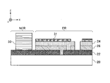
図1は、第1実施形態に係る光電変換モジュールの模式的上面図である。図2は、図1の領域2Rにおける光電変換モジュールの模式的上面図である。図3は、図2の3A-3A線に沿った光電変換モジュールの模式的断面図である。図4は、図2の領域4Rにおける光電変換モジュールの模式的斜視図である。図5は、図1の5A-5A線に沿った光電変換モジュールの模式的断面図である。図6は、図1の領域6Rにおける光電変換モジュールの模式的上面図である。図7は、図1の領域7Rにおける光電変換モジュールの模式的上面図である。
12 光電変換セル
20 基板
22 第1電極層
24 第2電極層(n型半導体)
26 光電変換層(p型半導体)
31 第1グリッド電極
32 第2グリッド電極
50 配線
Claims (5)
- 第1電極層と、第2電極層と、前記第1電極層と前記第2電極層との間の光電変換層と、を含む光電変換セルと、
前記光電変換セルにおいて第1方向に並んで設けられ、前記第1方向に交差する方向に延びる複数のグリッド電極と、を有し、
前記第1電極層と前記第2電極層の少なくとも一方は透明電極層であり、
前記透明電極層は、第1領域及び第2領域を含み、
前記第2領域は、前記第1領域におけるシート抵抗よりも小さいシート抵抗、前記第1領域における膜厚よりも大きい膜厚、又は前記第1領域における透過率よりも小さい透過率を有し、
前記第1領域において前記第1方向に互いに隣り合う前記グリッド電極どうしの間隔は、前記第2領域において前記第1方向に互いに隣り合う前記グリッド電極どうしの間隔よりも小さい、光電変換モジュール。 - 前記第1領域と前記第2領域は、同一の前記光電変換セル内に配置される、請求項1に記載の光電変換モジュール。
- 前記第1領域と前記第2領域は、互いに異なる前記光電変換セルに配置される、請求項1に記載の光電変換モジュール。
- 前記透明電極層は、シート抵抗、膜厚又は透過率に分布を有し、
前記第1方向に互いに隣り合う前記グリッド電極のどうしの間隔は、前記シート抵抗が大きいほど小さく、前記膜厚が小さいほど小さく、又は前記透過率が大きいほど小さい、請求項1から3のいずれか1項に記載の光電変換モジュール。 - 基板上に、第1電極層と、第2電極層と、前記第1電極層と前記第2電極層との間の光電変換層と、を含む帯状の光電変換セルを形成するセル形成工程であって、前記第1電極層と前記第2電極層の少なくとも一方は透明電極層であるセル形成工程と、
前記透明電極層のシート抵抗、膜厚又は透過率を測定する工程と、
前記光電変換セルにおいて第1方向に並んで設けられ、前記第1方向に交差する方向に延びる複数のグリッド電極を形成するグリッド形成工程と、を有し、
前記グリッド形成工程では、大きいシート抵抗を有する領域、小さい膜厚を有する領域、又は大きい透過率を有する領域ほどグリッド電極のどうしの間隔が小さくなるように、グリッド電極が形成される、光電変換モジュールを製造する方法。
Applications Claiming Priority (3)
| Application Number | Priority Date | Filing Date | Title |
|---|---|---|---|
| JP2017178367 | 2017-09-15 | ||
| JP2017178367 | 2017-09-15 | ||
| PCT/JP2018/032774 WO2019054239A1 (ja) | 2017-09-15 | 2018-09-04 | 光電変換モジュール及び光電変換モジュールを製造する方法 |
Publications (2)
| Publication Number | Publication Date |
|---|---|
| JPWO2019054239A1 JPWO2019054239A1 (ja) | 2020-10-22 |
| JP7127042B2 true JP7127042B2 (ja) | 2022-08-29 |
Family
ID=65722794
Family Applications (1)
| Application Number | Title | Priority Date | Filing Date |
|---|---|---|---|
| JP2019542010A Active JP7127042B2 (ja) | 2017-09-15 | 2018-09-04 | 光電変換モジュール及び光電変換モジュールを製造する方法 |
Country Status (4)
| Country | Link |
|---|---|
| US (1) | US20210028322A1 (ja) |
| JP (1) | JP7127042B2 (ja) |
| CN (1) | CN111247643B (ja) |
| WO (1) | WO2019054239A1 (ja) |
Families Citing this family (4)
| Publication number | Priority date | Publication date | Assignee | Title |
|---|---|---|---|---|
| DE102021127720A1 (de) * | 2021-10-25 | 2023-04-27 | Heliatek Gmbh | Elektrisch leitfähige Beschichtung eines elektrischen Bauelements zur elektrisch leitfähigen Kontaktierung einer außerhalb der Beschichtung angeordneten Sammelschiene |
| EP4470038A4 (en) * | 2022-01-27 | 2025-03-26 | Triumph Science & Technology Group Co., Ltd | INKJET PRINTER FOR FORMING CROSSED CONDUCTIVE LINES OF THIN FILM SOLAR MODULE AND AUTOMATED METALLIZATION SYSTEM |
| CN115763628A (zh) * | 2022-11-25 | 2023-03-07 | 凯盛光伏材料有限公司 | 一种cigs薄膜太阳能电池组件及其制备方法 |
| CN115775844A (zh) * | 2022-11-25 | 2023-03-10 | 凯盛光伏材料有限公司 | 一种cigs薄膜太阳能电池导电栅线的制备及刻线设备 |
Citations (6)
| Publication number | Priority date | Publication date | Assignee | Title |
|---|---|---|---|---|
| JP2000058888A (ja) | 1998-08-03 | 2000-02-25 | Sanyo Electric Co Ltd | 太陽電池及びその製造方法 |
| WO2009142187A1 (ja) | 2008-05-22 | 2009-11-26 | 株式会社カネカ | 薄膜光電変換装置とその製造方法 |
| JP2012124328A (ja) | 2010-12-08 | 2012-06-28 | Ulvac Japan Ltd | 太陽電池 |
| WO2013094233A1 (ja) | 2011-12-21 | 2013-06-27 | 三菱電機株式会社 | 太陽電池およびその製造方法、太陽電池モジュール |
| US20160284882A1 (en) | 2013-09-17 | 2016-09-29 | Lg Innotek Co., Ltd. | Solar Cell |
| JP2017126750A (ja) | 2016-01-14 | 2017-07-20 | エルジー エレクトロニクス インコーポレイティド | 太陽電池 |
Family Cites Families (10)
| Publication number | Priority date | Publication date | Assignee | Title |
|---|---|---|---|---|
| US4590327A (en) * | 1984-09-24 | 1986-05-20 | Energy Conversion Devices, Inc. | Photovoltaic device and method |
| JPS63143878A (ja) * | 1986-12-08 | 1988-06-16 | Matsushita Electric Ind Co Ltd | シリコン太陽電池 |
| JPH03234066A (ja) * | 1990-02-09 | 1991-10-18 | Sanyo Electric Co Ltd | 光起電力装置 |
| CN1093985C (zh) * | 1996-05-17 | 2002-11-06 | 佳能株式会社 | 光电元件的制造方法 |
| JP2008277233A (ja) * | 2007-04-03 | 2008-11-13 | Oike Ind Co Ltd | 透明導電性フィルム及びその製造方法 |
| JP2011216189A (ja) * | 2010-03-31 | 2011-10-27 | Sony Corp | 光電変換装置及び光電変換装置モジュール |
| JP5829101B2 (ja) * | 2011-10-28 | 2015-12-09 | オリンパス株式会社 | 神経刺激装置および埋込型心臓治療装置 |
| JP2013219143A (ja) * | 2012-04-06 | 2013-10-24 | Sharp Corp | 薄膜太陽電池モジュールおよび薄膜太陽電池モジュールの製造方法 |
| JP2015195341A (ja) * | 2014-03-24 | 2015-11-05 | 三菱電機株式会社 | 光電変換素子および光電変換素子の製造方法 |
| JP6422426B2 (ja) * | 2014-12-09 | 2018-11-14 | 三菱電機株式会社 | 太陽電池 |
-
2018
- 2018-09-04 JP JP2019542010A patent/JP7127042B2/ja active Active
- 2018-09-04 CN CN201880059780.3A patent/CN111247643B/zh active Active
- 2018-09-04 WO PCT/JP2018/032774 patent/WO2019054239A1/ja not_active Ceased
- 2018-09-04 US US16/647,160 patent/US20210028322A1/en not_active Abandoned
Patent Citations (6)
| Publication number | Priority date | Publication date | Assignee | Title |
|---|---|---|---|---|
| JP2000058888A (ja) | 1998-08-03 | 2000-02-25 | Sanyo Electric Co Ltd | 太陽電池及びその製造方法 |
| WO2009142187A1 (ja) | 2008-05-22 | 2009-11-26 | 株式会社カネカ | 薄膜光電変換装置とその製造方法 |
| JP2012124328A (ja) | 2010-12-08 | 2012-06-28 | Ulvac Japan Ltd | 太陽電池 |
| WO2013094233A1 (ja) | 2011-12-21 | 2013-06-27 | 三菱電機株式会社 | 太陽電池およびその製造方法、太陽電池モジュール |
| US20160284882A1 (en) | 2013-09-17 | 2016-09-29 | Lg Innotek Co., Ltd. | Solar Cell |
| JP2017126750A (ja) | 2016-01-14 | 2017-07-20 | エルジー エレクトロニクス インコーポレイティド | 太陽電池 |
Also Published As
| Publication number | Publication date |
|---|---|
| WO2019054239A1 (ja) | 2019-03-21 |
| CN111247643A (zh) | 2020-06-05 |
| US20210028322A1 (en) | 2021-01-28 |
| CN111247643B (zh) | 2023-09-22 |
| JPWO2019054239A1 (ja) | 2020-10-22 |
Similar Documents
| Publication | Publication Date | Title |
|---|---|---|
| KR101283053B1 (ko) | 태양광 발전장치 및 이의 제조방법 | |
| JP7127042B2 (ja) | 光電変換モジュール及び光電変換モジュールを製造する方法 | |
| US20150040962A1 (en) | Solar Cell and Method of Fabricating the Same | |
| CN102272938B (zh) | 光电转换元件、光电转换模块及光电转换元件的制造方法 | |
| CN102132419A (zh) | 光电转换元件及光电转换模块 | |
| KR101241467B1 (ko) | 태양전지 및 이의 제조방법 | |
| KR101283072B1 (ko) | 태양광 발전장치 및 이의 제조방법 | |
| KR101428146B1 (ko) | 태양전지 모듈 및 이의 제조방법 | |
| KR101189309B1 (ko) | 태양전지 및 태양전지 모듈 | |
| KR20120073767A (ko) | 박막태양전지 및 그 제조방법 | |
| KR101114169B1 (ko) | 태양광 발전장치 | |
| KR101550927B1 (ko) | 태양전지 및 이의 제조방법 | |
| JP7053202B2 (ja) | 光電変換モジュール | |
| CN111247642B (zh) | 光电变换模块以及制造光电变换模块的方法 | |
| KR101338610B1 (ko) | 태양광 발전장치 및 이의 제조방법 | |
| KR101272997B1 (ko) | 태양광 발전장치 및 이의 제조방법 | |
| KR101173418B1 (ko) | 태양전지 및 이의 제조방법 | |
| JP6185840B2 (ja) | 太陽光発電装置及びその製造方法 | |
| JP2019054166A (ja) | 光電変換モジュールの製造方法 | |
| KR101306525B1 (ko) | 태양전지 모듈 및 이의 제조방법 | |
| JP2013149699A (ja) | 集積化太陽電池の製造方法 | |
| KR101543034B1 (ko) | 팁 및 이를 이용한 태양전지의 제조방법 | |
| JP2011091224A (ja) | 集積型光発電素子及び集積型光発電素子の製造方法 | |
| KR20140047258A (ko) | 태양전지 및 이의 제조 방법 | |
| KR101306436B1 (ko) | 태양광 발전장치 및 이의 제조방법 |
Legal Events
| Date | Code | Title | Description |
|---|---|---|---|
| A521 | Request for written amendment filed |
Free format text: JAPANESE INTERMEDIATE CODE: A523 Effective date: 20200131 |
|
| A621 | Written request for application examination |
Free format text: JAPANESE INTERMEDIATE CODE: A621 Effective date: 20210831 |
|
| TRDD | Decision of grant or rejection written | ||
| A01 | Written decision to grant a patent or to grant a registration (utility model) |
Free format text: JAPANESE INTERMEDIATE CODE: A01 Effective date: 20220719 |
|
| A61 | First payment of annual fees (during grant procedure) |
Free format text: JAPANESE INTERMEDIATE CODE: A61 Effective date: 20220817 |
|
| R150 | Certificate of patent or registration of utility model |
Ref document number: 7127042 Country of ref document: JP Free format text: JAPANESE INTERMEDIATE CODE: R150 |